EP2529484B1 - Arrangement and system for an inductive sensor push-button - Google Patents
Arrangement and system for an inductive sensor push-button Download PDFInfo
- Publication number
- EP2529484B1 EP2529484B1 EP20110703823 EP11703823A EP2529484B1 EP 2529484 B1 EP2529484 B1 EP 2529484B1 EP 20110703823 EP20110703823 EP 20110703823 EP 11703823 A EP11703823 A EP 11703823A EP 2529484 B1 EP2529484 B1 EP 2529484B1
- Authority
- EP
- European Patent Office
- Prior art keywords
- section
- sensor coil
- frame
- target
- circuit board
- Prior art date
- Legal status (The legal status is an assumption and is not a legal conclusion. Google has not performed a legal analysis and makes no representation as to the accuracy of the status listed.)
- Not-in-force
Links
Images


Classifications
-
- H—ELECTRICITY
- H03—ELECTRONIC CIRCUITRY
- H03K—PULSE TECHNIQUE
- H03K17/00—Electronic switching or gating, i.e. not by contact-making and –breaking
- H03K17/94—Electronic switching or gating, i.e. not by contact-making and –breaking characterised by the way in which the control signals are generated
- H03K17/96—Touch switches
-
- H—ELECTRICITY
- H03—ELECTRONIC CIRCUITRY
- H03K—PULSE TECHNIQUE
- H03K17/00—Electronic switching or gating, i.e. not by contact-making and –breaking
- H03K17/94—Electronic switching or gating, i.e. not by contact-making and –breaking characterised by the way in which the control signals are generated
- H03K17/965—Switches controlled by moving an element forming part of the switch
- H03K17/97—Switches controlled by moving an element forming part of the switch using a magnetic movable element
- H03K2017/9706—Inductive element
-
- H—ELECTRICITY
- H03—ELECTRONIC CIRCUITRY
- H03K—PULSE TECHNIQUE
- H03K2217/00—Indexing scheme related to electronic switching or gating, i.e. not by contact-making or -breaking covered by H03K17/00
- H03K2217/94—Indexing scheme related to electronic switching or gating, i.e. not by contact-making or -breaking covered by H03K17/00 characterised by the way in which the control signal is generated
- H03K2217/96—Touch switches
- H03K2217/96038—Inductive touch switches
Definitions
- the invention relates to an arrangement for an inductive key switch and a system hereby according to claims 1 and 12.
- inductive sensor switches and their circuits are known.
- MICROCHIP TECHNOLOGY INC. MICROCHIP
- Chandler, Ariz. Published an arrangement design 10 for inductive proximity switches (the "MICROCHIP design") which provides a magnetic coupling between a solid metal target 12 and an inductive measuring or sensing coil 14 separated by a spacer layer 16 are used.
- the spacer layer 16 defines a cavity or pocket into which the solid metal target 12 may flex when pressed, thereby printing and / or attaching its proximity to the sensor coil 14 attached to a PCB PCB 19 etched in such, and change the surrounding field.
- the front panel 18 also referred to as the top key switch layer or cover, may be the outermost skin of the product or home appliance, of which the keyboard is a part.
- the MICROCHIP design assumes that copper, aluminum, measurement, stainless steel, and mild steel are materials of choice for a cover layer / target combination, however, a target in accordance with the design could also be made of gold and / or silver as long as the material allows for physical deformation of the target over the sensor coil.
- Specific target embodiments disclosed in the MICROCHIP design include a copper cladding and one on the underside of the Cover set self adhesive or adhesive copper label.
- the MICROCHIP design states that, in general, the target 12 should have the size and shape of the sensor coil 14.
- a microcontroller is provided to periodically interrogate various sensors by measuring the impedance of a sensing coil. If the impedance of the sensing coil has changed, the microcontroller determines whether the change in impedance is sufficient to classify it as user pressure.
- the individual sensing coils ie, one for each switch
- the reference choke coil serving as the reference choke coil, allowing a ratio metric measurement that eliminates multiple drift sources.
- the inductive sensing circuit of the MICROCHIP design uses a single driver circuit to drive each of the sensing coils, each of which is connected by a common connection to the reference coil.
- the outer material of a key switch (the cover) is made of a relatively thick, for example, 0.032 to 0.036 inch thick piece of stainless steel.
- the cover is made of a relatively thick, for example, 0.032 to 0.036 inch thick piece of stainless steel.
- a 2.15 diameter measuring coil Customs require. Such a measuring coil diameter would be impractical for the landscape format of the device keyboard, ie would require a key spacing of more than 2 inches. It has also been found that with such materials, a drive current can be so high had to be that eddy currents are generated in the metal.
- the MICROCHIP design assumes that, as an alternative solution, the reference coil can be eliminated and provided to compensate for the drift software.
- the MICROCHIP design specifically discloses that such software can become bulky and the burden on the microcontroller may increase significantly, whereas the inclusion of the reference choke on the card is minimal, which is why the MICROCHIP design specifically states that omitting the reference coil is not recommended as soon as the increase in software size is considered.
- pressure-sensitive inductive switches are known from the US 2009/0160789 A1 and the DE 20 2008 001 970 U1 known.
- the present invention is therefore based on the problem, an arrangement and a system for a to provide inductive sensor switch that eliminates the disadvantages of the prior art.
- an arrangement for an inductive sensor switch comprising: a user interface front panel section; a sensor coil disposed on a circuit board; a conductive target disposed between the user interface panel section and the sensor coil; a frame disposed between the circuit board and the user interface front panel section, the frame including a bridging section having an uppermost surface adjacent the lower surface of the user interface front panel section and a lowermost surface facing the sensor coil , wherein the conductive target is located proximal to the lowermost surface of the bridging portion, whereby deflection of the faceplate portion above the frame results in deflection of the bridging portion and movement of at least a portion of the conductive target toward the sensor coil.
- a system for an inductive sensor key switch comprising: a plurality of inductive sensor key switch assemblies each of said inductive sensor key switch assemblies comprising a conductive target coupled to a sensor coil; a plurality of drive circuits that generate a drive current, each of the plurality of drive circuits comprising their own drive transistor, and wherein each of the plurality of drive circuits provides drive current to only one of the plurality of inductive sensor load switch arrangements.
- a system has several arrangements for an inductive sensor key switch, wherein each sensor coil is connected directly to ground via a common supply line connection.
- the assembly further comprises at least one light emitter disposed on the circuit board, and wherein at least a portion of the frame is made of a translucent material, wherein the translucent portion of the frame is in optical communication with an emitting portion of the at least one light emitter is arranged.
- the target is attached directly to the lowermost surface of a bridging section.
- the conductive target is fixed by hot stamping and / or printing to the lowermost surface of the bridging section.
- the frame further comprises a bead portion projecting from the bridging portion, the conductive target being disposed away from the bridging portion in communication with the bead portion.
- the conductive target is attached to the distal bead portion and floats over the sensor coil.
- the conductive target is a metal disc.
- the conductive target is a sheet of a multi-leaf target.
- the conductive target is a conductive cap which is mounted between the circuit board and the bead portion and above the sensor coil on the circuit board.
- the conductive cap is either a dome-shaped or a box-shaped or a footed disc.
- the sensor coil comprises a first set of windings which rotate in a first direction and a second set of windings which rotate in a second direction, the second direction being opposite to the first direction, the second set of windings surrounds the first set of turns.
- the sensor coil comprises a first set of turns, the arrangement further comprising at least one additional turn disposed outside the first set of turns, the at least one additional turn being shorted to a reference potential.
- At least one sensor coil is a multi-level sensor coil.
- the inductive sensor load switch arrangement comprises: a user interface front panel section; a sensor coil disposed on a first circuit board; a conductive target disposed between the user interface front panel section and the sensor coil; a second circuit board disposed between the first circuit board having the sensor coil and the user interface front panel section; a frame disposed between the second circuit board and the user interface front panel section, the frame including a bridging section having an uppermost surface adjacent to a lower surface of the user interface front panel section and a lowermost surface facing the uppermost surface of the user interface PCB, wherein the frame further comprises a bead portion which is from the bottom surface of the bridging portion, wherein the distal portion of the bead portion to a portion of the uppermost surface of the second printed circuit board adjacent to or is arranged in connection therewith the conductive target is disposed on a portion of a lower surface of the second circuit board below the bead portion such that flexing of the user interface front panel portion above the frame results in deflection of the a
- each of the plurality of drive circuits is disposed on the circuit board local to that arrangement for the inductive sensor key switch to which it provides a drive current.
- At least one of the plurality of sensor inductive sensing switch assemblies includes a faceplate portion, the conductive target being adjacent but spaced apart from the sensor coil of the at least one inductive proximity sensing switch assembly, the sensor coil being disposed on a printed circuit board.
- a second printed circuit board is arranged between the printed circuit board with the sensor coil and the front panel section and a frame between the second printed circuit board and the front panel section.
- the frame comprises a bridging portion having an uppermost surface adjacent to a lower surface of the faceplate portion and a lowermost surface facing the second printed circuit board.
- the frame comprises a bead portion that projects from the bottom surface of the bridging portion, wherein the distal portion of the bead portion is adjacent to or communicating with a portion of a front surface of the second printed circuit board.
- the conductive target is disposed at a portion of a back surface of the second circuit board below the bead portion so that deflection of the panel portion above the frame results in deflection of the panel Bridging portion results whose force is transferable through the bead portion on the second circuit board, whereby the second circuit board is bendable and the coupling of the conductive target is changeable with the sensor coil.
- each inductive sensor key assembly includes a translucent key element supported by a frame, the target being disposed on a rearward outer surface of the translucent key element.
- an improved inductive sensor switch is provided.
- a circuit for inductive sensing switches that eliminates the reference inductor without requiring the addition of extensive software.
- the present invention relates to an inductive sensor key switch and its associated control circuit, the inductive sensor key user interface being suitable for use with a control circuit having driver elements spatially associated with the respective key switch.
- an arrangement and circuit for inductive sensor switches are provided which, under certain circumstances, can be used to control both signal strength and signal strength Noise immunity of the present invention over those of the MICROCHIP design.
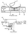
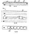
- Fig. 2 a block diagram of a system 20 for inductive sensor key switch of the prior art in accordance with the teachings of the MICROCHIP design shown.
- the system 20 To measure the impedance of a respective sensor or measuring coil 26, the system 20 generates a pulse at the pulse width modulator (PWM) 22 which is converted by the driver 24 into a drive pulse which is used to energize a respective sensor coil 26 again.
- PWM pulse width modulator
- the pulse voltage from the sensor coil 26 is further processed and analyzed to determine if there has been a change in impedance indicating contact by the user.
- PWM pulse width modulator
- the sensor coils 26 are each connected at one end to a reference coil 28 via a single common connection.
- the connection with such a reference coil forces the creation of long PCB design paths which, especially with long keyboards, pick up the noise and reduce the signal strength.
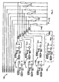
- a particular embodiment of a circuit 100 for inductive sensor keyswitches of the present invention is shown which provides for improved noise immunity and enhanced signal strength transmission.
- the number of long, noisy paths inherent in the prior art system is greatly reduced.
- each of the sensor coils 110 of the system 100 is connected to the common connection directly (ie not via any other series connected circuit element) to ground 112 and not to a reference coil, eliminating the need to route each sensor coil one path to a common one Pull reference coil.
- no energy goes to the reference coil, causing the ratio change when a key press is detected is reduced.
- software filtering to compensate for the drift is added instead of the omitted reference coil.
- the circuit 100 also eliminates long paths from a common driver circuit to each sensor coil 110 by providing individual drive or driver circuits 120 for energizing the respective coils 110.
- each of the driver circuits 120 is provided locally (ie, in close proximity) to the sensor coil 110 that drives it.
- the driver circuit 120a is disposed near the sensor coil 110a on the PCB.
- the remainder of the individual driver circuits 120 are located on the printed circuit board (PCB) near its associated sensor coil 110, which is driven by the single driver circuit 120.
- PCB printed circuit board
- the metal forming the sensor coil 162 is placed next to the metal traces 166 and contacts or pads 164 for the driver circuit elements (ie, a driver transistor, one or more input resistors, one or more output resistors, etc.) on the PCB.
- the driver circuit elements ie, a driver transistor, one or more input resistors, one or more output resistors, etc.
- the metallization for the contacts for the driver coil associated with that sensor coil 162 is located at most a few millimeters from the outermost turn of the sensor coil 162, thus shortening the lead lengths between a drive circuit and the sensor coil 162 driving it can.
- each of the plurality of drive circuits 120 includes its own driver transistor T1 and resistor and capacitor elements used to define the drive current.
- each of the driver circuits 120 comprises at least one driver transistor T1, a first input resistor connected between the base of the transistor T1 and a clock input for the respective driver circuit 120 Rin1, a second input resistor Rin2 connected between the base of T1 and a DC power supply, an output resistance Rout, and a capacitor C1.
- Rin1 is 470 ohms
- Rin2 is 100 ohms
- Rout is 270 ohms
- C1 is 1 ⁇ F
- the power supply is 5 volts DC.
- inductors 110 is selected based on a number of factors including the outside radius of the coil, the number of turns in the coil, and the depth of the coil. Each sensor coil 110 is connected via an in Figure 3 Scanned output shown periodically scanned by a microcontroller or microprocessor (not shown). It should be noted that although the transistor T1 is shown as a pnp transistor, this is not to be construed restrictively, since the circuit can be adapted to the use of an npn transistor.
- each sensor coil 110 of this embodiment is driven by only one driver circuit 120, and conversely, each driver circuit 120 drives only one associated sensor coil 110.
- Locally locating each of a plurality of drive circuits to their associated one of the sensor coils results in a small circuit through the sensor coil of each key array without greatly radiating current / noise from the coil to the outside. The less current / noise emitted by the coil to the outside, the less it can be absorbed by other sensor coils.
- the noise pickup by the coil can be further reduced by taking a short turn outside of the PCB film Coil is added. This may slightly reduce the signal strength; however, since it is outside the coil surface and the coil-induced field is concentrated near the coil pattern, it does not cause much signal strength reduction. However, the shortened turn reduces uniform external fields as they come from outside the coil pattern.
- the noise pick-up by the sensor coil can be further reduced by adding turns outside the sensor coil as an extension of the sensor coil, but in the opposite direction. See for example Figure 17 where the turns 510 of the sensor coil 500 rotate in a first direction, but the other way around the turn section 515 to have multiple turns 520 in the opposite direction.
- the use of such additional turns 520 reduces the field strength such that, relative to external fields, the loop surface of the sensor coil minus the loop surface of the turns leads in the opposite direction to a take-up by (N coil-x reverse turns) 2 . It should be noted that only a few large opposing turns equal the loop area of many small turns in the coil.
- Fig. 18 is now another embodiment of a multi-level or multi-layer sensor coil 530 used as a sensor coil in a system in FIG Agreement can be used with the present invention shown.
- the multilayer sensor coil 530 includes two individual sensor coils 540, 550 overlapping each other on the surface of the PCB (not shown) and sharing the commonly connected input and output contacts 542, 552 and 544, 554.
- the coil 550 is wound in a direction opposite to that of the coil 540 and covers the coil 540 on the PCB.
- Both input contacts 542 are connected to a measuring input (for example in FIG Fig. 3 shown) of a microcontroller or microprocessor (not shown) programmed to evaluate the measurements made on the sensor coil 530.
- the output contacts 544 and 554 are connected to a common reference potential, such as ground.
- the multilayer coil provides greater field strength and better eddy currents that result in better signal return when target movement occurs.
- the PCB may further include staggered vias to avoid blind vias and help keep costs low. It should be noted that although in the explanatory illustration of FIG Fig. 18 two coils are shown, this is not to be construed restrictive, since more coil layers can be provided as needed. Note, however, increasing the number of coil layers in the sensor coil 530 decreases the distance between the uppermost surface of the sensor coil 530 and the target portion of the key switch, due to the increased thickness of the layers on the PCB. In order to accommodate the increased layer height at the PCB, an appropriate adjustment to the distance between the uppermost coil layer and the target can be made as needed.
- the driver circuits 120 can be configured as needed to allow for driver-to-key variations in driver strength. For example, differently sized keys (and their associated coils) may have different signal strength levels need.
- the drive voltage can be changed from one sensor coil / sensor key coordination to the other by a fixed value. Alternatively, as needed, the drive voltage may be changed from one sensor to another as a software variable using an adaptive algorithm.
- Another advantage of associating the driver 120 with the location of the associated sensor coil 110 is that the delay of the drive pulse can be optimized to bring all useful signals into the detector as compared to a synchronous detector system.
- the delay can be greatly improved by offsetting the driver transistor and the sense resistor to the coil location since previous drive pulse delay times were affected by temperature variation and part deviation.
- coils may be stacked in double-sided PCBs.
- four coil layers were stacked by offsetting the via to avoid hidden vias.
- a sensor inductive load switch assembly 200 that provides improved signal strength and mechanical stability in a sensor inductive load switch system in accordance with a particular embodiment of the present invention.
- the key switch assembly 200 of this embodiment is located under a portion of the front panel or cover 218 (ie, the keyboard, product, and / or home appliance front panel) that defines a user interface push-button.
- the front panel 218 and thus the user interface is one thin stainless steel plate.
- the prior art push-button assembly illustrated in FIG. 2 does not staple the target 212 of the key switch assembly 200 to the underside of the cover 218, but instead supports it with a frame 216 disposed between the cover 218 and the PCB 219.
- the frame 216 is formed as a bracket or pocket defining a space or cavity 217 about the sensor coil 214.
- the frame 216 is a separate, separate piece made of plastic and includes a support bracket 216 surrounding the sensor coil 214, at the top of which is a bridging portion 216a located at a location defining a push-button on the user interface of the front panel 218.
- a support bracket 216 surrounding the sensor coil 214, at the top of which is a bridging portion 216a located at a location defining a push-button on the user interface of the front panel 218.
- a bridging portion 216a located at a location defining a push-button on the user interface of the front panel 218.
- the support bracket 216 may be made as a frame (i.e., four feet or four walls, etc.) or in the form of a ring covered by the bridging portion 216a. This frame may be connected to the PCB 216 by screws, hot-inserted connectors, or other conventional connection methods.
- the bridging portion 216a is designed of very thin plastic so that the deflection of the cover 218 results in a deflection of the bridging portion 216a.
- the thickness "A" of the bridging portion 216a is 0.8 mm.
- the metal target 212 on the underside of the bridging portion is also deflected, thereby changing between the target 212 and the sensor coil 214, indicating depression of the key switch.
- the target 212 is supported by a structure that exists between the Front panel cover 218 and the PCB 219 is arranged, and not directly attached to the underside of the front panel cover 218.
- the target 212 of the key switch assembly 200 is instead attached to the underside of the bridging portion 216a to bring the target 212 into the desired relationship with the sensor coil 214.
- the target 212 is attached to the underside of the bridging section as part of a hot stamping process.
- the target 212 may be attached to the underside of the bridging portion 216a by printing the target directly on the back of the cover to provide a metal surface over the sensor coil.
- a hot stamped film or conductive print material may be applied to the frame 216 by any suitable process (i.e., hot stamping, printing, etc.). Hot stamping or printing of the target 212 onto a surface of the frame 216 rather than the cover 218 may be particularly useful in applications where adjacent lighting is needed and / or curved surfaces are used.
- a portion of the front panel 218 defines a user interface or keyboard for a product or home appliance.
- a metal foil is embossed on the inner surface of the plastic bracket or bag.
- the film desirably has a thickness between 0.05 mm and 0.1 mm.
- the conventional PCB-based keypads are replaced by a hot-stamped foil or printed conductive layer supported by a separate yoke.
- a printing process may be used to apply a conductive material to the underside of the substrate Bridging section 216a to print.
- the thickness of the printed material would be similar to that for the hot embossed film, ie most preferably between 0.05 mm and 0.1 mm.
- a key switch assembly 220 in accordance with the present invention is shown.
- the key switch assembly 220 is similar to the key switch assembly 200 of FIG Figure 4 however, it is directed to a user interface having push buttons with any type of illuminated sign such as words, light rings, and / or other light indicators, but having an opaque plate.
- the key switch assembly 220 includes a target 212 attached to the bridging portion 226a of a frame 226 in a particular plane with respect to a sensor coil 214.
- the deflection of the key switch cover 228 results in the deflection of the bridge portion 226a which alters the coupling between the target 212 and the sensor coil 214, thus indicating a key depression of the key switch cover 228.
- the frame 226 of this embodiment is made of clear or other translucent plastic so that light emitted by a light source can be transmitted to the ring, words, or characters on the user interface.
- a light source ie, incandescent lamp, electroluminescent source, etc.
- the light source includes light emitting diodes (LEDs) 230 mounted on the underside of the PCB 229.
- the plastic frame comprises a translucent ring portion 226b surrounding an opaque key switch cover 228.
- the key switch cover 228 may itself have stamped portions such as words or other indicia intended to be illuminated.
- Light emitted by the LEDs 230 is used to label the ring and / or the characters follows to illuminate.
- the light from the LEDs 230 passes through the PCB 229 through holes 222 in the PCB 229 that are adjacent to the light emitting side of the LEDs.
- the holes 222 open into the cavity 227 formed in the frame between the target 212 and the sensor coil 214.
- the frame 226 may optionally include facets 226c, particularly arranged to direct and concentrate light emitted by the LEDs 230 into the cavity 227 on the light ring portions 226b.
- the frame 226 may include opaque or opaque portions 224 as needed to prevent the light emitted in conjunction with a key switch assembly from being transferred to another key switch assembly.
- a white coating is applied to the PCB 226 disposed in the cavity 227 to further reflect light from the cavity 227 into the translucent frame 226.
- the target 212 of the key switch assembly 220 may be variously including, but not limited to, hot stamping the target 212 onto the frame 226 and / or printing the target 212 onto the frame 226 using a conductive ink at Frame 226 may be attached. It should be noted that, if desired, the target 212 may also be formed as a metal disc or foil adhered to the underside of the bridging portion 226a without departing from the spirit of the present invention.
- the key switch assembly 300 includes a frame 310 disposed between the PCB 302 and the front panel 318 of the user interface of a device, which is in communication with Fig. 4 frame 216 is similar.
- the frame 310 of the assembly 300 includes a bridging portion 310a that is adjacent to and in contact with the underside of the front panel 318 at a location defining a key switch on the front panel 318.
- the bridging portion is preferably made of a thin plastic material having a thickness "B" that allows it to deflect in response to the deflection of the face plate 318. In a particular embodiment, the dimension "B" is 0.8 mm.
- the frame 310 also includes a push pin or bead 310b that extends from the center of the bridging portion 310a toward the sensor coil 320.
- the target 330 communicates with the distal end of the bead 310b and has a circumference larger than the circumference of the sensor coil 320 so as to circumscribe the sensor coil 320.
- deflection of the front panel 318 over the bridging portion 310a causes the pusher pin 310b to push a portion of the target 330, thus deflecting the target 330 and altering the coupling between the target 330 and the sensor coil 320, indicating depression of the key switch .
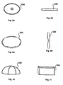
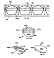
- the target 330 as a hood-shaped cap, which in Fig. 10 is shown more clearly formed.
- a footed "disk" 332 which instead of the target 330 of Fig. 6 on the PCB 302 may be surface mounted (via the extending foot portions), wherein the deflection of the face plate 318 above the frame 310 causes the bead 310b to deflect the feet washer 332 and thus the coupling between the target 332 and the sensor coil 320 changed, indicating that one Push-button is pressed.
- the footed disc 332 from the Figs. 9A and 9B may be formed by chemical etching and / or embossing of the metal to be used as a target.
- a target 334 having the shape of a square or rectangle may be placed over the sensor coil 320 and deflected by the front panel 318 above the frame 310 Bead 310b are activated.
- a sensor load switch assembly 340 which uses a frame 350 having a bead 350a to transmit the deflection of the key switch cover 228 to the target 330 mounted on the PCB, using light from a light source, the LEDs 230 in this embodiment, passes through holes 222 in the PCB 355.
- the frame 350 is made of a translucent material such as a clear plastic. The frame 350 is therefore aligned with the holes 222 to cause light to project from the ring portions 350b as well as any words or characters punched into the key switch cover 228.
- LEDs 230 and the holes 222 may be arranged such that in the same manner as in connection with the frame 226 of FIG Fig. 5 has been described, the central cavity 317 of the frame 350 and thereby the frame 350 and the ring portions 350b are illuminated.
- FIGS. 12 and 13 There are now two further illuminated key switch assemblies 400 and 430, respectively, in accordance with further embodiments of the present invention Invention shown. Exactly shows Fig. 12 a key switch assembly 400 in which LEDs 410 are mounted on the front of the PCB 415, with their light-emitting outer surfaces facing the sidewalls of the frame 420. In Fig. 13 For example, the LEDs 450 on the PCB 445 are surface mounted in the cavity 447 of the frame 440 with their light emitting outer surfaces facing the front panel 457. From the foregoing, it will be understood that other configurations of a lighting key switch assembly may be implemented by means of a translucent frame in conjunction with a target in accordance with the present invention.
- FIG. 14 Now another embodiment of a key switch assembly 500 in accordance with the present invention is shown.
- the key switch assembly 500 is similar in many ways to the key switch assembly 300 of FIG Fig. 6 , However, instead of using a surface mounted target sandwiched between the bead and the PCB, as in the key switch assembly 200, this embodiment uses a floating target 510 attached to the bead 310b. Thus, deflection of the bridging portion 310a, rather than causing the target 510 to deflect, causes the target closer to the sensor coil 214, whereby its field is changed and a key press is displayed.
- the target 510 is a cut-out or punched-out disk, such as those shown in FIGS Figs. 8A and 8B
- the diameter of the disc 338, 510 may be selected as needed, but is preferably equal to or greater than the diameter of the sensor coil 320.
- the floating target 510 of FIG Fig. 14 can be used in a light key arrangement.
- the floating target 510 may include the surface mounted target 330 in the key switch assembly 340 of FIG Fig. 7 or in any other embodiment described herein.
- FIG. 15 Now, another embodiment of a sensor inductive switch 550 arrangement in accordance with the present invention is shown.
- the frame 560 instead of being disposed between and in communication with the PCB 555 and the front panel 318, the frame 560 is sandwiched between a ground plane PCB 565 and the front panel 318 that overlies the PCB 555 that supports the sensor coil 320 arranged.
- the ground plane PCB 565 is separated from the PCB 555 by a spacer 570 having a circular cut-out over the sensor coil 320, creating a cavity or chamber over the sensor coil 320.
- the frame 560 is supported by its outer wall portions over solid portions of the spacer layer on the ground plane PCB 565, whereby the frame 560 is supported when a push button switch indicated on the face plate 318 above the assembly 550 is pressed.
- the frame also has a bead 560a extending from its central portion, which is in contact with a portion of the ground plane PCB 565. Deflection of the front panel 318 above the bead 560a causes the bead 560a to deflect the PCB 565.
- the portion of the PCB 565 disposed below the bead 560a includes a metal target 570 located at the bottom thereof adjacent the sensor coil 320.
- the deflection of the front panel 318 is transmitted through the frame 560 to the target 570, which facilitates coupling between the target 570 and the sensor coil 320 changes, indicating that a pushbutton located above the user interface assembly has been pressed.
- the target 570 is either printed on or hot stamped onto the lower surface of the PCB 565. It should be noted that other methods of applying the target 570 to the PCB 565 including all methods of creating a metallization of a PCB.
- the keyboard 600 includes a plurality of illuminated key switches 640, where the key switch elements 640 serve as both optical fibers for transmitting the light through the cover or faceplate 610 and as a force translator for moving the target with respect to the sensor coil.
- a backlit pushbutton 640 is provided having light bulges 640a forming a light ring and passing through apertures 610a in the opaque faceplate 610.
- the key switch elements 640 are held in place in a frame 620 disposed between the front panel 610 and a PCB 630.
- the frame 620 may be secured by the adhesive layers 615 disposed between the frame 620 and the PCB 630 and the frame 620 and the face plate 610. As in the previous embodiments, each key switch is disposed over a corresponding sensor coil disposed on the PCB 630 in the frame. The frame 620 may be aligned as needed by the alignment pins 622 with respect to the front panel 610.
- Each key switch element 640 is designed to mate with an opening 620a of the frame 620 with the light transmitting protrusions 640 passing through the front panel 610 of the assembly 600.
- a flat outer surface 640c of the key switch element 640 is provided to support an adhesive layer and / or the front panel 610.
- the key switch member 640 is held in the frame by the tabs 640b and the groove 640e, which engage the rear of the frame 620, that is, the side remote from the front outer surface 610 (as in FIG Fig. 20B is shown).
- a target in the Fig. 19 - 21 not shown
- the target is a piece of metal foil bonded to the rear outer surface 640d.
- each key switch element 640 is supported over a sensor coil by the frame 620 and / or an adhesive layer 612 (which does not pass under the portion of the key switch element 640 that includes the target).
- the target on the rearward outer surface 640d of each key switch element 640 is disposed in the desired relationship with a sensor coil, as has been described elsewhere herein.
- the inductive keying circuit of the present invention may be modified to include a reference coil implemented at a key position of the keyboard.
- the reference coil is used to provide drift compensation as a standard reference, with no key movement is allowed to assist.
Abstract
Description
Die Erfindung betrifft eine Anordnung für einen induktiven Tastschalter sowie ein System hiermit gemäß den Ansprüchen 1 und 12.The invention relates to an arrangement for an inductive key switch and a system hereby according to
Im Grunde sind induktive Sensortastschalter und deren Schaltungen bekannt. Um auf
Es besteht ein Bedarf an einem verbesserten Targetentwurf zur Verwendung mit einem System für induktiven Sensortastschalter.There is a need for an improved target design for use with a sensor inductive sensor system.
Außerdem ist in Übereinstimmung mit dem MICROCHIP-Entwurf ein Mikrocontroller vorgesehen, um verschiedene Sensoren periodisch abzufragen, indem die Impedanz einer Messspule gemessen wird. Wenn sich die Impedanz der Messspule verändert hat, ermittelt der Mikrocontroller, ob die Veränderung der Impedanz hinreichend ist, um dies als Drücken durch einen Benutzer einzustufen. Beim MICROCHIP-Entwurf sind die einzelnen Messspulen (d. h. eine für jeden Schalter) durch eine einzige gemeinsame Verbindung mit einer "Referenzspule", die als Referenzdrosselspule dient, verbunden, was eine verhältnismetrische Messung ermöglicht, die mehrere Driftquellen beseitigt. Wie in
Jedoch ist bei vielen Anwendungen das äußere Material eines Tastschalters (der Abdeckung) aus einem relativ dicken, beispielsweise 0,032 bis 0,036 Zoll dicken, Stück Edelstahl gefertigt. Jedoch würde das Verwenden der beim MICROCHIP-Entwurf gelehrten Berechnungen zum Erzeugen einer 0,010 mm-Bewegung eines induktiven Tastschalters mit einer Targetabdeckungs-/Targetdicke von 0,036 Zoll bei einem Tastendrücken mit einer Kraft von 1,1 Pfund eine Messspule mit einem Durchmesser von 2,15 Zoll erfordern. Ein solcher Messspulendurchmesser wäre für das Querformat der Vorrichtungstastatur unpraktisch, d. h. würde einen Tastenabstand von mehr als 2 Zoll erfordern. Auch wurde festgestellt, dass bei solchen Materialien ein Treiberstrom so hoch sein musste, dass Wirbelströme im Metall erzeugt werden. Jedoch können höhere Treiberströme in den großen Treiberschleifen auf der PCB ein Nebensprechen und einen Verlust an Signalstärke verursachen. Außerdem können die Schaltungsschleifen Signale von externen Feldern aufnehmen (d. h., dass große Schleifen auf der PCB-Auslegung Rauschsignale aufnehmen können). Jedoch erzwingt die Verwendung von "Referenzspulen" im MICROCHIP-Entwurf die Einbeziehung großer Stromschleifen in der PCB-Auslegung, da jede Messspule in der Tastatur ihren Strom zur Referenzspule leiten muss. Diese Probleme eines stärkeren Rauschens und einer geringeren Signalstärke verschlimmern sich noch, wenn eine Tastatur eher lang als von kleiner, quadratischer Form ist.However, in many applications, the outer material of a key switch (the cover) is made of a relatively thick, for example, 0.032 to 0.036 inch thick piece of stainless steel. However, using the calculations taught in the MICROCHIP design to generate a 0.010 mm movement of a 0.036 inch target cap / target thickness inductive key switch with a 1.1 pound keystroke would require a 2.15 diameter measuring coil Customs require. Such a measuring coil diameter would be impractical for the landscape format of the device keyboard, ie would require a key spacing of more than 2 inches. It has also been found that with such materials, a drive current can be so high had to be that eddy currents are generated in the metal. However, higher drive currents in the large driver loops on the PCB can cause crosstalk and loss of signal strength. In addition, the circuit loops can pick up signals from external fields (ie, large loops on the PCB layout can pick up noise signals). However, the use of "reference coils" in the MICROCHIP design forces the inclusion of large current loops in the PCB design, as each sensing coil in the keyboard must direct its current to the reference coil. These problems of increased noise and signal strength are exacerbated when a keyboard is rather long rather than small, square in shape.
Der MICROCHIP-Entwurf geht davon aus, dass als eine alternative Lösung die Referenzspule entfallen kann und zur Kompensation der Drift Software bereitgestellt sein kann. Jedoch offenbart der MICROCHIP-Entwurf speziell, dass eine solche Software umfangreich werden kann und die Bürde für den Mikrocontroller wesentlich zunehmen kann, wohingegen die Einbeziehung der Referenzdrosselspule auf der Karte minimal ist, weshalb der MICROCHIP-Entwurf speziell anführt, dass das Weglassen der Referenzspule nicht empfohlen wird, sobald die Zunahme des Softwareumfangs in Betracht gezogen wird.The MICROCHIP design assumes that, as an alternative solution, the reference coil can be eliminated and provided to compensate for the drift software. However, the MICROCHIP design specifically discloses that such software can become bulky and the burden on the microcontroller may increase significantly, whereas the inclusion of the reference choke on the card is minimal, which is why the MICROCHIP design specifically states that omitting the reference coil is not recommended as soon as the increase in software size is considered.
Andere Beispiele für druckempfindliche induktive Schalter sind aus der
Benötigt wird ein induktiver Sensortastschalter mit Schaltung, der die Rauschunempfindlichkeit und die Signalstärke verbessert, ohne die in Verbindung mit dem MICROCHIP-Entwurf beschriebenen Hinzufügung der umfangreichen Software zu erfordern.What is needed is a circuit-type inductive sensor switch that improves noise immunity and signal strength without requiring the addition of the extensive software described in connection with the MICROCHIP design.
In Erkenntnis dieser Gegebenheiten liegt vorliegender Erfindung deshalb die Problemstellung zugrunde, eine Anordnung und ein System für einen induktiven Sensortastschalter zu schaffen, die bzw. das die Nachteile des Standes der Technik beseitigt.In recognition of these circumstances, the present invention is therefore based on the problem, an arrangement and a system for a to provide inductive sensor switch that eliminates the disadvantages of the prior art.
Die erstgenannte Aufgabe hinsichtlich einer Anordnung wird erfindungsgemäß gelöst durch eine Anordnung für einen induktiven Sensortastschalter, die umfasst: einen Benutzerschnittstelle-Frontplattenabschnitt; eine Sensorspule, die auf einer Leiterplatte angeordnet ist; ein leitendes Target, das zwischen dem Benutzerschnittstelte-Frontplattenabschnitt und der Sensorspule angeordnet ist; einen Rahmen, der zwischen der Leiterplatte und dem Benutzerschnittstelle-Frontplattenabschnitt angeordnet ist, wobei der Rahmen einen Überbrückungsabschnitt umfasst, das bzw. der eine oberste Oberfläche, die zur unteren Oberfläche des Benutzerschnittstelle-Frontplattenabschnitts benachbart ist, und eine unterste Oberfläche, die der Sensorspule zugewandt ist, besitzt, und wobei das leitende Target nächstgelegen zur untersten Oberfläche des Überbrückungsabschnitts angeordnet ist, wodurch eine Durchbiegung des Frontplattenabschnitts über dem Rahmen zu einer Durchbiegung des Überbrückungsabschnitts und einer Bewegung wenigstens eines Abschnitts des leitenden Targets zur Sensorspule hin führt.The first object with regard to an arrangement is achieved according to the invention by an arrangement for an inductive sensor switch, comprising: a user interface front panel section; a sensor coil disposed on a circuit board; a conductive target disposed between the user interface panel section and the sensor coil; a frame disposed between the circuit board and the user interface front panel section, the frame including a bridging section having an uppermost surface adjacent the lower surface of the user interface front panel section and a lowermost surface facing the sensor coil , wherein the conductive target is located proximal to the lowermost surface of the bridging portion, whereby deflection of the faceplate portion above the frame results in deflection of the bridging portion and movement of at least a portion of the conductive target toward the sensor coil.
Die zweitgenannte Aufgabe hinsichtlich eines Systems wird erfindungsgemäß gelöst durch ein System für einen induktiven Sensortastschalter, das umfasst: mehrere Anordnungen für einen induktiven Sensortastschalter wobei jede der Anordnungen für den induktiven Sensortastschalter ein leitendes Target umfasst, das mit einer Sensorspule gekoppelt ist; mehrere Treiberschaltungen, die einen Treiberstrom erzeugen, wobei jede der mehreren Treiberschaltungen ihren eigenen Treibertransistor umfasst und wobei jede der mehreren Treiberschaltungen nur an eine der mehreren Anordnungen für induktiven Sensortastschalter einen Treiberstrom liefert.The second object of a system according to the invention is achieved by a system for an inductive sensor key switch comprising: a plurality of inductive sensor key switch assemblies each of said inductive sensor key switch assemblies comprising a conductive target coupled to a sensor coil; a plurality of drive circuits that generate a drive current, each of the plurality of drive circuits comprising their own drive transistor, and wherein each of the plurality of drive circuits provides drive current to only one of the plurality of inductive sensor load switch arrangements.
In einer vorteilhaften Weiterbildung weist ein System mehrere Anordnungen für einen induktiven Sensortastschalter auf, wobei jede Sensorspule über eine gemeinsame Zuleitungsverbindung direkt mit Erde verbunden ist.In an advantageous development, a system has several arrangements for an inductive sensor key switch, wherein each sensor coil is connected directly to ground via a common supply line connection.
In einer bevorzugten Alternative umfasst die Anordnung ferner wenigstens einen Lichtemitter, der auf der Leiterplatte angeordnet ist, und wobei wenigstens ein Abschnitt des Rahmens aus einem lichtdurchlässigen Material gefertigt ist, wobei der lichtdurchlässige Abschnitt des Rahmens in optischer Verbindung mit einem emittierenden Abschnitt des wenigstens einen Lichtemitters angeordnet ist.In a preferred alternative, the assembly further comprises at least one light emitter disposed on the circuit board, and wherein at least a portion of the frame is made of a translucent material, wherein the translucent portion of the frame is in optical communication with an emitting portion of the at least one light emitter is arranged.
In einer weiteren Ausführungsform ist das Target direkt an der untersten Oberfläche eines Überbrückungsabschnitts befestigt.In another embodiment, the target is attached directly to the lowermost surface of a bridging section.
Vorteilhafter Weise ist das leitende Target durch Heißprägen und/oder Drucken an der untersten Oberfläche des Überbrückungsabschnitts befestigt.Advantageously, the conductive target is fixed by hot stamping and / or printing to the lowermost surface of the bridging section.
Zweckmäßiger Weise umfasst der Rahmen ferner einen Wulstabschnitt, der vom Überbrückungsabschnitt herab steht, wobei das leitende Target fern vom Überbrückungsabschnitt mit dem Wulstabschnitt in Verbindung stehend angeordnet ist.Conveniently, the frame further comprises a bead portion projecting from the bridging portion, the conductive target being disposed away from the bridging portion in communication with the bead portion.
In einer weiteren Ausgestaltung ist das leitende Target am fernen Wulstabschnitt befestigt und schwebt über der Sensorspule.In another embodiment, the conductive target is attached to the distal bead portion and floats over the sensor coil.
In einer besonders vorteilhaften Weiterbildung ist das leitende Target eine Metallscheibe. In einer weiteren Ausgestaltung ist das leitende Target ein Blatt eines mehrblättrigen Targets.In a particularly advantageous development, the conductive target is a metal disc. In a further embodiment, the conductive target is a sheet of a multi-leaf target.
Vorteilhafter Weise ist das leitende Target eine leitende Kappe, die zwischen der Leiterplatte und dem Wulstabschnitt und über der Sensorspule an der Leiterplatte angebracht ist.Advantageously, the conductive target is a conductive cap which is mounted between the circuit board and the bead portion and above the sensor coil on the circuit board.
Zweckmäßiger Weise ist die leitende Kappe entweder eine haubenförmige oder eine kastenförmige oder eine mit Füßen versehene Scheibe.Conveniently, the conductive cap is either a dome-shaped or a box-shaped or a footed disc.
In einer vorteilhaften Weiterbildung umfasst die Sensorspule einen ersten Satz von Windungen, die in einer ersten Richtung drehen, und einen zweiten Satz von Windungen, die in einer zweiten Richtung drehen, wobei die zweite Richtung zur ersten Richtung entgegengesetzt ist, wobei der zweite Satz von Windungen den ersten Satz von Windungen umgibt.In an advantageous development, the sensor coil comprises a first set of windings which rotate in a first direction and a second set of windings which rotate in a second direction, the second direction being opposite to the first direction, the second set of windings surrounds the first set of turns.
In einer bevorzugten Alternative umfasst die Sensorspule einen ersten Satz von Windungen, wobei die Anordnung ferner wenigstens eine zusätzliche Windung umfasst, die außerhalb des ersten Satzes von Windungen angeordnet ist, wobei die wenigstens eine zusätzliche Windung zu einem Bezugspotential kurzgeschlossen ist.In a preferred alternative, the sensor coil comprises a first set of turns, the arrangement further comprising at least one additional turn disposed outside the first set of turns, the at least one additional turn being shorted to a reference potential.
In einer weiteren Ausführungsform ist wenigstens eine Sensorspule eine Mehrebenen-Sensorspule.In another embodiment, at least one sensor coil is a multi-level sensor coil.
In einer besonders bevorzugten Ausführung umfasst die Anordnung für einen induktiven Sensortastschalter: einen Benutzerschnittstelle-Frontplattenabschnit; eine Sensorspule, die auf einer ersten Leiterplatte angeordnet ist; ein leitendes Target, das zwischen dem Benutzerschnittstelle-Frontplattenabschnitt und der Sensorspule angeordnet ist; eine zweite Leiterplatte, die zwischen der ersten Leiterplatte mit der Sensorspule und dem Benutzerschnittstelle-Frontplattenabschnitt angeordnet ist; einen Rahmen, der zwischen der zweiten Leiterplatte und dem Benutzerschnittstelle-Frontplattenabschnitt angeordnet ist, wobei der Rahmen einen Überbrückungsabschnitt umfasst, der eine oberste Oberfläche, die zu einer unteren Oberfläche des Benutzerschnittstelle-Frontplattenabschnitts benachbart ist, und eine unterste Oberfläche, die der obersten Oberfläche der Leiterplatte zugewandt ist, besitzt, wobei der Rahmen ferner einen Wulstabschnitt umfasst, der von der untersten Oberfläche des Überbrückungsabschnitts herab steht, wobei der ferne Abschnitt des Wulstabschnitts zu einem Abschnitt der obersten Oberfläche der zweiten Leiterplatte benachbart oder mit diesem in Verbindung stehend angeordnet ist und wobei das leitende Target auf einem Abschnitt einer tieferen Oberfläche der zweiten Leiterplatte unter dem Wulstabschnitt angeordnet ist, so dass eine Durchbiegung des Benutzerschnittstelle-Frontplattenabschnitts über dem Rahmen zu einer Durchbiegung des Überbrückungsabschnitts führt, deren Kraft durch den Wulstabschnitt auf die zweite Leiterplatte übertragen wird, womit die zweite Leiterplatte durchgebogen wird und die Kopplung des leitenden Targets mit der Sensorspule verändert wird.In a particularly preferred embodiment, the inductive sensor load switch arrangement comprises: a user interface front panel section; a sensor coil disposed on a first circuit board; a conductive target disposed between the user interface front panel section and the sensor coil; a second circuit board disposed between the first circuit board having the sensor coil and the user interface front panel section; a frame disposed between the second circuit board and the user interface front panel section, the frame including a bridging section having an uppermost surface adjacent to a lower surface of the user interface front panel section and a lowermost surface facing the uppermost surface of the user interface PCB, wherein the frame further comprises a bead portion which is from the bottom surface of the bridging portion, wherein the distal portion of the bead portion to a portion of the uppermost surface of the second printed circuit board adjacent to or is arranged in connection therewith the conductive target is disposed on a portion of a lower surface of the second circuit board below the bead portion such that flexing of the user interface front panel portion above the frame results in deflection of the bridging portion ts whose force is transmitted through the bead portion on the second circuit board, whereby the second circuit board is bent and the coupling of the conductive target is changed with the sensor coil.
Vorteilhafter Weise ist jede der mehreren Treiberschaltungen lokal zu jener Anordnung für den induktiven Sensortastschalter, zu der sie einen Treiberstrom liefert, auf der Leiterplatte angeordnet.Advantageously, each of the plurality of drive circuits is disposed on the circuit board local to that arrangement for the inductive sensor key switch to which it provides a drive current.
Zweckmäßiger Weise umfasst wenigstens eine der mehreren Anordnung für einen induktiven Sensortastschalter einen Frontplattenabschnitt, wobei das leitende Target zur Sensorspule der wenigstens einen Anordnung für einen induktiven Sensortastschalter benachbart, jedoch von dieser beabstandet angeordnet ist, wobei die Sensorspule auf einer Leiterplatte angeordnet ist.Conveniently, at least one of the plurality of sensor inductive sensing switch assemblies includes a faceplate portion, the conductive target being adjacent but spaced apart from the sensor coil of the at least one inductive proximity sensing switch assembly, the sensor coil being disposed on a printed circuit board.
In einer weiteren Ausgestaltung ist eine zweite Leiterplatte zwischen der Leiterplatte mit der Sensorspule und dem Frontplattenabschnitt und ein Rahmen zwischen der zweiten Leiterplatte und dem Frontplattenabschnitt angeordnet.In a further embodiment, a second printed circuit board is arranged between the printed circuit board with the sensor coil and the front panel section and a frame between the second printed circuit board and the front panel section.
Vorteilhafter Weise umfasst der Rahmen einen Überbrückungsabschnitt, der eine oberste Oberfläche, die zu einer unteren Oberfläche des Frontplattenabschnitts benachbart ist, und eine unterste Oberfläche, die der zweiten Leiterplatte zugewandt ist, aufweist.Advantageously, the frame comprises a bridging portion having an uppermost surface adjacent to a lower surface of the faceplate portion and a lowermost surface facing the second printed circuit board.
In einer besonders vorteilhaften Weiterbildung umfasst der Rahmen einen Wulstabschnitt, der von der untersten Oberfläche des Überbrückungsabschnitts herab steht, wobei der ferne Abschnitt des Wulstabschnitts zu einem Abschnitt einer vorderen Oberfläche der zweiten Leiterplatte benachbart oder mit diesem in Verbindung stehend angeordnet ist.In a particularly advantageous development, the frame comprises a bead portion that projects from the bottom surface of the bridging portion, wherein the distal portion of the bead portion is adjacent to or communicating with a portion of a front surface of the second printed circuit board.
In einer bevorzugten Alternative ist das leitende Target an einem Abschnitt einer hinteren Oberfläche der zweiten Leiterplatte unter dem Wulstabschnitt angeordnet, so dass eine Durchbiegung des Frontplattenabschnitts über dem Rahmen zu einer Durchbiegung des Überbrückungsabschnitts führt, deren Kraft durch den Wulstabschnitt auf die zweite Leiterplatte übertragbar ist, womit die zweite Leiterplatte durchbiegbar ist und die Kopplung des leitenden Targets mit der Sensorspule veränderbar ist.In a preferred alternative, the conductive target is disposed at a portion of a back surface of the second circuit board below the bead portion so that deflection of the panel portion above the frame results in deflection of the panel Bridging portion results whose force is transferable through the bead portion on the second circuit board, whereby the second circuit board is bendable and the coupling of the conductive target is changeable with the sensor coil.
In einer weiteren Ausführungsform umfasst jede Anordnung für die induktive Sensortaste ein lichtdurchlässiges Tastenelement, das durch einen Rahmen unterstützt ist, wobei das Target auf einer rückwärtigen Außenfläche des lichtdurchlässigen Tastenelements angeordnet ist.In another embodiment, each inductive sensor key assembly includes a translucent key element supported by a frame, the target being disposed on a rearward outer surface of the translucent key element.
In einer besonderen Ausführungsform der Erfindung wird ein verbesserter induktiver Sensortastschalter geschaffen. In einer weiteren Ausführungsform der Erfindung wird eine Schaltung für induktiven Sensortastschalter geschaffen, die die Referenzdrosselspule erübrigt, ohne die Hinzufügung umfangreicher Software zu erfordern.In a particular embodiment of the invention, an improved inductive sensor switch is provided. In another embodiment of the invention, there is provided a circuit for inductive sensing switches that eliminates the reference inductor without requiring the addition of extensive software.
Die vorliegende Erfindung bezieht sich auf einen induktiven Sensortastschalter und seine zugeordnete Steuerschaltung, wobei die Benutzerschnittstelle für induktiven Sensortastschalter zur Verwendung mit einer Steuerschaltung geeignet ist, die Treiberelemente besitzt, die dem jeweiligen Tastenschalter örtlich zugeordnet sind.The present invention relates to an inductive sensor key switch and its associated control circuit, the inductive sensor key user interface being suitable for use with a control circuit having driver elements spatially associated with the respective key switch.
Obwohl die Erfindung hier als in einer Anordnung und einer Schaltung für induktiven Sensortastschalter konkretisiert veranschaulicht und beschrieben wird, soll sie dennoch nicht auf die gezeigten Details beschränkt sein, da daran ohne Abweichung vom Leitgedanken der Erfindung und im Umfang und Bereich von Entsprechungen der Ansprüche liegend verschiedene Modifikationen und konstruktive Veränderungen vorgenommen werden können.Although the invention is illustrated and described as being concretely embodied herein in an arrangement and circuit for inductive sensor switches, it is not to be limited to the details shown, as is consistent with it without departing from the spirit of the invention and within the scope and range of equivalents of the claims Modifications and constructive changes can be made.
Die Konstruktion der Erfindung wird jedoch zusammen mit ihren weiteren Aufgaben und Vorteilen aus der folgenden Beschreibung der spezifischen Ausführungsformen am Besten verstanden, wenn sie in Verbindung mit den begleitenden Zeichnungen gelesen wird.However, the construction of the invention, together with its further objects and advantages, will be best understood from the following description of the specific embodiments when read in conjunction with the accompanying drawings.
Mehrere Ausführungsbeispiele werden anhand der Zeichnung und anhand der nachstehenden Beschreibung näher erläutert. Es zeigen:
- Fig. 1
- eine Querschnittsansicht einer Anordnung für einen induktiven Tast- bzw. Berührungssensor in Übereinstimmung mit dem Stand der Technik,
- Fig. 2
- ein Blockschaltplan einer induktiven Tastschaltung in Übereinstimmung mit dem Stand der Technik,
- Fig. 3
- einen Schaltplan einer Schaltung für einen induktiven Sensortastschalter in Übereinstimmung mit einer besonderen Ausführungsform der vorliegenden Erfindung,
- Fig. 4
- eine Querschnittsansicht einer Anordnung für einen induktiven Sensortastschalter in Übereinstimmung mit einer besonderen Ausführungsform der vorliegenden Erfindung,
- Fig. 5-7
- Querschnittsansichten einer Anordnung für einen induktiven Sensortastschalter in Übereinstimmung mit anderen besonderen Ausführungsformen der vorliegenden Erfindung,
- Fig. 8A
- eine isometrische Ansicht einer Scheibe, die als Target verwendet wird, in Übereinstimmung mit einer besonderen Ausführungsform der vorliegenden Erfindung,
- Fig. 8B
- eine Seitenrissansicht der Scheibe von
Fig. 8A , - Fig. 9A
- eine isometrische Ansicht einer mit Füßen versehenen Scheibe, die als Target verwendet wird, in Übereinstimmung mit einer besonderen Ausführungsform der vorliegenden Erfindung,
- Fig.9B
- eine Seitenrissansicht der mit Füßen versehenen Scheibe von
Fig. 9A , - Fig. 10
- eine Ansicht eines hauben- oder kappenförmigen Targets in Übereinstimmung mit einer weiteren Ausführungsform der vorliegenden Erfindung,
- Fig. 11
- eine isometrische Ansicht eines rechtwinkligen Targets in Übereinstimmung mit einer weiteren Ausführungsform der vorliegenden Erfindung,
- Fig. 12-15
- Querschnittsansichten einer Anordnung für induktiven Sensortastschalter in Übereinstimmung mit weiteren Ausführungsformen der vorliegenden Erfindung,
- Fig. 16
- eine Draufsicht einer besonderen Ausführungsform eines mehrblättrigen Targets in Übereinstimmung mit einer weiteren Ausführungsform der vorliegenden Erfindung,
- Fig. 17
- eine Draufsicht der Metallablagerungsschicht einer Sensorspule in Übereinstimmung mit einer besonderen Ausführungsform der vorliegenden Erfindung,
- Fig. 18
- eine perspektivische, auseinander gezogene Ansicht der Metallablagerungsschichten einer Spule in mehreren Ebenen in Übereinstimmung mit einer besonderen Ausführungsform der Erfindung,
- Fig. 19A
- eine teilweise, abgeschnittene Seitenrissansicht einer induktiven Tast- bzw. Berührungstastatur in Übereinstimmung mit einer besonderen Ausführungsform der Erfindung;
- Fig. 19B
- eine teilweise, auseinander gezogene Ansicht eines Abschnitts der Tastatur von
Fig. 19A , - Fig. 20A
- eine von oben aufgenommene, perspektivische Ansicht einer besonderen Ausführungsform eines Rahmens zur Verwendung in der Tastatur von
Fig. 19A , - Fig. 20B
- eine vergrößerte, teilweise Draufsicht eines Rahmens, der Tastschalterelemente enthält, in Übereinstimmung mit einer besonderen Ausführungsform,
- Fig. 21A
- eine Draufsicht eines Tastschalterelements in Übereinstimmung mit einer besonderen Ausführungsform der Erfindung,
- Fig. 21B
- eine von oben aufgenommene, perspektivische Ansicht des Tastschalterelements von
Fig. 21A , - Fig. 21C
- eine von unten aufgenommene, perspektivische Ansicht Tastschalterelements aus den
Fig. 21A und 21 B und - Fig. 22
- eine Draufsicht einer möglichen PCB-Auslegung für jede Anordnung für induktiven Sensortastschalter in Übereinstimmung mit einer besonderen Ausführungsform der vorliegenden Erfindung.
- Fig. 1
- a cross-sectional view of an arrangement for an inductive touch sensor according to the prior art,
- Fig. 2
- a block diagram of an inductive keying circuit in accordance with the prior art,
- Fig. 3
- 5 is a circuit diagram of a circuit for an inductive sensor switch in accordance with a particular embodiment of the present invention,
- Fig. 4
- a cross-sectional view of an arrangement for an inductive sensor switch in accordance with a particular embodiment of the present invention,
- Fig. 5-7
- Cross-sectional views of an arrangement for an inductive sensor switch in accordance with other particular embodiments of the present invention,
- Fig. 8A
- an isometric view of a target used in accordance with a particular embodiment of the present invention;
- Fig. 8B
- a side elevational view of the disc of
Fig. 8A . - Fig. 9A
- an isometric view of a footed disc used as a target in FIG In accordance with a particular embodiment of the present invention,
- Figure 9B
- a side elevational view of the footed disc of
Fig. 9A . - Fig. 10
- a view of a hood or cap-shaped target in accordance with another embodiment of the present invention,
- Fig. 11
- an isometric view of a rectangular target in accordance with another embodiment of the present invention,
- Fig. 12-15
- Cross-sectional views of an arrangement for inductive sensor switch in accordance with further embodiments of the present invention,
- Fig. 16
- a top view of a particular embodiment of a multi-leaf target in accordance with another embodiment of the present invention,
- Fig. 17
- a top view of the metal deposition layer of a sensor coil in accordance with a particular embodiment of the present invention,
- Fig. 18
- 3 is a perspective, exploded view of the metal deposition layers of a multilevel coil in accordance with a particular embodiment of the invention;
- Fig. 19A
- a partial, cut away side elevational view of an inductive touch keypad in accordance with a particular embodiment of the invention;
- Fig. 19B
- a partial, exploded view of a portion of the keyboard of
Fig. 19A . - Fig. 20A
- a top perspective view of a particular embodiment of a frame for use in the keyboard of
Fig. 19A . - Fig. 20B
- an enlarged, partial plan view of a frame containing key switch elements, in accordance with a particular embodiment,
- Fig. 21A
- a top view of a Tastschalterelements in accordance with a particular embodiment of the invention,
- Fig. 21B
- a taken from above, perspective view of the Tastschalterelements of
Fig. 21A . - Fig. 21C
- a bottom view, perspective view Tastschalterelements from the
Figs. 21A and 21B and - Fig. 22
- a top view of a possible PCB design for any arrangement for inductive sensor switch in accordance with a particular embodiment of the present invention.
Hier werden eine Anordnung und eine Schaltung für induktiven Sensortastschalter geschaffen, die unter bestimmten Umständen dazu verwendet werden können, sowohl die Signalstärke als auch die Rauschunempfindlichkeit der vorliegenden Erfindung gegenüber jenen des MICROCHIP-Entwurfs zu verbessern.Here, an arrangement and circuit for inductive sensor switches are provided which, under certain circumstances, can be used to control both signal strength and signal strength Noise immunity of the present invention over those of the MICROCHIP design.
Insbesondere ist in
In
Ferner beseitigt die Schaltung 100 auch lange Pfade von einer gemeinsamen Treiberschaltung zu jeder Sensorspule 110, indem zum Erregen der jeweiligen Spulen 110 individuelle Treib- oder Treiberschaltungen 120 vorgesehen sind. Genauer ist jede der Treiberschaltungen 120 lokal (d. h. in nächster Nähe) zur Sensorspule 110, die sie treibt, vorgesehen. Beispielsweise ist die Treiberschaltung 120a in der Nähe der Sensorspule 110a auf der PCB angeordnet. Ähnlich befinden sich die übrigen einzelnen Treiberschaltungen 120 auf der Leiterplatte (PCB) in der Nähe der jeweils mit ihr verbundenen Sensorspule 110, die durch die einzelne Treiberschaltung 120 getrieben wird. Beispielsweise zeigt
Wie in
Wie in
Da bei der oben beschriebenen Ausführungsform der vorliegenden Erfindung nahezu sämtliche externe Felder ein einheitliches Feld bilden, das der einzelnen Spulen-/Tastenanordnung örtlich zugeordnet ist, kann die Rauschaufnahme durch die Spule weiter reduziert werden, indem in der PCB-Folie eine verkürzte Windung außerhalb der Spule hinzugefügt wird. Dies reduziert gegebenenfalls etwas die Signalstärke; da sie sich jedoch außerhalb der Spulenfläche befindet und das spuleninduzierte Feld in der Nähe des Spulenmusters konzentriert ist, verursacht es keine große Verringerung der Signalstärke. Die verkürzte Windung reduziert jedoch einheitliche externe Felder, da diese von außerhalb des Spulenmusters kommen.In the above-described embodiment of the present invention, since almost all the external fields form a uniform field spatially associated with each coil / key arrangement, the noise pickup by the coil can be further reduced by taking a short turn outside of the PCB film Coil is added. This may slightly reduce the signal strength; however, since it is outside the coil surface and the coil-induced field is concentrated near the coil pattern, it does not cause much signal strength reduction. However, the shortened turn reduces uniform external fields as they come from outside the coil pattern.
Außerdem kann nach Bedarf die Rauschaufnahme durch die Sensorspule weiter reduziert werden, indem Windungen außerhalb der Sensorspule als Erweiterung der Sensorspule, jedoch in umgekehrter Richtung, hinzugefügt werden. Siehe beispielsweise
In
Ein weiterer Nutzen des örtlichen Zuordnens der Treiberschaltungen ist der, dass die Treiberschaltungen 120 nach Bedarf so konfiguriert werden können, dass Abweichungen in der Treiberstärke von Taste zu Taste möglich sind. Beispielsweise können unterschiedlich bemessene Tasten (und deren zugeordnete Spulen) unterschiedliche Signalstärkepegel benötigen. Die Treiberspannung kann von einer Sensorspulen/Sensortastenanordinung zur anderen um einen festen Wert verändert werden. Alternativ kann nach Bedarf die Treiberspannung von einem Sensor zum anderen als Software-Variable mittels eines adaptiven Algorithmus verändert werden.Another benefit of locating the driver circuits locally is that the
Ein weiterer Vorteil der Zuordnung des Treibers 120 zum Ort der zugeordneten Sensorspule 110, ist der, dass die Verzögerung des Treiberimpulses so optimiert werden kann, dass, verglichen mit einem synchronen Detektorsystem, alle nützlichen Signale in den Detektor geholt werden. Insbesondere kann die Verzögerung stark verbessert werden, indem der Treibertransistor und der Messwiderstand an den Spulenort versetzt werden, da frühere Treiberimpulsverzögerungszeiten durch Temperaturschwankung und Teileabweichung beeinflusst waren.Another advantage of associating the
Außerdem wurde in einer besonderen Ausführungsform der Erfindung das Rauschen weiter reduziert, indem beim PCB-Entwurf Spulenschichten hinzugefügt wurden. Beispielsweise können in Übereinstimmung mit der vorliegenden Ausführungsform Spulen in doppelseitigen PCB gestapelt sein. In einer sehr speziellen Ausführungsform wurden bei einer vierschichtigen PCB vier Spulenschichten gestapelt, indem die Durchkontaktierung versetzt wurde, um versteckte Durchkontaktierungen zu vermeiden.In addition, in a particular embodiment of the invention, noise has been further reduced by adding coil layers in the PCB design. For example, in accordance with the present embodiment, coils may be stacked in double-sided PCBs. In a very specific embodiment, in a four-layer PCB, four coil layers were stacked by offsetting the via to avoid hidden vias.
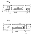
Mit Bezug auf
Der Rahmen 216 ist als Bügel oder Tasche, die einen Raum oder Hohlraum 217 um die Sensorspule 214 definiert, ausgebildet. Am stärksten bevorzugt ist der Rahmen 216 ein aus Kunststoff gefertigtes separates, eigenständiges Teil und umfasst einen die Sensorspule 214 umgebenden Abstützbügel 216, an dessen Oberseite sich ein Überbrückungsabschnitt 216a befindet, der an einem Ort, der einen Tastschalter an der Benutzerschnittstelle der Frontplatte 218 definiert, über der Sensorspule 214 und unter der Abdeckung 218, an die Unterseite der Abdeckung 218 angrenzend und in Kontakt mit dieser, verläuft. An die Unterseite des Überbrückungsabschnitts 216a ist im Hohlraum 217 über der Sensorspule 214 ein metallisches Target 212 dieser Ausführungsform geheftet. Der Abstützbügel 216 kann als Rahmen (d. h. vier Füße oder vier Wände usw.) gefertigt sein oder in Form eines Rings, der durch den Überbrückungsabschnitt 216a abgedeckt ist, vorliegen. Dieser Rahmen kann durch Schrauben, warm eingesetzte Verbinder oder andere herkömmliche Verbindungsverfahren mit der PCB 216 verbunden sein. In dieser Ausführungsform ist der Überbrückungsabschnitt 216a aus sehr dünnem Kunststoff entworfen, so dass die Durchbiegung der Abdeckung 218 zu einer Durchbiegung des Überbrückungsabschnitts 216a führt. In einem speziellen Beispiel beträgt die Dicke "A" des Überbrückungsabschnitts 216a 0,8 mm.The
Auf die Durchbiegung der Abdeckung 218 und daraus resultierend des Überbrückungsabschnitts 216a hin wird auch das metallische Target 212 an der Unterseite des Überbrückungsabschnitts durchgebogen, womit sich zwischen dem Target 212 und der Sensorspule 214 verändert, was ein Drücken des Tastschalters anzeigt. Somit ist bei dieser Ausführungsform das Target 212 durch eine Struktur unterstützt, die zwischen der Frontplattenabdeckung 218 und der PCB 219 angeordnet ist, und nicht direkt an die Unterseite der Frontplattenabdeckung 218 geheftet.Upon deflection of the
Wie oben angemerkt worden ist, ist das Target 212 der Tastschalteranordnung 200 stattdessen an die Unterseite des Überbrückungsabschnitts 216a geheftet, um das Target 212 in die gewünschte Beziehung mit der Sensorspule 214 zu bringen. In einer besonderen Ausführungsform der vorliegenden Erfindung ist das Target 212 als Teil eines Heißprägeprozesses an der Unterseite des Überbrückungsabschnitts angebracht. Alternativ kann nach Bedarf das Target 212 durch Drucken des Targets direkt auf die Rückseite der Abdeckung, um eine Metalloberfläche über der Sensorspule zu schaffen, an der Unterseite des Überbrückungsabschnitts 216a angebracht sein. Beispielsweise kann in Übereinstimmung mit dieser Ausführungsform eine heißgeprägte Folie oder ein leitendes Druckmaterial durch einen geeigneten Prozess (d. h. Heißprägen, Drucken usw.) auf den Rahmen 216 aufgebracht sein. Das Heißprägen oder Drucken des Targets 212 auf eine Oberfläche des Rahmens 216 anstatt die Abdeckung 218 kann speziell bei Anwendungen, bei denen eine benachbarte Beleuchtung benötigt wird und/oder gekrümmte Oberflächen verwendet werden, sinnvoll sein.As noted above, the
In einer besonderen Ausführungsform der Erfindung definiert ein Abschnitt der Frontplatte 218 eine Benutzerschnittstelle oder Tastatur für ein Produkt oder Haushaltsgerät. Unter Anwendung eines Heißprägeprozesses wird eine Metallfolie auf die innere Oberfläche des Kunststoffbügels oder der Kunststofftasche geprägt. Bei dieser Ausführungsform besitzt die Folie wünschenswerter weise eine Dicke zwischen 0,05 mm und 0,1 mm. Somit sind bei dieser Ausführungsform die herkömmlichen PCB-basierten Tastenblöcke durch eine heißgeprägte Folie oder gedruckte leitende Schicht, die durch einen separaten Bügel unterstützt ist, ersetzt.In a particular embodiment of the invention, a portion of the
Alternativ, wie oben beschrieben worden ist, kann ein Druckprozess angewandt werden, um ein leitendes Material auf die Unterseite des Überbrückungsabschnitts 216a zu drucken. Die Dicke des gedruckten Materials wäre ähnlich zu jener für die heißgeprägte Folie, d. h. betrüge am stärksten bevorzugt zwischen 0,05 mm und 0,1 mm.Alternatively, as described above, a printing process may be used to apply a conductive material to the underside of the
In
In einer in
Wie bei der Tastschalteranordnung 200 kann das Target 212 der Tastschalteranordnung 220 auf verschiedene Art und Weise einschließlich, jedoch nicht darauf beschränkt, durch Heißprägen des Targets 212 auf den Rahmen 226 und/oder Drucken des Targets 212 auf den Rahmen 226 unter Verwendung einer leitenden Tinte am Rahmen 226 angebracht sein. Es sei angemerkt, dass nach Bedarf das Target 212 auch als Metallscheibe oder -folie ausgebildet sein kann, die an der Unterseite des Überbrückungsabschnitts 226a haftend angebracht ist, ohne vom Leitgedanken der vorliegenden Erfindung abzuweichen.As with the
In
Der Rahmen 310 umfasst außerdem einen Schubstift oder Wulst 310b, der sich von der Mitte des Überbrückungsabschnitts 310a zur Sensorspule 320 hin erstreckt. Bei dieser Ausführungsform der Erfindung steht das Target 330 mit dem fernen Ende des Wulstes 310b in Verbindung und besitzt einen Umfang, der größer ist als der Umfang der Sensorspule 320, so dass er die Sensorspule 320 umschreibt. Wie ersichtlich ist, bewirkt eine Durchbiegung der Frontplatte 318 über dem Überbrückungsabschnitt 310a, dass der Schubstift 310b einen Abschnitt des Targets 330 schiebt, somit das Target 330 durchbiegt und die Kopplung zwischen dem Target 330 und der Sensorspule 320 verändert, was ein Drücken des Tastschalters anzeigt. Bei der Ausführungsform nach
Es sei angemerkt, dass in Verbindung mit dem Rahmen 310 andere Formeln eines Targets verwendet werden können, um dieselben Ergebnisse zu erzielen. Beispielsweise zeigen die
Ähnlich kann, um nun auf die
In
Außerdem können nach Bedarf die LEDs 330 durch LEDs ersetzt werden, die an der Vorderseite der PCB 355 montiert sind. In den
In
Außerdem können in Übereinstimmung mit den in Verbindung mit
In
In den
Jedes Tastschalterelement 640 ist so entworfen, dass es mit einer Öffnung 620a des Rahmens 620 zusammenpasst, wobei die Licht übertragenden Vorwölbungen 640 durch die Frontplatte 610 der Anordnung 600 gehen. Eine ebene Außenfläche 640c des Tastschalterelements 640 ist dazu vorgesehen, eine Haftschicht und/oder die Frontplatte 610 zu unterstützen. Das Tastschalterelement 640 ist durch die Nasen 640b und die Nut 640e, die die Rückseite des Rahmens 620, d. h. die von der vorderen Außenfläche 610 ferne Seite, in Eingriff nehmen, im Rahmen gehalten (wie in
Nach der Montage ist jedes Tastschalterelement 640 über einer Sensorspule durch den Rahmen 620 und/oder eine Haftschicht 612 (die nicht unter den Abschnitt des Tastschalterelements 640, das das Target umfasst, führt) unterstützt. Das Target an der rückwärtigen Außenfläche 640d jedes Tastschalterelements 640 ist in der gewünschten Beziehung mit einer Sensorspule angeordnet, wie anderswo hier beschrieben worden ist. Somit führt das Drücken der über einem Tastschalterelement 640 befindlichen vorderen Außenfläche oder Abdeckung zu einer Durchbiegung des Tastschalterelements 640, womit die Kopplung zwischen einem Target an der untersten Außenfläche 640d des Tastschalterelements 640 und dem Target verändert wird.After assembly, each
Es ist wichtig anzumerken, dass die in Verbindung mit den
Obwohl die Erfindung hier als in einem induktiven Sensortastschalter, seiner Anordnung und seiner Schaltung konkretisiert veranschaulicht und beschrieben worden ist, soll sie dennoch nicht nur auf die gezeigten Details beschränkt sein. Beispielsweise kann die induktive Tastschaltung der vorliegenden Erfindung so modifiziert sein, dass sie eine Referenzspule umfasst, die an einer Tastenposition der Tastatur ausgeführt ist. Bei einer solchen Konfiguration wird die Referenzspule verwendet, um die Driftkompensation als Standardreferenz, wobei keine Tastenbewegung erlaubt ist, zu unterstützen. Wie ersichtlich ist, können ohne Abweichung vom Leitgedanken der Erfindung die lediglich durch die zugefügten Ansprüche definiert wird, und im Umfang und Bereich von Entsprechungen der Ansprüche liegend verschiedene Modifikationen und konstruktive Veränderungen daran vorgenommen werden können.While the invention has been illustrated and described in detail herein as being in and for inclusion in an inductive sensor load switch, it is not intended to be limited solely to the details shown. For example, the inductive keying circuit of the present invention may be modified to include a reference coil implemented at a key position of the keyboard. In such a configuration, the reference coil is used to provide drift compensation as a standard reference, with no key movement is allowed to assist. As will be appreciated, without departing from the scope of the invention, which is defined solely by the appended claims, and various modifications and changes in design may be made therein in the scope and scope of equivalents of the claims.
Claims (19)
- Arrangement for an inductive sensor touch switch, which arrangement comprises:a user interface front panel section (18, 218, 218', 318, 457, 610);a sensor coil (14, 26, 110, 110a, 162, 214, 320, 510, 515, 520, 530, 540, 550) which is arranged on a printed circuit board (19, 219, 229, 302, 355, 415, 445, 555, 630);a conductive target (12, 212, 330, 332, 334, 338, 510, 570) which is arranged between the user interface front panel section (18, 218, 218', 318, 457, 610) and the sensor coil (14, 26, 110, 110a, 162, 214, 320, 510, 515, 520, 530, 540, 550);a frame (216, 226, 310, 350, 420, 440, 560, 620) which is arranged between the printed circuit board (19, 219, 229, 302, 355, 415, 445, 555, 630) and the user interface front panel section (18, 218, 218', 318, 457, 610), characterized in that the frame (216, 226, 310, 350, 420, 440, 560, 620) comprises a bridging section (216a, 226a, 310a) which has an uppermost surface, which is adjacent to the lower surface of the user interface front panel section (18, 218, 218', 318, 457, 610), and a lowermost surface, which faces the sensor coil (14, 26, 110, 110a, 162, 214, 320, 510, 515, 520, 530, 540, 550), and wherein the conductive target (12, 212, 330, 332, 334, 338, 510, 570) is arranged closest to the lowermost surface of the bridging section (216a, 226a, 310a), as a result of which a deflection of the front panel section (18, 218, 218', 318, 457, 610) above the frame (216, 226, 310, 350, 420, 440, 560, 620) leads to a deflection of the bridging section (216a, 226a, 310a) and a movement of at least one section of the conductive target (12, 212, 330, 332, 334, 338, 510, 570) in the direction of the sensor coil (14, 26, 110, 110a, 162, 214, 320, 510, 515, 520, 530, 540, 550).
- Arrangement according to Claim 1, characterized in that a system (100) has a plurality of arrangements for an inductive sensor touch switch (200, 220, 300, 340, 400, 430, 500, 550, 600), wherein each sensor coil (14, 26, 110, 110a, 162, 214, 320, 510, 515, 520, 530, 540, 550) is connected directly to earth (112) by means of a common supply line connection.
- Arrangement according to Claim 1 or 2, characterized in that the arrangement (200, 220, 300, 340, 400, 430, 500, 550, 600) further comprises at least one light emitter (230, 330, 410, 450) which is arranged on the printed circuit board (19, 219, 229, 302, 355, 415, 445, 555, 630), and wherein at least one section of the frame (216, 226, 310, 350, 420, 440, 560, 620) is produced from a transparent material, wherein the transparent section of the frame (216, 226, 310, 350, 420, 440, 560, 620) is arranged such that it is optically connected to an emitting section of the at least one light emitter (230, 330, 410, 450).
- Arrangement according to one of the preceding claims, characterized in that the target (12, 212, 330, 332, 334, 338, 510, 570) is attached directly to the lowermost surface of the bridging section (216a, 226a, 310a).
- Arrangement according to Claim 4, characterized in that the conductive target (12, 212, 330, 332, 334, 338, 510, 570) is attached to the lowermost surface of the bridging section (216a, 226a, 310a) by hot-stamping and/or printing.
- Arrangement according to Claim 4, characterized in that the frame (216, 226, 310, 350, 420, 440, 560, 620) further comprises a bead section (310b, 350a, 560a) which protrudes from the bridging section (216a, 226a, 310a), wherein the conductive target (12, 212, 330, 332, 334, 338, 510, 570) is arranged at a distance from the bridging section (216a, 226a, 310a) such that it is connected to the bead section (310b, 350a, 560a).
- Arrangement according to Claim 6, characterized in that the conductive target (12, 212, 330, 332, 334, 338, 510, 570) is attached to the remote bead section (310b, 350a, 560a) and hovers above the sensor coil (14, 26, 110, 110a, 162, 214, 320, 510, 515, 520, 530, 540, 550).
- Arrangement according to Claim 6, characterized in that the conductive target (12, 212, 330, 332, 334, 338, 510, 570) is a conductive cap (330, 334) which is fitted between the printed circuit board (19, 219, 229, 302, 355, 415, 445, 555, 630) and the bead section (310b, 350a, 560a) and above the sensor coil (14, 26, 110, 110a, 162, 214, 320, 510, 515, 520, 530, 540, 550) on the printed circuit board (19, 219, 229, 302, 355, 415, 445, 555, 630).
- Arrangement according to Claim 1, characterized in that the sensor coil (14, 26, 110, 110a, 162, 214, 320, 510, 515, 520, 530, 540, 550) comprises a first set of turns (510, 540), which rotate in a first direction, and a second set of turns (520, 550), which rotate in a second direction, wherein the second direction is opposite to the first direction, wherein the second set of turns (520, 550) surrounds the first set of turns (510, 540).
- Arrangement according to Claim 1, characterized in that the sensor coil (14, 26, 110, 110a, 162, 214, 320, 510, 515, 520, 530, 540, 550) comprises a first set of turns (510), wherein the arrangement (200, 220, 300, 340, 400, 430, 500, 550, 600) further comprises at least one additional turn (520) which is arranged outside the first set of turns (510), wherein the at least one additional turn (520) is short-circuited to form a reference potential.
- Arrangement according to one of the preceding claims, characterized in that at least one sensor coil (14, 26, 110, 110a, 162, 214, 320, 510, 515, 520, 530, 540, 550) is a multi-plane sensor coil (530).
- System for an inductive sensor touch switch, which system comprises a plurality of arrangements for an inductive sensor touch switch (200, 220, 300, 340, 400, 430, 500, 550, 600) according to one of Claims 1 to 11, wherein each of the arrangements for the inductive sensor touch switch (200, 220, 300, 340, 400, 430, 500, 550, 600) comprises a conductive target (12, 212, 330, 332, 334, 338, 510, 570) which is coupled to a sensor coil (14, 26, 110, 110a, 162, 214, 320, 510, 515, 520, 530, 540, 550);
a plurality of driver circuits (120) which generate a driver current, wherein each of the plurality of driver circuits (120) comprises its own driver transistor (T1), and wherein each of the plurality of driver circuits (120) supplies a driver current only to one of the plurality of arrangements for inductive sensor touch switches (200, 220, 300, 340, 400, 430, 500, 550, 600). - System according to Claim 12, characterized in that each of the plurality of driver circuits (120) is arranged on the printed circuit board (19, 219, 229, 302, 355, 415, 445, 555, 630) locally to that arrangement for the inductive sensor touch switch (200, 220, 300, 340, 400, 430, 500, 550, 600) to which it supplies a driver current.
- System according to Claim 12 or 13, characterized in that at least one of the plurality of arrangements for an inductive sensor touch switch (200, 220, 300, 340, 400, 430, 500, 550, 600) comprises a front panel section (18, 218, 218', 318, 457, 610), wherein the conductive target (12, 212, 330, 332, 334, 338, 510, 570) is arranged adjacent to and at a distance from the sensor coil (14, 26, 110, 110a, 162, 214, 320, 510, 515, 520, 530, 540, 550) of the at least one arrangement for an inductive sensor touch switch (200, 220, 300, 340, 400, 430, 500, 550, 600), wherein the sensor coil (14, 26, 110, 110a, 162, 214, 320, 510, 515, 520, 530, 540, 550) is arranged on a printed circuit board (19, 219, 229, 302, 355, 415, 445, 555, 630).
- System according to Claim 14, characterized in that a second printed circuit board (565) is arranged between the printed circuit board (19, 219, 229, 302, 355, 415, 445, 555, 630) with the sensor coil (14, 26, 110, 110a, 162, 214, 320, 510, 515, 520, 530, 540, 550) and the front panel section (18, 218, 218', 318, 457, 610), and a frame (216, 226, 310, 350, 420, 440, 560, 620) is arranged between the second printed circuit board (565) and the front panel section (18, 218, 218', 318, 457, 610).
- System according to Claim 15, characterized in that the frame (216, 226, 310, 350, 420, 440, 560, 620) comprises the bridging section (216a, 226a, 310a) which has an uppermost surface, which is adjacent to a lower surface of the front panel section (18, 218, 218', 318, 457, 610), and a lowermost surface, which faces the second printed circuit board (565).
- System according to Claim 15 or 16, characterized in that the frame (216, 226, 310, 350, 420, 440, 560, 620) comprises a bead section (310b, 350a, 560a) which projects from the lowermost surface of the bridging section (216a, 226a, 310a), wherein the remote section of the bead section (310b, 350a, 560a) is arranged adjacent to a section of a front surface of the second printed circuit board (565) or such that it is connected to the said section.
- System according to Claim 17, characterized in that the conductive target (12, 212, 330, 332, 334, 338, 510, 570) is arranged on a section of a rear surface of the second printed circuit board (565) beneath the bead section (310b, 350a, 560a), so that a deflection of the front panel section (18, 218, 218', 318, 457, 610) above the frame (216, 226, 310, 350, 420, 440, 560, 620) leads to a deflection of the bridging section (216a, 226a, 310a), it being possible for the force of the said deflection to be transmitted to the second printed circuit board (565) by the bead section (310b, 350a, 560a), as a result of which the second printed circuit board (565) can be deflected and the coupling between the conductive target (12, 212, 330, 332, 334, 338, 510, 570) and the sensor coil (14, 26, 110, 110a, 162, 214, 320, 510, 515, 520, 530, 540, 550) can be varied.
- System according to one of the preceding claims, characterized in that each arrangement for the inductive sensor button (200, 220, 300, 340, 400, 430, 500, 550, 600) comprises a transparent touch-operated element which is supported by a frame (216, 226, 310, 350, 420, 440, 560, 620), wherein the target (12, 212, 330, 332, 334, 338, 510, 570) is arranged on a rear outer face of the transparent touch-operated element.
Priority Applications (2)
| Application Number | Priority Date | Filing Date | Title |
|---|---|---|---|
| PL11703823T PL2529484T3 (en) | 2010-01-29 | 2011-01-31 | Arrangement and system for an inductive sensor push-button |
| EP20130003703 EP2660980A2 (en) | 2010-01-29 | 2011-01-31 | Arrangement and system for an inductive sensor push-button |
Applications Claiming Priority (2)
| Application Number | Priority Date | Filing Date | Title |
|---|---|---|---|
| US12/696,458 US20110187204A1 (en) | 2010-01-29 | 2010-01-29 | Inductive touch key switch system, assembly and circuit |
| PCT/EP2011/000426 WO2011092033A2 (en) | 2010-01-29 | 2011-01-31 | Arrangement and system for an inductive sensor push-button |
Related Child Applications (1)
| Application Number | Title | Priority Date | Filing Date |
|---|---|---|---|
| EP13003703.9 Division-Into | 2013-07-24 |
Publications (2)
| Publication Number | Publication Date |
|---|---|
| EP2529484A2 EP2529484A2 (en) | 2012-12-05 |
| EP2529484B1 true EP2529484B1 (en) | 2013-12-25 |
Family
ID=44319893
Family Applications (2)
| Application Number | Title | Priority Date | Filing Date |
|---|---|---|---|
| EP20130003703 Withdrawn EP2660980A2 (en) | 2010-01-29 | 2011-01-31 | Arrangement and system for an inductive sensor push-button |
| EP20110703823 Not-in-force EP2529484B1 (en) | 2010-01-29 | 2011-01-31 | Arrangement and system for an inductive sensor push-button |
Family Applications Before (1)
| Application Number | Title | Priority Date | Filing Date |
|---|---|---|---|
| EP20130003703 Withdrawn EP2660980A2 (en) | 2010-01-29 | 2011-01-31 | Arrangement and system for an inductive sensor push-button |
Country Status (4)
| Country | Link |
|---|---|
| US (1) | US20110187204A1 (en) |
| EP (2) | EP2660980A2 (en) |
| PL (1) | PL2529484T3 (en) |
| WO (1) | WO2011092033A2 (en) |
Cited By (6)
| Publication number | Priority date | Publication date | Assignee | Title |
|---|---|---|---|---|
| DE102014007036A1 (en) | 2014-05-13 | 2015-11-19 | Diehl Ako Stiftung & Co. Kg | Operating device, in particular for an electronic household appliance |
| DE102014015003A1 (en) | 2014-10-09 | 2016-04-14 | Diehl Ako Stiftung & Co. Kg | Operating device, in particular for an electronic household appliance |
| DE102015009781A1 (en) | 2015-07-24 | 2017-01-26 | Diehl Ako Stiftung & Co. Kg | Operating device, in particular for an electronic household appliance |
| DE102015014245A1 (en) | 2015-11-04 | 2017-05-18 | Diehl Ako Stiftung & Co. Kg | Operating device, in particular for electronic household appliances |
| WO2017174097A1 (en) | 2016-04-07 | 2017-10-12 | Diehl Ako Stiftung & Co. Kg | Operator control apparatus, in particular for a domestic appliance |
| DE102016004220A1 (en) | 2016-04-07 | 2017-10-12 | Diehl Ako Stiftung & Co. Kg | Operating device, in particular for an electronic household appliance |
Families Citing this family (20)
| Publication number | Priority date | Publication date | Assignee | Title |
|---|---|---|---|---|
| US20120242515A1 (en) * | 2011-03-24 | 2012-09-27 | Diehl Ako Stiftung & Co. Kg | Inductive touch sensing circuit providing sensitivity compensation |
| DE102011075942A1 (en) * | 2011-05-16 | 2013-05-16 | E.G.O. Elektro-Gerätebau GmbH | Operating device for an electrical appliance and electrical appliance |
| WO2012166710A2 (en) * | 2011-05-27 | 2012-12-06 | Diehl Ako Stiftung & Co. Kg | Inductive touch key switch system including a deflection translation mechanism |
| US9214936B2 (en) * | 2013-06-18 | 2015-12-15 | Hyundai Motor Company | Non-contact sensing module and method of manufacturing the same |
| US10527457B2 (en) | 2015-02-27 | 2020-01-07 | Azoteq (Pty) Ltd | Inductance sensing |
| US9746168B1 (en) * | 2015-10-30 | 2017-08-29 | American Opto Plus Led Corporation | Light-emitting touch buttons |
| CN107204763A (en) * | 2016-03-17 | 2017-09-26 | 峰范(北京)科技有限公司 | Metal touch control key strcture |
| US10275055B2 (en) | 2016-03-31 | 2019-04-30 | Azoteq (Pty) Ltd | Rotational sensing |
| CN206043729U (en) * | 2016-06-30 | 2017-03-29 | 刘颂东 | Electronic product touch screen high sensitivity contactor control device in environment under water |
| US10495486B2 (en) * | 2016-12-26 | 2019-12-03 | Texas Instruments Incorporated | Inductive touch input |
| CN111094901A (en) | 2017-07-13 | 2020-05-01 | 阿佐特克(私人)有限公司 | Inductive sensing user interface device |
| KR101954368B1 (en) * | 2017-08-31 | 2019-03-05 | (주)실리콘인사이드 | Mutual inductive force sensor module for 3d touch implementation |
| US10255020B1 (en) * | 2017-11-28 | 2019-04-09 | Ultravision Technologies, Llc | Multi-panel display having board-to-board interfaces between adjacent panels |
| GB2570533B (en) * | 2017-12-20 | 2021-09-22 | Sonuus Ltd | Keyboard sensor systems and methods |
| GB2578346B (en) | 2018-08-07 | 2021-03-03 | Sonuus Ltd | Computer input devices |
| KR102315414B1 (en) * | 2019-07-18 | 2021-10-21 | 주식회사 다모아텍 | Touch force sensor using inductive sensing and capacitive sensing and method of operation thereof |
| TWI731409B (en) * | 2019-09-09 | 2021-06-21 | 國立清華大學 | Micro tactility simulating sensing device and method to produce the device |
| WO2021081570A1 (en) | 2019-10-22 | 2021-04-29 | Azoteq (Pty) Ltd | Electronic device user interface |
| WO2023139416A1 (en) * | 2022-01-24 | 2023-07-27 | Sateco Ag | An assembly suitable for use in a button/switch assembly |
| CN114273269B (en) * | 2022-03-02 | 2022-06-03 | 宁波长晟电子科技有限公司 | Detection equipment for automobile key identification induction coil |
Family Cites Families (5)
| Publication number | Priority date | Publication date | Assignee | Title |
|---|---|---|---|---|
| US4838139A (en) * | 1986-03-18 | 1989-06-13 | Sensor Technologies, Inc. | Musical keyboard |
| ATE439630T1 (en) * | 2006-07-22 | 2009-08-15 | Darran Kreit | PRESSURE SENSITIVE INDUCTIVE DETECTOR FOR USE IN USER SURFACES |
| GB2446702A (en) * | 2007-02-13 | 2008-08-20 | Qrg Ltd | Touch Control Panel with Pressure Sensor |
| US8408723B2 (en) * | 2009-09-01 | 2013-04-02 | Microchip Technology Incorporated | Backlighting inductive touch buttons |
| US20110084933A1 (en) * | 2009-10-08 | 2011-04-14 | Microchip Technology Incorporated | Laminated printed circuit board inductive touch sensor |
-
2010
- 2010-01-29 US US12/696,458 patent/US20110187204A1/en not_active Abandoned
-
2011
- 2011-01-31 PL PL11703823T patent/PL2529484T3/en unknown
- 2011-01-31 EP EP20130003703 patent/EP2660980A2/en not_active Withdrawn
- 2011-01-31 WO PCT/EP2011/000426 patent/WO2011092033A2/en active Application Filing
- 2011-01-31 EP EP20110703823 patent/EP2529484B1/en not_active Not-in-force
Cited By (8)
| Publication number | Priority date | Publication date | Assignee | Title |
|---|---|---|---|---|
| DE102014007036A1 (en) | 2014-05-13 | 2015-11-19 | Diehl Ako Stiftung & Co. Kg | Operating device, in particular for an electronic household appliance |
| WO2015172863A1 (en) | 2014-05-13 | 2015-11-19 | Diehl Ako Stiftung & Co. Kg | Operating device, in particular for an electronic household appliance |
| DE102014007036B4 (en) * | 2014-05-13 | 2017-07-27 | Diehl Ako Stiftung & Co. Kg | Operating device, in particular for an electronic household appliance |
| DE102014015003A1 (en) | 2014-10-09 | 2016-04-14 | Diehl Ako Stiftung & Co. Kg | Operating device, in particular for an electronic household appliance |
| DE102015009781A1 (en) | 2015-07-24 | 2017-01-26 | Diehl Ako Stiftung & Co. Kg | Operating device, in particular for an electronic household appliance |
| DE102015014245A1 (en) | 2015-11-04 | 2017-05-18 | Diehl Ako Stiftung & Co. Kg | Operating device, in particular for electronic household appliances |
| WO2017174097A1 (en) | 2016-04-07 | 2017-10-12 | Diehl Ako Stiftung & Co. Kg | Operator control apparatus, in particular for a domestic appliance |
| DE102016004220A1 (en) | 2016-04-07 | 2017-10-12 | Diehl Ako Stiftung & Co. Kg | Operating device, in particular for an electronic household appliance |
Also Published As
| Publication number | Publication date |
|---|---|
| EP2529484A2 (en) | 2012-12-05 |
| WO2011092033A2 (en) | 2011-08-04 |
| US20110187204A1 (en) | 2011-08-04 |
| EP2660980A2 (en) | 2013-11-06 |
| PL2529484T3 (en) | 2014-07-31 |
| WO2011092033A3 (en) | 2011-10-27 |
Similar Documents
| Publication | Publication Date | Title |
|---|---|---|
| EP2529484B1 (en) | Arrangement and system for an inductive sensor push-button | |
| EP1760886B1 (en) | Sensor device | |
| DE60305034T2 (en) | KEYBOARDS AND PUSHBUTTONS | |
| DE102007003271A1 (en) | Keyboard arrangement and mobile terminal equipped therewith | |
| EP2455959B1 (en) | Switching device for a medical appliance and method for operating switching device | |
| EP2067257B1 (en) | Input unit for electrotechnical devices | |
| EP3084961A1 (en) | Contact and/or proximity-sensitive input device | |
| EP2061276A1 (en) | Hearing aid | |
| EP2197115A1 (en) | Operating device with at least one pressure switch | |
| EP2355356A1 (en) | Capacitative touch and/or proximity sensor | |
| DE102014007036B4 (en) | Operating device, in particular for an electronic household appliance | |
| EP3049288B1 (en) | Assembly for operating a vehicle function | |
| EP3440773B1 (en) | Operator control apparatus, in particular for a domestic appliance | |
| DE102014106677A1 (en) | Manual operation for an electromotive furniture drive, method for detecting actuation of a manual operation, and an electromotive furniture drive | |
| DE102018002046A1 (en) | ELECTRONIC MUSICAL INSTRUMENT AND KEYBOARD DEVICE | |
| EP2348638B1 (en) | Capacitive contact and/or proximity switch | |
| EP3472936A1 (en) | Device having at least one region that can be illuminated | |
| DE102016004220B4 (en) | Operating device, in particular for an electronic household appliance | |
| DE102008021943A1 (en) | Electrical device i.e. cooking hob, has capacitive control device provided with transparent carrier plate, where upper side of carrier plate is attached to lower side of glass plate by transparent adhesive i.e. adhesive foil | |
| DE202008014509U1 (en) | Evenly lit keyboard device | |
| DE102011079737A1 (en) | Operating device for a household appliance and household appliance | |
| DE102008014463A1 (en) | Control unit for ventilation and/or air conditioning system of vehicle, has projection with region formed as capacitively acting electrode, and feed pipe guided into electrode, where pipe is electrically connected with plate contact field | |
| DE102014015003A1 (en) | Operating device, in particular for an electronic household appliance | |
| DE102015014245A1 (en) | Operating device, in particular for electronic household appliances | |
| DE202013011515U1 (en) | Touch and / or proximity sensitive input device |
Legal Events
| Date | Code | Title | Description |
|---|---|---|---|
| PUAI | Public reference made under article 153(3) epc to a published international application that has entered the european phase |
Free format text: ORIGINAL CODE: 0009012 |
|
| 17P | Request for examination filed |
Effective date: 20120623 |
|
| AK | Designated contracting states |
Kind code of ref document: A2 Designated state(s): AL AT BE BG CH CY CZ DE DK EE ES FI FR GB GR HR HU IE IS IT LI LT LU LV MC MK MT NL NO PL PT RO RS SE SI SK SM TR |
|
| DAX | Request for extension of the european patent (deleted) | ||
| REG | Reference to a national code |
Ref country code: DE Ref legal event code: R079 Ref document number: 502011001883 Country of ref document: DE Free format text: PREVIOUS MAIN CLASS: H03K0017960000 Ipc: H03K0017970000 |
|
| RIC1 | Information provided on ipc code assigned before grant |
Ipc: H03K 17/96 20060101ALI20130530BHEP Ipc: H03K 17/97 20060101AFI20130530BHEP |
|
| GRAP | Despatch of communication of intention to grant a patent |
Free format text: ORIGINAL CODE: EPIDOSNIGR1 |
|
| INTG | Intention to grant announced |
Effective date: 20130712 |
|
| GRAS | Grant fee paid |
Free format text: ORIGINAL CODE: EPIDOSNIGR3 |
|
| GRAA | (expected) grant |
Free format text: ORIGINAL CODE: 0009210 |
|
| AK | Designated contracting states |
Kind code of ref document: B1 Designated state(s): AL AT BE BG CH CY CZ DE DK EE ES FI FR GB GR HR HU IE IS IT LI LT LU LV MC MK MT NL NO PL PT RO RS SE SI SK SM TR |
|
| REG | Reference to a national code |
Ref country code: GB Ref legal event code: FG4D Free format text: NOT ENGLISH |
|
| REG | Reference to a national code |
Ref country code: CH Ref legal event code: EP |
|
| REG | Reference to a national code |
Ref country code: AT Ref legal event code: REF Ref document number: 647064 Country of ref document: AT Kind code of ref document: T Effective date: 20140115 |
|
| REG | Reference to a national code |
Ref country code: IE Ref legal event code: FG4D Free format text: LANGUAGE OF EP DOCUMENT: GERMAN |
|
| REG | Reference to a national code |
Ref country code: DE Ref legal event code: R096 Ref document number: 502011001883 Country of ref document: DE Effective date: 20140220 |
|
| PG25 | Lapsed in a contracting state [announced via postgrant information from national office to epo] |
Ref country code: FI Free format text: LAPSE BECAUSE OF FAILURE TO SUBMIT A TRANSLATION OF THE DESCRIPTION OR TO PAY THE FEE WITHIN THE PRESCRIBED TIME-LIMIT Effective date: 20131225 Ref country code: SE Free format text: LAPSE BECAUSE OF FAILURE TO SUBMIT A TRANSLATION OF THE DESCRIPTION OR TO PAY THE FEE WITHIN THE PRESCRIBED TIME-LIMIT Effective date: 20131225 Ref country code: LT Free format text: LAPSE BECAUSE OF FAILURE TO SUBMIT A TRANSLATION OF THE DESCRIPTION OR TO PAY THE FEE WITHIN THE PRESCRIBED TIME-LIMIT Effective date: 20131225 Ref country code: NO Free format text: LAPSE BECAUSE OF FAILURE TO SUBMIT A TRANSLATION OF THE DESCRIPTION OR TO PAY THE FEE WITHIN THE PRESCRIBED TIME-LIMIT Effective date: 20140325 Ref country code: HR Free format text: LAPSE BECAUSE OF FAILURE TO SUBMIT A TRANSLATION OF THE DESCRIPTION OR TO PAY THE FEE WITHIN THE PRESCRIBED TIME-LIMIT Effective date: 20131225 |
|
| REG | Reference to a national code |
Ref country code: NL Ref legal event code: VDEP Effective date: 20131225 |
|
| REG | Reference to a national code |
Ref country code: LT Ref legal event code: MG4D |
|
| PG25 | Lapsed in a contracting state [announced via postgrant information from national office to epo] |
Ref country code: LV Free format text: LAPSE BECAUSE OF FAILURE TO SUBMIT A TRANSLATION OF THE DESCRIPTION OR TO PAY THE FEE WITHIN THE PRESCRIBED TIME-LIMIT Effective date: 20131225 Ref country code: RS Free format text: LAPSE BECAUSE OF FAILURE TO SUBMIT A TRANSLATION OF THE DESCRIPTION OR TO PAY THE FEE WITHIN THE PRESCRIBED TIME-LIMIT Effective date: 20131225 |
|
| BERE | Be: lapsed |
Owner name: DIEHL AKO STIFTUNG & CO. K.G. Effective date: 20140131 |
|
| PG25 | Lapsed in a contracting state [announced via postgrant information from national office to epo] |
Ref country code: EE Free format text: LAPSE BECAUSE OF FAILURE TO SUBMIT A TRANSLATION OF THE DESCRIPTION OR TO PAY THE FEE WITHIN THE PRESCRIBED TIME-LIMIT Effective date: 20131225 Ref country code: IS Free format text: LAPSE BECAUSE OF FAILURE TO SUBMIT A TRANSLATION OF THE DESCRIPTION OR TO PAY THE FEE WITHIN THE PRESCRIBED TIME-LIMIT Effective date: 20140425 |
|
| REG | Reference to a national code |
Ref country code: PL Ref legal event code: T3 |
|
| PG25 | Lapsed in a contracting state [announced via postgrant information from national office to epo] |
Ref country code: LU Free format text: LAPSE BECAUSE OF FAILURE TO SUBMIT A TRANSLATION OF THE DESCRIPTION OR TO PAY THE FEE WITHIN THE PRESCRIBED TIME-LIMIT Effective date: 20140131 Ref country code: CY Free format text: LAPSE BECAUSE OF FAILURE TO SUBMIT A TRANSLATION OF THE DESCRIPTION OR TO PAY THE FEE WITHIN THE PRESCRIBED TIME-LIMIT Effective date: 20131225 Ref country code: RO Free format text: LAPSE BECAUSE OF FAILURE TO SUBMIT A TRANSLATION OF THE DESCRIPTION OR TO PAY THE FEE WITHIN THE PRESCRIBED TIME-LIMIT Effective date: 20131225 Ref country code: ES Free format text: LAPSE BECAUSE OF FAILURE TO SUBMIT A TRANSLATION OF THE DESCRIPTION OR TO PAY THE FEE WITHIN THE PRESCRIBED TIME-LIMIT Effective date: 20131225 Ref country code: PT Free format text: LAPSE BECAUSE OF FAILURE TO SUBMIT A TRANSLATION OF THE DESCRIPTION OR TO PAY THE FEE WITHIN THE PRESCRIBED TIME-LIMIT Effective date: 20140428 Ref country code: NL Free format text: LAPSE BECAUSE OF FAILURE TO SUBMIT A TRANSLATION OF THE DESCRIPTION OR TO PAY THE FEE WITHIN THE PRESCRIBED TIME-LIMIT Effective date: 20131225 Ref country code: CZ Free format text: LAPSE BECAUSE OF FAILURE TO SUBMIT A TRANSLATION OF THE DESCRIPTION OR TO PAY THE FEE WITHIN THE PRESCRIBED TIME-LIMIT Effective date: 20131225 Ref country code: SK Free format text: LAPSE BECAUSE OF FAILURE TO SUBMIT A TRANSLATION OF THE DESCRIPTION OR TO PAY THE FEE WITHIN THE PRESCRIBED TIME-LIMIT Effective date: 20131225 |
|
| REG | Reference to a national code |
Ref country code: CH Ref legal event code: PL |
|
| REG | Reference to a national code |
Ref country code: DE Ref legal event code: R097 Ref document number: 502011001883 Country of ref document: DE |
|
| PG25 | Lapsed in a contracting state [announced via postgrant information from national office to epo] |
Ref country code: MC Free format text: LAPSE BECAUSE OF FAILURE TO SUBMIT A TRANSLATION OF THE DESCRIPTION OR TO PAY THE FEE WITHIN THE PRESCRIBED TIME-LIMIT Effective date: 20131225 |
|
| PG25 | Lapsed in a contracting state [announced via postgrant information from national office to epo] |
Ref country code: LI Free format text: LAPSE BECAUSE OF NON-PAYMENT OF DUE FEES Effective date: 20140131 Ref country code: DK Free format text: LAPSE BECAUSE OF FAILURE TO SUBMIT A TRANSLATION OF THE DESCRIPTION OR TO PAY THE FEE WITHIN THE PRESCRIBED TIME-LIMIT Effective date: 20131225 Ref country code: CH Free format text: LAPSE BECAUSE OF NON-PAYMENT OF DUE FEES Effective date: 20140131 |
|
| PLBE | No opposition filed within time limit |
Free format text: ORIGINAL CODE: 0009261 |
|
| REG | Reference to a national code |
Ref country code: FR Ref legal event code: ST Effective date: 20140930 |
|
| STAA | Information on the status of an ep patent application or granted ep patent |
Free format text: STATUS: NO OPPOSITION FILED WITHIN TIME LIMIT |
|
| REG | Reference to a national code |
Ref country code: IE Ref legal event code: MM4A |
|
| PG25 | Lapsed in a contracting state [announced via postgrant information from national office to epo] |
Ref country code: FR Free format text: LAPSE BECAUSE OF NON-PAYMENT OF DUE FEES Effective date: 20140225 |
|
| 26N | No opposition filed |
Effective date: 20140926 |
|
| REG | Reference to a national code |
Ref country code: DE Ref legal event code: R097 Ref document number: 502011001883 Country of ref document: DE Effective date: 20140926 |
|
| PG25 | Lapsed in a contracting state [announced via postgrant information from national office to epo] |
Ref country code: BE Free format text: LAPSE BECAUSE OF NON-PAYMENT OF DUE FEES Effective date: 20140131 Ref country code: IE Free format text: LAPSE BECAUSE OF NON-PAYMENT OF DUE FEES Effective date: 20140131 |
|
| PGFP | Annual fee paid to national office [announced via postgrant information from national office to epo] |
Ref country code: IT Payment date: 20150122 Year of fee payment: 5 Ref country code: DE Payment date: 20150325 Year of fee payment: 5 |
|
| PG25 | Lapsed in a contracting state [announced via postgrant information from national office to epo] |
Ref country code: SI Free format text: LAPSE BECAUSE OF FAILURE TO SUBMIT A TRANSLATION OF THE DESCRIPTION OR TO PAY THE FEE WITHIN THE PRESCRIBED TIME-LIMIT Effective date: 20131225 |
|
| PGFP | Annual fee paid to national office [announced via postgrant information from national office to epo] |
Ref country code: PL Payment date: 20150116 Year of fee payment: 5 |
|
| GBPC | Gb: european patent ceased through non-payment of renewal fee |
Effective date: 20150131 |
|
| PG25 | Lapsed in a contracting state [announced via postgrant information from national office to epo] |
Ref country code: GB Free format text: LAPSE BECAUSE OF NON-PAYMENT OF DUE FEES Effective date: 20150131 |
|
| PG25 | Lapsed in a contracting state [announced via postgrant information from national office to epo] |
Ref country code: MT Free format text: LAPSE BECAUSE OF FAILURE TO SUBMIT A TRANSLATION OF THE DESCRIPTION OR TO PAY THE FEE WITHIN THE PRESCRIBED TIME-LIMIT Effective date: 20131225 |
|
| PG25 | Lapsed in a contracting state [announced via postgrant information from national office to epo] |
Ref country code: SM Free format text: LAPSE BECAUSE OF FAILURE TO SUBMIT A TRANSLATION OF THE DESCRIPTION OR TO PAY THE FEE WITHIN THE PRESCRIBED TIME-LIMIT Effective date: 20131225 |
|
| PG25 | Lapsed in a contracting state [announced via postgrant information from national office to epo] |
Ref country code: BG Free format text: LAPSE BECAUSE OF FAILURE TO SUBMIT A TRANSLATION OF THE DESCRIPTION OR TO PAY THE FEE WITHIN THE PRESCRIBED TIME-LIMIT Effective date: 20131225 Ref country code: GR Free format text: LAPSE BECAUSE OF FAILURE TO SUBMIT A TRANSLATION OF THE DESCRIPTION OR TO PAY THE FEE WITHIN THE PRESCRIBED TIME-LIMIT Effective date: 20140326 |
|
| PG25 | Lapsed in a contracting state [announced via postgrant information from national office to epo] |
Ref country code: TR Free format text: LAPSE BECAUSE OF FAILURE TO SUBMIT A TRANSLATION OF THE DESCRIPTION OR TO PAY THE FEE WITHIN THE PRESCRIBED TIME-LIMIT Effective date: 20131225 Ref country code: HU Free format text: LAPSE BECAUSE OF FAILURE TO SUBMIT A TRANSLATION OF THE DESCRIPTION OR TO PAY THE FEE WITHIN THE PRESCRIBED TIME-LIMIT; INVALID AB INITIO Effective date: 20110131 |
|
| REG | Reference to a national code |
Ref country code: DE Ref legal event code: R119 Ref document number: 502011001883 Country of ref document: DE |
|
| PG25 | Lapsed in a contracting state [announced via postgrant information from national office to epo] |
Ref country code: DE Free format text: LAPSE BECAUSE OF NON-PAYMENT OF DUE FEES Effective date: 20160802 |
|
| PG25 | Lapsed in a contracting state [announced via postgrant information from national office to epo] |
Ref country code: IT Free format text: LAPSE BECAUSE OF NON-PAYMENT OF DUE FEES Effective date: 20160131 |
|
| REG | Reference to a national code |
Ref country code: AT Ref legal event code: MM01 Ref document number: 647064 Country of ref document: AT Kind code of ref document: T Effective date: 20160131 |
|
| PG25 | Lapsed in a contracting state [announced via postgrant information from national office to epo] |
Ref country code: AT Free format text: LAPSE BECAUSE OF NON-PAYMENT OF DUE FEES Effective date: 20160131 |
|
| PG25 | Lapsed in a contracting state [announced via postgrant information from national office to epo] |
Ref country code: PL Free format text: LAPSE BECAUSE OF NON-PAYMENT OF DUE FEES Effective date: 20160131 |
|
| PG25 | Lapsed in a contracting state [announced via postgrant information from national office to epo] |
Ref country code: MK Free format text: LAPSE BECAUSE OF FAILURE TO SUBMIT A TRANSLATION OF THE DESCRIPTION OR TO PAY THE FEE WITHIN THE PRESCRIBED TIME-LIMIT Effective date: 20131225 |
|
| PG25 | Lapsed in a contracting state [announced via postgrant information from national office to epo] |
Ref country code: AL Free format text: LAPSE BECAUSE OF FAILURE TO SUBMIT A TRANSLATION OF THE DESCRIPTION OR TO PAY THE FEE WITHIN THE PRESCRIBED TIME-LIMIT Effective date: 20131225 |