EP2528190A2 - Ac adapter and electronic apparatus unit - Google Patents
Ac adapter and electronic apparatus unit Download PDFInfo
- Publication number
- EP2528190A2 EP2528190A2 EP12162004A EP12162004A EP2528190A2 EP 2528190 A2 EP2528190 A2 EP 2528190A2 EP 12162004 A EP12162004 A EP 12162004A EP 12162004 A EP12162004 A EP 12162004A EP 2528190 A2 EP2528190 A2 EP 2528190A2
- Authority
- EP
- European Patent Office
- Prior art keywords
- adapter
- electronic apparatus
- voltage
- state
- output terminal
- Prior art date
- Legal status (The legal status is an assumption and is not a legal conclusion. Google has not performed a legal analysis and makes no representation as to the accuracy of the status listed.)
- Granted
Links
Images





Classifications
-
- H—ELECTRICITY
- H02—GENERATION; CONVERSION OR DISTRIBUTION OF ELECTRIC POWER
- H02M—APPARATUS FOR CONVERSION BETWEEN AC AND AC, BETWEEN AC AND DC, OR BETWEEN DC AND DC, AND FOR USE WITH MAINS OR SIMILAR POWER SUPPLY SYSTEMS; CONVERSION OF DC OR AC INPUT POWER INTO SURGE OUTPUT POWER; CONTROL OR REGULATION THEREOF
- H02M7/00—Conversion of AC power input into DC power output; Conversion of DC power input into AC power output
- H02M7/02—Conversion of AC power input into DC power output without possibility of reversal
- H02M7/04—Conversion of AC power input into DC power output without possibility of reversal by static converters
- H02M7/06—Conversion of AC power input into DC power output without possibility of reversal by static converters using discharge tubes without control electrode or semiconductor devices without control electrode
-
- H—ELECTRICITY
- H02—GENERATION; CONVERSION OR DISTRIBUTION OF ELECTRIC POWER
- H02J—ELECTRIC POWER NETWORKS; CIRCUIT ARRANGEMENTS OR SYSTEMS FOR SUPPLYING OR DISTRIBUTING ELECTRIC POWER; SYSTEMS FOR STORING ELECTRIC ENERGY
- H02J4/00—Circuit arrangements for mains or distribution networks not specified as AC or DC; Circuit arrangements for mains or distribution networks combining AC and DC sections or sub-networks
- H02J4/20—Networks integrating separated AC and DC power sections
- H02J4/25—Networks integrating separated AC and DC power sections for transfer of electric power between AC and DC networks, e.g. for supplying the DC section within a load from an AC mains system
-
- H—ELECTRICITY
- H02—GENERATION; CONVERSION OR DISTRIBUTION OF ELECTRIC POWER
- H02J—ELECTRIC POWER NETWORKS; CIRCUIT ARRANGEMENTS OR SYSTEMS FOR SUPPLYING OR DISTRIBUTING ELECTRIC POWER; SYSTEMS FOR STORING ELECTRIC ENERGY
- H02J7/00—Circuit arrangements for charging or discharging batteries or for supplying loads from batteries
- H02J7/02—Circuit arrangements for charging or discharging batteries or for supplying loads from batteries for charging batteries from AC mains by converters
-
- H—ELECTRICITY
- H02—GENERATION; CONVERSION OR DISTRIBUTION OF ELECTRIC POWER
- H02J—ELECTRIC POWER NETWORKS; CIRCUIT ARRANGEMENTS OR SYSTEMS FOR SUPPLYING OR DISTRIBUTING ELECTRIC POWER; SYSTEMS FOR STORING ELECTRIC ENERGY
- H02J7/00—Circuit arrangements for charging or discharging batteries or for supplying loads from batteries
- H02J7/02—Circuit arrangements for charging or discharging batteries or for supplying loads from batteries for charging batteries from AC mains by converters
- H02J7/04—Regulation of charging current or voltage
-
- H—ELECTRICITY
- H02—GENERATION; CONVERSION OR DISTRIBUTION OF ELECTRIC POWER
- H02J—ELECTRIC POWER NETWORKS; CIRCUIT ARRANGEMENTS OR SYSTEMS FOR SUPPLYING OR DISTRIBUTING ELECTRIC POWER; SYSTEMS FOR STORING ELECTRIC ENERGY
- H02J7/00—Circuit arrangements for charging or discharging batteries or for supplying loads from batteries
- H02J7/80—Circuit arrangements for charging or discharging batteries or for supplying loads from batteries including monitoring or indicating arrangements
-
- H—ELECTRICITY
- H02—GENERATION; CONVERSION OR DISTRIBUTION OF ELECTRIC POWER
- H02J—ELECTRIC POWER NETWORKS; CIRCUIT ARRANGEMENTS OR SYSTEMS FOR SUPPLYING OR DISTRIBUTING ELECTRIC POWER; SYSTEMS FOR STORING ELECTRIC ENERGY
- H02J7/00—Circuit arrangements for charging or discharging batteries or for supplying loads from batteries
- H02J7/865—Battery or charger load switching, e.g. concurrent charging and load supply
-
- H—ELECTRICITY
- H02—GENERATION; CONVERSION OR DISTRIBUTION OF ELECTRIC POWER
- H02J—ELECTRIC POWER NETWORKS; CIRCUIT ARRANGEMENTS OR SYSTEMS FOR SUPPLYING OR DISTRIBUTING ELECTRIC POWER; SYSTEMS FOR STORING ELECTRIC ENERGY
- H02J7/00—Circuit arrangements for charging or discharging batteries or for supplying loads from batteries
- H02J7/90—Regulation of charging or discharging current or voltage
-
- H—ELECTRICITY
- H02—GENERATION; CONVERSION OR DISTRIBUTION OF ELECTRIC POWER
- H02J—ELECTRIC POWER NETWORKS; CIRCUIT ARRANGEMENTS OR SYSTEMS FOR SUPPLYING OR DISTRIBUTING ELECTRIC POWER; SYSTEMS FOR STORING ELECTRIC ENERGY
- H02J7/00—Circuit arrangements for charging or discharging batteries or for supplying loads from batteries
- H02J7/90—Regulation of charging or discharging current or voltage
- H02J7/94—Regulation of charging or discharging current or voltage in response to battery current
-
- H—ELECTRICITY
- H02—GENERATION; CONVERSION OR DISTRIBUTION OF ELECTRIC POWER
- H02M—APPARATUS FOR CONVERSION BETWEEN AC AND AC, BETWEEN AC AND DC, OR BETWEEN DC AND DC, AND FOR USE WITH MAINS OR SIMILAR POWER SUPPLY SYSTEMS; CONVERSION OF DC OR AC INPUT POWER INTO SURGE OUTPUT POWER; CONTROL OR REGULATION THEREOF
- H02M1/00—Details of apparatus for conversion
- H02M1/36—Means for starting or stopping converters
Definitions
- the embodiments discussed herein are related to an AC adapter for converting an alternating current into a direct current and supplying the direct current to an electronic apparatus, and an electronic apparatus unit including the AC adapter and the electronic apparatus.
- an alternator such as a commercial power or the like supplied through a household outlet has been widely used.
- an electronic apparatus such as a computer or the like generally operates with the direct current. Accordingly, an AC adapter is used to convert an alternating current into a direct current and supply the direct current to an electronic apparatus (hereinafter, called "main device").
- the AC adapter has a different rated current, a different type, and the like depending on its size or the like. By these different features, power to be supplied becomes different. However, since it is not possible to determine the rated current, the different type, and the like of the AC adapter at a side of the main device, a relationship between the main device and the AC adapter has been fixed. Accordingly, there is no compatibility between models, or manufacturers, and the AC adapter has not been standardized between different models, or manufacturers.
- the state of the power supply may be one of the following states: (1) a state of conducting power supply only to charge an internal battery of the main device, (2) a state of conducting power supply only for an actual operation of the main device. Moreover, as a state in which the power consumption is great, the power supply may be in (3) a state of conducting power supplies for a charge of the internal battery and for an actual operation of the main device.
- the AC adapter supports all states by its possible power to supply.
- Japanese Laid-open Patent Application No. 2004-341592 discloses a system including the main device capable of detecting power supply capacity information of an external power source device.
- a terminal other than a regular terminal for supplying power is provided.
- detecting, in the main device a range in which a voltage supplied from a side of the main device is dropped due to a resistor provided at a side of an external power source, a power supply ability of the external device is detected.
- Japanese Laid-open Patent Application No. H07-143749 discloses an AC adapter which includes an oscillation part for generating a signal voltage of an oscillation frequency corresponding to a current value possible to supply, and the signal voltage is superimposed with an original DC voltage.
- an operation state of the main device is changed by separating the signal voltage from the original voltage and measuring the signal voltage.
- Japanese Laid-open Patent Application No. H05-184065 discloses that connections of various types of power sources such as an AC adapter, an external battery, and the like are assumed, and the main device determines which type of the power source is connected based on the power voltage. In the main device, based on the determined type of the power source, the power consumption is adjusted in one of the above states (1) to (3).
- Japanese Laid-open Patent Application No. 2000-134816 discloses a system in which when the AC adapter is connected, an impedance on a power source output line is changed in a certain time, and a power source input specification of the main device itself is informed to the AC adapter.
- the AC adapter which is disclosed in Japanese Laid-open Patent Application No. 2000-134816 , generates the power source for an operation based on the informed power source input specification.
- the AC adapter since the AC adapter generates the power source for the operation of the AC adapter based on the specification of the main device, as a result, the AC adapter depends on the specification of the main device. Accordingly, it is not possible for the AC adapter including the above described mechanism to connect to the main device, and the main device does not allow AC adapters which are based on various specifications.
- the present disclosure aims at providing an AC adapter which improves compatibility, and an electronic apparatus unit using the AC adapter.
- an AC adapter including a conversion part configured to convert alternating current input to an input terminal into a direct current; an output terminal configured to supply the direct current to an electronic apparatus outside; and a voltage adjusting circuit configured to lower a voltage of the output terminal by a predetermined voltage from a regular supply voltage in a term after the AC adapter is connected to the electronic apparatus until a predetermined time lapses.
- FIG. 1 is an outline diagram illustrating a state in which the AC adapter 1 according to the first embodiment is connected to the electronic apparatus 101.
- the AC adapter 1 in the AC adapter 1 (or an AC adapter 2 described later in a second embodiment), one contact 10 as a plug-in is connected to an AC outlet 10a for household use, and another contact 20 as a terminal is connected to an input terminal 110 of the electronic apparatus 101.
- the electronic apparatus 101 may be regarded as a laptop personal computer, and functions as the main device using the AC adapter 1 or 2.
- Other examples of the electronic apparatus 101, a desktop personal computer, an Audio Visual (AV) device such as a television and a game machine, a portable television, and the like may be used.
- AV Audio Visual
- FIG. 2 is a diagram illustrating a circuit configuration of the AC adapter 1 according to the first embodiment.
- the AC adapter 1 includes the contact 10 being an input terminal as the plug, the contact 20 being an output terminal, a transformer 30, a rectification-smoothing circuit 35, and a voltage adjusting circuit 40.
- the transformer 30 may lower an alternating current input to the contact 10 to AC 19/ ( ⁇ 2) [V].
- the alternating current input to the contact 10 may be regarded as power of AC 100 [V] for a commercial use.
- the rectification-smoothing circuit 35 includes a diode 36, a capacitor 37, and the like.
- the rectification-smoothing circuit 35 converts the alternating current output from the transformer 30 into the direct current, and outputs the direct current to a side of the voltage adjusting circuit 40.
- a configuration of the rectification-smoothing circuit 35 illustrated in FIG. 2 is an example. Another configuration including a bridge circuit or the like may be applied.
- the voltage adjusting circuit 40 may be formed by a time-limit operation circuit, and includes a resistors 41A, 41B, 41C, 41D, and 41E, a P-channel Field Effect Transistor(FET) 42, a transistors 43A, 43B, and 43C, and a capacitor 44.
- the voltage adjusting circuit 40 lowers a voltage of the connector 20 in a predetermined time T1 after the AC adapter 1 is connected to the electronic apparatus 101, from a regular supply voltage Vn (which may be 19 [V]) to a predetermined voltage Vh.
- the resistor 41A is regarded as an output impedance element for determining the predetermined voltage Vh.
- the predetermined voltage Vh represents an information value for sending information of the specification of the AC adapter 1 to a side of the electronic apparatus 101.
- the information of the specification may indicate suppliable current, and may include information of an output voltage, a product number, a manufacturer, and the like. Details will be described later.
- the P-channel FET 42 changes from an OFF state to an ON state when the predetermined time T1 passes after the AC adapter 1 is connected to the electronic apparatus 101.
- the current flows to the contact 20 through the P-channel FET 42, a voltage in the contact 20 rises to the regular supply voltage Vn.
- FIG. 3 is a diagram illustrating the state change of each of the components of the AC adapter 1 in a term after the AC adapter 1 is connected to the AC outlet 10a and is mounted to the electronic apparatus 101 and until power supply starts to the electronic apparatus 101.
- the voltage in the contact 20 rises to the regular supply voltage Vn.
- the contact 20 is connected to the electronic apparatus 101 (time t2)
- the current flows from the AC adapter 1 to the electronic apparatus 101, and a state of the transistor 43A changes from the OFF state to the ON state in response to a voltage drop.
- the transistor 43A is in the ON state, the current, which is determined based on resistance values of the resistors 41A and 41B, flows into the capacitor 44, and the capacitor 44 is charged.
- the predetermined time T1 passes from the time t2.
- a charging voltage of the capacitor 44 becomes higher than a certain voltage Vbe (time t3)
- the transistor 43C changes from the OFF state to the ON state, and lowers a gate voltage of the P-channel FET 42 to 0 [V].
- the P-channel FET 42 changes from the OFF state to the ON state, and the voltage of the contact 20 rises to the regular supply voltage Vn.
- the state of transistor 43C becomes the ON state
- the state of the transistor 43B becomes the ON state
- a base current of the transistor 43C is supplied. Accordingly, the transistor 43C is retained in the ON state.
- the capacitor 44 is charged.
- the charging voltage becomes a certain voltage Vbe after a certain time lapses
- the transistor 43C is retained in the ON state.
- the voltage of the contact 20 rises to the regular supply voltage Vn, and the power supply starts to the electronic apparatus 101.
- the predetermined voltage Vh By appropriately selecting the resistance value of the resistor 41A, it is possible to realize the predetermined voltage Vh.
- the predetermined voltage Vh based on the specification of the AC adapter 1, it is possible to send the information of the specification of the AC adapter 1 to the electronic apparatus 101. Also, the number of terminals is not increased to send the information of the specification. It is possible to suppress increasing the expense and the size of the AC adapter 1.
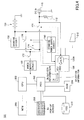
- FIG. 4 is a diagram illustrating an example of a circuit configuration of the electronic apparatus 101.
- the electronic apparatus 101 includes the input terminal 110, a pull-down resistor 112, an EC (Enabled Controller)/KBC (Keyboard Controller) 120, a battery 130, a standing power supply circuit 140, a charging circuit 150, and a power supply circuit 160. Switches 170, 172, 174, and 176 are provided among components.
- the EC/KBC 120 internally mounts a Central Processing Unit (CPU) and an A/D convertor 120A, and controls a pointing device such as a keyboard (KB), a mouse, and the like. Also, the EC/KBC 120 conducts various processes using its processing ability, and is operated by the power supply from the standing power supply circuit 140 which is an independent power supply circuit.
- CPU Central Processing Unit
- A/D convertor 120A controls a pointing device such as a keyboard (KB), a mouse, and the like.
- KB keyboard
- the EC/KBC 120 conducts various processes using its processing ability, and is operated by the power supply from the standing power supply circuit 140 which is an independent power supply circuit.
- FIG. 5 is a diagram illustrating a circuit configuration example of the standing power supply circuit 140.
- the standing power supply circuit 140 operates as a power supply circuit which outputs a lower current always being supplied.
- the standing power supply circuit 140 may be a dropper type circuit in which an input voltage Vin is input from the battery 130 and a 3.3 [V] voltage is output.
- the standing power supply circuit 140 includes a transistor 142 retaining the base voltage at 4 [V] by a Zener diode 141, a capacitor 143, a voltage drop resistor 144, and the like.
- FIG. 6 is a diagram illustrating a circuit configuration example of the charging circuit 150.
- the charging circuit 150 may utilize a circuit of CC (Constant Current) / CV (Constant Voltage) method, and may include a constant current charging circuit 151, a constant voltage charging circuit 152, a charging voltage detection circuit 153, and an ending current detection circuit 154.
- CC Constant Current
- CV Constant Voltage
- the constant current charging circuit 151 includes a Zener diode 151A, transistors 151B and 151C, and resistors 151D, 151E, 151F, and 151G. On a cathode side of the Zener diode 151A, the transistor 151B, and the resister 151D are connected in parallel to the Zener diode 151A. A base of the transistor 151B is connected to an output terminal of the charging voltage detection circuit 153 through the resistor 151G. An emitter of the transistor 151B is connected to the input voltage Vin, and a collector of the transistor 151B is connected to an anode side of the Zener diode 151A through the resistor 151E.
- a base of the transistor 151C is connected to a collector of the transistor 151B.
- An emitter of the transistor 151C is connected to the input voltage Vin through the resistor 151D, and the collector of the transistor 151C is connected to the output terminal of the charging voltage.
- the constant voltage charging circuit 152 includes a Zener diode 152A, a transistor 152B, and resistors 152C, 152D, and 152E.
- a cathode side of the Zener diode 152A is connected to the input voltage Vin through the resistor 152C, and is also connected to a base of the transistor 152B through the resistor 152D.
- a collector of the transistor 152B is connected to the input voltage Vin.
- An emitter of the transistor 152B is connected to a negative terminal of an operational amplifier 154B of the ending current detection circuit 154, and is also connected to an output terminal of the charging voltage through the resistor 152E.
- the charging voltage detection circuit 153 includes a diode 153A, an operational amplifier 153B, an inverter 153C, and a resistor 153D.
- An anode side of the diode 153A is connected to an output terminal of the ending current detection circuit 154.
- a cathode side of the diode 153A is connected to the input voltage Vin through the resistor 153D, and is also connected to an output terminal of the operational amplifier 153B and an input side of the inverter 153C.
- a positive terminal of the operational amplifier 153B is connected to the input voltage Vin through the resistor 152C, and the charging voltage is negatively fed back to a negative terminal of the operational amplifier 153B.
- the ending current detection circuit 154 includes a constant current generator 154A, an operational amplifier 154B, and a resistor 154C.
- the input voltage Vin is input to the constant current generator 154A.
- An output terminal of the constant current generator 154A is connected to a positive terminal of the operational amplifier 154B, and is also connected to an output terminal of the charging voltage through the resistor 154C.
- the charging circuit 150 conducts charging with the same charging voltage as a rated output current at a first stage.
- a charge with a constant voltage is performed at a second stage. Accordingly, when a charging current becomes equal to or lower than a certain voltage, the charging circuit 150 ends charging the battery 130.
- the battery 130 as a charging target is a lithium ion secondary battery of fourth DC 14.4 [V] and 2200 [mAH].
- FIG. 7 is a diagram illustrating a circuit configuration example of the power supply circuit 160.
- the power supply circuit 160 may include a Pulse Width Modulation (PWM) circuit 161, a Metal Oxide Semiconductor (P-MOS) 162, an N-MOS 163, a coils 164 and 165, and capacitors 166 and 167.
- PWM Pulse Width Modulation
- P-MOS Metal Oxide Semiconductor
- N-MOS 163 a coils 164 and 165
- capacitors 166 and 167 capacitors 166 and 167.
- the power supply circuit 160 may be a power supply circuit of a PWM method and a synchronous rectifying type.
- the power supply circuit 160 supplies basic power inside itself.
- the electronic apparatus 101 includes a Platform Controller Hub (PCH) 200, a Central Processing Unit (CPU) 202, a Read-Only Memory (ROM) 204, and memory (MEM) 206.
- PCH Platform Controller Hub
- CPU Central Processing Unit
- ROM Read-Only Memory
- MEM memory
- the electronic apparatus 101 includes a display 208, a Hard Disk Drive (HDD) 210, a keyboard/mouse 212, and the like.
- HDD Hard Disk Drive
- the PCH 200 is generally called a chipset, and functions as an interface to a peripheral device.
- the CPU 202 is regarded as a processor including a calculation process function and a memory control function.
- the ROM 204 may be a non-volatile memory used to load an Operating System (OS) from a Hard Disk Drive 210, and to store a Basic Input Output System (BIOS) being a program to start up a system.
- the MEM 206 is connected to an EEPROM (Electrically Erasable and Programmable Read Only Memory) and the CPU 202, and stores the OS, an application program, and data.
- the display 208 displays a human/machine interface.
- the HDD 210 stores the OS, the application programs, and the data as an auxiliary storage device.
- FIG. 8 is a diagram illustrating a mechanism for the electronic apparatus 101 to determine the specification of the AC adapter 1 in the first embodiment.
- the contact 20 is connected to the input terminal 110.
- an output impedance 41A of the AC adapter 1 and a voltage across the pull-down resistor 112, which is divided by the pull-down resistor 112 at a side of the electronic apparatus 101 are input into the A/D convertor 120A of the EC/KBC 120. It should be noted that if the contact 20 is not connected to the input terminal 110, a detected voltage of the input terminal 110 becomes a ground level (0 [V]).
- the EC/KBC 120 monitors a voltage generated from the pull-down resistor 112 by current flowing in the pull-down resistor 112 in a predetermined time after the AC adapter 1 is connected, and determines the specification of the AC adapter 1 by the generated voltage.
- the AC adapter 1 lowers a voltage in the contact 20 by a predetermined voltage Vh from the regular supply voltage Vn in the predetermined time after the AC adapter 1 is connected. If the current of the AC adapter 1 possible to supply is classified into three stages: a high stage, a medium stage, and a low stage, by the specification, the predetermined voltage Vh may be determined as follows:
- FIG. 9 is a diagram for illustrating a relationship between the predetermined voltage Vh and the suppliable current of the AC adapter 1.
- the entire range may be used as a main determination condition, and a sub-determination condition may be set in each of the above described ranges.
- the specification of the AC adapter 1, which is determined by the EC/KBC 120, may not be limited to the suppliable current.
- the specification may indicate the output voltage, a product number, a manufacturer, or the like.
- the AC adapter 1 Accordingly, it is possible for the AC adapter 1 to detect the electronic apparatus 101. As a result, a proper control described below is performed.
- the electronic apparatus 101 determines one of operational states of: (1) only charging the battery 130, (2) only conducting an actual operation, and (3) charging the battery 130 and conducting the actual operation.
- a state of conducting the "actual operation” may be a state of a regular operation other than charging the battery 130 is conducted.
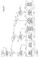
- FIG. 10 is a flowchart for explaining a process performed by the EC/KBC 120 in the first embodiment.
- the EC/KBC 120 waits until a detection voltage of the input terminal 110 rises from 0 [V], that is, a connection of the AC adapter 1 is detected (step S200).
- step S202 When the connection of the AC adapter 1 is detected, it is determined whether or not the suppliable current of the AC adapter 1 indicates "low”, based on the detected voltage of the input terminal 110 (step S202). When the suppliable current of the AC adapter 1 does not indicate “low”, it is determined whether the current indicates "medium”. Moreover, when the suppliable current of the AC adapter 1 does not indicate “medium”, it is determined whether the current indicates "high” (steps S210 and S218).
- step S204 it is determined whether the switch 172 is in the ON state, that is, it is determined whether the electronic apparatus 101 is in an operation.
- the switches 170 and 174 are turned on, and the battery 130 is charged by power supplied from the AC adapter 1 (step S206).
- the switch 170 is turned off and the power supplied from the AC adapter 1 is shut off, so that the electronic apparatus 101 successively operates by power from the battery 130 (step S208).
- step S212 it is determined whether the switch 172 is in the ON state, that is, the electronic apparatus 101 is in the operation.
- the switches 170 and 174 are turned on, and the battery 130 is charged by the power supplied from the AC adapter 1 (step S214).
- the switch 170 is turned on, the switches 174 and 176 are turned off to shut off the power supplied from the battery 130, and the electronic apparatus 101 is switched to the operation by the AC adapter 1 (step S216).
- step S220 When the suppliable current of the AC adapter 1 indicates "high", regardless of a state of the switch 172, the switches 170 and 174 are turned on and the switch 176 is also turned off (step S220). By this switching operation, it is possible to charge the battery 130 by power supplied from the adapter 1, and it is also for the electronic apparatus 101 to operate.
- step S222 it is determined whether the switch 172 is turned on, that is, the electronic apparatus 101 is in the operation.
- the switch 170 is turned off (step S224). In this case, any of charging the battery 130 and supplying power for the operation of the electronic apparatus 101 is not performed.
- the EC/KBC 120 displays a popup screen described later, and performs an exception process such as a state selection by a user (step S226).
- the OS When the OS of the electronic apparatus 101 receives the interruption, the OS displays, at the display 208, a message indicating that the interruption is made (the pop-up screen 8a in FIG. 4 ).
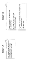
- FIG. 11A and FIG. 11B are diagrams illustrating examples of the popup screen displayed when the AC adapter 1 is connected.
- FIG. 11A illustrates a screen 11a displayed when the AC adapter 1 of "suppliable current - low" is connected to the electronic apparatus 101.
- FIG. 11B illustrates a screen 11b displayed when the AC adapter 1 of "suppliable current - unclear” is connected to the electronic apparatus 101.
- Information selection information in FIG. 4
- the EC/KBC 120 receives information from the OS, and operates the switches 170 through 176 based on an instruction from the OS. In this case, if no selection is made by the user in a certain time, the EC/KBC 120 may turn off the switch 170 and shut off the AC adapter 1.
- the AC adapter 1 in the first embodiment by setting the predetermined voltage Vh based on the specification of the AC adapter 1, it is possible to report the specification of the AC adapter 1 to the electronic apparatus 101 being the main device. Also, since the number of the output terminals is not increased to report the specification of the AC adapter 1, it is possible to suppress the increase of the expense and the size of the AC adapter.
- a proper state control is performed based on the specification of the AC adapter 1. Therefore, it is possible to prevent problems in which since the suppliable power of the AC adapter 1 becomes insufficient, the operation of the electronic apparatus 101 stops and the battery 130 is not sufficiently charged.
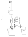
- FIG. 12 is a diagram for explaining an effect of the first embodiment.
- an AC adapter 1g corresponds to an application example of the AC adapter 1 of "suppliable current - high”
- the AC adapter Is corresponds to an application example of the AC adapter 1 of "suppliable current - low”.
- the electronic apparatus 101g corresponds to an application example of the electronic apparatus 101 having great power consumption
- the electronic apparatus 101s corresponds to the electronic apparatus 101 having a small power consumption.
- the AC adapter 1g is connected to the electronic apparatus 101g, it is possible to charge the battery 130 and supply power for the operation of the electronic apparatus 101g.
- the electronic apparatus 101g is connected to the AC adapter 1s, it is possible only to charge the battery 130.
- the AC adapter Is is connected to the electronic apparatus 101s, it is possible to charge the battery 130 and also supply the power for the operation of the electronic apparatus 101g. Accordingly, if the AC adapter 1 reports the specification of the AC adapter 1 itself to the electronic apparatus 101, it is possible to perform the state control depending on the specification of the AC adapter 1. Thus, it is possible to extend a variety of combinations of the AC adapter 1 and the electronic apparatus 101. That is, it is possible to improve compatibility of the AC adapter 1.
- the AC adapter 1 and the electronic apparatus 101 correspond to an example of an "electronic apparatus unit" in claims.
- FIG. 13 is a diagram illustrating a partial configuration in a state in which the AC adapter 2 is connected to the electronic apparatus 102 in the second embodiment.
- the AC adapter 2 includes the contact 10 as the input terminal, and the contact 20 as the output terminal, the transformer 30, the rectification-smoothing circuit 35, and a voltage adjustment circuit 50.
- Components other than the voltage adjustment circuit 50 are the same as those in the first embodiment, and the explanation thereof will be omitted.
- the voltage adjustment circuit 50 includes a resistor 52, and a Positive Thermal Constant (PTC) 54 as an overcurrent protecting fuse.
- the PTC 54 may be a device which has a positive temperature coefficient indicating that a resistance value increases depending on a temperature increase.
- the electronic apparatus 102 in the second embodiment includes a capacitor 114 parallel to a pull-down resistor 112, in addition to components which the electronic apparatus 101 in the first embodiment includes.
- FIG. 14 is a diagram illustrating changes of resistance values of the voltage adjustment circuit 50 from timing of connecting the AC adapter 2 to the electronic apparatus 102 in the second embodiment.
- a resistance value R1 of the resistor 52 a resistance value R2 of the PTC 54, and a combined resistance value R of combining the resistance values R1 and R2 are illustrated.
- the resistance value R1 is indicated by a thin solid line
- the resistance value R2 is indicated by a dashed line
- the combined resistance value R is indicated by a heavy line.
- a voltage decrease 14a from the resistance value R1 to the combined resistance value R being approximately 0 [ ⁇ ] is illustrated in FIG. 14 .
- the resistance value R2 When the resistance value R2 is sufficiently increased, the combined resistance value R becomes approximately the same as the resistance value R1, and current almost does not flow to the PTC 54. Moreover, when a charge of the capacitor 114 ends, the transient current Is does not flow. As a result, temperature of the PTC 54 decreases, and the resistance value R2 becomes nearly 0 [ ⁇ ].
- the resistance value R2 When the resistance value R2 is near 0 [ ⁇ ], the combined resistance value R is near 0 [ ⁇ ]. However, in this steady state, the transient current Is, which is a sharp current immediately after the AC adapter 2 is connected to the electronic apparatus 102, does not flow. The resistance value R2 is retained to be sufficiently lower than the resistance value R1, and a regular power supply is continued.
- the AC adapter 2 temporarily raises a resistance value by using heat of the PTC 54 due to the transient current Is generated immediately after the AC adapter 2 is connected to the electronic apparatus 102. Accordingly, a voltage of the contact 20 is decreased by a predetermined voltage Vh from a regular supply voltage Vn (which may be 19 [V]) by a temporary increase of the resistance value.
- the predetermined voltage Vh is almost determined based on the resistance value R1 of the resistor 52. Accordingly, by properly selecting the resistance value R1 of the resistor 52, it is possible to realize a predetermined voltage Vh which is desired.
- timing represented by "DETERMINATION” is set beforehand in the electronic apparatus 102 to be included in a term in which the combined resistance value R becomes the resistance value R1, based on an experiment or the like.
- the operation state is determined as one of three states:(1) only charging the battery 130, (2) only conducting an actual operation, and (3) charging the battery 130 and conducting the actual operation.
- the predetermined voltage Vh is set based on the specification of the AC adapter 2.
- the electronic apparatus 102 being the main device.
- the number of the output terminals is not increased, it is possible to suppress the increase of the cost and the size of the electronic apparatus 102.
- the electronic apparatus 102 in the second embodiment it is possible to conduct the proper state control based on the specification of the AC adapter 2. Therefore, it is possible to prevent problems in which the suppliable power of the AC adapter 1 becomes insufficient, the operation of the electronic apparatus 101 stops, and the battery 130 is not sufficiently charged.
- an effect in the second embodiment is the same as the effect described with reference to FIG. 12 in the first embodiment.
- it is possible to improve the compatibility of the AC adapter 2.
- the AC adapter 2 and the electronic apparatus 102 correspond to an example of the "electronic apparatus unit" in claims.
- the present invention may be used in production industries of an electronic apparatus typified by an electronic apparatus and an AC adapter being a peripheral device thereof.
Landscapes
- Engineering & Computer Science (AREA)
- Power Engineering (AREA)
- Charge And Discharge Circuits For Batteries Or The Like (AREA)
- Rectifiers (AREA)
- Dc-Dc Converters (AREA)
Abstract
Description
- The embodiments discussed herein are related to an AC adapter for converting an alternating current into a direct current and supplying the direct current to an electronic apparatus, and an electronic apparatus unit including the AC adapter and the electronic apparatus.
- Conventionally, an alternator such as a commercial power or the like supplied through a household outlet has been widely used. On the other hand, an electronic apparatus such as a computer or the like generally operates with the direct current. Accordingly, an AC adapter is used to convert an alternating current into a direct current and supply the direct current to an electronic apparatus (hereinafter, called "main device").
- The AC adapter has a different rated current, a different type, and the like depending on its size or the like. By these different features, power to be supplied becomes different. However, since it is not possible to determine the rated current, the different type, and the like of the AC adapter at a side of the main device, a relationship between the main device and the AC adapter has been fixed. Accordingly, there is no compatibility between models, or manufacturers, and the AC adapter has not been standardized between different models, or manufacturers.
- Also, in a state of supplying power from the AC adapter to the main device, in an order of a state of a smaller power consumption, the state of the power supply may be one of the following states: (1) a state of conducting power supply only to charge an internal battery of the main device, (2) a state of conducting power supply only for an actual operation of the main device. Moreover, as a state in which the power consumption is great, the power supply may be in (3) a state of conducting power supplies for a charge of the internal battery and for an actual operation of the main device. However, there is no guarantee that the AC adapter supports all states by its possible power to supply.
- Technologies related to the above described problems have been known as follows.
- Japanese Laid-open Patent Application No.
2004-341592 - Also, Japanese Laid-open Patent Application No.
H07-143749 - Moreover, Japanese Laid-open Patent Application No.
H05-184065 - Furthermore, Japanese Laid-open Patent Application No.
2000-134816 2000-134816 - However, in a system disclosed in Japanese Laid-open Patent Application No.
2004-341592 - Also, in the AC adapter disclosed in Japanese Laid-open Patent Application No.
H07-143749 - Moreover, in the AC adapter disclosed in Japanese Laid-open Patent Application No.
H05-184065 - Furthermore, in the system disclosed in Japanese Laid-open Patent Application No.
2000-134816 - In view of the above-mentioned conventional problems, the present disclosure aims at providing an AC adapter which improves compatibility, and an electronic apparatus unit using the AC adapter.
- According to one aspect of the embodiment, there is provided an AC adapter including a conversion part configured to convert alternating current input to an input terminal into a direct current; an output terminal configured to supply the direct current to an electronic apparatus outside; and a voltage adjusting circuit configured to lower a voltage of the output terminal by a predetermined voltage from a regular supply voltage in a term after the AC adapter is connected to the electronic apparatus until a predetermined time lapses.
-
-
FIG. 1 is an outline diagram illustrating a state in which an AC adapter according to a first embodiment; -
FIG. 2 is a diagram illustrating a circuit configuration of the AC adapter according to the first embodiment; -
FIG. 3 is a diagram illustrating a state change of each of components of the AC adapter in a term after the AC adapter is connected to an AC outlet and is mounted to an electronic apparatus and until power supply starts to the electronic apparatus; -
FIG. 4 is a diagram illustrating an example of a circuit configuration of the electronic apparatus; -
FIG. 5 is a diagram illustrating a circuit configuration example of a standing power supply circuit; -
FIG. 6 is a diagram illustrating a circuit configuration example of a charging circuit; -
FIG. 7 is a diagram illustrating a circuit configuration example of a power supply circuit; -
FIG. 8 is a diagram illustrating a mechanism for the electronic apparatus to determine a specification of the AC adapter; -
FIG. 9 is a diagram for illustrating a relationship between a predetermined voltage Vh and a suppliable current of the AC adapter; -
FIG. 10 is a flowchart for explaining a process performed by an EC/KBC; -
FIG. 11A and FIG. 11B are diagrams illustrating examples of a popup screen displayed when the AC adapter is connected; -
FIG. 12 is a diagram for explaining an effect of the first embodiment; -
FIG. 13 is a diagram illustrating a partial configuration in a state in which an AC adapter is connected to an electronic apparatus in a second embodiment; and -
FIG. 14 is a diagram illustrating changes of resistance values of a voltage adjustment circuit from timing of connecting the AC adapter to the electronic apparatus. - In the following, embodiments of the present invention will be described with reference to the accompanying drawings.
- An
AC adapter 1 and anelectronic apparatus 101 using an AC adapter will be described according to a first embodiment. -
FIG. 1 is an outline diagram illustrating a state in which theAC adapter 1 according to the first embodiment is connected to theelectronic apparatus 101. As illustrated inFIG. 1 , in the AC adapter 1 (or anAC adapter 2 described later in a second embodiment), onecontact 10 as a plug-in is connected to anAC outlet 10a for household use, and anothercontact 20 as a terminal is connected to aninput terminal 110 of theelectronic apparatus 101. Theelectronic apparatus 101 may be regarded as a laptop personal computer, and functions as the main device using theAC adapter electronic apparatus 101, a desktop personal computer, an Audio Visual (AV) device such as a television and a game machine, a portable television, and the like may be used. -
FIG. 2 is a diagram illustrating a circuit configuration of theAC adapter 1 according to the first embodiment. As illustrated inFIG. 2 , theAC adapter 1 includes thecontact 10 being an input terminal as the plug, thecontact 20 being an output terminal, atransformer 30, a rectification-smoothing circuit 35, and avoltage adjusting circuit 40. - The
transformer 30 may lower an alternating current input to thecontact 10 to AC 19/ (√2) [V]. The alternating current input to thecontact 10 may be regarded as power of AC 100 [V] for a commercial use. - The rectification-smoothing
circuit 35 includes adiode 36, acapacitor 37, and the like. The rectification-smoothingcircuit 35 converts the alternating current output from thetransformer 30 into the direct current, and outputs the direct current to a side of thevoltage adjusting circuit 40. A configuration of the rectification-smoothingcircuit 35 illustrated inFIG. 2 is an example. Another configuration including a bridge circuit or the like may be applied. - The
voltage adjusting circuit 40 may be formed by a time-limit operation circuit, and includes aresistors transistors capacitor 44. Thevoltage adjusting circuit 40 lowers a voltage of theconnector 20 in a predetermined time T1 after theAC adapter 1 is connected to theelectronic apparatus 101, from a regular supply voltage Vn (which may be 19 [V]) to a predetermined voltage Vh. - The
resistor 41A is regarded as an output impedance element for determining the predetermined voltage Vh. The predetermined voltage Vh represents an information value for sending information of the specification of theAC adapter 1 to a side of theelectronic apparatus 101. The information of the specification may indicate suppliable current, and may include information of an output voltage, a product number, a manufacturer, and the like. Details will be described later. - The P-
channel FET 42 changes from an OFF state to an ON state when the predetermined time T1 passes after theAC adapter 1 is connected to theelectronic apparatus 101. By this configuration, the current flows to thecontact 20 through the P-channel FET 42, a voltage in thecontact 20 rises to the regular supply voltage Vn. - Other configuration parts of the
voltage adjusting circuit 40 are used for theresistor 41A and the P-channel FET 42 described above to operate. In the following, a state change of each of components of theAC adapter 1 will be described.FIG. 3 is a diagram illustrating the state change of each of the components of theAC adapter 1 in a term after theAC adapter 1 is connected to theAC outlet 10a and is mounted to theelectronic apparatus 101 and until power supply starts to theelectronic apparatus 101. - As illustrated in
FIG. 3 , when theAC adapter 1 is connected to theAC outlet 10a (time t1), the voltage in thecontact 20 rises to the regular supply voltage Vn. After that, when thecontact 20 is connected to the electronic apparatus 101 (time t2), the current flows from theAC adapter 1 to theelectronic apparatus 101, and a state of thetransistor 43A changes from the OFF state to the ON state in response to a voltage drop. When thetransistor 43A is in the ON state, the current, which is determined based on resistance values of theresistors capacitor 44, and thecapacitor 44 is charged. - Accordingly, the predetermined time T1 passes from the time t2. When a charging voltage of the
capacitor 44 becomes higher than a certain voltage Vbe (time t3), thetransistor 43C changes from the OFF state to the ON state, and lowers a gate voltage of the P-channel FET 42 to 0 [V]. As a result, the P-channel FET 42 changes from the OFF state to the ON state, and the voltage of thecontact 20 rises to the regular supply voltage Vn. - When the state of
transistor 43C becomes the ON state, the state of thetransistor 43B becomes the ON state, and a base current of thetransistor 43C is supplied. Accordingly, thetransistor 43C is retained in the ON state. - As described above, when the
contact 20 is connected to theelectronic apparatus 101, thecapacitor 44 is charged. When the charging voltage becomes a certain voltage Vbe after a certain time lapses, thetransistor 43C is retained in the ON state. As a result, the voltage of thecontact 20 rises to the regular supply voltage Vn, and the power supply starts to theelectronic apparatus 101. - According to the above described configurations, by appropriately selecting the resistance value of the
resistor 41A, it is possible to realize the predetermined voltage Vh. By selecting the predetermined voltage Vh based on the specification of theAC adapter 1, it is possible to send the information of the specification of theAC adapter 1 to theelectronic apparatus 101. Also, the number of terminals is not increased to send the information of the specification. It is possible to suppress increasing the expense and the size of theAC adapter 1. -
FIG. 4 is a diagram illustrating an example of a circuit configuration of theelectronic apparatus 101. As illustrated inFIG. 4 , theelectronic apparatus 101 includes theinput terminal 110, a pull-down resistor 112, an EC (Enabled Controller)/KBC (Keyboard Controller) 120, abattery 130, a standingpower supply circuit 140, a chargingcircuit 150, and apower supply circuit 160.Switches - The EC/
KBC 120 internally mounts a Central Processing Unit (CPU) and an A/D convertor 120A, and controls a pointing device such as a keyboard (KB), a mouse, and the like. Also, the EC/KBC 120 conducts various processes using its processing ability, and is operated by the power supply from the standingpower supply circuit 140 which is an independent power supply circuit. -
FIG. 5 is a diagram illustrating a circuit configuration example of the standingpower supply circuit 140. The standingpower supply circuit 140 operates as a power supply circuit which outputs a lower current always being supplied. The standingpower supply circuit 140 may be a dropper type circuit in which an input voltage Vin is input from thebattery 130 and a 3.3 [V] voltage is output. The standingpower supply circuit 140 includes atransistor 142 retaining the base voltage at 4 [V] by a Zener diode 141, acapacitor 143, avoltage drop resistor 144, and the like. -
FIG. 6 is a diagram illustrating a circuit configuration example of the chargingcircuit 150. The chargingcircuit 150 may utilize a circuit of CC (Constant Current) / CV (Constant Voltage) method, and may include a constantcurrent charging circuit 151, a constantvoltage charging circuit 152, a chargingvoltage detection circuit 153, and an endingcurrent detection circuit 154. - The constant
current charging circuit 151 includes aZener diode 151A,transistors resistors Zener diode 151A, thetransistor 151B, and theresister 151D are connected in parallel to theZener diode 151A. A base of thetransistor 151B is connected to an output terminal of the chargingvoltage detection circuit 153 through theresistor 151G. An emitter of thetransistor 151B is connected to the input voltage Vin, and a collector of thetransistor 151B is connected to an anode side of theZener diode 151A through theresistor 151E. Also, a base of thetransistor 151C is connected to a collector of thetransistor 151B. An emitter of thetransistor 151C is connected to the input voltage Vin through theresistor 151D, and the collector of thetransistor 151C is connected to the output terminal of the charging voltage. - The constant
voltage charging circuit 152 includes aZener diode 152A, atransistor 152B, andresistors Zener diode 152A is connected to the input voltage Vin through theresistor 152C, and is also connected to a base of thetransistor 152B through theresistor 152D. A collector of thetransistor 152B is connected to the input voltage Vin. An emitter of thetransistor 152B is connected to a negative terminal of anoperational amplifier 154B of the endingcurrent detection circuit 154, and is also connected to an output terminal of the charging voltage through theresistor 152E. - The charging
voltage detection circuit 153 includes adiode 153A, anoperational amplifier 153B, aninverter 153C, and aresistor 153D. An anode side of thediode 153A is connected to an output terminal of the endingcurrent detection circuit 154. A cathode side of thediode 153A is connected to the input voltage Vin through theresistor 153D, and is also connected to an output terminal of theoperational amplifier 153B and an input side of theinverter 153C. A positive terminal of theoperational amplifier 153B is connected to the input voltage Vin through theresistor 152C, and the charging voltage is negatively fed back to a negative terminal of theoperational amplifier 153B. - The ending
current detection circuit 154 includes a constantcurrent generator 154A, anoperational amplifier 154B, and aresistor 154C. The input voltage Vin is input to the constantcurrent generator 154A. An output terminal of the constantcurrent generator 154A is connected to a positive terminal of theoperational amplifier 154B, and is also connected to an output terminal of the charging voltage through theresistor 154C. - The charging
circuit 150 conducts charging with the same charging voltage as a rated output current at a first stage. When the voltage of the battery achieves a rated voltage, a charge with a constant voltage is performed at a second stage. Accordingly, when a charging current becomes equal to or lower than a certain voltage, the chargingcircuit 150 ends charging thebattery 130. In thecharging circuit 150 in the first embodiment, it is assumed that thebattery 130 as a charging target is a lithium ion secondary battery of fourth DC 14.4 [V] and 2200 [mAH]. -
FIG. 7 is a diagram illustrating a circuit configuration example of thepower supply circuit 160. Thepower supply circuit 160 may include a Pulse Width Modulation (PWM)circuit 161, a Metal Oxide Semiconductor (P-MOS) 162, an N-MOS 163, acoils capacitors power supply circuit 160 may be a power supply circuit of a PWM method and a synchronous rectifying type. Thepower supply circuit 160 supplies basic power inside itself. - Also, the
electronic apparatus 101 includes a Platform Controller Hub (PCH) 200, a Central Processing Unit (CPU) 202, a Read-Only Memory (ROM) 204, and memory (MEM) 206. Moreover, theelectronic apparatus 101 includes adisplay 208, a Hard Disk Drive (HDD) 210, a keyboard/mouse 212, and the like. - The
PCH 200 is generally called a chipset, and functions as an interface to a peripheral device. TheCPU 202 is regarded as a processor including a calculation process function and a memory control function. TheROM 204 may be a non-volatile memory used to load an Operating System (OS) from aHard Disk Drive 210, and to store a Basic Input Output System (BIOS) being a program to start up a system. TheMEM 206 is connected to an EEPROM (Electrically Erasable and Programmable Read Only Memory) and theCPU 202, and stores the OS, an application program, and data. Thedisplay 208 displays a human/machine interface. TheHDD 210 stores the OS, the application programs, and the data as an auxiliary storage device. - In the following, a specification determination of the
AC adapter 1 performed by theelectronic apparatus 101 in the first embodiment will be described.FIG. 8 is a diagram illustrating a mechanism for theelectronic apparatus 101 to determine the specification of theAC adapter 1 in the first embodiment. When theAC adapter 1 is connected theelectronic apparatus 101, thecontact 20 is connected to theinput terminal 110. Then, anoutput impedance 41A of theAC adapter 1, and a voltage across the pull-down resistor 112, which is divided by the pull-down resistor 112 at a side of theelectronic apparatus 101, are input into the A/D convertor 120A of the EC/KBC 120. It should be noted that if thecontact 20 is not connected to theinput terminal 110, a detected voltage of theinput terminal 110 becomes a ground level (0 [V]). - The EC/
KBC 120 monitors a voltage generated from the pull-down resistor 112 by current flowing in the pull-down resistor 112 in a predetermined time after theAC adapter 1 is connected, and determines the specification of theAC adapter 1 by the generated voltage. - As described above, the
AC adapter 1 lowers a voltage in thecontact 20 by a predetermined voltage Vh from the regular supply voltage Vn in the predetermined time after theAC adapter 1 is connected. If the current of theAC adapter 1 possible to supply is classified into three stages: a high stage, a medium stage, and a low stage, by the specification, the predetermined voltage Vh may be determined as follows: - suppliable current - high:
- in a range of Vh = Vn× (9/12) to Vn× (11/12) suppliable current - medium :
- in a range of Vh = Vn× (4/12) to Vn× (7/12) suppliable current - low :
- in a range of Vh = Vn× (1/12) to Vn× (3/12)
-
FIG. 9 is a diagram for illustrating a relationship between the predetermined voltage Vh and the suppliable current of theAC adapter 1. As illustrated inFIG. 9 , a range of Vh = Vn× (11/12) to Vn, a range of Vh = Vn× (7/12) to Vn× (8/12), and a range of Vh = 0 to Vn× (1/12) are unclear zones in the specification of the AC adapter 1 (represented byguard bands 9a inFIG. 8 ). By using the above described ranges, it is possible to suppress an improper operation of theelectronic apparatus 101 due to a measurement error. The entire range may be used as a main determination condition, and a sub-determination condition may be set in each of the above described ranges. - As described above, the specification of the
AC adapter 1, which is determined by the EC/KBC 120, may not be limited to the suppliable current. The specification may indicate the output voltage, a product number, a manufacturer, or the like. - Accordingly, it is possible for the
AC adapter 1 to detect theelectronic apparatus 101. As a result, a proper control described below is performed. - In the following, an operation control of the
electronic apparatus 101, which depends on the specification of theAC adapter 1 and is determined by the EC/KBC 120, will be described. Based on the specification of theAC adapter 1, theelectronic apparatus 101 determines one of operational states of: (1) only charging thebattery 130, (2) only conducting an actual operation, and (3) charging thebattery 130 and conducting the actual operation. A state of conducting the "actual operation" may be a state of a regular operation other than charging thebattery 130 is conducted. -
FIG. 10 is a flowchart for explaining a process performed by the EC/KBC 120 in the first embodiment. - First, the EC/
KBC 120 waits until a detection voltage of theinput terminal 110 rises from 0 [V], that is, a connection of theAC adapter 1 is detected (step S200). - When the connection of the
AC adapter 1 is detected, it is determined whether or not the suppliable current of theAC adapter 1 indicates "low", based on the detected voltage of the input terminal 110 (step S202). When the suppliable current of theAC adapter 1 does not indicate "low", it is determined whether the current indicates "medium". Moreover, when the suppliable current of theAC adapter 1 does not indicate "medium", it is determined whether the current indicates "high" (steps S210 and S218). - When the suppliable current of the
AC adapter 1 indicates "low", it is determined whether theswitch 172 is in the ON state, that is, it is determined whether theelectronic apparatus 101 is in an operation (step S204). When theelectronic apparatus 101 is not in the operation, theswitches battery 130 is charged by power supplied from the AC adapter 1 (step S206). On the other hand, when theelectronic apparatus 101 is in the operation, theswitch 170 is turned off and the power supplied from theAC adapter 1 is shut off, so that theelectronic apparatus 101 successively operates by power from the battery 130 (step S208). - When the suppliable current of the
AC adapter 1 indicates "medium", it is determined whether theswitch 172 is in the ON state, that is, theelectronic apparatus 101 is in the operation (step S212). When theelectronic apparatus 101 is not in the operation, theswitches battery 130 is charged by the power supplied from the AC adapter 1 (step S214). On the other hand, when theelectronic apparatus 101 is in the operation, theswitch 170 is turned on, theswitches battery 130, and theelectronic apparatus 101 is switched to the operation by the AC adapter 1 (step S216). - When the suppliable current of the
AC adapter 1 indicates "high", regardless of a state of theswitch 172, theswitches switch 176 is also turned off (step S220). By this switching operation, it is possible to charge thebattery 130 by power supplied from theadapter 1, and it is also for theelectronic apparatus 101 to operate. - When the suppliable current of the
AC adapter 1 is not any of "low", "medium", and "high" and is unclear, it is determined whether theswitch 172 is turned on, that is, theelectronic apparatus 101 is in the operation (step S222). When theelectronic apparatus 101 is in the operation, theswitch 170 is turned off (step S224). In this case, any of charging thebattery 130 and supplying power for the operation of theelectronic apparatus 101 is not performed. On the other hand, in a case in which theelectronic apparatus 101 is in the operation, the EC/KBC 120 displays a popup screen described later, and performs an exception process such as a state selection by a user (step S226). - According to the above described process, it is possible to conduct a proper state control depending on the specification of the
AC adapter 1. By this process, it is possible to prevent problems in which the suppliable power of theAC adapter 1 becomes insufficient, the operation of theelectronic apparatus 101 stops, and thebattery 130 is not sufficiently charged. Accordingly, it is possible for theelectronic apparatus 101 to allow for theAC adapter 1 which is minimized with light weight and is used only to charge the power. Then, it is possible to expand a product lineup. - In the following, a screen display process in a case for the
electronic apparatus 101 to detect the connection of theAC adapter 1 will be described. In a case in which the connection of theAC adapter 1 is detected, if the OS of theelectronic apparatus 101 is activated, the EC/KBC 120 generates an interruption and sends a determination result of the AC adapter 1 (detection information inFIG. 4 ). - When the OS of the
electronic apparatus 101 receives the interruption, the OS displays, at thedisplay 208, a message indicating that the interruption is made (the pop-upscreen 8a inFIG. 4 ). -
FIG. 11A and FIG. 11B are diagrams illustrating examples of the popup screen displayed when theAC adapter 1 is connected.FIG. 11A illustrates ascreen 11a displayed when theAC adapter 1 of "suppliable current - low" is connected to theelectronic apparatus 101.FIG. 11B illustrates ascreen 11b displayed when theAC adapter 1 of "suppliable current - unclear" is connected to theelectronic apparatus 101. By displaying thescreen 11b, the user is urged to select a radio button. Information (selection information inFIG. 4 ) selected by the user is sent to the EC/KBC 120. The EC/KBC 120 receives information from the OS, and operates theswitches 170 through 176 based on an instruction from the OS. In this case, if no selection is made by the user in a certain time, the EC/KBC 120 may turn off theswitch 170 and shut off theAC adapter 1. - According to the
AC adapter 1 in the first embodiment, by setting the predetermined voltage Vh based on the specification of theAC adapter 1, it is possible to report the specification of theAC adapter 1 to theelectronic apparatus 101 being the main device. Also, since the number of the output terminals is not increased to report the specification of theAC adapter 1, it is possible to suppress the increase of the expense and the size of the AC adapter. - According to the
electronic apparatus 101 in the first embodiment, a proper state control is performed based on the specification of theAC adapter 1. Therefore, it is possible to prevent problems in which since the suppliable power of theAC adapter 1 becomes insufficient, the operation of theelectronic apparatus 101 stops and thebattery 130 is not sufficiently charged. -
FIG. 12 is a diagram for explaining an effect of the first embodiment. InFIG. 12 , anAC adapter 1g corresponds to an application example of theAC adapter 1 of "suppliable current - high", and the AC adapter Is corresponds to an application example of theAC adapter 1 of "suppliable current - low". Also, theelectronic apparatus 101g corresponds to an application example of theelectronic apparatus 101 having great power consumption, and theelectronic apparatus 101s corresponds to theelectronic apparatus 101 having a small power consumption. In this configuration, in a case in which theAC adapter 1g is connected to theelectronic apparatus 101g, it is possible to charge thebattery 130 and supply power for the operation of theelectronic apparatus 101g. On the other hand, in a case in which theelectronic apparatus 101g is connected to theAC adapter 1s, it is possible only to charge thebattery 130. In a case in which the AC adapter Is is connected to theelectronic apparatus 101s, it is possible to charge thebattery 130 and also supply the power for the operation of theelectronic apparatus 101g. Accordingly, if theAC adapter 1 reports the specification of theAC adapter 1 itself to theelectronic apparatus 101, it is possible to perform the state control depending on the specification of theAC adapter 1. Thus, it is possible to extend a variety of combinations of theAC adapter 1 and theelectronic apparatus 101. That is, it is possible to improve compatibility of theAC adapter 1. - In the first embodiment, the
AC adapter 1 and theelectronic apparatus 101 correspond to an example of an "electronic apparatus unit" in claims. - In the following, an
AC adapter 2 and anelectronic apparatus 102 using theAC adapter 2 in a second embodiment will be described. -
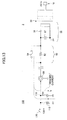
FIG. 13 is a diagram illustrating a partial configuration in a state in which theAC adapter 2 is connected to theelectronic apparatus 102 in the second embodiment. As illustrated inFIG. 13 , theAC adapter 2 includes thecontact 10 as the input terminal, and thecontact 20 as the output terminal, thetransformer 30, the rectification-smoothingcircuit 35, and avoltage adjustment circuit 50. Components other than thevoltage adjustment circuit 50 are the same as those in the first embodiment, and the explanation thereof will be omitted. - In the second embodiment, the
voltage adjustment circuit 50 includes aresistor 52, and a Positive Thermal Constant (PTC) 54 as an overcurrent protecting fuse. ThePTC 54 may be a device which has a positive temperature coefficient indicating that a resistance value increases depending on a temperature increase. - Moreover, the
electronic apparatus 102 in the second embodiment includes acapacitor 114 parallel to a pull-down resistor 112, in addition to components which theelectronic apparatus 101 in the first embodiment includes. -
FIG. 14 is a diagram illustrating changes of resistance values of thevoltage adjustment circuit 50 from timing of connecting theAC adapter 2 to theelectronic apparatus 102 in the second embodiment. InFIG. 14 , a resistance value R1 of theresistor 52, a resistance value R2 of thePTC 54, and a combined resistance value R of combining the resistance values R1 and R2 are illustrated. The resistance value R1 is indicated by a thin solid line, the resistance value R2 is indicated by a dashed line, and the combined resistance value R is indicated by a heavy line. Avoltage decrease 14a from the resistance value R1 to the combined resistance value R being approximately 0 [Ω] is illustrated inFIG. 14 . - When the
AC adapter 2 is connected to theelectronic apparatus 102 in a state in which AC 100 [V] has been supplied to theAC adapter 2, a sharp transient current illustrated by Is inFIG. 13 flows toward thecapacitor 114. Due to the transient current Is, thePTC 54 is heated, and the resistance value R2 is increased. - When the resistance value R2 is sufficiently increased, the combined resistance value R becomes approximately the same as the resistance value R1, and current almost does not flow to the
PTC 54. Moreover, when a charge of thecapacitor 114 ends, the transient current Is does not flow. As a result, temperature of thePTC 54 decreases, and the resistance value R2 becomes nearly 0 [Ω]. - When the resistance value R2 is near 0 [Ω], the combined resistance value R is near 0 [Ω]. However, in this steady state, the transient current Is, which is a sharp current immediately after the
AC adapter 2 is connected to theelectronic apparatus 102, does not flow. The resistance value R2 is retained to be sufficiently lower than the resistance value R1, and a regular power supply is continued. - In the second embodiment, the
AC adapter 2 temporarily raises a resistance value by using heat of thePTC 54 due to the transient current Is generated immediately after theAC adapter 2 is connected to theelectronic apparatus 102. Accordingly, a voltage of thecontact 20 is decreased by a predetermined voltage Vh from a regular supply voltage Vn (which may be 19 [V]) by a temporary increase of the resistance value. The predetermined voltage Vh is almost determined based on the resistance value R1 of theresistor 52. Accordingly, by properly selecting the resistance value R1 of theresistor 52, it is possible to realize a predetermined voltage Vh which is desired. - In
FIG. 14 , timing represented by "DETERMINATION" is set beforehand in theelectronic apparatus 102 to be included in a term in which the combined resistance value R becomes the resistance value R1, based on an experiment or the like. - At the
electronic apparatus 102, contents of {Configuration}, {Specification Determination of AC Adapter}, {State Control}, {Screen Display Process}, {Screen Display Process}, and the like related to components other than thecapacitor 114 are the same as those in the first embodiment. In the second embodiment, similar to the first embodiment, based on the specification of theAC adapter 2, the operation state is determined as one of three states:(1) only charging thebattery 130, (2) only conducting an actual operation, and (3) charging thebattery 130 and conducting the actual operation. - According to the
AC adapter 2 in the second embodiment described above, the predetermined voltage Vh is set based on the specification of theAC adapter 2. Thus, it is possible to report the specification of theAC adapter 2 to theelectronic apparatus 102 being the main device. Moreover, since the number of the output terminals is not increased, it is possible to suppress the increase of the cost and the size of theelectronic apparatus 102. - Moreover, according to the
electronic apparatus 102 in the second embodiment, it is possible to conduct the proper state control based on the specification of theAC adapter 2. Therefore, it is possible to prevent problems in which the suppliable power of theAC adapter 1 becomes insufficient, the operation of theelectronic apparatus 101 stops, and thebattery 130 is not sufficiently charged. - Furthermore, an effect in the second embodiment is the same as the effect described with reference to
FIG. 12 in the first embodiment. Thus, it is possible to improve the compatibility of theAC adapter 2. - In the second embodiment, the
AC adapter 2 and theelectronic apparatus 102 correspond to an example of the "electronic apparatus unit" in claims. - The present invention may be used in production industries of an electronic apparatus typified by an electronic apparatus and an AC adapter being a peripheral device thereof.
- Accordingly, it is possible to provide the AC adapter in which the compatibility is improved and the electronic apparatus unit using the AC adapter.
- All examples and conditional language recited herein are intended for pedagogical purposes to aid the reader in understanding the invention and the concepts contributed by the inventor to furthering the art, and are to be construed as being without limitation to such specifically recited examples and conditions, nor does the organization of such examples in the specification relate to a showing of the superiority and inferiority of the invention. Although the embodiments of the present invention have been described in detail, it should be understood that the various changes, substitutions, and alterations could be made hereto without departing from the spirit and scope of the invention.
Claims (8)
- An AC adapter comprising:a conversion part configured to convert alternating current input to an input terminal into a direct current;an output terminal configured to supply the direct current to an electronic apparatus outside; anda voltage adjusting circuit configured to lower a voltage of the output terminal by a predetermined voltage from a regular supply voltage in a term after the AC adapter is connected to the electronic apparatus until a predetermined time lapses.
- The AC adapter as claimed in claim 1, wherein the predetermined voltage indicates a specification of the AC adapter.
- The AC adapter as claimed in claim 1 or 2, wherein the voltage adjusting circuit is formed by a time-limit operation circuit which increases or decreases a resistance voltage by switching a state of a semiconductor switch depending on a charge voltage change of a capacitor.
- The AC adapter as claimed in claim 1 or 2, wherein the voltage adjusting circuit includes a circuit in which an overcurrent protecting fuse and a resistor are connected in parallel to the output terminal.
- An electronic apparatus unit comprising:an AC adapter; andan electronic apparatus,wherein the AC adapter includes:a conversion part configured to convert alternating current input to an input terminal into a direct current;an output terminal configured to supply the direct current to an electronic apparatus outside; anda voltage adjusting circuit configured to lower a voltage of the output terminal by a predetermined voltage from a regular supply voltage in a term after the AC adapter is connected to the electronic apparatus until a predetermined time lapses,the electronic apparatus is configured to receive power supply by being connected to an output terminal of the AC adapter, and to include a control part configured to determine a specification of the AC adapter based on a voltage decrease amount when the output terminal of the AC adapter is connected.
- The electronic apparatus unit as claimed in claim 5, wherein the control part selects one of a state of charging an internal battery of the electronic apparatus, a state of performing an actual operation of the electronic apparatus, and a state of charging the internal battery and performing the actual operation of the electronic apparatus based on the specification of the AC adapter determined by the control part, to be a state of the electronic apparatus.
- An electronic apparatus which receives a power supply by being connected to an output terminal of an AC adapter, the electronic apparatus comprising:a control part configured to determine a specification of the AC adapter based on a voltage decrease amount of an output terminal of the AC adapter when the output terminal of the AC adapter is connected.
- The electronic apparatus as claimed in claim 7, wherein the control part selects one of a state of charging an internal battery of the electronic apparatus, a state of performing an actual operation of the electronic apparatus, and a state of charging the internal battery and performing the actual operation of the electronic apparatus based on the specification of the AC adapter determined by the control part, to be a state of the electronic apparatus.
Applications Claiming Priority (1)
| Application Number | Priority Date | Filing Date | Title |
|---|---|---|---|
| JP2011086747A JP5803228B2 (en) | 2011-04-08 | 2011-04-08 | AC adapter, electronic device unit |
Publications (3)
| Publication Number | Publication Date |
|---|---|
| EP2528190A2 true EP2528190A2 (en) | 2012-11-28 |
| EP2528190A3 EP2528190A3 (en) | 2015-02-25 |
| EP2528190B1 EP2528190B1 (en) | 2016-04-20 |
Family
ID=46149129
Family Applications (1)
| Application Number | Title | Priority Date | Filing Date |
|---|---|---|---|
| EP12162004.1A Not-in-force EP2528190B1 (en) | 2011-04-08 | 2012-03-29 | Ac adapter and electronic apparatus unit |
Country Status (4)
| Country | Link |
|---|---|
| US (1) | US9240734B2 (en) |
| EP (1) | EP2528190B1 (en) |
| JP (1) | JP5803228B2 (en) |
| CN (1) | CN102739081B (en) |
Families Citing this family (5)
| Publication number | Priority date | Publication date | Assignee | Title |
|---|---|---|---|---|
| TWI548178B (en) * | 2012-02-24 | 2016-09-01 | 緯創資通股份有限公司 | Charging device and charging method |
| TWI513168B (en) * | 2012-12-20 | 2015-12-11 | Compal Electronics Inc | Power conversion apparatus |
| US9112416B2 (en) * | 2012-12-20 | 2015-08-18 | Intel Corporation | AC adapter for electronic device |
| US10278044B2 (en) * | 2014-08-08 | 2019-04-30 | Intel IP Corporation | Systems and methods for transmitting and managing communication on dedicated short-range communication channels |
| EP3270483B1 (en) * | 2016-07-12 | 2022-06-29 | Nxp B.V. | Apparatus and associated method for battery charging |
Citations (4)
| Publication number | Priority date | Publication date | Assignee | Title |
|---|---|---|---|---|
| JPS5184065A (en) | 1975-01-21 | 1976-07-23 | Kikunami Koiru Kk | |
| JPH07143749A (en) | 1993-11-12 | 1995-06-02 | Canon Inc | AC adapter and equipment using AC adapter |
| JP2000134816A (en) | 1998-10-27 | 2000-05-12 | Toshiba Corp | Electronic equipment and AC adapter |
| JP2004341592A (en) | 2003-05-13 | 2004-12-02 | Nagano Japan Radio Co | Electronic equipment system |
Family Cites Families (18)
| Publication number | Priority date | Publication date | Assignee | Title |
|---|---|---|---|---|
| JP2776105B2 (en) | 1992-01-07 | 1998-07-16 | 三菱電機株式会社 | Electronic device and method for supplying power to electronic device |
| US5847543A (en) * | 1997-06-30 | 1998-12-08 | Compaq Computer Corporation | AC adapter with automatically optimized output voltage and power |
| JP2001224131A (en) * | 2000-02-08 | 2001-08-17 | Nec Yonezawa Ltd | Ac adaptor, information processor, method and apparatus for control of battery charging |
| EP1280249B1 (en) * | 2001-07-27 | 2019-03-13 | General Electric Technology GmbH | Protection and monitoring device for a generator and application of such a device |
| JP3772345B2 (en) * | 2002-01-22 | 2006-05-10 | セイコーエプソン株式会社 | Electronic equipment and power circuit |
| JP3799294B2 (en) * | 2002-05-15 | 2006-07-19 | ソニー株式会社 | Charger |
| JP3887750B2 (en) * | 2002-09-05 | 2007-02-28 | 富士通アクセス株式会社 | Inrush current prevention circuit |
| JP4085864B2 (en) * | 2003-03-28 | 2008-05-14 | 株式会社村田製作所 | Inrush current suppression circuit |
| JP4066189B2 (en) * | 2003-07-09 | 2008-03-26 | ミツミ電機株式会社 | AC adapter and charging method thereof |
| CN1578052B (en) * | 2003-07-09 | 2010-04-28 | 三美电机株式会社 | AC adapter and its charging method |
| JP3833649B2 (en) * | 2003-11-28 | 2006-10-18 | ローム株式会社 | Charging device and portable electronic device including the same |
| KR100582772B1 (en) * | 2004-03-18 | 2006-05-22 | (주)에스피에스 | Universal power supply |
| US7424626B2 (en) * | 2004-04-28 | 2008-09-09 | Hewlett-Packard Development Company, L.P. | Laptop computer recharging using Ethernet connection |
| US7581130B2 (en) * | 2004-11-12 | 2009-08-25 | Hewlett-Packard Development Company, L.P. | Power management system and method |
| JP2006271086A (en) * | 2005-03-23 | 2006-10-05 | Nec Electronics Corp | Charger |
| JP3849141B2 (en) * | 2005-05-31 | 2006-11-22 | 富士写真フイルム株式会社 | Power supply for portable equipment |
| WO2007143610A2 (en) * | 2006-06-05 | 2007-12-13 | Aurisma, Llc | Device for converting ac power to multiple dc outputs with retractable cords and multiple adapter tips |
| US20080258674A1 (en) * | 2007-04-23 | 2008-10-23 | David Hui | Quickly charging power supply apparatus |
-
2011
- 2011-04-08 JP JP2011086747A patent/JP5803228B2/en not_active Expired - Fee Related
-
2012
- 2012-02-29 CN CN201210050419.9A patent/CN102739081B/en not_active Expired - Fee Related
- 2012-03-29 EP EP12162004.1A patent/EP2528190B1/en not_active Not-in-force
- 2012-04-02 US US13/437,473 patent/US9240734B2/en not_active Expired - Fee Related
Patent Citations (4)
| Publication number | Priority date | Publication date | Assignee | Title |
|---|---|---|---|---|
| JPS5184065A (en) | 1975-01-21 | 1976-07-23 | Kikunami Koiru Kk | |
| JPH07143749A (en) | 1993-11-12 | 1995-06-02 | Canon Inc | AC adapter and equipment using AC adapter |
| JP2000134816A (en) | 1998-10-27 | 2000-05-12 | Toshiba Corp | Electronic equipment and AC adapter |
| JP2004341592A (en) | 2003-05-13 | 2004-12-02 | Nagano Japan Radio Co | Electronic equipment system |
Also Published As
| Publication number | Publication date |
|---|---|
| JP5803228B2 (en) | 2015-11-04 |
| US9240734B2 (en) | 2016-01-19 |
| US20120256597A1 (en) | 2012-10-11 |
| JP2012222971A (en) | 2012-11-12 |
| EP2528190A3 (en) | 2015-02-25 |
| EP2528190B1 (en) | 2016-04-20 |
| CN102739081A (en) | 2012-10-17 |
| CN102739081B (en) | 2015-04-22 |
Similar Documents
| Publication | Publication Date | Title |
|---|---|---|
| EP2528190B1 (en) | Ac adapter and electronic apparatus unit | |
| CN103718618B (en) | Monitor the battery in portable electric appts | |
| JP5652802B2 (en) | Internal short circuit detection device and internal short circuit detection method for secondary battery | |
| US7932636B2 (en) | Automatic start-up circuit and uninterruptible power supply apparatus having such automatic start-up circuit | |
| EP2365605A2 (en) | Charging apparatus, program | |
| CN109256825B (en) | Charging method and electronic device | |
| JPWO2009072281A1 (en) | Power management circuit | |
| WO2016043099A1 (en) | Charging device | |
| CN105004928B (en) | Method for measuring at least one resistance parameter and electronic device | |
| CN104838557A (en) | Apparatus and method for discharging a battery and determining a condition of the battery | |
| US20220037898A1 (en) | Controller, electricity storage system, and recording medium | |
| JPWO2014051084A1 (en) | Charger | |
| KR101957245B1 (en) | Electronic apparatus and method for drive control thereof | |
| US12388342B2 (en) | Electronic apparatus, display device, and voltage management method | |
| WO2018070306A1 (en) | Power supply control circuit, electronic device, and power supply control method | |
| US7345451B2 (en) | Power supply device | |
| WO2020042715A1 (en) | Electronic device power supply method and apparatus, electronic device, and storage medium | |
| US6339264B1 (en) | Apparatus and method for forecasting output voltage of a battery of a digital camera | |
| JP2006109618A (en) | Charge control circuit | |
| CN108333515B (en) | Uninterruptible power system that can display battery internal resistance information | |
| TW201937826A (en) | Charging device, method for determining charging sequence and method for power detection | |
| US20240088688A1 (en) | Storage battery management device, storage battery management method, and recording medium | |
| EP3663051B1 (en) | Battery unit and electric tool system | |
| JP5515337B2 (en) | Battery pack and information processing apparatus | |
| JP2015100220A (en) | Multiple battery power supply |
Legal Events
| Date | Code | Title | Description |
|---|---|---|---|
| PUAI | Public reference made under article 153(3) epc to a published international application that has entered the european phase |
Free format text: ORIGINAL CODE: 0009012 |
|
| AK | Designated contracting states |
Kind code of ref document: A2 Designated state(s): AL AT BE BG CH CY CZ DE DK EE ES FI FR GB GR HR HU IE IS IT LI LT LU LV MC MK MT NL NO PL PT RO RS SE SI SK SM TR |
|
| AX | Request for extension of the european patent |
Extension state: BA ME |
|
| PUAL | Search report despatched |
Free format text: ORIGINAL CODE: 0009013 |
|
| AK | Designated contracting states |
Kind code of ref document: A3 Designated state(s): AL AT BE BG CH CY CZ DE DK EE ES FI FR GB GR HR HU IE IS IT LI LT LU LV MC MK MT NL NO PL PT RO RS SE SI SK SM TR |
|
| AX | Request for extension of the european patent |
Extension state: BA ME |
|
| RIC1 | Information provided on ipc code assigned before grant |
Ipc: H02J 7/00 20060101ALI20150119BHEP Ipc: H02M 1/36 20070101ALI20150119BHEP Ipc: G01R 19/165 20060101ALI20150119BHEP Ipc: H02J 7/02 20060101AFI20150119BHEP Ipc: H02J 7/04 20060101ALI20150119BHEP Ipc: H02M 7/12 20060101ALI20150119BHEP |
|
| 17P | Request for examination filed |
Effective date: 20150709 |
|
| RBV | Designated contracting states (corrected) |
Designated state(s): AL AT BE BG CH CY CZ DE DK EE ES FI FR GB GR HR HU IE IS IT LI LT LU LV MC MK MT NL NO PL PT RO RS SE SI SK SM TR |
|
| GRAP | Despatch of communication of intention to grant a patent |
Free format text: ORIGINAL CODE: EPIDOSNIGR1 |
|
| INTG | Intention to grant announced |
Effective date: 20151023 |
|
| GRAS | Grant fee paid |
Free format text: ORIGINAL CODE: EPIDOSNIGR3 |
|
| GRAA | (expected) grant |
Free format text: ORIGINAL CODE: 0009210 |
|
| AK | Designated contracting states |
Kind code of ref document: B1 Designated state(s): AL AT BE BG CH CY CZ DE DK EE ES FI FR GB GR HR HU IE IS IT LI LT LU LV MC MK MT NL NO PL PT RO RS SE SI SK SM TR |
|
| REG | Reference to a national code |
Ref country code: GB Ref legal event code: FG4D |
|
| REG | Reference to a national code |
Ref country code: CH Ref legal event code: EP |
|
| REG | Reference to a national code |
Ref country code: AT Ref legal event code: REF Ref document number: 793393 Country of ref document: AT Kind code of ref document: T Effective date: 20160515 |
|
| REG | Reference to a national code |
Ref country code: IE Ref legal event code: FG4D |
|
| REG | Reference to a national code |
Ref country code: DE Ref legal event code: R096 Ref document number: 602012017237 Country of ref document: DE |
|
| REG | Reference to a national code |
Ref country code: LT Ref legal event code: MG4D |
|
| REG | Reference to a national code |
Ref country code: AT Ref legal event code: MK05 Ref document number: 793393 Country of ref document: AT Kind code of ref document: T Effective date: 20160420 |
|
| REG | Reference to a national code |
Ref country code: NL Ref legal event code: MP Effective date: 20160420 |
|
| PG25 | Lapsed in a contracting state [announced via postgrant information from national office to epo] |
Ref country code: LT Free format text: LAPSE BECAUSE OF FAILURE TO SUBMIT A TRANSLATION OF THE DESCRIPTION OR TO PAY THE FEE WITHIN THE PRESCRIBED TIME-LIMIT Effective date: 20160420 Ref country code: FI Free format text: LAPSE BECAUSE OF FAILURE TO SUBMIT A TRANSLATION OF THE DESCRIPTION OR TO PAY THE FEE WITHIN THE PRESCRIBED TIME-LIMIT Effective date: 20160420 Ref country code: NL Free format text: LAPSE BECAUSE OF FAILURE TO SUBMIT A TRANSLATION OF THE DESCRIPTION OR TO PAY THE FEE WITHIN THE PRESCRIBED TIME-LIMIT Effective date: 20160420 Ref country code: NO Free format text: LAPSE BECAUSE OF FAILURE TO SUBMIT A TRANSLATION OF THE DESCRIPTION OR TO PAY THE FEE WITHIN THE PRESCRIBED TIME-LIMIT Effective date: 20160720 Ref country code: PL Free format text: LAPSE BECAUSE OF FAILURE TO SUBMIT A TRANSLATION OF THE DESCRIPTION OR TO PAY THE FEE WITHIN THE PRESCRIBED TIME-LIMIT Effective date: 20160420 |
|
| PG25 | Lapsed in a contracting state [announced via postgrant information from national office to epo] |
Ref country code: GR Free format text: LAPSE BECAUSE OF FAILURE TO SUBMIT A TRANSLATION OF THE DESCRIPTION OR TO PAY THE FEE WITHIN THE PRESCRIBED TIME-LIMIT Effective date: 20160721 Ref country code: AT Free format text: LAPSE BECAUSE OF FAILURE TO SUBMIT A TRANSLATION OF THE DESCRIPTION OR TO PAY THE FEE WITHIN THE PRESCRIBED TIME-LIMIT Effective date: 20160420 Ref country code: RS Free format text: LAPSE BECAUSE OF FAILURE TO SUBMIT A TRANSLATION OF THE DESCRIPTION OR TO PAY THE FEE WITHIN THE PRESCRIBED TIME-LIMIT Effective date: 20160420 Ref country code: HR Free format text: LAPSE BECAUSE OF FAILURE TO SUBMIT A TRANSLATION OF THE DESCRIPTION OR TO PAY THE FEE WITHIN THE PRESCRIBED TIME-LIMIT Effective date: 20160420 Ref country code: ES Free format text: LAPSE BECAUSE OF FAILURE TO SUBMIT A TRANSLATION OF THE DESCRIPTION OR TO PAY THE FEE WITHIN THE PRESCRIBED TIME-LIMIT Effective date: 20160420 Ref country code: LV Free format text: LAPSE BECAUSE OF FAILURE TO SUBMIT A TRANSLATION OF THE DESCRIPTION OR TO PAY THE FEE WITHIN THE PRESCRIBED TIME-LIMIT Effective date: 20160420 Ref country code: PT Free format text: LAPSE BECAUSE OF FAILURE TO SUBMIT A TRANSLATION OF THE DESCRIPTION OR TO PAY THE FEE WITHIN THE PRESCRIBED TIME-LIMIT Effective date: 20160822 Ref country code: SE Free format text: LAPSE BECAUSE OF FAILURE TO SUBMIT A TRANSLATION OF THE DESCRIPTION OR TO PAY THE FEE WITHIN THE PRESCRIBED TIME-LIMIT Effective date: 20160420 |
|
| PG25 | Lapsed in a contracting state [announced via postgrant information from national office to epo] |
Ref country code: IT Free format text: LAPSE BECAUSE OF FAILURE TO SUBMIT A TRANSLATION OF THE DESCRIPTION OR TO PAY THE FEE WITHIN THE PRESCRIBED TIME-LIMIT Effective date: 20160420 Ref country code: BE Free format text: LAPSE BECAUSE OF FAILURE TO SUBMIT A TRANSLATION OF THE DESCRIPTION OR TO PAY THE FEE WITHIN THE PRESCRIBED TIME-LIMIT Effective date: 20160420 |
|
| REG | Reference to a national code |
Ref country code: FR Ref legal event code: PLFP Year of fee payment: 6 |
|
| REG | Reference to a national code |
Ref country code: DE Ref legal event code: R097 Ref document number: 602012017237 Country of ref document: DE |
|
| PG25 | Lapsed in a contracting state [announced via postgrant information from national office to epo] |
Ref country code: DK Free format text: LAPSE BECAUSE OF FAILURE TO SUBMIT A TRANSLATION OF THE DESCRIPTION OR TO PAY THE FEE WITHIN THE PRESCRIBED TIME-LIMIT Effective date: 20160420 Ref country code: SK Free format text: LAPSE BECAUSE OF FAILURE TO SUBMIT A TRANSLATION OF THE DESCRIPTION OR TO PAY THE FEE WITHIN THE PRESCRIBED TIME-LIMIT Effective date: 20160420 Ref country code: RO Free format text: LAPSE BECAUSE OF FAILURE TO SUBMIT A TRANSLATION OF THE DESCRIPTION OR TO PAY THE FEE WITHIN THE PRESCRIBED TIME-LIMIT Effective date: 20160420 Ref country code: CZ Free format text: LAPSE BECAUSE OF FAILURE TO SUBMIT A TRANSLATION OF THE DESCRIPTION OR TO PAY THE FEE WITHIN THE PRESCRIBED TIME-LIMIT Effective date: 20160420 Ref country code: EE Free format text: LAPSE BECAUSE OF FAILURE TO SUBMIT A TRANSLATION OF THE DESCRIPTION OR TO PAY THE FEE WITHIN THE PRESCRIBED TIME-LIMIT Effective date: 20160420 |
|
| PLBE | No opposition filed within time limit |
Free format text: ORIGINAL CODE: 0009261 |
|
| STAA | Information on the status of an ep patent application or granted ep patent |
Free format text: STATUS: NO OPPOSITION FILED WITHIN TIME LIMIT |
|
| PG25 | Lapsed in a contracting state [announced via postgrant information from national office to epo] |
Ref country code: SM Free format text: LAPSE BECAUSE OF FAILURE TO SUBMIT A TRANSLATION OF THE DESCRIPTION OR TO PAY THE FEE WITHIN THE PRESCRIBED TIME-LIMIT Effective date: 20160420 |
|
| 26N | No opposition filed |
Effective date: 20170123 |
|
| PG25 | Lapsed in a contracting state [announced via postgrant information from national office to epo] |
Ref country code: SI Free format text: LAPSE BECAUSE OF FAILURE TO SUBMIT A TRANSLATION OF THE DESCRIPTION OR TO PAY THE FEE WITHIN THE PRESCRIBED TIME-LIMIT Effective date: 20160420 |
|
| REG | Reference to a national code |
Ref country code: CH Ref legal event code: PL |
|
| PG25 | Lapsed in a contracting state [announced via postgrant information from national office to epo] |
Ref country code: MC Free format text: LAPSE BECAUSE OF FAILURE TO SUBMIT A TRANSLATION OF THE DESCRIPTION OR TO PAY THE FEE WITHIN THE PRESCRIBED TIME-LIMIT Effective date: 20160420 |
|
| REG | Reference to a national code |
Ref country code: IE Ref legal event code: MM4A |
|
| PG25 | Lapsed in a contracting state [announced via postgrant information from national office to epo] |
Ref country code: LU Free format text: LAPSE BECAUSE OF NON-PAYMENT OF DUE FEES Effective date: 20170329 |
|
| REG | Reference to a national code |
Ref country code: FR Ref legal event code: PLFP Year of fee payment: 7 |
|
| PG25 | Lapsed in a contracting state [announced via postgrant information from national office to epo] |
Ref country code: LI Free format text: LAPSE BECAUSE OF NON-PAYMENT OF DUE FEES Effective date: 20170331 Ref country code: IE Free format text: LAPSE BECAUSE OF NON-PAYMENT OF DUE FEES Effective date: 20170329 Ref country code: CH Free format text: LAPSE BECAUSE OF NON-PAYMENT OF DUE FEES Effective date: 20170331 |
|
| PGFP | Annual fee paid to national office [announced via postgrant information from national office to epo] |
Ref country code: DE Payment date: 20180313 Year of fee payment: 7 Ref country code: GB Payment date: 20180329 Year of fee payment: 7 |
|
| PGFP | Annual fee paid to national office [announced via postgrant information from national office to epo] |
Ref country code: FR Payment date: 20180223 Year of fee payment: 7 |
|
| PG25 | Lapsed in a contracting state [announced via postgrant information from national office to epo] |
Ref country code: MT Free format text: LAPSE BECAUSE OF NON-PAYMENT OF DUE FEES Effective date: 20170329 |
|
| PG25 | Lapsed in a contracting state [announced via postgrant information from national office to epo] |
Ref country code: AL Free format text: LAPSE BECAUSE OF FAILURE TO SUBMIT A TRANSLATION OF THE DESCRIPTION OR TO PAY THE FEE WITHIN THE PRESCRIBED TIME-LIMIT Effective date: 20160420 |
|
| REG | Reference to a national code |
Ref country code: DE Ref legal event code: R081 Ref document number: 602012017237 Country of ref document: DE Owner name: FUJITSU CLIENT COMPUTING LIMITED, KAWASAKI-SHI, JP Free format text: FORMER OWNER: FUJITSU LIMITED, KAWASAKI-SHI, KANAGAWA, JP Ref country code: DE Ref legal event code: R082 Ref document number: 602012017237 Country of ref document: DE Representative=s name: HOFFMANN - EITLE PATENT- UND RECHTSANWAELTE PA, DE |
|
| REG | Reference to a national code |
Ref country code: GB Ref legal event code: 732E Free format text: REGISTERED BETWEEN 20190207 AND 20190213 |
|
| PG25 | Lapsed in a contracting state [announced via postgrant information from national office to epo] |
Ref country code: HU Free format text: LAPSE BECAUSE OF FAILURE TO SUBMIT A TRANSLATION OF THE DESCRIPTION OR TO PAY THE FEE WITHIN THE PRESCRIBED TIME-LIMIT; INVALID AB INITIO Effective date: 20120329 |
|
| PG25 | Lapsed in a contracting state [announced via postgrant information from national office to epo] |
Ref country code: BG Free format text: LAPSE BECAUSE OF FAILURE TO SUBMIT A TRANSLATION OF THE DESCRIPTION OR TO PAY THE FEE WITHIN THE PRESCRIBED TIME-LIMIT Effective date: 20160420 |
|
| REG | Reference to a national code |
Ref country code: DE Ref legal event code: R119 Ref document number: 602012017237 Country of ref document: DE |
|
| PG25 | Lapsed in a contracting state [announced via postgrant information from national office to epo] |
Ref country code: CY Free format text: LAPSE BECAUSE OF NON-PAYMENT OF DUE FEES Effective date: 20160420 |
|
| GBPC | Gb: european patent ceased through non-payment of renewal fee |
Effective date: 20190329 |
|
| PG25 | Lapsed in a contracting state [announced via postgrant information from national office to epo] |
Ref country code: MK Free format text: LAPSE BECAUSE OF FAILURE TO SUBMIT A TRANSLATION OF THE DESCRIPTION OR TO PAY THE FEE WITHIN THE PRESCRIBED TIME-LIMIT Effective date: 20160420 |
|
| PG25 | Lapsed in a contracting state [announced via postgrant information from national office to epo] |
Ref country code: DE Free format text: LAPSE BECAUSE OF NON-PAYMENT OF DUE FEES Effective date: 20191001 Ref country code: GB Free format text: LAPSE BECAUSE OF NON-PAYMENT OF DUE FEES Effective date: 20190329 |
|
| PG25 | Lapsed in a contracting state [announced via postgrant information from national office to epo] |
Ref country code: FR Free format text: LAPSE BECAUSE OF NON-PAYMENT OF DUE FEES Effective date: 20190331 |
|
| PG25 | Lapsed in a contracting state [announced via postgrant information from national office to epo] |
Ref country code: TR Free format text: LAPSE BECAUSE OF FAILURE TO SUBMIT A TRANSLATION OF THE DESCRIPTION OR TO PAY THE FEE WITHIN THE PRESCRIBED TIME-LIMIT Effective date: 20160420 |
|
| PG25 | Lapsed in a contracting state [announced via postgrant information from national office to epo] |
Ref country code: IS Free format text: LAPSE BECAUSE OF FAILURE TO SUBMIT A TRANSLATION OF THE DESCRIPTION OR TO PAY THE FEE WITHIN THE PRESCRIBED TIME-LIMIT Effective date: 20160820 |