EP2528119A1 - Gan semiconductor light emitting element and method for manufacturing same - Google Patents
Gan semiconductor light emitting element and method for manufacturing same Download PDFInfo
- Publication number
- EP2528119A1 EP2528119A1 EP11732997A EP11732997A EP2528119A1 EP 2528119 A1 EP2528119 A1 EP 2528119A1 EP 11732997 A EP11732997 A EP 11732997A EP 11732997 A EP11732997 A EP 11732997A EP 2528119 A1 EP2528119 A1 EP 2528119A1
- Authority
- EP
- European Patent Office
- Prior art keywords
- gan
- based semiconductor
- light emitting
- emitting device
- semiconductor light
- Prior art date
- Legal status (The legal status is an assumption and is not a legal conclusion. Google has not performed a legal analysis and makes no representation as to the accuracy of the status listed.)
- Withdrawn
Links
Images






Classifications
-
- H—ELECTRICITY
- H10—SEMICONDUCTOR DEVICES; ELECTRIC SOLID-STATE DEVICES NOT OTHERWISE PROVIDED FOR
- H10H—INORGANIC LIGHT-EMITTING SEMICONDUCTOR DEVICES HAVING POTENTIAL BARRIERS
- H10H20/00—Individual inorganic light-emitting semiconductor devices having potential barriers, e.g. light-emitting diodes [LED]
- H10H20/80—Constructional details
- H10H20/81—Bodies
- H10H20/817—Bodies characterised by the crystal structures or orientations, e.g. polycrystalline, amorphous or porous
-
- B—PERFORMING OPERATIONS; TRANSPORTING
- B82—NANOTECHNOLOGY
- B82Y—SPECIFIC USES OR APPLICATIONS OF NANOSTRUCTURES; MEASUREMENT OR ANALYSIS OF NANOSTRUCTURES; MANUFACTURE OR TREATMENT OF NANOSTRUCTURES
- B82Y20/00—Nanooptics, e.g. quantum optics or photonic crystals
-
- H—ELECTRICITY
- H01—ELECTRIC ELEMENTS
- H01S—DEVICES USING THE PROCESS OF LIGHT AMPLIFICATION BY STIMULATED EMISSION OF RADIATION [LASER] TO AMPLIFY OR GENERATE LIGHT; DEVICES USING STIMULATED EMISSION OF ELECTROMAGNETIC RADIATION IN WAVE RANGES OTHER THAN OPTICAL
- H01S5/00—Semiconductor lasers
- H01S5/30—Structure or shape of the active region; Materials used for the active region
- H01S5/32—Structure or shape of the active region; Materials used for the active region comprising PN junctions, e.g. hetero- or double- heterostructures
- H01S5/3202—Structure or shape of the active region; Materials used for the active region comprising PN junctions, e.g. hetero- or double- heterostructures grown on specifically orientated substrates, or using orientation dependent growth
- H01S5/320275—Structure or shape of the active region; Materials used for the active region comprising PN junctions, e.g. hetero- or double- heterostructures grown on specifically orientated substrates, or using orientation dependent growth semi-polar orientation
-
- H—ELECTRICITY
- H01—ELECTRIC ELEMENTS
- H01S—DEVICES USING THE PROCESS OF LIGHT AMPLIFICATION BY STIMULATED EMISSION OF RADIATION [LASER] TO AMPLIFY OR GENERATE LIGHT; DEVICES USING STIMULATED EMISSION OF ELECTROMAGNETIC RADIATION IN WAVE RANGES OTHER THAN OPTICAL
- H01S5/00—Semiconductor lasers
- H01S5/30—Structure or shape of the active region; Materials used for the active region
- H01S5/34—Structure or shape of the active region; Materials used for the active region comprising quantum well or superlattice structures, e.g. single quantum well [SQW] lasers, multiple quantum well [MQW] lasers or graded index separate confinement heterostructure [GRINSCH] lasers
- H01S5/343—Structure or shape of the active region; Materials used for the active region comprising quantum well or superlattice structures, e.g. single quantum well [SQW] lasers, multiple quantum well [MQW] lasers or graded index separate confinement heterostructure [GRINSCH] lasers in AIIIBV compounds, e.g. AlGaAs-laser, InP-based laser
- H01S5/34333—Structure or shape of the active region; Materials used for the active region comprising quantum well or superlattice structures, e.g. single quantum well [SQW] lasers, multiple quantum well [MQW] lasers or graded index separate confinement heterostructure [GRINSCH] lasers in AIIIBV compounds, e.g. AlGaAs-laser, InP-based laser with a well layer based on Ga(In)N or Ga(In)P, e.g. blue laser
-
- H—ELECTRICITY
- H01—ELECTRIC ELEMENTS
- H01S—DEVICES USING THE PROCESS OF LIGHT AMPLIFICATION BY STIMULATED EMISSION OF RADIATION [LASER] TO AMPLIFY OR GENERATE LIGHT; DEVICES USING STIMULATED EMISSION OF ELECTROMAGNETIC RADIATION IN WAVE RANGES OTHER THAN OPTICAL
- H01S5/00—Semiconductor lasers
- H01S5/0014—Measuring characteristics or properties thereof
-
- H—ELECTRICITY
- H01—ELECTRIC ELEMENTS
- H01S—DEVICES USING THE PROCESS OF LIGHT AMPLIFICATION BY STIMULATED EMISSION OF RADIATION [LASER] TO AMPLIFY OR GENERATE LIGHT; DEVICES USING STIMULATED EMISSION OF ELECTROMAGNETIC RADIATION IN WAVE RANGES OTHER THAN OPTICAL
- H01S5/00—Semiconductor lasers
- H01S5/20—Structure or shape of the semiconductor body to guide the optical wave ; Confining structures perpendicular to the optical axis, e.g. index or gain guiding, stripe geometry, broad area lasers, gain tailoring, transverse or lateral reflectors, special cladding structures, MQW barrier reflection layers
- H01S5/2004—Confining in the direction perpendicular to the layer structure
- H01S5/2009—Confining in the direction perpendicular to the layer structure by using electron barrier layers
-
- H—ELECTRICITY
- H01—ELECTRIC ELEMENTS
- H01S—DEVICES USING THE PROCESS OF LIGHT AMPLIFICATION BY STIMULATED EMISSION OF RADIATION [LASER] TO AMPLIFY OR GENERATE LIGHT; DEVICES USING STIMULATED EMISSION OF ELECTROMAGNETIC RADIATION IN WAVE RANGES OTHER THAN OPTICAL
- H01S5/00—Semiconductor lasers
- H01S5/30—Structure or shape of the active region; Materials used for the active region
- H01S5/34—Structure or shape of the active region; Materials used for the active region comprising quantum well or superlattice structures, e.g. single quantum well [SQW] lasers, multiple quantum well [MQW] lasers or graded index separate confinement heterostructure [GRINSCH] lasers
- H01S5/3403—Structure or shape of the active region; Materials used for the active region comprising quantum well or superlattice structures, e.g. single quantum well [SQW] lasers, multiple quantum well [MQW] lasers or graded index separate confinement heterostructure [GRINSCH] lasers having a strained layer structure in which the strain performs a special function, e.g. general strain effects, strain versus polarisation
-
- H—ELECTRICITY
- H10—SEMICONDUCTOR DEVICES; ELECTRIC SOLID-STATE DEVICES NOT OTHERWISE PROVIDED FOR
- H10H—INORGANIC LIGHT-EMITTING SEMICONDUCTOR DEVICES HAVING POTENTIAL BARRIERS
- H10H20/00—Individual inorganic light-emitting semiconductor devices having potential barriers, e.g. light-emitting diodes [LED]
- H10H20/80—Constructional details
- H10H20/81—Bodies
- H10H20/822—Materials of the light-emitting regions
- H10H20/824—Materials of the light-emitting regions comprising only Group III-V materials, e.g. GaP
- H10H20/825—Materials of the light-emitting regions comprising only Group III-V materials, e.g. GaP containing nitrogen, e.g. GaN
Definitions
- the present invention relates to a GaN-based light emitting device and the method for making the same.
- Nonpatent Literature 1 discloses that a droop phenomenon in a GaN-based semiconductor light emitting device, that is, a decrease in internal quantum efficiency occurring when an injected current exceeds a threshold value, is attributed mainly to an Auger process. In the literature, an Auger coefficient is measured experimentally.
- Nonpatent Literature 2 discloses that the droop phenomenon in a GaN-based semiconductor light emitting device is attributed mainly to the Auger process.
- a first-principles calculation of an energy band diagram for a GaN-based semiconductor light emitting device indicates the existence of an energy level which resonantly induces the Auger process at a wavelength range of blue to green light.
- Nonpatent Literature 3 discloses that the droop phenomenon in a GaN-based semiconductor light emitting device is attributed to localization of holes at an interface between an electron blocking layer and a contact layer, and a low efficiency of hole injection into an active layer due to the electron blocking layer.
- the light emitting device is provided with a substrate composed of GaN-based semiconductor, a semiconductor layer of a first conductivity type (for example, n-type), an active layer, and a semiconductor layer of a second conductivity type (for example, p-type); these layers are epitaxially grown in sequence on a primary surface of the substrate.
- the substrate has a c-plane of a GaN-based semiconductor crystal as the primary surface.
- the active layer is composed of, for example, a GaN-based semiconductor containing indium in the composition.
- Figure 13 is a graph showing an example of the relation between the excitation density and the internal quantum efficiency in such a light emitting device.
- a low current injection region (Region A in Figure 13 ) an increase in current enhances the internal quantum efficiency in the light emitting device, while in a high current injection region (Region B in Figure 13 ) where the injected current exceeds a threshold value, an increase in current reduces the internal quantum efficiency (droop phenomenon).
- the droop phenomenon is probably caused by the following three reasons:
- the Auger process indicates a three-body process in which excessive energy released by recombination of an electron and a hole is spent without for emitting light, but for exciting another electron into another higher energy level.
- the Auger process is one of the many-body effects, which is resonantly induced by a shortening average distance between excitons when the carrier density becomes high in the light emitting device.
- Figure 14 includes drawings explaining the Auger process.
- an electron (e1) falls into a hole, which releases energy as emitted light, the released energy being equal to an energy gap (Eg) between the energy levels of a conduction band and a valence band, as shown in Figure 14(a) .
- another energy level (E3) exists that has an energy gap ⁇ from a bottom of a conduction band, the energy gap being equivalent to energy of light emission in the range of blue to green light.
- the energy released by the fall of the electron (e1) into the hole which is equivalent to the energy gap (Eg) between the conduction band and the valence band, is spent for exciting another electron (e2) to the energy level (E3).
- electrons and holes are lost without emitting light, resulting in decreased internal quantum efficiency.
- Figure 15 is a graph showing the relation between the bandgap and the Auger coefficient in a semiconductor.
- the Auger process explained above, is remarkable in the case where the semiconductor has a bandgap in a certain range having a central value of about 2.5 eV (Range C in Figure 15 ).
- the bandgap corresponds to an emission wavelength range of 440 nm to 540 nm; such a bandgap is achieved, for example, in a GaN-based semiconductor containing indium.
- a GaN-based semiconductor light emitting device containing indium in an active layer disadvantageously has a decrease in internal quantum efficiency due to the Auger process.
- Figure 16(a) shows an example of the energy band diagram in a GaN-based semiconductor light emitting device.
- the GaN-based light emitting device is provided with an n-type GaN layer, a multiquantum well (MQW) active layer disposed on the n-type GaN layer, an electron blocking layer (EBL) disposed on the active layer, and a p-type GaN layer disposed on the electron blocking layer.
- Figure 16(b) is a graph showing a depth profile of the carrier density in the GaN-based semiconductor light emitting device.
- a line Ge and a line Gh represent an electron density and a hole density, respectively.
- high-current injection into the GaN-based semiconductor light emitting device having the structure explained above causes bending of the energy band (B1and B2 in Figure 16(a) ) caused by an applied voltage or a piezoelectric field.
- the band bending B1 at the interface between the electron blocking layer and the p-type GaN layer localizes holes at the interface (peak P3 in Figure 16(b) ).
- the band bending B2 at the interface between the electron blocking layer and the active layer blocks the injection of holes into the active layer, resulting in decreased quantum efficiency.
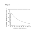
- Figure 17 is a graph showing an example of the relation between the current density and the external quantum efficiency in the GaN-based semiconductor light emitting device shown in Figure 16 . As shown in Figure 17 , an increase in current density decreases the external quantum efficiency in the GaN-based semiconductor light emitting device, due to the band bending B 1 and B2 explained above.
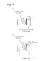
- Figure 18(a) is a conceptual diagram showing accumulation of carriers (Carr) around a dislocation D under relatively low current injection in the GaN-based semiconductor light emitting device, and Figure 18(b) under relatively high current injection.
- a vertical axis represents the value of energy
- the horizontal axis represents the position.
- An object of the present invention conceived to address the problems above, is to provide a GaN-based semiconductor light emitting device having an active layer containing indium, in which a decrease in quantum efficiency under high current injection is moderated, and to provide a method for making the same.
- a GaN-based semiconductor light emitting device includes (a) a substrate comprising a first GaN-based semiconductor in which a primary surface of the substrate tilts from a plane normal to a reference axis [0 0 0 1] or [0 0 0 -1] of the first GaN-based semiconductor toward the m-axis of the first GaN-based semiconductor at a tilt angle in the range of 63 degrees to below 80 degrees; (b) a GaN-based semiconductor epitaxial region disposed on the primary surface; (c) an active layer disposed on the GaN-based semiconductor epitaxial region; (d) an electron blocking layer disposed on the active layer; and (e) a contact layer disposed on the electron blocking layer.
- the active layer comprises a second GaN-based semiconductor, and the second GaN-based semiconductor contains indium.
- the electron blocking layer comprises a third GaN-based semiconductor, and the bandgap of the third GaN-based semiconductor is larger than the bandgap of the second GaN-based semiconductor.
- the contact layer comprises a fourth GaN-based semiconductor, and the bandgap of the fourth GaN-based semiconductor is equal to or smaller than the bandgap of the third GaN-based semiconductor.
- the dislocation density in the first GaN-based semiconductor of the substrate is 1 ⁇ 10 7 cm -2 or less.
- a method for making a GaN-based light emitting device includes the steps of (f) growing a GaN-based semiconductor epitaxial region on a primary surface of a wafer comprising a first GaN-based semiconductor; (g) growing an active layer on the GaN-based semiconductor epitaxial region; (h) growing an electron blocking layer on the active layer; and (i) growing a contact layer on the electron blocking layer.
- the primary surface of the wafer tilts from a plane normal to a reference axis [0 0 0 1] or [0 0 0 -1] of the first GaN-based semiconductor toward the m-axis of the first GaN-based semiconductor at a tilt angle in the range of 63 degrees to below 80 degrees.
- the active layer comprises a second GaN-based semiconductor, and the second GaN-based semiconductor contains indium.
- the electron blocking layer comprises a third GaN-based semiconductor, and the bandgap of the third GaN-based semiconductor is larger than the bandgap of the second GaN-based semiconductor.
- the contact layer comprises a fourth GaN-based semiconductor, and the bandgap of the fourth GaN-based semiconductor is equal to or smaller than the bandgap of the third GaN-based semiconductor.
- the dislocation density in the first GaN semiconductor of the wafer is 1 ⁇ 10 7 cm -2 or less.
- the substrate comprises the first GaN-based semiconductor.
- the primary surface of the substrate tilts from the plane normal to the axis [0001] or [000-1] of the first GaN-based semiconductor (c-plane) toward the m-axis of the first GaN-based semiconductor at a tilt angle in the range of 63 degrees to below 80 degrees.
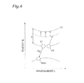
- anisotropic strain is induced. This anisotropic strain shifts the energy level E3 resonantly inducing an Auger process. This can prevent an Auger process for an energy gap Eg, which corresponds to emission of light ranging from blue to green.
- the Auger process is prevented for a possible bandgap of a GaN-based semiconductor which emits light ranging from blue to green, the droop phenomenon caused by the Auger process can be suppressed, and a decrease in quantum efficiency under high current injection can be moderated in a GaN-based semiconductor light emitting device including an active layer containing indium.
- the primary surface of the substrate tilts from the c-plane of the first GaN semiconductor toward the m-axis at a tilt angle in the range of 63 degrees to below 80 degrees.
- the band bending B1 and B2 shown in Figure 16(a) turns to the opposite direction.
- the dislocation density in the first GaN-based semiconductor of the substrate is 1 ⁇ 10 -7 cm -2 or less.
- the GaN-based semiconductor epitaxial region, the active layer, the electron blocking layer, and the contact layer are disposed on the substrate comprising the high-quality GaN-based semiconductor having such a low dislocation density. Since the dislocation density is low in the GaN-based semiconductor light emitting device, trapping of carriers at dislocation can be reduced even under relatively high current injection, thereby moderating a decrease in quantum efficiency.
- the GaN-based semiconductor light emitting device and the method for making the GaN-based semiconductor light emitting device can solve the disadvantages of a conventional GaN-based semiconductor light emitting device, such as (1) the Auger process, (2) the depletion of holes caused by an electron blocking layer, and (3) a high dislocation density characteristic to a GaN-based light emitting device, thereby effectively moderating a decrease in quantum efficiency.
- the primary surface of the substrate preferably tilts at an angle of 70 degrees or more.
- the active layer is preferably provided so as to emit light of a wavelength range of 400 nm to 650 nm. More preferably, the active layer is provided so as to emit light of a wavelength range of 440 nm to 540 nm. More preferably, the active layer is provided so as to emit light of a wavelength range of 440 nm to 490 nm.
- the tilt angle of the substrate in the range of 63 degrees to below 80 degrees is particularly effective for the light emission in these wavelength ranges.
- the GaN-based semiconductor light emitting device and the method for making the GaN-based semiconductor light emitting device may be characterized in that the second GaN-based semiconductor has a composition of In x2 Al y2 Ga 1-x2-y2 N (0 ⁇ x2 ⁇ 1, 0 ⁇ y2 ⁇ 1). This enables a lattice constant in the active layer to be freely chosen within a certain range and thus the magnitude of anisotropic strain in the active layer to be controlled preferably. As a result, the energy gasp ⁇ between the energy level E3 and the bottom energy of the conduction band, which are shown in Figure 14(b) , can be effectively controlled.
- the third GaN-based semiconductor preferably has a composition of In x3 Al y3 Ga 1-x3-y3 N (0 ⁇ x3 ⁇ 1, 0 ⁇ y3 ⁇ 1), and a lattice constant is equal to or smaller than the lattice constant in the first GaN-based semiconductor.
- the GaN-based semiconductor light emitting device and the method for making the GaN-based semiconductor light emitting device may be characterized in that the GaN-based semiconductor light emitting device is a light emitting diode.
- the planar chip size of the light emitting diode is preferably smaller than 500 ⁇ m square.
- the device since a decrease in quantum efficiency due to a droop phenomenon is effectively moderated, the device can have high efficiency of light emission under a high current density, resulting in downsizing of the chip.
- the GaN-based semiconductor light emitting device of the present invention since the GaN-based semiconductor light emitting device comprises an active layer containing indium, a decrease in quantum efficiency under high current injection can be moderated.
- a GaN-based semiconductor light emitting device and a method for making the same according to the present invention is explained in detail below, with reference to the accompanying drawings.
- the elements are referred to by the same reference numerals to eliminate duplicated explanation.
- crystallographic axes of a hexagonal crystal are represented by the a1-axis, a2-axis, a3-axis, and c-axis.
- a direction opposite to a positive direction along the crystallographic axis is represented by a minus sign (for example "-1") appended to the numeral (for example "1").
- the axis [0 0 0 -1] refers to the direction opposite to the axis [000 1].
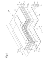
- Figure 1 is a schematic view showing a structure of a GaN-based semiconductor light emitting device 11a according to an embodiment of the present invention.
- Examples of the GaN-based semiconductor light emitting device 11a include a light emitting diode.
- a GaN-based semiconductor light emitting device 11a includes a substrate 13, a GaN-based semiconductor epitaxial region 15, and an active layer 17.
- the substrate 13 comprises a first GaN-based semiconductor.
- the first GaN-based semiconductor may be composed of GaN, InGaN, AlGaN, and InAlGaN.
- GaN one of the binary GaN-based semiconductors, can have high-quality crystallinity and a stable primary surface as a substrate.
- the first GaN-based semiconductor of the substrate 13 has a dislocation density of 1 ⁇ 10 7 cm -2 or less.
- the first GaN-based semiconductor may include, for example, AlN.
- the c-axis of the substrate 13 extends along a plane Sc shown in Figure 1 .
- a coordinate system CR (c-axis, a-axis, m-axis) is illustrated on the plane Sc, each axis representing the crystallographic axis of the hexagonal GaN-based semiconductor.
- Figure 1 also illustrates a reference axis Cx extending along the c-axis of the first GaN semiconductor.
- the reference axis Cx refers to the axis [0001] or the axis [000-1] of the first GaN-based semiconductor.
- a vector VC+ along the reference axis Cx points in the direction of the axis [0 0 0 1], and a vector VC- in the direction of the axis [0 0 0 -1].
- the primary surface 13a of the substrate 13 tilts from a plane (c-plane) normal to the reference axis Cx toward the m-axis of the first GaN-based semiconductor at a tilt angle ⁇ of more than or equal to 63 degrees and less than 80 degrees.
- the tilt angle ⁇ is 70 degrees or more.
- the tilt angle ⁇ is defined by the normal vector VN of the primary surface 13a and the reference axis Cx in the substrate 13.
- the angle ⁇ is equal to the angle defined by the vector VC+ and the vector VN.
- the tilt angle ⁇ is preferably 75 degrees.
- the primary surface 13a corresponds to the plane ⁇ 20-21 ⁇ of the hexagonal GaN-based semiconductor.
- a GaN-based semiconductor epitaxial region 15 is provided on the primary surface 13a.
- the GaN-based semiconductor epitaxial region 15 may include one or more first conductive type GaN-based semiconductor layers.
- the GaN-based semiconductor epitaxial region 15 includes an n-type GaN semiconductor layer 23.
- the GaN-based semiconductor epitaxial region 15 is provided on the substrate 13, the crystallographic axes in the GaN-based semiconductor epitaxial region 15 are aligned to the crystallographic axes of the substrate 13.
- a primary surface 15a of the GaN-based semiconductor epitaxial region 15 also tilts from the plane normal to the reference axis Cx toward the m-axis at an angle of more than or equal to 63 degrees and less than 80 degrees.
- the active layer 17 is provided on the GaN-based semiconductor epitaxial region 15.
- the active layer 17 is composed of a second GaN-based semiconductor containing indium.
- the second GaN-based semiconductor has a composition of In x2 Al y2 Ga 1-x2-y2 N (0 ⁇ x2 ⁇ 1, 0 ⁇ y2 ⁇ 1).
- the direction normal to the surface of the active layer 17 tilts relative to the reference axis Cx.
- the crystallographic axes of the active layer 17 are aligned to the crystallographic axes of the substrate 13 through the GaN-based semiconductor epitaxial region 15.
- the primary surface of the active layer 17 also tilts from the plane normal to the reference axis Cx toward the m-axis at an angle of more than or equal to 63 degrees and less than 80 degrees.
- the active layer 17 is preferably provided so as to emit light of a wavelength of 400 nm or more.
- the active layer 17 is preferably provided so as to emit light of a wavelength of 650 nm or less. In an active layer emitting light of a wavelength of 650 nm or more, desired crystalline quality is not readily achieved because of a large amount of indium in the composition. More preferably, the active layer 17 is provided so as to emit light of a wavelength of more than or equal to 440 nm and less than or equal to 540 nm. More preferably, the active layer 17 is provided so as to emit light of a wavelength of more than or equal to 440 nm and less than or equal to 490 nm.
- the tilt angle of the primary surface of the active layer 17 in the range of 63 degrees to below 80 degrees is particularly effective for the light emission in these wavelength ranges.
- the active layer 17 may have a quantum well structure 31.
- the quantum well structure 31 may include well layers 33 and barrier layers 35 alternately arranged in the direction of a predetermined axis Ax.
- the well layers 33 and the barrier layers 35 are each composed of a second GaN-based semiconductor containing indium, for example, In x2 Al y2 Ga 1-x2-y2 N (0 ⁇ x2 ⁇ 1, 0 ⁇ y2 ⁇ 1).
- the bandgap of the barrier layer 35 is larger than the bandgap of the well layer 33.
- the n-type GaN semiconductor layer 23, the active layer 17, an electron blocking layer 27, and a contact layer 29 are arranged along the predetermined axis Ax.
- the direction of the reference axis Cx is different from the direction of the predetermined axis Ax.
- Figure 1 illustrates a coordinate system S.
- the primary surface 13a of the substrate 13 is normal to the Z-axis of the coordinate system S, and extends along the X-axis and the Y-axis.
- the X-axis points in the direction of the a-axis.
- the GaN-based semiconductor light emitting device 11a includes a GaN-based semiconductor region 21 disposed on the active layer 17.
- the GaN-based semiconductor region 21 includes one or more second conductive type GaN-based semiconductor layers.
- the GaN-based semiconductor region 21 includes the electron blocking layer 27 provided on the active layer 17, and the contact layer 29 provided on the electron blocking layer 27.
- the electron blocking layer 27 is composed of a third GaN-based semiconductor.
- the third GaN-based semiconductor has a bandgap larger than the bandgap of the second GaN-based semiconductor of the active layer 17.
- the third GaN-based semiconductor is composed of p-type In x3 Al y3 Ga 1-x3-y3 N (0 ⁇ x3 ⁇ 1, 0 ⁇ y3 ⁇ 1), and more preferably the third GaN-based semiconductor is composed of p-type In x3 Al y3 Ga 1-x3-y3 N (0 ⁇ x3 ⁇ 1, 0 ⁇ y3 ⁇ 1).
- the lattice constant of the third GaN-based semiconductor may be equal to or smaller than the lattice constant of the first GaN-based semiconductor of the substrate 13.
- the contact layer 29 is composed of a fourth GaN-based semiconductor.
- the bandgap of the fourth GaN-based semiconductor is preferably equal to or less than the bandgap of the third GaN-based semiconductor.
- the fourth GaN-based semiconductor is composed of p-type In x4 Al y4 Ga 1-x4-y4 N (0 ⁇ x4 ⁇ 1, 0 ⁇ y4 ⁇ 1), and more preferably the fourth GaN-based semiconductor is composed of p-type In x4 Al y4 Ga 1-x4-y4 N (0 ⁇ x4 ⁇ 1, 0 ⁇ y4 ⁇ 1).
- the crystallographic axes of the electron blocking layer 27 and the contact layer 29 are aligned to the crystallographic axes of the substrate 13 through the active layer 17 and the GaN-based semiconductor epitaxial region 15.
- the primary surfaces of the electron blocking layer 27 and the contact layer 29 also tilt from the plane normal to the reference axis Cx toward the m-axis at an angle of more than or equal to 63 degrees and less than 80 degrees.
- the GaN-based semiconductor light emitting device 11a may include a first electrode 37 (for example, an anode) disposed on the contact layer 29.
- the first electrode 37 may include a transparent electrode covering the contact layer 29.
- the transparent electrode may be composed of, for example, Ni/Au.
- the GaN-based semiconductor light emitting device 11a may include a second electrode 39 (for example, a cathode) provided on a back surface 13b of the substrate 13.
- the second electrode 39 may be composed of, for example, Ti/Al.
- the active layer 17 emits light L1 in response to an external voltage applied between the electrodes 37 and 39.
- the GaN-based semiconductor light emitting device 11a may include a surface-emitting device.
- FIG 2 is a schematic view showing a structure of a GaN-based semiconductor light emitting device 11b according to another embodiment of the present invention.
- the GaN-based semiconductor light emitting device 11b may include, for example, a semiconductor laser.
- the GaN-based semiconductor light emitting device 11b includes a substrate 13, a GaN-based semiconductor epitaxial region 15, and an active layer 17, like the GaN-based semiconductor light emitting device 11 a shown in Figure 1 .
- the substrate 13 is composed of a first GaN-based semiconductor, for example, GaN, InGaN, AlGaN, or InAlGaN.
- the first GaN-based semiconductor of the substrate 13 has a dislocation density of 1 ⁇ 10 7 cm -2 or less.
- the first GaN-based semiconductor may be composed of, for example, AlN.
- the c-axis of the substrate 13 extends along a plane Sc shown in Figure 2 .
- a coordinate system CR (c-axis, a-axis, m-axis) is illustrated on the plane Sc.
- a reference axis Cx is also illustrated.
- the reference axis Cx refers to the axis [0 0 0 1] or [000-1] of the first GaN-based semiconductor.
- a vector VC+ along the reference axis Cx points in the direction of the axis [0 0 0 1], and a vector VC- in the direction of the axis [000-1].
- the primary surface 13a of the substrate 13 tilts from a plane (c-plane) normal to the reference axis Cx toward the m-axis of the first GaN-based semiconductor at a tilt angle ⁇ of more than or equal to 63 degrees and less than 80 degrees.
- the tilt angle ⁇ is defined by the normal vector VN of the primary surface 13a and the reference axis Cx in the substrate 13. In the embodiment, the angle ⁇ is equal to the angle defined by the vector VC+ and the vector VN.
- the GaN-based semiconductor epitaxial region 15 is provided on the primary surface 13a.
- the GaN-based semiconductor epitaxial region 15 may include one or more first conductive type GaN-based semiconductor layers.
- the GaN-based semiconductor epitaxial region 15 includes an n-type cladding layer 41 and a light guiding layer 43a arranged in the direction of the Ax axis (Z-direction).
- the n-type cladding layer 41 may be composed of, for example, AlGaN, GaN, or InAlGaN.
- the light guiding layer 43 a may be composed of, for example, undoped InGaN.
- the primary surface 15a of the GaN-based semiconductor epitaxial region 15 also tilts from the plane normal to the reference axis Cx toward the m-axis at an angle of more than or equal to 63 degrees and less than 80 degrees.
- the active layer 17 is provided on the GaN-based semiconductor epitaxial region 15.
- the active layer 17 is composed of a second GaN-based semiconductor containing indium.
- the second GaN-based semiconductor has a composition of In x2 Al y2 Ga 1-x2-y2 N (0 ⁇ x2 ⁇ 1, 0 ⁇ y2 ⁇ 1).
- the direction normal to the surface of the active layer 17 tilts relative to the reference axis Cx.
- the crystallographic axes of the active layer 17 are aligned to the crystallographic axes of the substrate 13 through the GaN-based semiconductor epitaxial region 15.
- the primary surface of the active layer 17 also tilts from the plane normal to the reference axis Cx toward the m-axis at an angle of more than or equal to 63 degrees and less than 80 degrees.
- the active layer 17 is preferably provided so as to emit light of a wavelength of 400 nm or more.
- the active layer 17 is preferably provided so as to emit light of a wavelength of 650 nm or less. In an active layer emitting light of a wavelength of 650 nm or more, desired crystalline quality is not readily achieved because of a large amount of indium in the composition. More preferably, the active layer 17 is provided so as to emit light of a wavelength of more than or equal to 440 nm and less than or equal to 540 nm. More preferably, the active layer 17 is provided so as to emit light of a wavelength of more than or equal to 440 nm and less than or equal to 490 nm.
- the tilt angle of the primary surface of the active layer 17 in the range of 63 degrees to below 80 degrees is particularly effective for light emission in these wavelength ranges.
- the active layer 17 may have a quantum well structure 31.
- the quantum well structure 31 includes well layers 33 and barrier layers 35 alternately arranged in the direction of a predetermined axis Ax.
- the well layers 33 and the barrier layers 35 are each composed of a second GaN-based semiconductor containing indium, for example, In x2 Al y2 Ga 1-x2-y2 N (0 ⁇ x2 ⁇ 1, 0 ⁇ y2 ⁇ 1).
- the bandgap of the barrier layer 35 is larger than the bandgap of the well layer 33.
- the thickness of the well layer 33 may range, for example, from 0.5 nm to 10 nm.
- the amount of indium in the composition may range from 0.01 to 0.50.
- the GaN-based semiconductor light emitting device 11b has a GaN-based semiconductor region 21 provided on the active layer 17.
- the GaN-based semiconductor region 21 includes one or more GaN-based semiconductor layers.
- the GaN-based semiconductor region 21 includes a light guiding layer 43b, an electron blocking layer 45, a cladding layer 47, and a contact layer 49, arranged in the Z-direction.
- the light guiding layer 43b may be composed of, for example, undoped InGaN.
- the electron blocking layer 45 is composed of a third GaN-based semiconductor.
- the third GaN-based semiconductor has a bandgap larger than the bandgap of the second GaN-based semiconductor of the active layer 17.
- the third GaN-based semiconductor is composed of p-type In x3 Al y3 Ga 1-x3-y3 N (0 ⁇ x3 ⁇ 1, 0 ⁇ y3 ⁇ 1), and more preferably the third GaN-based semiconductor is composed of p-type In x3 Al y3 Ga 1-x3-y3 N (0 ⁇ x3 ⁇ 1, 0 ⁇ y3 ⁇ 1).
- the lattice constant of the third GaN-based semiconductor may be equal to or smaller than that of the first GaN-based semiconductor of the substrate 13.
- the cladding layer 47 may be composed of, for example, p-type AlGaN, p-type GaN, or p-type InAlGaN.
- the contact layer 49 is composed of a fourth GaN-based semiconductor.
- the bandgap of the fourth GaN-based semiconductor is preferably equal to or less than the bandgap of the third GaN-based semiconductor.
- the fourth GaN-based semiconductor is composed of p-type In x4 Al y4 Ga 1-x4-y4 N (0 ⁇ x4 ⁇ 1, 0 ⁇ y4 ⁇ 1), and more preferably the fourth GaN-based semiconductor is composed of p-type In x4 Al y4 Ga 1-x4-y4 N (0 ⁇ x4 ⁇ 1, 0 ⁇ y4 ⁇ 1).
- the electron blocking layer 45, the cladding layer 47, and the contact layer 49 are provided on the active layer 17, the crystallographic axes of the electron blocking layer 45, the cladding layer 47, and the contact layer 49 are aligned to the crystallographic axes of the substrate 13 through the active layer 17 and the GaN-based semiconductor epitaxial region 15.
- the primary surfaces of the electron blocking layer 45, the cladding layer 47, and the contact layer 49 also tilt from the plane normal to the reference axis Cx toward the m-axis at an angle of more than or equal to 63 degrees and less than 80 degrees.
- the GaN-based semiconductor light emitting device 11b may include a first electrode 51 (for example, an anode) provided on the contact layer 49.
- the first electrode 51 is connected to the contact layer 49 through a stripe window of an insulating layer 50 covering the contact layer 49.
- the first electrode 51 may be composed of, for example, Ni/Au.
- the GaN-based semiconductor light emitting device 11b may include a second electrode 52 (for example, a cathode) provided on a back surface 13b of the substrate 13.
- the second electrode 52 may be composed of, for example, Ti/Al.
- the active layer 17 emits light L2 in response to an external voltage applied between the electrodes 51 and 52.
- the GaN-based semiconductor light emitting device may include an edge emitting device.
- the Z component (the component parallel to the predetermined axis Ax) of the piezoelectric field is aligned opposite to the direction from the p-type GaN-based semiconductor layers 45, 47 and 49 toward the n-type cladding layer 41.
- the wavelength shift of emitted light can be reduced.
- FIG. 3 is a flowchart showing the steps of making the GaN-based semiconductor light emitting device 11a.
- the GaN-based semiconductor light emitting device 11a is fabricated by metalorganic vapor phase epitaxy.
- metalorganic vapor phase epitaxy For the epitaxial growth, trimethylgallium (TMG), trimethylindium (TMI), trimethylaluminum (TMA), ammonia (NH 3 ), silane (SiH 4 ), and Bis(cyclopentadienyl)magnesium (Cp 2 Mg) are used as materials.
- a wafer composed of a first GaN-based semiconductor is prepared in Step S101.
- the primary surface of the wafer tilts from a plane normal to the reference axis referring to the crystallographic axis [0 0 0 1] or [0 0 0 -1] of a GaN-based semiconductor (i.e., c-plane) at a tilt angle of more than or equal to 63 degrees and less than 80 degrees.
- the dislocation density in the first GaN-based semiconductor of the wafer is 1 ⁇ 10 7 m -2 or less. This wafer corresponds to the substrate 13 in the embodiment explained above.
- Step S102 the wafer prepared in Step S101 is set in a growth furnace (Step S102).
- a GaN-based semiconductor epitaxial region 15 is grown on the primary surface of the wafer (Step S104).
- a Si-doped GaN layer is grown at 1000°C under supply of TMG, NH 3 , and SiH 4 into the growth furnace.
- the thickness of the Si-doped GaN layer is, for example, 2 ⁇ m.
- an active layer 17 is grown on the GaN-based semiconductor epitaxial region 15 (Step S105).
- a barrier layer 35 composed of In x2 Al y2 Ga 1-x2-y2 N (0 ⁇ x2 ⁇ 1, 0 ⁇ y2 ⁇ 1) is grown on the GaN-based semiconductor epitaxial region 15 (Step S106).
- the barrier layer 35 of undoped InAlGaN is grown by supplying TMG, TMI, TMA, and NH 3 into the growth furnace.
- the thickness of the barrier layer 35 is, for example, 15 nm.
- a well layer 33 of In x2 Al y2 Ga 1-x2-y2 N (0 ⁇ x2 ⁇ 1, 0 ⁇ y2 ⁇ 1) having a bandgap smaller than the bandgap of the barrier layer 35 is grown on the barrier layer 35 (Step S107).
- the well layer 33 of undoped InAlGaN is grown by supplying TMG, TMI, TMA, and NH 3 into the growth furnace (Step S107).
- the thickness of the well layer 33 is, for example, 3 nm.
- the amounts of In and Al in the composition of the undoped InAlGaN well layer 33 are adjusted to achieve a desired emission wavelength.
- a multiquantum well structure 31 is then formed by alternately growing the barrier layers 35 and the well layers 33 (Step S108).
- an electron blocking layer 27 of p-type In x3 Al y3 Ga 1-x3-y3 N (0 ⁇ x3 ⁇ 1, 0 ⁇ y3 ⁇ 1) is grown on the active layer 17 (Step S109).
- the electron blocking layer 27 of p-type AlGaN is grown, for example, by supplying TMG, TMA, NH 3 , and Cp 2 Mg into the growth furnace.
- the electron blocking layer 27 is, for example, 20 nm thick.
- the bandgap of the electron blocking layer 27 is larger than the bandgap of the active layer 17.
- the lattice constant of the electron blocking layer 27 is equal to or less than the lattice constant of the substrate 13.
- a contact layer 29 composed of p-type In x4 Al y4 Ga 1-x4-y4 N (0 ⁇ x4 ⁇ 1, 0 ⁇ y4 ⁇ 1) is grown on the electron blocking layer 27 (Step S110).
- the contact layer 29 of p-type GaN is grown, for example, by supplying TMG, NH 3 , and Cp 2 Mg into the growth furnace.
- the contact layer 29 is, for example, 50 nm thick.
- the bandgap of the contact layer 29 is equal to or smaller than the bandgap of the electron blocking layer 27.
- Electrodes are formed on the epitaxial wafer prepared in the steps above (Step S111).
- a transparent electrode (Ni/Au) 37 is formed on the contact layer 29.
- a pad electrode (Ti/Au) is then formed on the transparent electrode 37.
- An electrode (Ti/Al) 39 is also formed on a back surface of the substrate.
- the electrodes 37 and 39 are heat-treated (annealed).
- the substrate 13 (or the wafer) of the first GaN-based semiconductor is used.
- the primary surface 13a of the substrate 13 tilts from the plane normal to the axis [0 0 0 1] or [0 00-1] of the first GaN semiconductor (i.e., c-plane) toward the m-axis at a tilt angle ⁇ of more than or equal to 63 degrees and less than 80 degrees.
- anisotropic strain is induced.
- this anisotropic strain shifts the energy level E3 resonantly inducing an Auger process, resulting in a change in the energy gap ⁇ between the energy level E3 and the bottom of the conduction band.
- Such energy gap Eg of the GaN-based semiconductor does not cause an Auger process. That is, the Auger process is prevented within a possible bandgap range of the GaN-based semiconductor containing indium which emits light ranging from blue to green.
- the droop phenomenon caused by the Auger process can be suppressed, a decrease in quantum efficiency under high current injection can be moderated in the GaN-based semiconductor light emitting devices 11a and 11b provided with the active layer 17 containing indium.
- the amplitude of the anisotropic strain induced in the well layer 33 can be controlled by adjusting compositions of the well layer 33 and the barrier layer 35.
- the well layer 33 normally has compressive strain, but may have tensile strain by changing the compositions. This may modify the band structure of the conduction band.
- the droop phenomenon can be effectively suppressed for the emission at a wavelength range of 440 nm to 540 nm.
- the primary surface 13a of the substrate 13 tilts from the c-axis of the GaN-based semiconductor toward the m-axis of the GaN-based semiconductor at a tilt angle ⁇ of more than or equal to 63 degrees and less than 80 degrees.
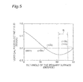
- Figure 5 is a graph showing the relation between the tilt angle ⁇ of the primary surface and the piezoelectric field in the active layer 17.
- the piezoelectric field in the active layer 17 also takes a negative value. That is, according to the embodiment, the direction of the piezoelectric field in the active layer 17 is opposite to the direction of an electric field induced by current injection.
- the dislocation density in the first GaN-based semiconductor of the substrate 13 is 1 ⁇ 10 -7 cm -2 or less.
- the GaN-based semiconductor epitaxial region 15, the active layer 17, the electron blocking layer 27, and the contact layer 29 are disposed on the substrate 13 composed of the high-quality GaN-based semiconductor having such a low dislocation density.
- the dislocation density is low in the GaN-based semiconductor light emitting device 11a, trapping of carriers in dislocation can be reduced even under relatively high current injection, thereby moderating a decrease in quantum efficiency.
- the GaN-based semiconductor light emitting devices 11a and 11b and the method for making the GaN-based semiconductor light emitting device 11a can solve disadvantages of a conventional GaN-based semiconductor light emitting device, such as (1) the Auger process, (2) the depletion of holes caused by an electron blocking layer, and (3) a high dislocation density characteristic to a GaN-based light emitting device, thereby effectively moderating a decrease in quantum efficiency under high current injection.
- the second GaN-based semiconductor of the active layer 17 preferably has a composition of In x2 Al y2 Ga 1-x2-y2 N (0 ⁇ x2 ⁇ 1, 0 ⁇ y2 ⁇ 1).
- Figure 6 is a graph showing the relation between the lattice constant and the band-edge energy of the GaN-based semiconductor.
- the lattice constant in the active layer 17 of In x2 Al y2 Ga 1-x2-y2 N (0 ⁇ x2 ⁇ 1, 0 ⁇ y2 ⁇ 1) can be freely chosen within a certain range by desirably modifying the amounts of indium (x2) and aluminum (y2) in the composition.
- the energy gap ⁇ between the energy level E3 and the bottom energy of the conduction band shown in Figure 4 , can be effectively controlled.
- the GaN-based semiconductor light emitting device may be a light emitting diode, like the GaN-based semiconductor light emitting device 11a.
- a planar chip size of the light emitting diode is preferably smaller than 500 ⁇ m square.
- the device since a decrease in quantum efficiency due to the droop phenomenon is effectively moderated, the device can have high efficiency of light emission under a high current density, resulting in downsizing of the chip.
- a GaN-based semiconductor light emitting device 11c having a cross-sectional structure shown in Figure 7 was fabricated using a GaN substrate having a dislocation density of 1 ⁇ 10 7 cm -2 or less and a primary surface tilting from the c-plane toward the m-axis at a tilt angle of 75 degrees, through the steps described below.
- NH 3 , TMG, TMI, TMA, and Cp 2 Mg were used as source materials.
- an n-type GaN buffer layer 54 having a thickness of 2 ⁇ m was grown on a primary surface 53a of the substrate 53 at 1000°C.
- An undoped GaN barrier layer 55 was grown at a reduced temperature of 870°C, and an undoped In 0.15 Ga 0.85 N well layer 56 was grown at 780°C.
- a multiquantum well structure 57 having three periodicities was formed.
- a p-type Al 0.18 Ga 0.82 N electron blocking layer 58 having a thickness of 20 nm was grown on the active layer 57 at an elevated temperature of 1000°C.
- a p-type GaN contact layer 59 was grown on the electron blocking layer 58, and then the epitaxial wafer was brought out from the growth furnace after cooling.
- a Ni/Au electrode 60 was then deposited on the p-type GaN contact layer 59, and a Ti/Al electrode 61 on the back surface 53b of the substrate 53.
- the GaN-based semiconductor light emitting device 11c was completed by dicing the epitaxial wafer into individual chips. The shape of the device viewed from the top was a 400 ⁇ m square.
- a GaN-based semiconductor light emitting device 11d having a cross-sectional structure shown in Figure 8 was fabricated using a sapphire substrate having the c-plane as a primary surface through the following steps.
- a low-temperature buffer layer 74 having a thickness of 50 nm was grown on a primary surface 73a of a sapphire substrate 73 at 475°C and an n-type GaN buffer layer 75 having a thickness of 5 ⁇ m was grown on the low-temperature buffer layer 74 at 1050°C.
- An undoped GaN barrier layer 76 was grown at a reduced temperature of 870°C, and an undoped In 0.15 Ga 0.85 N well layer 77 was grown at 780°C. By repeating these steps, a multiquantum well structure 78 having three periodicities was formed. Subsequently, p-type Al 0 .
- a Ni/Au electrode 81 was deposited on the p-type GaN contact layer 80, and a Ti/Al electrode 82 on the exposed surface of the n-type GaN buffer layer 75.
- the GaN-based semiconductor light emitting device 11d was completed by dicing the epitaxial wafer into individual chips. For precise comparison, the fabrication process was modified to achieve light extraction efficiency close to the light extraction efficiency of the GaN-based semiconductor light emitting device 11c. The emission wavelengths were 460 nm in the GaN-based semiconductor light emitting devices 11c and 11d.
- Figure 9 shows the results of the measurements.
- a current density (a horizontal axis) ranges from 0 to 300 A/cm 2 .
- a current density (a horizontal axis) ranges from 0 to 1200 A/cm 2 .
- the lines G11 represent a characteristic curve of the GaN-based semiconductor light emitting device 11c (the low dislocation density semipolar GaN substrate was used), and the lines G12 represent a characteristic curve of the GaN-based semiconductor light emitting device 11d (the c-plane sapphire substrate was used).
- the GaN-based semiconductor light emitting device 11d (the c-plane sapphire substrate) has higher external quantum efficiency than the GaN-based semiconductor light emitting device 11c (the low dislocation density semipolar GaN substrate) at an injected current of 1 A/cm 2 .
- the GaN-based semiconductor light emitting device 11c (the low dislocation density semipolar GaN substrate) has higher external quantum efficiency than the GaN-based semiconductor light emitting device 11d (the c-plane sapphire substrate).
- the difference in the quantum efficiency between the GaN-based quantum light emitting devices 11c and 11d is increased as the injected current increases.
- the external quantum efficiency decreases to about 1/2 to about 1/3 in the GaN-based semiconductor light emitting device 11d (the c-plane sapphire substrate).
- the external quantum efficiency decreases merely to about 2/3 to 1/2.
- GaN-based semiconductor light emitting devices 11c and 11d respectively provided with well layers 56 ( Figure 7 ) and well layers 77 ( Figure 8 ) were fabricated, each well layer having a different composition from the GaN-based semiconductor light emitting devices in Example 1.
- the well layers 56 and the well layers 77 having a composition of In 0.18 Ga 0.82 N were grown at 760°C.
- the emission wavelengths were 480 nm.
- the well layers 56 and the well layers 77 having a composition of In 0.22 Ga 0.78 N were grown at 740°C.
- the emission wavelengths were 500 nm.
- the well layers 56 and the wall layers 77 having a composition of In 0.28 G 0.72 N were grown at 720°C.
- the emission wavelengths were 520 nm.
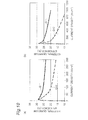
- Figures 10 to 12 are graphs showing the dependence of the external quantum efficiency on the current density in the GaN-based semiconductor light emitting devices.
- Figures 10 to 12 correspond to Examples A to C, respectively.
- the current density (horizontal axes) ranges from 0 to 300 A/cm 2 .
- the current density (horizontal axes) ranges from 0 to 1200 A/cm 2 .
- the lines G11 represent a characteristic curve of the GaN-based semiconductor light emitting device 11c (the low dislocation density semipolar GaN substrate was used)
- the lines G12 represent a characteristic curve of the GaN-based semiconductor light emitting device 11d (the c-plane sapphire substrate was used).
- Example 1 As shown in Figures 10 to 12 , the effects explained in Example 1 are remarkably exhibited by the GaN-based semiconductor light emitting devices provided with the well layers having different compositions. That is, in the GaN-based semiconductor light emitting device 11c, the droop phenomenon is effectively suppressed.
- a GaN-based semiconductor light emitting device having an active layer containing indium and a method for making the same can be provided, in which a decrease in quantum efficiency under high current injection can be moderated.
Landscapes
- Physics & Mathematics (AREA)
- Optics & Photonics (AREA)
- Engineering & Computer Science (AREA)
- Condensed Matter Physics & Semiconductors (AREA)
- General Physics & Mathematics (AREA)
- Electromagnetism (AREA)
- Nanotechnology (AREA)
- Chemical & Material Sciences (AREA)
- Biophysics (AREA)
- Crystallography & Structural Chemistry (AREA)
- Life Sciences & Earth Sciences (AREA)
- Led Devices (AREA)
- Semiconductor Lasers (AREA)
Abstract
A GaN-based semiconductor light emitting device 11a includes a substrate 13 composed of a GaN-based semiconductor having a primary surface 13a tilting from the c-plane toward the m-axis at a tilt angle α of more than or equal to 63 degrees and less than 80 degrees, a GaN-based semiconductor epitaxial region 15, an active layer 17, an electron blocking layer 27, and a contact layer 29. The active layer 17 is composed of a GaN-based semiconductor containing indium. The substrate 13 has a dislocation density of 1 × 107 cm-2 or less. In the GaN-based semiconductor light emitting device 11a provided with the active layer containing indium, a decrease in quantum efficiency under high current injection can be moderated.
Description
- The present invention relates to a GaN-based light emitting device and the method for making the same.
-
Nonpatent Literature 1 discloses that a droop phenomenon in a GaN-based semiconductor light emitting device, that is, a decrease in internal quantum efficiency occurring when an injected current exceeds a threshold value, is attributed mainly to an Auger process. In the literature, an Auger coefficient is measured experimentally. -
Nonpatent Literature 2 discloses that the droop phenomenon in a GaN-based semiconductor light emitting device is attributed mainly to the Auger process. In the literature, a first-principles calculation of an energy band diagram for a GaN-based semiconductor light emitting device indicates the existence of an energy level which resonantly induces the Auger process at a wavelength range of blue to green light. -
Nonpatent Literature 3 discloses that the droop phenomenon in a GaN-based semiconductor light emitting device is attributed to localization of holes at an interface between an electron blocking layer and a contact layer, and a low efficiency of hole injection into an active layer due to the electron blocking layer. - [NPL1] Y C. Shen et al., "Auger recombination in InGaN measured by photoluminescence," Applied Physics Letters, American Institute of Physics, Vol.91, 141101 (2007)
[NPL2] Kris T. Delaney et al., "Auger recombination rates in nitrides from first principles," Applied Physics Letters, American Institute of Physics, Vol.94, 191109 (2009)
[NPL3] Sang-Heon Han et al., "Effect of electron blocking layer on efficiency droop in InGaN/GaN multiple quantum well light-emitting diodes," Applied Physics Letters, American Institute of Physics, Vol.94, 231123 (2009) - In recent years, light emitting devices of GaN-based semiconductor, which have a hexagonal crystal structure, have been extensively studied. The light emitting device is provided with a substrate composed of GaN-based semiconductor, a semiconductor layer of a first conductivity type (for example, n-type), an active layer, and a semiconductor layer of a second conductivity type (for example, p-type); these layers are epitaxially grown in sequence on a primary surface of the substrate. In general, the substrate has a c-plane of a GaN-based semiconductor crystal as the primary surface. The active layer is composed of, for example, a GaN-based semiconductor containing indium in the composition.
-
Figure 13 is a graph showing an example of the relation between the excitation density and the internal quantum efficiency in such a light emitting device. As shown inFigure 13 , in a low current injection region (Region A inFigure 13 ), an increase in current enhances the internal quantum efficiency in the light emitting device, while in a high current injection region (Region B inFigure 13 ) where the injected current exceeds a threshold value, an increase in current reduces the internal quantum efficiency (droop phenomenon). The droop phenomenon is probably caused by the following three reasons: - The Auger process indicates a three-body process in which excessive energy released by recombination of an electron and a hole is spent without for emitting light, but for exciting another electron into another higher energy level. The Auger process is one of the many-body effects, which is resonantly induced by a shortening average distance between excitons when the carrier density becomes high in the light emitting device.
-
Figure 14 includes drawings explaining the Auger process. In a light emitting device, an electron (e1) falls into a hole, which releases energy as emitted light, the released energy being equal to an energy gap (Eg) between the energy levels of a conduction band and a valence band, as shown inFigure 14(a) . In a GaN-based semiconductor, however, another energy level (E3) exists that has an energy gap Δ from a bottom of a conduction band, the energy gap being equivalent to energy of light emission in the range of blue to green light. Thus, the energy released by the fall of the electron (e1) into the hole, which is equivalent to the energy gap (Eg) between the conduction band and the valence band, is spent for exciting another electron (e2) to the energy level (E3). Through these steps, electrons and holes are lost without emitting light, resulting in decreased internal quantum efficiency. -
Figure 15 is a graph showing the relation between the bandgap and the Auger coefficient in a semiconductor. As shown inFigure 15 , the Auger process, explained above, is remarkable in the case where the semiconductor has a bandgap in a certain range having a central value of about 2.5 eV (Range C inFigure 15 ). The bandgap corresponds to an emission wavelength range of 440 nm to 540 nm; such a bandgap is achieved, for example, in a GaN-based semiconductor containing indium. Thus, a GaN-based semiconductor light emitting device containing indium in an active layer disadvantageously has a decrease in internal quantum efficiency due to the Auger process. -
Figure 16(a) shows an example of the energy band diagram in a GaN-based semiconductor light emitting device. The GaN-based light emitting device is provided with an n-type GaN layer, a multiquantum well (MQW) active layer disposed on the n-type GaN layer, an electron blocking layer (EBL) disposed on the active layer, and a p-type GaN layer disposed on the electron blocking layer.Figure 16(b) is a graph showing a depth profile of the carrier density in the GaN-based semiconductor light emitting device. InFigure 16(b) , a line Ge and a line Gh represent an electron density and a hole density, respectively. - As shown in
Figure 16(a) , high-current injection into the GaN-based semiconductor light emitting device having the structure explained above causes bending of the energy band (B1and B2 inFigure 16(a) ) caused by an applied voltage or a piezoelectric field. The band bending B1 at the interface between the electron blocking layer and the p-type GaN layer localizes holes at the interface (peak P3 inFigure 16(b) ). The band bending B2 at the interface between the electron blocking layer and the active layer blocks the injection of holes into the active layer, resulting in decreased quantum efficiency. -
Figure 17 is a graph showing an example of the relation between the current density and the external quantum efficiency in the GaN-based semiconductor light emitting device shown inFigure 16 . As shown inFigure 17 , an increase in current density decreases the external quantum efficiency in the GaN-based semiconductor light emitting device, due to theband bending B 1 and B2 explained above. -
Figure 18(a) is a conceptual diagram showing accumulation of carriers (Carr) around a dislocation D under relatively low current injection in the GaN-based semiconductor light emitting device, andFigure 18(b) under relatively high current injection. InFigures 18(a) and 18(b) , a vertical axis represents the value of energy, and the horizontal axis represents the position. - As shown in
Figure 18(a) , under the relatively low current injection in the GaN-based semiconductor light emitting device (low injection region), carriers (Carr) can move without being trapped in the dislocation D, resulting in efficient light emission. This can be explained by a carrier localization effect due to nonuniformity of the indium distribution in the active layer of the GaN-based semiconductor containing indium. In contrast, under the relatively high current injection in the GaN-based semiconductor light emitting device (high injection region), the carriers (Carr) overflow from the localization site, disappearing without emitting light due to being trapped at the dislocation D. In a GaN-based semiconductor light emitting device, typically having a high dislocation density, the quantum efficiency is decreased by this mechanism. - An object of the present invention, conceived to address the problems above, is to provide a GaN-based semiconductor light emitting device having an active layer containing indium, in which a decrease in quantum efficiency under high current injection is moderated, and to provide a method for making the same.
- To solve the problems mentioned above, a GaN-based semiconductor light emitting device according to the invention includes (a) a substrate comprising a first GaN-based semiconductor in which a primary surface of the substrate tilts from a plane normal to a reference axis [0 0 0 1] or [0 0 0 -1] of the first GaN-based semiconductor toward the m-axis of the first GaN-based semiconductor at a tilt angle in the range of 63 degrees to below 80 degrees; (b) a GaN-based semiconductor epitaxial region disposed on the primary surface; (c) an active layer disposed on the GaN-based semiconductor epitaxial region; (d) an electron blocking layer disposed on the active layer; and (e) a contact layer disposed on the electron blocking layer. The active layer comprises a second GaN-based semiconductor, and the second GaN-based semiconductor contains indium. The electron blocking layer comprises a third GaN-based semiconductor, and the bandgap of the third GaN-based semiconductor is larger than the bandgap of the second GaN-based semiconductor. The contact layer comprises a fourth GaN-based semiconductor, and the bandgap of the fourth GaN-based semiconductor is equal to or smaller than the bandgap of the third GaN-based semiconductor. The dislocation density in the first GaN-based semiconductor of the substrate is 1×107 cm-2 or less.
- According to the present invention, a method for making a GaN-based light emitting device includes the steps of (f) growing a GaN-based semiconductor epitaxial region on a primary surface of a wafer comprising a first GaN-based semiconductor; (g) growing an active layer on the GaN-based semiconductor epitaxial region; (h) growing an electron blocking layer on the active layer; and (i) growing a contact layer on the electron blocking layer. The primary surface of the wafer tilts from a plane normal to a reference axis [0 0 0 1] or [0 0 0 -1] of the first GaN-based semiconductor toward the m-axis of the first GaN-based semiconductor at a tilt angle in the range of 63 degrees to below 80 degrees. The active layer comprises a second GaN-based semiconductor, and the second GaN-based semiconductor contains indium. The electron blocking layer comprises a third GaN-based semiconductor, and the bandgap of the third GaN-based semiconductor is larger than the bandgap of the second GaN-based semiconductor. The contact layer comprises a fourth GaN-based semiconductor, and the bandgap of the fourth GaN-based semiconductor is equal to or smaller than the bandgap of the third GaN-based semiconductor. The dislocation density in the first GaN semiconductor of the wafer is 1×107 cm-2 or less.
- In the GaN-based semiconductor light emitting device and the method for making the GaN-based semiconductor light emitting device explained above, the substrate comprises the first GaN-based semiconductor. The primary surface of the substrate tilts from the plane normal to the axis [0001] or [000-1] of the first GaN-based semiconductor (c-plane) toward the m-axis of the first GaN-based semiconductor at a tilt angle in the range of 63 degrees to below 80 degrees. In the active layer disposed on the semipolar primary surface, anisotropic strain is induced. This anisotropic strain shifts the energy level E3 resonantly inducing an Auger process. This can prevent an Auger process for an energy gap Eg, which corresponds to emission of light ranging from blue to green. That is, since the Auger process is prevented for a possible bandgap of a GaN-based semiconductor which emits light ranging from blue to green, the droop phenomenon caused by the Auger process can be suppressed, and a decrease in quantum efficiency under high current injection can be moderated in a GaN-based semiconductor light emitting device including an active layer containing indium.
- In the GaN-based semiconductor light emitting device and the method for making the GaN-based semiconductor light emitting device, the primary surface of the substrate tilts from the c-plane of the first GaN semiconductor toward the m-axis at a tilt angle in the range of 63 degrees to below 80 degrees. With this range of the tilt angles, since the piezoelectric field in the active layer is negative, the band bending B1 and B2 shown in
Figure 16(a) turns to the opposite direction. Thus, the localization of holes and the blocking of the hole injection into the active layer can be suppressed even under high current injection, thereby moderating a decrease in quantum efficiency. - In the GaN-based semiconductor light emitting device and the method for making the GaN-based semiconductor light emitting device, the dislocation density in the first GaN-based semiconductor of the substrate is 1×10⁻⁷ cm-2 or less. The GaN-based semiconductor epitaxial region, the active layer, the electron blocking layer, and the contact layer are disposed on the substrate comprising the high-quality GaN-based semiconductor having such a low dislocation density. Since the dislocation density is low in the GaN-based semiconductor light emitting device, trapping of carriers at dislocation can be reduced even under relatively high current injection, thereby moderating a decrease in quantum efficiency.
- As explained above, the GaN-based semiconductor light emitting device and the method for making the GaN-based semiconductor light emitting device can solve the disadvantages of a conventional GaN-based semiconductor light emitting device, such as (1) the Auger process, (2) the depletion of holes caused by an electron blocking layer, and (3) a high dislocation density characteristic to a GaN-based light emitting device, thereby effectively moderating a decrease in quantum efficiency.
- In the GaN-based semiconductor light emitting device and the method for making the GaN-based semiconductor light emitting device, the primary surface of the substrate preferably tilts at an angle of 70 degrees or more.
- In the GaN-based semiconductor light emitting device and the method for making the GaN-based semiconductor light emitting device, the active layer is preferably provided so as to emit light of a wavelength range of 400 nm to 650 nm. More preferably, the active layer is provided so as to emit light of a wavelength range of 440 nm to 540 nm. More preferably, the active layer is provided so as to emit light of a wavelength range of 440 nm to 490 nm. The tilt angle of the substrate in the range of 63 degrees to below 80 degrees is particularly effective for the light emission in these wavelength ranges.
- The GaN-based semiconductor light emitting device and the method for making the GaN-based semiconductor light emitting device may be characterized in that the second GaN-based semiconductor has a composition of Inx2Aly2Ga1-x2-y2N (0 < x2 < 1, 0 < y2 < 1). This enables a lattice constant in the active layer to be freely chosen within a certain range and thus the magnitude of anisotropic strain in the active layer to be controlled preferably. As a result, the energy gasp Δ between the energy level E3 and the bottom energy of the conduction band, which are shown in
Figure 14(b) , can be effectively controlled. - In the GaN-based semiconductor light emitting device and the method for making the GaN-based semiconductor light emitting device, the third GaN-based semiconductor preferably has a composition of Inx3Aly3Ga1-x3-y3N (0 ≤ x3 ≤ 1, 0 ≤ y3 ≤ 1), and a lattice constant is equal to or smaller than the lattice constant in the first GaN-based semiconductor.
- The GaN-based semiconductor light emitting device and the method for making the GaN-based semiconductor light emitting device may be characterized in that the GaN-based semiconductor light emitting device is a light emitting diode. In this case, the planar chip size of the light emitting diode is preferably smaller than 500 µm square. In the GaN-based semiconductor light emitting device and the method for making the GaN-based semiconductor light emitting device, since a decrease in quantum efficiency due to a droop phenomenon is effectively moderated, the device can have high efficiency of light emission under a high current density, resulting in downsizing of the chip.
- In the GaN-based semiconductor light emitting device of the present invention and the method for making the same, since the GaN-based semiconductor light emitting device comprises an active layer containing indium, a decrease in quantum efficiency under high current injection can be moderated.
-
-
Fig. 1 is a schematic view showing an embodiment of a GaN-based semiconductor light emitting device according to the present invention. -
Fig. 2 is a schematic view showing another embodiment of the GaN-based semiconductor light emitting device according to the present invention. -
Fig. 3 is a flowchart showing a method for making a GaN-based semiconductor light emitting device. -
Fig. 4 is a conceptual diagram illustrating a mechanism of a change in the energy gap Δ between the bottom energy of a conduction band and the energy level resonantly inducing an Auger process, by shifting the energy level in the energy band diagram. -
Fig. 5 is a graph showing the relation between the tilt angle of a primary surface and the amplitude of a piezoelectric filed in an active layer. -
Fig. 6 is a graph showing the relation between the lattice constant of a GaN-based semiconductor and the band-edge energy. -
Fig. 7 is a cross-sectional view of a GaN-based semiconductor light emitting device provided with a low dislocation density semipolar GaN substrate, fabricated according to a first embodiment. -
Fig. 8 is a cross-sectional view of a GaN-based semiconductor light emitting device provided with a c-plane sapphire substrate, fabricated according to a first embodiment. -
Fig. 9 is a graph showing the dependence of external quantum efficiency on the current density in a GaN-based semiconductor light emitting device fabricated according to a first embodiment. InFig. 9(a) , the current density (horizontal axis) ranges from 0 to 300 A/cm2. InFig. 9(b) , the current density (horizontal axis) ranges from 0 to 1200 A/cm2 . -
Fig. 10 is a graph showing the dependence of external quantum efficiency on the current density in a GaN-based semiconductor light emitting device fabricated according to a second embodiment. InFig. 10(a) , the current density (horizontal axis) ranges from 0 to 300 A/cm2. InFig. 10(b) , the current density (horizontal axis) ranges from 0 to 1200 A/cm2 . -
Fig. 11 is a graph showing the dependence of external quantum efficiency on the current density in a GaN-based semiconductor light emitting device fabricated according to a second embodiment. InFig. 11 (a) , the current density (horizontal axis) ranges from 0 to 300 A/cm2. InFig. 11(b) , the current density (horizontal axis) ranges from 0 to 1200 A/cm2. -
Fig. 12 is a graph showing the dependence of external quantum efficiency on the current density in a GaN-based semiconductor light emitting device fabricated according to a second embodiment. InFig. 12(a) , the current density (horizontal axis) ranges from 0 to 300 A/cm2. InFig. 12(b) , the current density (horizontal axis) ranges from 0 to 1200 A/cm2. -
Fig. 13 is an example graph showing the relation between the excitation density and the internal quantum efficiency in a conventional light emitting device. -
Figs. 14(a) and 14(b) are drawings each explaining an Auger process. -
Fig. 15 is a graph showing the relation between the bandgap and the Auger coefficient in a semiconductor. -
Fig. 16(a) shows an example energy band diagram for a conventional GaN-based semiconductor light emitting device.Fig. 16(b) is a graph showing the depth profile of a carrier density distribution in a conventional GaN-based semiconductor light emitting device. -
Fig. 17 is a graph showing an example relation between the current density and the external quantum efficiency in the GaN-based semiconductor light emitting device shown inFig. 16 . -
Fig. 18 is conceptual diagrams illustrating carrier accumulation at dislocation under relatively low current injection into a GaN-based semiconductor light emitting device (Fig. 18(a) ), and under relatively high current injection (Fig. 18(b) ). - A GaN-based semiconductor light emitting device and a method for making the same according to the present invention is explained in detail below, with reference to the accompanying drawings. In the explanation of the accompanying drawings, the elements are referred to by the same reference numerals to eliminate duplicated explanation. In the following description, crystallographic axes of a hexagonal crystal are represented by the a1-axis, a2-axis, a3-axis, and c-axis. A direction opposite to a positive direction along the crystallographic axis is represented by a minus sign (for example "-1") appended to the numeral (for example "1"). For example, the axis [0 0 0 -1] refers to the direction opposite to the axis [000 1].
-
Figure 1 is a schematic view showing a structure of a GaN-based semiconductorlight emitting device 11a according to an embodiment of the present invention. Examples of the GaN-based semiconductorlight emitting device 11a include a light emitting diode. - A GaN-based semiconductor
light emitting device 11a includes asubstrate 13, a GaN-basedsemiconductor epitaxial region 15, and anactive layer 17. Thesubstrate 13 comprises a first GaN-based semiconductor. The first GaN-based semiconductor may be composed of GaN, InGaN, AlGaN, and InAlGaN. GaN, one of the binary GaN-based semiconductors, can have high-quality crystallinity and a stable primary surface as a substrate. The first GaN-based semiconductor of thesubstrate 13 has a dislocation density of 1×107 cm-2 or less. The first GaN-based semiconductor may include, for example, AlN. - The c-axis of the
substrate 13 extends along a plane Sc shown inFigure 1 . A coordinate system CR (c-axis, a-axis, m-axis) is illustrated on the plane Sc, each axis representing the crystallographic axis of the hexagonal GaN-based semiconductor.Figure 1 also illustrates a reference axis Cx extending along the c-axis of the first GaN semiconductor. In the embodiment, the reference axis Cx refers to the axis [0001] or the axis [000-1] of the first GaN-based semiconductor. A vector VC+ along the reference axis Cx points in the direction of the axis [0 0 0 1], and a vector VC- in the direction of the axis [0 0 0 -1]. Theprimary surface 13a of thesubstrate 13 tilts from a plane (c-plane) normal to the reference axis Cx toward the m-axis of the first GaN-based semiconductor at a tilt angle α of more than or equal to 63 degrees and less than 80 degrees. Preferably, the tilt angle α is 70 degrees or more. The tilt angle α is defined by the normal vector VN of theprimary surface 13a and the reference axis Cx in thesubstrate 13. In the embodiment, the angle α is equal to the angle defined by the vector VC+ and the vector VN. The tilt angle α is preferably 75 degrees. In this case, theprimary surface 13a corresponds to the plane {20-21} of the hexagonal GaN-based semiconductor. - A GaN-based
semiconductor epitaxial region 15 is provided on theprimary surface 13a. The GaN-basedsemiconductor epitaxial region 15 may include one or more first conductive type GaN-based semiconductor layers. In the embodiment, the GaN-basedsemiconductor epitaxial region 15 includes an n-typeGaN semiconductor layer 23. - In the GaN-based semiconductor
light emitting device 11a, since the GaN-basedsemiconductor epitaxial region 15 is provided on thesubstrate 13, the crystallographic axes in the GaN-basedsemiconductor epitaxial region 15 are aligned to the crystallographic axes of thesubstrate 13. Thus, aprimary surface 15a of the GaN-basedsemiconductor epitaxial region 15 also tilts from the plane normal to the reference axis Cx toward the m-axis at an angle of more than or equal to 63 degrees and less than 80 degrees. - An
active layer 17 is provided on the GaN-basedsemiconductor epitaxial region 15. Theactive layer 17 is composed of a second GaN-based semiconductor containing indium. Preferably, the second GaN-based semiconductor has a composition of Inx2Aly2Ga1-x2-y2N (0 < x2 < 1, 0 < y2 < 1). The direction normal to the surface of theactive layer 17 tilts relative to the reference axis Cx. - Since the
active layer 17 is provided on the GaN-basedsemiconductor epitaxial region 15, the crystallographic axes of theactive layer 17 are aligned to the crystallographic axes of thesubstrate 13 through the GaN-basedsemiconductor epitaxial region 15. Thus, the primary surface of theactive layer 17 also tilts from the plane normal to the reference axis Cx toward the m-axis at an angle of more than or equal to 63 degrees and less than 80 degrees. - The
active layer 17 is preferably provided so as to emit light of a wavelength of 400 nm or more. Theactive layer 17 is preferably provided so as to emit light of a wavelength of 650 nm or less. In an active layer emitting light of a wavelength of 650 nm or more, desired crystalline quality is not readily achieved because of a large amount of indium in the composition. More preferably, theactive layer 17 is provided so as to emit light of a wavelength of more than or equal to 440 nm and less than or equal to 540 nm. More preferably, theactive layer 17 is provided so as to emit light of a wavelength of more than or equal to 440 nm and less than or equal to 490 nm. The tilt angle of the primary surface of theactive layer 17 in the range of 63 degrees to below 80 degrees is particularly effective for the light emission in these wavelength ranges. - The
active layer 17 may have aquantum well structure 31. Thequantum well structure 31 may include well layers 33 and barrier layers 35 alternately arranged in the direction of a predetermined axis Ax. The well layers 33 and the barrier layers 35 are each composed of a second GaN-based semiconductor containing indium, for example, Inx2Aly2Ga1-x2-y2N (0 < x2 < 1, 0 < y2 < 1). The bandgap of thebarrier layer 35 is larger than the bandgap of thewell layer 33. The n-typeGaN semiconductor layer 23, theactive layer 17, anelectron blocking layer 27, and a contact layer 29 are arranged along the predetermined axis Ax. The direction of the reference axis Cx is different from the direction of the predetermined axis Ax. -
Figure 1 illustrates a coordinate system S. Theprimary surface 13a of thesubstrate 13 is normal to the Z-axis of the coordinate system S, and extends along the X-axis and the Y-axis. The X-axis points in the direction of the a-axis. - The GaN-based semiconductor
light emitting device 11a includes a GaN-basedsemiconductor region 21 disposed on theactive layer 17. The GaN-basedsemiconductor region 21 includes one or more second conductive type GaN-based semiconductor layers. The GaN-basedsemiconductor region 21 includes theelectron blocking layer 27 provided on theactive layer 17, and the contact layer 29 provided on theelectron blocking layer 27. Theelectron blocking layer 27 is composed of a third GaN-based semiconductor. Preferably, the third GaN-based semiconductor has a bandgap larger than the bandgap of the second GaN-based semiconductor of theactive layer 17. Preferably, the third GaN-based semiconductor is composed of p-type Inx3Aly3Ga1-x3-y3N (0 ≤ x3 ≤ 1, 0 ≤ y3 ≤ 1), and more preferably the third GaN-based semiconductor is composed of p-type Inx3Aly3Ga1-x3-y3N (0 ≤ x3< 1, 0 < y3 < 1). The lattice constant of the third GaN-based semiconductor may be equal to or smaller than the lattice constant of the first GaN-based semiconductor of thesubstrate 13. - The contact layer 29 is composed of a fourth GaN-based semiconductor. The bandgap of the fourth GaN-based semiconductor is preferably equal to or less than the bandgap of the third GaN-based semiconductor. Preferably, the fourth GaN-based semiconductor is composed of p-type Inx4Aly4Ga1-x4-y4N (0 ≤ x4 ≤ 1, 0 ≤ y4 ≤ 1), and more preferably the fourth GaN-based semiconductor is composed of p-type Inx4Aly4Ga1-x4-y4N (0 ≤ x4 < 1, 0 < y4 < 1).
- Since the
electron blocking layer 27 and the contact layer 29 are provided on theactive layer 17, the crystallographic axes of theelectron blocking layer 27 and the contact layer 29 are aligned to the crystallographic axes of thesubstrate 13 through theactive layer 17 and the GaN-basedsemiconductor epitaxial region 15. Thus, the primary surfaces of theelectron blocking layer 27 and the contact layer 29 also tilt from the plane normal to the reference axis Cx toward the m-axis at an angle of more than or equal to 63 degrees and less than 80 degrees. - The GaN-based semiconductor
light emitting device 11a may include a first electrode 37 (for example, an anode) disposed on the contact layer 29. Thefirst electrode 37 may include a transparent electrode covering the contact layer 29. The transparent electrode may be composed of, for example, Ni/Au. The GaN-based semiconductorlight emitting device 11a may include a second electrode 39 (for example, a cathode) provided on aback surface 13b of thesubstrate 13. Thesecond electrode 39 may be composed of, for example, Ti/Al. Theactive layer 17 emits light L1 in response to an external voltage applied between theelectrodes light emitting device 11a may include a surface-emitting device. -
Figure 2 is a schematic view showing a structure of a GaN-based semiconductorlight emitting device 11b according to another embodiment of the present invention. The GaN-based semiconductorlight emitting device 11b may include, for example, a semiconductor laser. The GaN-based semiconductorlight emitting device 11b includes asubstrate 13, a GaN-basedsemiconductor epitaxial region 15, and anactive layer 17, like the GaN-based semiconductorlight emitting device 11 a shown inFigure 1 . - The
substrate 13 is composed of a first GaN-based semiconductor, for example, GaN, InGaN, AlGaN, or InAlGaN. The first GaN-based semiconductor of thesubstrate 13 has a dislocation density of 1×107 cm-2 or less. The first GaN-based semiconductor may be composed of, for example, AlN. - The c-axis of the
substrate 13 extends along a plane Sc shown inFigure 2 . A coordinate system CR (c-axis, a-axis, m-axis) is illustrated on the plane Sc. InFigure 2 , a reference axis Cx is also illustrated. In the embodiment, the reference axis Cx refers to the axis [0 0 0 1] or [000-1] of the first GaN-based semiconductor. A vector VC+ along the reference axis Cx points in the direction of the axis [0 0 0 1], and a vector VC- in the direction of the axis [000-1]. Theprimary surface 13a of thesubstrate 13 tilts from a plane (c-plane) normal to the reference axis Cx toward the m-axis of the first GaN-based semiconductor at a tilt angle α of more than or equal to 63 degrees and less than 80 degrees. The tilt angle α is defined by the normal vector VN of theprimary surface 13a and the reference axis Cx in thesubstrate 13. In the embodiment, the angle α is equal to the angle defined by the vector VC+ and the vector VN. - The GaN-based
semiconductor epitaxial region 15 is provided on theprimary surface 13a. The GaN-basedsemiconductor epitaxial region 15 may include one or more first conductive type GaN-based semiconductor layers. In the embodiment, the GaN-basedsemiconductor epitaxial region 15 includes an n-type cladding layer 41 and alight guiding layer 43a arranged in the direction of the Ax axis (Z-direction). The n-type cladding layer 41 may be composed of, for example, AlGaN, GaN, or InAlGaN. Thelight guiding layer 43 a may be composed of, for example, undoped InGaN. Since the n-type cladding layer 41 and thelight guiding layer 43a are epitaxially grown on theprimary surface 13a of thesubstrate 13, the crystallographic axes of the n-type cladding layer 41 and thelight guiding layer 43a are aligned to the crystallographic axes of thesubstrate 13. Hence, theprimary surface 15a of the GaN-basedsemiconductor epitaxial region 15 also tilts from the plane normal to the reference axis Cx toward the m-axis at an angle of more than or equal to 63 degrees and less than 80 degrees. - An
active layer 17 is provided on the GaN-basedsemiconductor epitaxial region 15. Theactive layer 17 is composed of a second GaN-based semiconductor containing indium. Preferably, the second GaN-based semiconductor has a composition of Inx2Aly2Ga1-x2-y2N (0 < x2 < 1, 0 < y2 < 1). The direction normal to the surface of theactive layer 17 tilts relative to the reference axis Cx. - Since the
active layer 17 is provided on the GaN-basedsemiconductor epitaxial region 15, the crystallographic axes of theactive layer 17 are aligned to the crystallographic axes of thesubstrate 13 through the GaN-basedsemiconductor epitaxial region 15. Hence, the primary surface of theactive layer 17 also tilts from the plane normal to the reference axis Cx toward the m-axis at an angle of more than or equal to 63 degrees and less than 80 degrees. - The
active layer 17 is preferably provided so as to emit light of a wavelength of 400 nm or more. Theactive layer 17 is preferably provided so as to emit light of a wavelength of 650 nm or less. In an active layer emitting light of a wavelength of 650 nm or more, desired crystalline quality is not readily achieved because of a large amount of indium in the composition. More preferably, theactive layer 17 is provided so as to emit light of a wavelength of more than or equal to 440 nm and less than or equal to 540 nm. More preferably, theactive layer 17 is provided so as to emit light of a wavelength of more than or equal to 440 nm and less than or equal to 490 nm. The tilt angle of the primary surface of theactive layer 17 in the range of 63 degrees to below 80 degrees is particularly effective for light emission in these wavelength ranges. - The
active layer 17 may have aquantum well structure 31. Thequantum well structure 31 includes well layers 33 and barrier layers 35 alternately arranged in the direction of a predetermined axis Ax. The well layers 33 and the barrier layers 35 are each composed of a second GaN-based semiconductor containing indium, for example, Inx2Aly2Ga1-x2-y2N (0 < x2 < 1, 0 < y2 < 1). The bandgap of thebarrier layer 35 is larger than the bandgap of thewell layer 33. The thickness of thewell layer 33 may range, for example, from 0.5 nm to 10 nm. The amount of indium in the composition may range from 0.01 to 0.50. - The GaN-based semiconductor
light emitting device 11b has a GaN-basedsemiconductor region 21 provided on theactive layer 17. The GaN-basedsemiconductor region 21 includes one or more GaN-based semiconductor layers. In the embodiment, the GaN-basedsemiconductor region 21 includes alight guiding layer 43b, anelectron blocking layer 45, acladding layer 47, and acontact layer 49, arranged in the Z-direction. - The
light guiding layer 43b may be composed of, for example, undoped InGaN. Theelectron blocking layer 45 is composed of a third GaN-based semiconductor. Preferably, the third GaN-based semiconductor has a bandgap larger than the bandgap of the second GaN-based semiconductor of theactive layer 17. Preferably, the third GaN-based semiconductor is composed of p-type Inx3Aly3Ga1-x3-y3N (0 ≤ x3 ≤ 1, 0 ≤ y3 ≤ 1), and more preferably the third GaN-based semiconductor is composed of p-type Inx3Aly3Ga1-x3-y3N (0 ≤ x3< 1, 0 < y3 < 1). The lattice constant of the third GaN-based semiconductor may be equal to or smaller than that of the first GaN-based semiconductor of thesubstrate 13. Thecladding layer 47 may be composed of, for example, p-type AlGaN, p-type GaN, or p-type InAlGaN. - The
contact layer 49 is composed of a fourth GaN-based semiconductor. The bandgap of the fourth GaN-based semiconductor is preferably equal to or less than the bandgap of the third GaN-based semiconductor. Preferably, the fourth GaN-based semiconductor is composed of p-type Inx4Aly4Ga1-x4-y4N (0 ≤ x4 ≤ 1, 0 ≤ y4 ≤ 1), and more preferably the fourth GaN-based semiconductor is composed of p-type Inx4Aly4Ga1-x4-y4N (0 ≤ x4 < 1, 0 < y4 < 1). - Since the
electron blocking layer 45, thecladding layer 47, and thecontact layer 49 are provided on theactive layer 17, the crystallographic axes of theelectron blocking layer 45, thecladding layer 47, and thecontact layer 49 are aligned to the crystallographic axes of thesubstrate 13 through theactive layer 17 and the GaN-basedsemiconductor epitaxial region 15. Thus, the primary surfaces of theelectron blocking layer 45, thecladding layer 47, and thecontact layer 49 also tilt from the plane normal to the reference axis Cx toward the m-axis at an angle of more than or equal to 63 degrees and less than 80 degrees. - The GaN-based semiconductor
light emitting device 11b may include a first electrode 51 (for example, an anode) provided on thecontact layer 49. Thefirst electrode 51 is connected to thecontact layer 49 through a stripe window of an insulatinglayer 50 covering thecontact layer 49. Thefirst electrode 51 may be composed of, for example, Ni/Au. The GaN-based semiconductorlight emitting device 11b may include a second electrode 52 (for example, a cathode) provided on aback surface 13b of thesubstrate 13. Thesecond electrode 52 may be composed of, for example, Ti/Al. - The
active layer 17 emits light L2 in response to an external voltage applied between theelectrodes active layer 17, the Z component (the component parallel to the predetermined axis Ax) of the piezoelectric field is aligned opposite to the direction from the p-type GaN-based semiconductor layers 45, 47 and 49 toward the n-type cladding layer 41. In the GaN-based semiconductorlight emitting device 11b, since the Z component of the piezoelectric field is aligned opposite to the electric field induced by the external voltage applied between theelectrodes - A method for making the GaN-based semiconductor
light emitting device 11 a shown inFigure 1 is explained below.Figure 3 is a flowchart showing the steps of making the GaN-based semiconductorlight emitting device 11a. In the steps shown inFigure 3 , the GaN-based semiconductorlight emitting device 11a is fabricated by metalorganic vapor phase epitaxy. For the epitaxial growth, trimethylgallium (TMG), trimethylindium (TMI), trimethylaluminum (TMA), ammonia (NH3), silane (SiH4), and Bis(cyclopentadienyl)magnesium (Cp2Mg) are used as materials. - First, a wafer composed of a first GaN-based semiconductor is prepared in Step S101. The primary surface of the wafer tilts from a plane normal to the reference axis referring to the crystallographic axis [0 0 0 1] or [0 0 0 -1] of a GaN-based semiconductor (i.e., c-plane) at a tilt angle of more than or equal to 63 degrees and less than 80 degrees. The dislocation density in the first GaN-based semiconductor of the wafer is 1×10⁷ m-2 or less. This wafer corresponds to the
substrate 13 in the embodiment explained above. - Next, the wafer prepared in Step S101 is set in a growth furnace (Step S102). In the growth furnace, subsequent to a thermal treatment of the wafer for thermal cleaning of its primary surface (Step S 103), a GaN-based
semiconductor epitaxial region 15 is grown on the primary surface of the wafer (Step S104). For example, a Si-doped GaN layer is grown at 1000°C under supply of TMG, NH3, and SiH4 into the growth furnace. The thickness of the Si-doped GaN layer is, for example, 2 µm. - Subsequently, an
active layer 17 is grown on the GaN-based semiconductor epitaxial region 15 (Step S105). First, abarrier layer 35 composed of Inx2Aly2Ga1-x2-y2N (0 < x2 < 1, 0 < y2 < 1) is grown on the GaN-based semiconductor epitaxial region 15 (Step S106). For example, thebarrier layer 35 of undoped InAlGaN is grown by supplying TMG, TMI, TMA, and NH3 into the growth furnace. The thickness of thebarrier layer 35 is, for example, 15 nm. Next, awell layer 33 of Inx2Aly2Ga1-x2-y2N (0 < x2 < 1, 0 < y2 < 1) having a bandgap smaller than the bandgap of thebarrier layer 35 is grown on the barrier layer 35 (Step S107). For example, thewell layer 33 of undoped InAlGaN is grown by supplying TMG, TMI, TMA, and NH3 into the growth furnace (Step S107). The thickness of thewell layer 33 is, for example, 3 nm. The amounts of In and Al in the composition of the undoped InAlGaN well layer 33 are adjusted to achieve a desired emission wavelength. Amultiquantum well structure 31 is then formed by alternately growing the barrier layers 35 and the well layers 33 (Step S108). - Subsequently, a GaN-based
semiconductor region 21 is grown on theactive layer 17. First, anelectron blocking layer 27 of p-type Inx3Aly3Ga1-x3-y3N (0 ≤x3 < 1, 0 < y3 < 1) is grown on the active layer 17 (Step S109). Theelectron blocking layer 27 of p-type AlGaN is grown, for example, by supplying TMG, TMA, NH3, and Cp2Mg into the growth furnace. Theelectron blocking layer 27 is, for example, 20 nm thick. Preferably, the bandgap of theelectron blocking layer 27 is larger than the bandgap of theactive layer 17. Preferably, the lattice constant of theelectron blocking layer 27 is equal to or less than the lattice constant of thesubstrate 13. Next, a contact layer 29 composed of p-type Inx4Aly4Ga1-x4-y4N (0 ≤ x4 ≤ 1, 0 ≤ y4 ≤1) is grown on the electron blocking layer 27 (Step S110). The contact layer 29 of p-type GaN is grown, for example, by supplying TMG, NH3, and Cp2Mg into the growth furnace. The contact layer 29 is, for example, 50 nm thick. Preferably, the bandgap of the contact layer 29 is equal to or smaller than the bandgap of theelectron blocking layer 27. - Subsequently, electrodes are formed on the epitaxial wafer prepared in the steps above (Step S111). First, a transparent electrode (Ni/Au) 37 is formed on the contact layer 29. A pad electrode (Ti/Au) is then formed on the
transparent electrode 37. An electrode (Ti/Al) 39 is also formed on a back surface of the substrate. Theelectrodes light emitting device 11a according to the embodiment is completed. - Functions and effects of the GaN-based semiconductor
light emitting devices light emitting device 11 a are explained below. - In the GaN-based semiconductor
light emitting devices light emitting device 11a explained above, the substrate 13 (or the wafer) of the first GaN-based semiconductor is used. Theprimary surface 13a of thesubstrate 13 tilts from the plane normal to the axis [0 0 0 1] or [0 00-1] of the first GaN semiconductor (i.e., c-plane) toward the m-axis at a tilt angle α of more than or equal to 63 degrees and less than 80 degrees. In theactive layer 17 disposed on the semipolarprimary surface 13a, anisotropic strain is induced. - As shown in
Figure 4 , this anisotropic strain shifts the energy level E3 resonantly inducing an Auger process, resulting in a change in the energy gap Δ between the energy level E3 and the bottom of the conduction band. Such energy gap Eg of the GaN-based semiconductor does not cause an Auger process. That is, the Auger process is prevented within a possible bandgap range of the GaN-based semiconductor containing indium which emits light ranging from blue to green. Hence, since the droop phenomenon caused by the Auger process can be suppressed, a decrease in quantum efficiency under high current injection can be moderated in the GaN-based semiconductorlight emitting devices active layer 17 containing indium. - The amplitude of the anisotropic strain induced in the
well layer 33 can be controlled by adjusting compositions of thewell layer 33 and thebarrier layer 35. Thewell layer 33 normally has compressive strain, but may have tensile strain by changing the compositions. This may modify the band structure of the conduction band. For example, the energy gap A shown inFigures 4 and14(b) can be controlled within the range of Δ = 2.5±1 eV, for example. Thus, the droop phenomenon can be effectively suppressed for the emission at a wavelength range of 440 nm to 540 nm. - In the GaN-based semiconductor
light emitting devices light emitting device 11a, theprimary surface 13a of thesubstrate 13 tilts from the c-axis of the GaN-based semiconductor toward the m-axis of the GaN-based semiconductor at a tilt angle α of more than or equal to 63 degrees and less than 80 degrees.Figure 5 is a graph showing the relation between the tilt angle α of the primary surface and the piezoelectric field in theactive layer 17. As shown inFigure 5 , the amplitude of the piezoelectric field in theactive layer 17 provided on theprimary surface 13a tilting from the c-plane at a tilt angle in the range R of 63 degrees to below 80 degrees is smaller than the amplitude of the piezoelectric field on the c-plane (which corresponds to a tile angle α = 0°) in the active layer. The piezoelectric field in theactive layer 17 also takes a negative value. That is, according to the embodiment, the direction of the piezoelectric field in theactive layer 17 is opposite to the direction of an electric field induced by current injection. Thus, since the band bending B1 and B2 shown inFigure 16(a) turns to the opposite direction, the localization of holes or the blocking of hole injection into theactive layer 17 can be suppressed under relatively high current injection, thereby moderating a decrease in quantum efficiency. - In the GaN-based semiconductor
light emitting devices light emitting device 11a, the dislocation density in the first GaN-based semiconductor of thesubstrate 13 is 1×10⁻⁷ cm-2 or less. The GaN-basedsemiconductor epitaxial region 15, theactive layer 17, theelectron blocking layer 27, and the contact layer 29 are disposed on thesubstrate 13 composed of the high-quality GaN-based semiconductor having such a low dislocation density. Thus, since the dislocation density is low in the GaN-based semiconductorlight emitting device 11a, trapping of carriers in dislocation can be reduced even under relatively high current injection, thereby moderating a decrease in quantum efficiency. - According to the embodiment explained above, the GaN-based semiconductor
light emitting devices light emitting device 11a can solve disadvantages of a conventional GaN-based semiconductor light emitting device, such as (1) the Auger process, (2) the depletion of holes caused by an electron blocking layer, and (3) a high dislocation density characteristic to a GaN-based light emitting device, thereby effectively moderating a decrease in quantum efficiency under high current injection. - According to the embodiment, the second GaN-based semiconductor of the
active layer 17 preferably has a composition of Inx2Aly2Ga1-x2-y2N (0 < x2 < 1, 0 < y2 < 1).Figure 6 is a graph showing the relation between the lattice constant and the band-edge energy of the GaN-based semiconductor. As shown inFigure 6 , the lattice constant in theactive layer 17 of Inx2Aly2Ga1-x2-y2N (0 < x2 < 1, 0 < y2 < 1) can be freely chosen within a certain range by desirably modifying the amounts of indium (x2) and aluminum (y2) in the composition. Thus, since the amplitude of the anisotropic strain induced in theactive layer 17 can be desirably controlled, the energy gap Δ between the energy level E3 and the bottom energy of the conduction band, shown inFigure 4 , can be effectively controlled. - According to the embodiment, the GaN-based semiconductor light emitting device may be a light emitting diode, like the GaN-based semiconductor
light emitting device 11a. In this case, a planar chip size of the light emitting diode is preferably smaller than 500 µm square. In the GaN-based semiconductorlight emitting device 11a and the method for making the same according to the embodiment, since a decrease in quantum efficiency due to the droop phenomenon is effectively moderated, the device can have high efficiency of light emission under a high current density, resulting in downsizing of the chip. - A GaN-based semiconductor
light emitting device 11c having a cross-sectional structure shown inFigure 7 was fabricated using a GaN substrate having a dislocation density of 1×107 cm-2 or less and a primary surface tilting from the c-plane toward the m-axis at a tilt angle of 75 degrees, through the steps described below. In the following steps, NH3, TMG, TMI, TMA, and Cp2Mg were used as source materials. - After thermal treatment of a
GaN substrate 53 at 1050°C in an atmosphere of NH3 and H2 for 10 minutes, an n-typeGaN buffer layer 54 having a thickness of 2 µm was grown on aprimary surface 53a of thesubstrate 53 at 1000°C. An undopedGaN barrier layer 55 was grown at a reduced temperature of 870°C, and an undoped In0.15Ga0.85N well layer 56 was grown at 780°C. By repeating these steps, amultiquantum well structure 57 having three periodicities was formed. Subsequently, a p-type Al0.18Ga0.82Nelectron blocking layer 58 having a thickness of 20 nm was grown on theactive layer 57 at an elevated temperature of 1000°C. Finally, a p-typeGaN contact layer 59 was grown on theelectron blocking layer 58, and then the epitaxial wafer was brought out from the growth furnace after cooling. - A Ni/
Au electrode 60 was then deposited on the p-typeGaN contact layer 59, and a Ti/Al electrode 61 on theback surface 53b of thesubstrate 53. The GaN-based semiconductorlight emitting device 11c was completed by dicing the epitaxial wafer into individual chips. The shape of the device viewed from the top was a 400 µm square. - In order to compare with the GaN-based semiconductor
light emitting device 11c on the effects, a GaN-based semiconductorlight emitting device 11d having a cross-sectional structure shown inFigure 8 was fabricated using a sapphire substrate having the c-plane as a primary surface through the following steps. - A low-
temperature buffer layer 74 having a thickness of 50 nm was grown on a primary surface 73a of a sapphire substrate 73 at 475°C and an n-typeGaN buffer layer 75 having a thickness of 5 µm was grown on the low-temperature buffer layer 74 at 1050°C. An undopedGaN barrier layer 76 was grown at a reduced temperature of 870°C, and an undoped In0.15Ga0.85N well layer 77 was grown at 780°C. By repeating these steps, a multiquantum well structure 78 having three periodicities was formed. Subsequently, p-type Al0.18Ga0.82Nelectron blocking layer 79 having a thickness of 20 nm was grown on the active layer 78 at an elevated temperature of 1000°C. Finally, a p-typeGaN contact layer 80 was grown on theelectron blocking layer 79, and then the epitaxial wafer was brought out from the growth furnace after cooling. - After the n-type
GaN buffer layer 75 was partly exposed by etching, a Ni/Au electrode 81 was deposited on the p-typeGaN contact layer 80, and a Ti/Al electrode 82 on the exposed surface of the n-typeGaN buffer layer 75. The GaN-based semiconductorlight emitting device 11d was completed by dicing the epitaxial wafer into individual chips. For precise comparison, the fabrication process was modified to achieve light extraction efficiency close to the light extraction efficiency of the GaN-based semiconductorlight emitting device 11c. The emission wavelengths were 460 nm in the GaN-based semiconductorlight emitting devices - The dependence of the external quantum efficiency on the current density was measured after current was injected into the GaN-based
semiconductor devices Figure 9 shows the results of the measurements. InFigure 9(a) , a current density (a horizontal axis) ranges from 0 to 300 A/cm2. InFigure 9(b) , a current density (a horizontal axis) ranges from 0 to 1200 A/cm2. InFigures 9(a) and 9(b) , the lines G11 represent a characteristic curve of the GaN-based semiconductorlight emitting device 11c (the low dislocation density semipolar GaN substrate was used), and the lines G12 represent a characteristic curve of the GaN-based semiconductorlight emitting device 11d (the c-plane sapphire substrate was used). - With reference to
Figure 9 , the GaN-based semiconductorlight emitting device 11d (the c-plane sapphire substrate) has higher external quantum efficiency than the GaN-based semiconductorlight emitting device 11c (the low dislocation density semipolar GaN substrate) at an injected current of 1 A/cm2. After the injected current is increased to about 30 A/cm2, this relation is reversed and the GaN-based semiconductorlight emitting device 11c (the low dislocation density semipolar GaN substrate) has higher external quantum efficiency than the GaN-based semiconductorlight emitting device 11d (the c-plane sapphire substrate). At an injected current over 30 A/cm2, the difference in the quantum efficiency between the GaN-based quantum light emittingdevices light emitting device 11d (the c-plane sapphire substrate). In the GaN-basedsemiconductor device 11c (the low dislocation density semipolar GaN substrate), the external quantum efficiency decreases merely to about 2/3 to 1/2. These results reveal that the droop phenomenon is efficiently suppressed in the GaN-based semiconductorlight emitting device 11c. The GaN-based semiconductorlight emitting device 11d has larger external quantum efficiency than the GaN-based semiconductorlight emitting device 11c under low current injection probably because of the localization effect due to large nonuniformity of the indium distribution. - GaN-based semiconductor
light emitting devices Figure 7 ) and well layers 77 (Figure 8 ) were fabricated, each well layer having a different composition from the GaN-based semiconductor light emitting devices in Example 1. In one example (Example A), the well layers 56 and the well layers 77 having a composition of In0.18Ga0.82N were grown at 760°C. In Example A, the emission wavelengths were 480 nm. In another example (Example B), the well layers 56 and the well layers 77 having a composition of In0.22Ga0.78N were grown at 740°C. In Example B, the emission wavelengths were 500 nm. In the other example (Example C), the well layers 56 and the wall layers 77 having a composition of In0.28G0.72N were grown at 720°C. In Example C, the emission wavelengths were 520 nm. -
Figures 10 to 12 are graphs showing the dependence of the external quantum efficiency on the current density in the GaN-based semiconductor light emitting devices.Figures 10 to 12 correspond to Examples A to C, respectively. In graph (a) in each drawing, the current density (horizontal axes) ranges from 0 to 300 A/cm2. In graph (b), the current density (horizontal axes) ranges from 0 to 1200 A/cm2. InFigures 10 to 12 , the lines G11 represent a characteristic curve of the GaN-based semiconductorlight emitting device 11c (the low dislocation density semipolar GaN substrate was used), and the lines G12 represent a characteristic curve of the GaN-based semiconductorlight emitting device 11d (the c-plane sapphire substrate was used). - As shown in
Figures 10 to 12 , the effects explained in Example 1 are remarkably exhibited by the GaN-based semiconductor light emitting devices provided with the well layers having different compositions. That is, in the GaN-based semiconductorlight emitting device 11c, the droop phenomenon is effectively suppressed. - As explained above, according to the embodiments, a GaN-based semiconductor light emitting device having an active layer containing indium and a method for making the same can be provided, in which a decrease in quantum efficiency under high current injection can be moderated.
-
- 11a-11d:
- GaN-based semiconductor device
- 13:
- substrate
- 13a:
- primary surface
- 15:
- GaN-based semiconductor epitaxial region
- 17:
- active layer
- 21:
- GaN-based semiconductor region
- 23:
- p-type GaN-based semiconductor layer
- 27, 45:
- electron blocking layer
- 29:
- contact layer
- 31:
- multiquantum well structure
- 33:
- well layer
- 35:
- barrier layer
- 37, 39, 51, 52:
- electrode
- 41:
- n-type cladding layer
- 43a, 43b:
- light guiding layer
- 45:
- p-type GaN-based semiconductor layer
- 47:
- cladding layer
- 49:
- contact layer
- 50:
- insulating layer
- Carr:
- carrier
- D:
- dislocation
- e1,e2:
- electron
- hole:
- hole
- α:
- tilt angle
Claims (18)
- A GaN-based semiconductor light emitting device, comprising:a substrate of a first GaN-based semiconductor having a primary surface, the primary surface tilting from a plane normal to a reference axis being the axis [0 0 0 1] or [0 0 0 -1] of the first GaN-based semiconductor toward the m-axis of the first GaN-based semiconductor at a tilt angle of more than or equal to 63 degrees and less than 80 degrees;a GaN-based semiconductor epitaxial region provided on the primary surface;an active layer provided on the GaN-based semiconductor epitaxial region;an electron blocking layer provided on the active layer; anda contact layer provided on the electron blocking layer,wherein:the active layer comprises a second GaN-based semiconductor, the second GaN-based semiconductor containing indium;the electron blocking layer comprises a third GaN-based semiconductor, the third GaN-based semiconductor having a bandgap larger than the bandgap of the second GaN-based semiconductor;the contact layer comprises of a fourth GaN-based semiconductor, the fourth GaN-based semiconductor having a bandgap equal to or less than the bandgap of the third GaN-based semiconductor; andthe first GaN-based semiconductor of the substrate has a dislocation density of 1×107 cm-2 or less.
- The GaN-based semiconductor light emitting device according to claim 1, wherein the tilt angle of the substrate is 70 degrees or more.
- The GaN-based semiconductor light emitting device according to claim 1 or 2, wherein the active layer is provided so as to emit light of a wavelength range of 400 nm to 650 nm.
- The GaN-based semiconductor light emitting device according to claim 3, wherein the active layer is provided so as to emit light of a wavelength range of 440 nm to 540 nm.
- The GaN-based semiconductor light emitting device according to claim 4, wherein the active layer is provided so as to emit light of a wavelength range of 440 nm to 490 nm.
- The GaN-based semiconductor light emitting device according to claims 1 to 5, wherein the second GaN-based semiconductor comprises Inx2Aly2Ga1-x2-y2N (0 < x2 <1, 0 < y2 < 1).
- The GaN-based semiconductor light emitting device according to claims 1 to 6, wherein the third GaN-based semiconductor comprises Inx3Aly3Ga1-x3-y3N (0 ≤ x3 ≤1, 0 ≤ y3 ≤1), and the lattice constant of the third GaN-based semiconductor is equal to or less than the lattice constant of the first GaN-based semiconductor.
- The GaN-based semiconductor light emitting device according to claims 1 to 7, wherein the GaN-based semiconductor light emitting device is a light emitting diode.
- The GaN-based semiconductor light emitting device according to claim 8, wherein the chip size of the light emitting diode is less than 500 µm square.
- A method for making a GaN-based semiconductor light emitting device, comprising the steps of:growing a GaN-based semiconductor epitaxial region on a primary surface of a wafer composed of a first GaN-based semiconductor;growing an active layer on the GaN-based semiconductor epitaxial region;growing an electron blocking layer on the active layer; andgrowing a contact layer on the electron blocking layer,wherein:the primary surface of the wafer tilts from a plane normal to a reference axis being the axis [0 0 0 1] or [0 0 0 -1] of the first GaN-based semiconductor toward the m-axis of the first GaN-based semiconductor at a tilt angle of more than or equal to 63 degrees and less than 80 degrees;the active layer comprises a second GaN-based semiconductor, the second GaN-based semiconductor containing indium;the electron blocking layer comprises a third GaN-based semiconductor, the third GaN-based semiconductor having a bandgap larger than the bandgap of the second GaN-based semiconductor;the contact layer comprises a fourth GaN-based semiconductor, the fourth GaN-based semiconductor having a bandgap equal to or less than the bandgap of the third GaN-based semiconductor;the first GaN-based semiconductor of the wafer has a dislocation density of 1×107 cm-2 or less.
- The method for making the GaN-based semiconductor light emitting device according to claim 10, wherein the tilt angle of the primary surface of the wafer is 70 degrees or more.
- The method for making the GaN-based semiconductor light emitting device according to claim 10 or 11, wherein the active layer is provided so as to emit light of a wavelength range of 400 nm to 650 nm.
- The method for making the GaN-based semiconductor light emitting device according to claim 12, wherein the active layer is provided so as to emit light of a wavelength range of 440 nm to 540 nm.
- The method for making the GaN-based semiconductor light emitting device according to claim 13, wherein the active layer is provided so as to emit light of a wavelength range of 440 nm to 490 nm.
- The method for making the GaN-based semiconductor light emitting device according to claims 10 to 14, wherein the second GaN-based semiconductor comprises Inx2Aly2Ga1-x2-y2N (0 < x2 <1, 0 < y2 < 1).
- The method for making the GaN-based semiconductor light emitting device according to claims 10 to 15, wherein the third GaN-based semiconductor comprises Inx3Aly3Ga1-x3-y3N (0 ≤ x3 ≤ 1, 0 < y3 ≤ 1), and the lattice constant of the third GaN-based semiconductor is equal to or less than the lattice constant of the first GaN-based semiconductor.
- The method for making the GaN-based semiconductor light emitting device according to claims 10 to 16, wherein the GaN-based semiconductor light emitting device is a light emitting diode.
- The method for making the GaN-based semiconductor light emitting device according to claim 17, wherein the light emitting diode has a chip size of less than 500 µm square.
Applications Claiming Priority (2)
| Application Number | Priority Date | Filing Date | Title |
|---|---|---|---|
| JP2010008384A JP2011146650A (en) | 2010-01-18 | 2010-01-18 | Gan-group semiconductor light-emitting element and method of manufacturing the same |
| PCT/JP2011/050717 WO2011087127A1 (en) | 2010-01-18 | 2011-01-18 | Gan semiconductor light emitting element and method for manufacturing same |
Publications (1)
| Publication Number | Publication Date |
|---|---|
| EP2528119A1 true EP2528119A1 (en) | 2012-11-28 |
Family
ID=44304397
Family Applications (1)
| Application Number | Title | Priority Date | Filing Date |
|---|---|---|---|
| EP11732997A Withdrawn EP2528119A1 (en) | 2010-01-18 | 2011-01-18 | Gan semiconductor light emitting element and method for manufacturing same |
Country Status (7)
| Country | Link |
|---|---|
| US (1) | US8476615B2 (en) |
| EP (1) | EP2528119A1 (en) |
| JP (1) | JP2011146650A (en) |
| KR (1) | KR20120023660A (en) |
| CN (1) | CN102473805A (en) |
| TW (1) | TW201140879A (en) |
| WO (1) | WO2011087127A1 (en) |
Families Citing this family (12)
| Publication number | Priority date | Publication date | Assignee | Title |
|---|---|---|---|---|
| US20130082274A1 (en) * | 2011-09-29 | 2013-04-04 | Bridgelux, Inc. | Light emitting devices having dislocation density maintaining buffer layers |
| JP5238865B2 (en) | 2011-10-11 | 2013-07-17 | 株式会社東芝 | Semiconductor light emitting device |
| KR102022659B1 (en) * | 2012-02-20 | 2019-11-04 | 서울바이오시스 주식회사 | High efficiency light emitting diode and method of fabricating the same |
| JP2014014485A (en) * | 2012-07-09 | 2014-01-30 | Sumitomo Electric Ind Ltd | Biological information analysis device, imaging device, light source device and method for operating biological information analysis device |
| WO2014013639A1 (en) * | 2012-07-18 | 2014-01-23 | パナソニック株式会社 | Visible light communication system |
| JP6102670B2 (en) * | 2013-10-07 | 2017-03-29 | 豊田合成株式会社 | Light emitting device |
| JP2015188048A (en) * | 2014-03-10 | 2015-10-29 | 株式会社東芝 | Nitride semiconductor laminate and semiconductor light emitting device |
| TWI596886B (en) * | 2016-01-13 | 2017-08-21 | 國立清華大學 | Semiconductor device |
| CN113013302A (en) * | 2021-02-26 | 2021-06-22 | 东莞市中麒光电技术有限公司 | Preparation method of InGaN-based red light LED chip structure |
| JP7820180B2 (en) * | 2022-02-14 | 2026-02-25 | ヌヴォトンテクノロジージャパン株式会社 | Nitride-based semiconductor light-emitting device |
| WO2023153035A1 (en) * | 2022-02-14 | 2023-08-17 | ヌヴォトンテクノロジージャパン株式会社 | Nitride semiconductor light-emitting element |
| CN116131100B (en) * | 2023-03-02 | 2026-02-17 | 安徽格恩半导体有限公司 | A semiconductor laser element with a strain-induced exciton response layer |
Family Cites Families (13)
| Publication number | Priority date | Publication date | Assignee | Title |
|---|---|---|---|---|
| JP4262549B2 (en) * | 2003-07-22 | 2009-05-13 | シャープ株式会社 | Semiconductor laser device and manufacturing method thereof |
| JP2008235804A (en) | 2007-03-23 | 2008-10-02 | Rohm Co Ltd | Light emitting element |
| JP4952547B2 (en) * | 2007-06-14 | 2012-06-13 | 住友電気工業株式会社 | GaN substrate, substrate with epitaxial layer, semiconductor device, and method of manufacturing GaN substrate |
| EP2003230A2 (en) | 2007-06-14 | 2008-12-17 | Sumitomo Electric Industries, Ltd. | GaN substrate, substrate with an epitaxial layer, semiconductor device, and GaN substrate manufacturing method |
| JP2009021361A (en) * | 2007-07-11 | 2009-01-29 | Sumitomo Electric Ind Ltd | Nitride-based semiconductor light-emitting device and method for manufacturing nitride-based semiconductor light-emitting device |
| JP5003527B2 (en) * | 2008-02-22 | 2012-08-15 | 住友電気工業株式会社 | Group III nitride light emitting device and method for fabricating group III nitride semiconductor light emitting device |
| JP4390007B2 (en) * | 2008-04-07 | 2009-12-24 | 住友電気工業株式会社 | Group III nitride semiconductor device and epitaxial wafer |
| JP2009253047A (en) * | 2008-04-07 | 2009-10-29 | Sumitomo Electric Ind Ltd | Group iii nitride light emitting element, and epitaxial wafer |
| JP2009266963A (en) * | 2008-04-23 | 2009-11-12 | Sumitomo Electric Ind Ltd | Nitride-based light emitting device, and method of manufacturing semiconductor light emitting device |
| CN101874309B (en) * | 2008-09-11 | 2013-01-30 | 住友电气工业株式会社 | Nitride semiconductor optical device, epitaxial wafer for nitride semiconductor optical device, and method for manufacturing semiconductor light-emitting device |
| JP5453780B2 (en) * | 2008-11-20 | 2014-03-26 | 三菱化学株式会社 | Nitride semiconductor |
| JP4333820B1 (en) | 2009-01-19 | 2009-09-16 | 住友電気工業株式会社 | Compound semiconductor substrate |
| JP4375497B1 (en) | 2009-03-11 | 2009-12-02 | 住友電気工業株式会社 | Group III nitride semiconductor device, epitaxial substrate, and method of manufacturing group III nitride semiconductor device |
-
2010
- 2010-01-18 JP JP2010008384A patent/JP2011146650A/en active Pending
-
2011
- 2011-01-18 CN CN2011800024481A patent/CN102473805A/en active Pending
- 2011-01-18 TW TW100101833A patent/TW201140879A/en unknown
- 2011-01-18 EP EP11732997A patent/EP2528119A1/en not_active Withdrawn
- 2011-01-18 KR KR1020117027049A patent/KR20120023660A/en not_active Ceased
- 2011-01-18 WO PCT/JP2011/050717 patent/WO2011087127A1/en not_active Ceased
- 2011-11-14 US US13/295,840 patent/US8476615B2/en not_active Expired - Fee Related
Non-Patent Citations (1)
| Title |
|---|
| See references of WO2011087127A1 * |
Also Published As
| Publication number | Publication date |
|---|---|
| WO2011087127A1 (en) | 2011-07-21 |
| JP2011146650A (en) | 2011-07-28 |
| US8476615B2 (en) | 2013-07-02 |
| TW201140879A (en) | 2011-11-16 |
| CN102473805A (en) | 2012-05-23 |
| US20120061643A1 (en) | 2012-03-15 |
| KR20120023660A (en) | 2012-03-13 |
Similar Documents
| Publication | Publication Date | Title |
|---|---|---|
| US8476615B2 (en) | GaN-based semiconductor light emitting device and the method for making the same | |
| KR101351396B1 (en) | Technique for the growth and fabrication of semipolar (Ga,Al,In,B)N thin films, heterostructures, and devices | |
| US8357946B2 (en) | Nitride semiconductor light emitting device, epitaxial substrate, and method for fabricating nitride semiconductor light emitting device | |
| CN107924966B (en) | Nitride semiconductor light-emitting element | |
| US8835902B2 (en) | Nano-structured light-emitting devices | |
| US9318645B2 (en) | Nitride semiconductor light-emitting element | |
| KR20140039032A (en) | Low droop light emitting diode structure on gallium nitride semipolar substrates | |
| EP2226858A2 (en) | Gallium nitride-based semiconductor optical device, method of fabricating gallium nitride-based semiconductor optical device, and epitaxial wafer | |
| US20110233521A1 (en) | Semiconductor with contoured structure | |
| US20120126283A1 (en) | High power, high efficiency and low efficiency droop iii-nitride light-emitting diodes on semipolar substrates | |
| TWI567877B (en) | Manufacturing method of nitride semiconductor device | |
| EP2455988A1 (en) | Nitride-based semiconductor light-emitting element | |
| US9041032B2 (en) | Light emitting diode having strain-enhanced well layer | |
| JP2011119374A (en) | Nitride semiconductor element and method of manufacturing the same, and semiconductor device | |
| TWI545798B (en) | Nitride semiconductor light emitting device and manufacturing method thereof | |
| JP2008227103A (en) | GaN-BASED SEMICONDUCTOR LIGHT EMITTING ELEMENT | |
| US9356431B2 (en) | High power blue-violet III-nitride semipolar laser diodes | |
| CN110050330A (en) | III nitride semiconductor | |
| JP5198390B2 (en) | Nitride semiconductor element, manufacturing method thereof, and semiconductor device | |
| JP2014082396A (en) | Nitride semiconductor light-emitting element | |
| WO2012165852A1 (en) | Light emitting diode having strain-enhanced well layer | |
| JP2011029237A (en) | Nitride semiconductor chip, method of fabrication thereof, and semiconductor device |
Legal Events
| Date | Code | Title | Description |
|---|---|---|---|
| PUAI | Public reference made under article 153(3) epc to a published international application that has entered the european phase |
Free format text: ORIGINAL CODE: 0009012 |
|
| 17P | Request for examination filed |
Effective date: 20111031 |
|
| AK | Designated contracting states |
Kind code of ref document: A1 Designated state(s): AL AT BE BG CH CY CZ DE DK EE ES FI FR GB GR HR HU IE IS IT LI LT LU LV MC MK MT NL NO PL PT RO RS SE SI SK SM TR |
|
| DAX | Request for extension of the european patent (deleted) | ||
| STAA | Information on the status of an ep patent application or granted ep patent |
Free format text: STATUS: THE APPLICATION HAS BEEN WITHDRAWN |
|
| 18W | Application withdrawn |
Effective date: 20150312 |