EP2525543A2 - Procédé et appareil pour transmettre des informations de contrôle dans un système de communication sans fil - Google Patents
Procédé et appareil pour transmettre des informations de contrôle dans un système de communication sans fil Download PDFInfo
- Publication number
- EP2525543A2 EP2525543A2 EP11742392A EP11742392A EP2525543A2 EP 2525543 A2 EP2525543 A2 EP 2525543A2 EP 11742392 A EP11742392 A EP 11742392A EP 11742392 A EP11742392 A EP 11742392A EP 2525543 A2 EP2525543 A2 EP 2525543A2
- Authority
- EP
- European Patent Office
- Prior art keywords
- control information
- resource
- pucch
- index
- fdma symbols
- Prior art date
- Legal status (The legal status is an assumption and is not a legal conclusion. Google has not performed a legal analysis and makes no representation as to the accuracy of the status listed.)
- Granted
Links
- 238000000034 method Methods 0.000 title claims abstract description 140
- 238000004891 communication Methods 0.000 title claims abstract description 21
- 230000007480 spreading Effects 0.000 claims abstract description 84
- 108010076504 Protein Sorting Signals Proteins 0.000 claims abstract description 14
- 230000008569 process Effects 0.000 abstract description 21
- 101000741965 Homo sapiens Inactive tyrosine-protein kinase PRAG1 Proteins 0.000 description 108
- 102100038659 Inactive tyrosine-protein kinase PRAG1 Human genes 0.000 description 108
- 230000005540 biological transmission Effects 0.000 description 62
- 238000012545 processing Methods 0.000 description 56
- 239000000969 carrier Substances 0.000 description 37
- 230000011664 signaling Effects 0.000 description 33
- 238000013507 mapping Methods 0.000 description 29
- 230000002776 aggregation Effects 0.000 description 23
- 238000004220 aggregation Methods 0.000 description 23
- 125000004122 cyclic group Chemical group 0.000 description 17
- 238000007726 management method Methods 0.000 description 17
- 230000006978 adaptation Effects 0.000 description 14
- 238000013468 resource allocation Methods 0.000 description 13
- 239000011159 matrix material Substances 0.000 description 8
- 230000006870 function Effects 0.000 description 7
- 230000008054 signal transmission Effects 0.000 description 7
- 101150071746 Pbsn gene Proteins 0.000 description 6
- 101150077548 DCI1 gene Proteins 0.000 description 5
- 101150039363 SIB2 gene Proteins 0.000 description 5
- 230000010363 phase shift Effects 0.000 description 5
- 238000005516 engineering process Methods 0.000 description 4
- 208000008487 fibromuscular dysplasia Diseases 0.000 description 4
- 230000009467 reduction Effects 0.000 description 3
- 230000009466 transformation Effects 0.000 description 3
- 239000013598 vector Substances 0.000 description 3
- 108010003272 Hyaluronate lyase Proteins 0.000 description 2
- 230000001174 ascending effect Effects 0.000 description 2
- 230000008901 benefit Effects 0.000 description 2
- 230000008859 change Effects 0.000 description 2
- 238000013461 design Methods 0.000 description 2
- 230000000694 effects Effects 0.000 description 2
- PCHJSUWPFVWCPO-UHFFFAOYSA-N gold Chemical compound [Au] PCHJSUWPFVWCPO-UHFFFAOYSA-N 0.000 description 2
- 239000010931 gold Substances 0.000 description 2
- 229910052737 gold Inorganic materials 0.000 description 2
- 230000002085 persistent effect Effects 0.000 description 2
- 238000003672 processing method Methods 0.000 description 2
- 230000002441 reversible effect Effects 0.000 description 2
- 241000760358 Enodes Species 0.000 description 1
- 238000003491 array Methods 0.000 description 1
- 238000007630 basic procedure Methods 0.000 description 1
- 230000003247 decreasing effect Effects 0.000 description 1
- 238000001514 detection method Methods 0.000 description 1
- 238000010586 diagram Methods 0.000 description 1
- 230000004807 localization Effects 0.000 description 1
- 230000007774 longterm Effects 0.000 description 1
- 238000010295 mobile communication Methods 0.000 description 1
- 238000011160 research Methods 0.000 description 1
- 230000004044 response Effects 0.000 description 1
- 230000001360 synchronised effect Effects 0.000 description 1
Images


Classifications
-
- H—ELECTRICITY
- H04—ELECTRIC COMMUNICATION TECHNIQUE
- H04W—WIRELESS COMMUNICATION NETWORKS
- H04W72/00—Local resource management
- H04W72/20—Control channels or signalling for resource management
-
- H—ELECTRICITY
- H04—ELECTRIC COMMUNICATION TECHNIQUE
- H04B—TRANSMISSION
- H04B7/00—Radio transmission systems, i.e. using radiation field
- H04B7/02—Diversity systems; Multi-antenna system, i.e. transmission or reception using multiple antennas
- H04B7/04—Diversity systems; Multi-antenna system, i.e. transmission or reception using multiple antennas using two or more spaced independent antennas
- H04B7/06—Diversity systems; Multi-antenna system, i.e. transmission or reception using multiple antennas using two or more spaced independent antennas at the transmitting station
- H04B7/0613—Diversity systems; Multi-antenna system, i.e. transmission or reception using multiple antennas using two or more spaced independent antennas at the transmitting station using simultaneous transmission
- H04B7/0678—Diversity systems; Multi-antenna system, i.e. transmission or reception using multiple antennas using two or more spaced independent antennas at the transmitting station using simultaneous transmission using different spreading codes between antennas
-
- H—ELECTRICITY
- H04—ELECTRIC COMMUNICATION TECHNIQUE
- H04B—TRANSMISSION
- H04B7/00—Radio transmission systems, i.e. using radiation field
- H04B7/02—Diversity systems; Multi-antenna system, i.e. transmission or reception using multiple antennas
- H04B7/04—Diversity systems; Multi-antenna system, i.e. transmission or reception using multiple antennas using two or more spaced independent antennas
- H04B7/06—Diversity systems; Multi-antenna system, i.e. transmission or reception using multiple antennas using two or more spaced independent antennas at the transmitting station
- H04B7/0613—Diversity systems; Multi-antenna system, i.e. transmission or reception using multiple antennas using two or more spaced independent antennas at the transmitting station using simultaneous transmission
- H04B7/0684—Diversity systems; Multi-antenna system, i.e. transmission or reception using multiple antennas using two or more spaced independent antennas at the transmitting station using simultaneous transmission using different training sequences per antenna
-
- H—ELECTRICITY
- H04—ELECTRIC COMMUNICATION TECHNIQUE
- H04L—TRANSMISSION OF DIGITAL INFORMATION, e.g. TELEGRAPHIC COMMUNICATION
- H04L27/00—Modulated-carrier systems
- H04L27/26—Systems using multi-frequency codes
- H04L27/2601—Multicarrier modulation systems
- H04L27/2626—Arrangements specific to the transmitter only
- H04L27/2627—Modulators
- H04L27/2634—Inverse fast Fourier transform [IFFT] or inverse discrete Fourier transform [IDFT] modulators in combination with other circuits for modulation
- H04L27/2636—Inverse fast Fourier transform [IFFT] or inverse discrete Fourier transform [IDFT] modulators in combination with other circuits for modulation with FFT or DFT modulators, e.g. standard single-carrier frequency-division multiple access [SC-FDMA] transmitter or DFT spread orthogonal frequency division multiplexing [DFT-SOFDM]
-
- H—ELECTRICITY
- H04—ELECTRIC COMMUNICATION TECHNIQUE
- H04L—TRANSMISSION OF DIGITAL INFORMATION, e.g. TELEGRAPHIC COMMUNICATION
- H04L5/00—Arrangements affording multiple use of the transmission path
- H04L5/0001—Arrangements for dividing the transmission path
- H04L5/0003—Two-dimensional division
- H04L5/0005—Time-frequency
- H04L5/0007—Time-frequency the frequencies being orthogonal, e.g. OFDM(A), DMT
-
- H—ELECTRICITY
- H04—ELECTRIC COMMUNICATION TECHNIQUE
- H04L—TRANSMISSION OF DIGITAL INFORMATION, e.g. TELEGRAPHIC COMMUNICATION
- H04L5/00—Arrangements affording multiple use of the transmission path
- H04L5/0001—Arrangements for dividing the transmission path
- H04L5/0014—Three-dimensional division
- H04L5/0016—Time-frequency-code
- H04L5/0019—Time-frequency-code in which one code is applied, as a temporal sequence, to all frequencies
-
- H—ELECTRICITY
- H04—ELECTRIC COMMUNICATION TECHNIQUE
- H04L—TRANSMISSION OF DIGITAL INFORMATION, e.g. TELEGRAPHIC COMMUNICATION
- H04L5/00—Arrangements affording multiple use of the transmission path
- H04L5/003—Arrangements for allocating sub-channels of the transmission path
- H04L5/0053—Allocation of signaling, i.e. of overhead other than pilot signals
-
- H—ELECTRICITY
- H04—ELECTRIC COMMUNICATION TECHNIQUE
- H04W—WIRELESS COMMUNICATION NETWORKS
- H04W72/00—Local resource management
- H04W72/20—Control channels or signalling for resource management
- H04W72/21—Control channels or signalling for resource management in the uplink direction of a wireless link, i.e. towards the network
-
- H—ELECTRICITY
- H04—ELECTRIC COMMUNICATION TECHNIQUE
- H04L—TRANSMISSION OF DIGITAL INFORMATION, e.g. TELEGRAPHIC COMMUNICATION
- H04L27/00—Modulated-carrier systems
- H04L27/26—Systems using multi-frequency codes
- H04L27/2601—Multicarrier modulation systems
- H04L27/2602—Signal structure
- H04L27/261—Details of reference signals
Definitions
- the present invention relates to a wireless communication system and, more particularly, to a method and apparatus for transmitting control information.
- the wireless communication system can support carrier aggregation (CA).
- CA carrier aggregation
- a wireless communication system is a multiple access system that supports communication with multiple users by sharing available system resources (e.g. bandwidth, transmission power, etc.) among the multiple users.
- the multiple access system may adopt a multiple access scheme such as Code Division Multiple Access (CDMA), Frequency Division Multiple Access (FDMA), Time Division Multiple Access (TDMA), Orthogonal Frequency Division Multiple Access (OFDMA), Single Carrier Frequency Division Multiple Access (SC-FDMA), etc.
- CDMA Code Division Multiple Access
- FDMA Frequency Division Multiple Access
- TDMA Time Division Multiple Access
- OFDMA Orthogonal Frequency Division Multiple Access
- SC-FDMA Single Carrier Frequency Division Multiple Access
- An object of the present invention is to provide a method and apparatus for efficiently transmitting control information in a wireless communication system. Another object of the present invention is to provide a channel format, signal processing method and apparatus for efficiently transmitting control information. Another object of the present invention is to provide a method and apparatus for efficiently allocating resources for transmitting control information.
- a method for transmitting control information at a user equipment (UE) in a wireless communication system includes: spreading a control information block corresponding to one single carrier frequency division multiplexing (SC-FDMA) symbol, such that the spread control information blocks correspond to a plurality of first SC-FDMA symbols; DFT(discrete Fourier transform)-precoding the spread control information blocks on an SC-FDMA symbol basis; transmitting the DFT-precoded control information blocks through the plurality of first SC-FDMA symbols in a subframe; and transmitting a reference signal sequence through a plurality of second SC-FDMA symbols in the subframe, wherein an orthogonal code is applied to the plurality of second SC-FDMA symbols in a time domain.
- SC-FDMA single carrier frequency division multiplexing
- the plurality of first SC-FDMA symbols and the plurality of second SC-FDMA symbols may be transmitted through multiple antennas, and the orthogonal code applied to the plurality of second SC-FDMA symbols may be differently configured for each of the multiple antennas.
- Spreading codes used for the spreading the control information block are orthogonal between the multiple antennas.
- the orthogonal code may be applied to the plurality of second SC-FDMA symbols at a slot level.
- An orthogonal code may be additionally applied to the plurality of second SC-FDMA symbols at a subframe level.
- the method may further includes generating a plurality of reference signal sequences corresponding to the plurality of second SC-FDMA symbols, wherein each of the reference signal sequences is generated by circular-shifting a base sequence.
- SC-FDMA single carrier frequency division multiplexing
- the plurality of first SC-FDMA symbols and the plurality of second SC-FDMA symbols may be transmitted through multiple antennas, and the orthogonal code applied to the plurality of second SC-FDMA symbols may be differently configured for each of the multiple antennas.
- Spreading codes used for the spreading the control information block are orthogonal between the multiple antennas.
- the orthogonal code may be applied to the plurality of second SC-FDMA symbols at a slot level.
- An orthogonal code may be additionally applied to the plurality of second SC-FDMA symbols at a subframe level.
- the processor may be configured to generate a plurality of reference signal sequences corresponding to the plurality of second SC-FDMA symbols, wherein each of the reference signal sequences is generated by circular-shifting a base sequence.
- control information can be efficiently transmitted in a wireless communication system. Furthermore, a channel format and a signal processing method for efficiently transmitting control information can be provided. In addition, resources for control information transmission can be efficiently allocated.
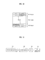
- FIG. 1 illustrates physical channels used in a 3GPP LTE system and a signal transmission method using the same
- FIG. 2 illustrates an uplink signal processing procedure
- FIG. 3 illustrates a downlink signal processing procedure
- FIG. 4 illustrates SC-FDMA and OFDMA schemes
- FIG. 5 illustrates a signal mapping scheme in a frequency domain, which satisfies single carrier property
- FIG. 6 illustrates a signal processing procedure of mapping DFT process output samples to a single carrier in clustered SC-FDMA
- FIGS. 7 and 8 illustrate a signal processing procedure of mapping DFT process output samples to multiple carriers in clustered SC-FDMA
- FIG. 9 illustrates a signal processing procedure in segmented SC-FDMA
- FIG. 10 illustrates an uplink subframe structure
- FIG. 11 illustrates a signal processing procedure for transmitting a reference signal (RS) on uplink
- FIG. 12 illustrates a demodulation reference signal (DMRS) structure for PUSCH
- FIGS. 13 and 14 illustrate slot level structures of PUCCH formats 1a and 1b
- FIGS. 15 and 16 illustrate slot level structures of PUCCH formats 2/2a/2b
- FIG. 17 illustrates ACK/NACK channelization for PUCCH formats 1a and 1b
- FIG. 18 illustrates channelization for a hybrid structure of PUCCH formats 1/1a/1b and 2/2a/2b in the same PRB;
- FIG. 19 illustrates PRB allocation for PUCCH transmission
- FIG. 20 illustrates a concept of management of downlink component carriers in a base station (BS).
- BS base station
- FIG. 21 illustrates a concept of management of uplink component carriers in a user equipment (UE).
- UE user equipment
- FIG. 22 illustrates a concept of management of multiple carriers by one MAC layer in a BS
- FIG. 23 illustrates a concept of management of multiple carriers by one MAC layer in a UE
- FIG. 24 illustrates a concept of management of multiple carriers by multiple MAC layers in a BS
- FIG. 25 illustrates a concept of management of multiple carriers by multiple MAC layers in a UE
- FIG. 26 illustrates a concept of management of multiple carriers by multiple MAC layers in a BS
- FIG. 27 illustrates a concept of management of multiple carriers by one or more MAC layers in a UE
- FIG. 28 illustrates asymmetrical carrier aggregation in which a plurality of DL CCs are linked to one UL CC;
- FIG. 29 illustrates signal transmission through a PUCCH according to an embodiment of the present invention
- FIGS. 30 and 31 illustrate a PUCCH format and a signal processing procedure for the same according to an embodiment of the present invention
- FIGS. 32 and 33 illustrate a PUCCH format having an increased RS multiplexing capacity and a signal processing procedure therefor according to an embodiment of the present invention.
- FIG. 34 illustrates a signal processing block for transmitting a PUCCH through multiple antennas according to an embodiment of the present invention
- FIG. 35 illustrates PUCCHs generated for respective antenna ports in the signal processing block shown in FIG. 34 ;
- FIGS. 36 and 37 illustrate a signal processing block for transmitting a PUCCH through multiple antennas according to another embodiment of the present invention
- FIG. 38 illustrates PUCCHs generated for respective antenna ports in the signal processing block shown in FIGS. 36 and 38 ;
- FIGS. 39 illustrates a signal processing block for transmitting a PUCCH through multiple antennas according to another embodiment of the present invention.
- FIG. 40 illustrates a signal processing block for transmitting a PUCCH through multiple antennas according to another embodiment of the present invention.
- FIGS. 41 to 44 illustrate PUCCH formats and signal processing procedures for the same according to an embodiment of the present invention
- FIGS. 45 to 52 illustrate PUCCH resource allocation according to embodiments of the present invention
- FIG. 53 illustrates a PUCCH format and a signal processing procedure for the same according to another embodiment of the present invention.
- FIGS. 54 to 65 illustrate PUCCH resource allocation according to other embodiments of the present invention.
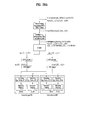
- FIG. 66 illustrates configurations of a BS and a UE applicable to the present invention.
- Embodiments of the present invention are applicable to a variety of wireless access technologies such as Code Division Multiple Access (CDMA), Frequency Division Multiple Access (FDMA), Time Division Multiple Access (TDMA), Orthogonal Frequency Division Multiple Access (OFDMA), Single Carrier Frequency Division Multiple Access (SC-FDMA), etc.
- CDMA can be implemented as a wireless technology such as Universal Terrestrial Radio Access (UTRA) or CDMA2000.
- TDMA can be implemented as a wireless technology such as Global System for Mobile communications (GSM)/General Packet Radio Service (GPRS)/Enhanced Data Rates for GSM Evolution (EDGE).
- GSM Global System for Mobile communications
- GPRS General Packet Radio Service
- EDGE Enhanced Data Rates for GSM Evolution
- OFDMA can be implemented as a wireless technology such as Institute of Electrical and Electronics Engineers (IEEE) 802.11 (Wireless Fidelity (Wi-Fi)), IEEE 802.16 (Worldwide interoperability for Microwave Access (WiMAX)), IEEE 802.20, Evolved UTRA (E-UTRA).
- UTRA is a part of Universal Mobile Telecommunications System (UMTS).
- 3GPP 3 rd Generation Partnership Project
- LTE Long Term Evolution
- E-UMTS Evolved UMTS
- LTE-A LTE-Advanced
- LTE-A is an evolution of 3GPP LTE. While the following description is given, centering on 3GPP LTE/LTE-A for clarity of description, this is purely exemplary and thus should not be construed as limiting the present invention.
- a UE receives information from a BS through downlink and transmits information to the BS through uplink.
- Information transmitted and received between the BS and the UE includes data and various types of control information.
- Various physical channels are present according to type/usage of information transmitted and received between the BS and the UE.
- FIG. 1 illustrates physical channels used in a 3GPP LTE system and a signal transmission method using the same.
- the UE When powered on or when a UE initially enters a cell, the UE performs initial cell search involving synchronization with a BS in step S101.
- the UE may be synchronized with the BS and acquire information such as a cell Identifier (ID) by receiving a Primary Synchronization Channel (P-SCH) and a Secondary Synchronization Channel (S-SCH) from the BS. Then the UE may receive broadcast information from the cell on a Physical Broadcast Channel (PBCH).
- P-SCH Primary Synchronization Channel
- S-SCH Secondary Synchronization Channel
- PBCH Physical Broadcast Channel
- the UE may determine a downlink channel status by receiving a Downlink Reference Signal (DL RS) during initial cell search.
- DL RS Downlink Reference Signal
- the UE may acquire more specific system information by receiving a Physical Downlink Control Channel (PDCCH) and receiving a Physical Downlink Shared Channel (PDSCH) based on information of the PDCCH in step S102.
- PDCCH Physical Downlink Control Channel
- PDSCH Physical Downlink Shared Channel
- the UE may perform a random access procedure to access the BS in steps S103 to S106.
- the UE may transmit a preamble to the BS on a Physical Random Access Channel (PRACH) (S103) and receive a response message for preamble on a PDCCH and a PDSCH corresponding to the PDCCH (S104).
- PRACH Physical Random Access Channel
- the UE may perform a contention resolution procedure by further transmitting the PRACH (S105) and receiving a PDCCH and a PDSCH corresponding to the PDCCH (S106).
- the UE may receive a PDCCH/PDSCH (S107) and transmit a Physical Uplink Shared Channel (PUSCH)/Physical Uplink Control Channel (PUCCH) (S108), as a general downlink/uplink signal transmission procedure.
- control information transmitted from the UE to the BS is called uplink control information (UCI).
- the UCI may include a Hybrid Automatic Repeat and request Acknowledgement/Negative-ACK (HARQ ACK/NACK) signal, scheduling request (SR), a Channel Quality Indicator (CQI), a Precoding Matrix Index (PMI), a Rank Indication (RI), etc.
- HARQ ACK/NACK Hybrid Automatic Repeat and request Acknowledgement/Negative-ACK
- SR scheduling request
- CQI Channel Quality Indicator
- PMI Precoding Matrix Index
- RI Rank Indication
- the UCI While the UCI is transmitted through a PUCCH in general, it may be transmitted through a PUSCH when control information and traffic data need to be simultaneously transmitted.
- the UCI may be aperiodically transmitted through a PUSCH at the request/instruction of a network.
- FIG. 2 illustrates a signal processing procedure through which a UE transmits an uplink signal.
- a scrambling module 210 of the UE may scramble the uplink signal using a UE-specific scrambling signal.
- the scrambled signal is input to a modulation mapper 220 in which the scrambled signal is modulated into complex symbols using Binary Phase Shift Keying (BPSK), Quadrature Phase Shift Keying (QPSK) or 16-Quadrature Amplitude Modulation (QAM)/64-QAM according to signal type and/or channel status.
- BPSK Binary Phase Shift Keying
- QPSK Quadrature Phase Shift Keying
- QAM 16-Quadrature Amplitude Modulation
- the modulated complex symbols are processed by a transform precoder 230, and then applied to a resource element mapper 240.
- the resource element mapper 240 may map the complex symbols to time-frequency resource elements.
- the signal processed in this manner may be subjected to an SC-FDMA signal generator 250 and transmitted to a BS through an antenna.
- FIG. 3 illustrates a signal processing procedure through which the BS transmits a downlink signal.
- the BS may transmit one or more codewords on downlink.
- the codewords may be processed into complex symbols through scrambling modules 301 and modulation mappers 302 as in the uplink shown in FIG. 2 .
- the complex symbols are mapped to a plurality of layers by a layer mapper 303.
- the layers may be multiplied by a precoding matrix in a precoding module 304 and allocated to each of transmit antennas.
- the processed signals for the respective antennas may be mapped to time-frequency resource elements by a resource element mapper 305 and subjected to an OFDM signal generator 306 to be transmitted through the antennas.
- uplink signal transmission uses SC-FDMA while downlink signal transmission uses OFDMA, as described above with reference to FIGS. 2 and 3 .
- FIG. 4 illustrates SC-FDMA and OFDMA schemes.
- the 3GPP system employs OFDMA scheme in downlink and employs SC-FDMA scheme in uplink.
- both a UE for transmitting an uplink signal and a BS for transmitting a downlink signal include a serial-to-parallel converter 401, a subcarrier mapper 403, an M-point IDFT module 404, and a cyclic prefix (CP) adder 406.
- the UE for transmitting a signal according to SC-FDMA additionally includes an N-point DFT module 402.
- FIG. 5 illustrates a signal mapping scheme in a frequency domain, which satisfies single carrier property.
- FIG. 5(a) illustrates a localized mapping scheme and
- FIG. 5(b) illustrates a distributed mapping scheme.
- Clustered SC-FDMA which is a modified version of SC-FDMA, will now be described.
- DFT process output samples are divided into sub-groups in a subcarrier mapping process and the sub-groups are discretely mapped to the frequency domain (or subcarrier domain).
- FIG. 6 illustrates a signal processing procedure for mapping DFT process output samples to a single carrier in clustered SC-FDMA.
- FIGS. 7 and 8 illustrate a signal processing procedure for mapping DFT process output samples to multiple carriers in clustered SC-FDMA.
- FIG. 6 shows an example of applying intra-carrier clustered SC-FDMA while FIGS. 7 and 8 show examples of applying inter-carrier clustered SC-FDMA.
- FIG. 7 illustrates a case in which a signal is generated through a single IFFT block when subcarrier spacing between neighboring component carriers is configured while component carriers are contiguously allocated in the frequency domain.
- FIG. 8 shows a case in which a signal is generated through a plurality of IFFT blocks when component carriers are non-contiguously allocated in the frequency domain.
- FIG. 9 illustrates a signal processing procedure in segmented SC-FDMA.
- Segmented SC-FDMA is a simple extension of the DFT spreading and IFFT subcarrier mapping structure of the conventional SC-FDMA, when the number of DFT blocks is equal to the number of IFFT blocks and thus the DFT blocks and the IFFT blocks are in one-to-one correspondence. While the term 'segmented SC-FDMA' is adopted herein, it may also be called NxSC-FDMA or NxDFT spread OFDMA (NxDFT-s-OFDMA).
- NxSC-FDMA NxDFT spread OFDMA
- NxDFT-s-OFDMA NxDFT spread OFDMA
- FIG. 10 illustrates an uplink subframe structure.
- an uplink subframe includes a plurality of slots (e.g. two slots).
- the slots may include different numbers of SC-FDMA symbols according to CP length.
- the slot can include 7 SC-FDMA symbols in case of normal CP.
- the uplink subframe is divided into a data region and a control region.
- the data region includes a PUSCH and is used to transmit a data signal such as voice data.
- the control region includes a PUCCH and is used to transmit UCI.
- the UCI includes HARQ ACK/NACK, CQI, PMI, RI, etc.
- FIG. 11 illustrates a signal processing procedure for transmitting a reference signal (RS) on uplink. While data is converted into a frequency domain signal through a DFT precoder, frequency-mapped, and then transmitted through IFFT, an RS does not passes the DFT precoder. Specifically, an RS sequence is generated directly in the frequency domain (S11) and then is sequentially subjected to localization mapping (S12), IFFT (S13) and CP addition (S14) to be transmitted.
- S12 localization mapping
- S13 IFFT
- S14 CP addition
- RS sequence r u , v ⁇ n is defined by a cyclic shift ⁇ of a base sequence and may be represented by Equation 1.
- r u , v ⁇ n e j ⁇ n ⁇ r u , v n , 0 ⁇ n ⁇ M sc RS
- M sc RS m ⁇ N sc RB is the length of the RS sequence
- N sc RB is a resource block size on a subcarrier basis
- UL represents a maximum uplink transmsision bandwidth.
- Base sequences r ⁇ u,v ( n ) are divided into several groups.
- u ⁇ 0,1,...,29 ⁇ denotes the group number and ⁇ corresponds to the base sequence number within the corresponding group.
- the sequence group number u and the base sequence number ⁇ within the corresponding group may vary with time.
- Base sequence r u , v 0 , ... , r u , v ⁇ M sc RS - 1 depends on the sequence length M sc RS .
- a base sequence of length 3 ⁇ N sc RB or larger can be defined as follows.
- the q-th root Zadoff-Chu sequence can be defined by the following Equation 3.
- x q m e - j ⁇ ⁇ qm ⁇ m + 1 M ZC RS , 0 ⁇ m ⁇ M ZC RS - 1
- N ZC RS of the Zadoff-Chue sequence is given by the largest prime numbersuch that N ZC RS ⁇ M sc RS is satisfied.
- a base sequence of length less than 3 ⁇ N sc RB can be defined as follows.
- r u , v n e j ⁇ n ⁇ ⁇ / 4 , 0 ⁇ n ⁇ M sc RS - 1
- the sequence group number u in slot n s can be defined by group hopping pattern f gh (n s ) and a sequence-shift pattern f ss according to Equation 6.
- u f gh n s + f ss ⁇ mod 30
- mod denotes a modulo operation
- Sequence group hopping may be enabled or disabled by means of a parameter that enables group hopping and is provided by higher layers.
- PUCCH and PUSCH have the same hopping pattern but may have different sequence-shift patterns.
- the group hopping pattern f gh (n s ) is the same for PUSCH and PUCCH and given by the following Equation 7.
- Sequence-shift f ss differs between PUCCH and PUSCH.
- sequence-shift pattern f ss PUCCH N ID cell mod 30.
- sequence shift pattern f ss PUSCH f ss PUCCH + ⁇ ss ⁇ mod 30. ⁇ ss ⁇ 0,1,...,29 ⁇ is configured by higher layers.
- Sequence hopping only applies for reference signals of length M sc RS ⁇ 6 ⁇ N sc RB .
- c(i) corresponds to the pseudo-random sequence and a parameter that is provided by higher layers and enables sequence hopping determines if sequence hopping is enabled or not.
- a reference signal for PUSCH is determined as follows.
- n DMRS 1 is a broadcast value
- n DMRS 2 is given by uplink scheduling allocation
- n PRS (n s ) is a cell-specific cyclic shift value.
- c(i) denotes the psedo-random sequence and is a cell-specific value.
- Table 3 shows a cyclic shift field and n DMRS 2 in downlink control information (DCI) format 0.
- DCI downlink control information
- the sequence is multiplied with the amplitude scaling factor ⁇ PUSCH and mapped to the same set of a physical resource block (PRB) used for the corresponding PUSCH in a sequence starting with r PUSH (0).
- PRB physical resource block
- a ZC sequence is used with cyclic extension for length 3 ⁇ N sc RB or larger, whereas a computer generated sequence is used for length less than 3 ⁇ N sc RB .
- a cyclic shift is determined according to cell-specific cyclic shift, UE-specific cyclic shift and hopping pattern.
- FIG. 12a shows a DMRS structure for PUSCH in case of normal CP and FIG. 12b shows a DMRS structure for PUSCH in case of extended CP.
- a DMRS is transmitted through the fourth and eleventh SC-FDMA symbols in FIG. 12a and transmitted through the third and ninth SC-FDMA symbols in FIG. 12b .
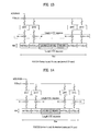
- FIGS. 13 to 16 illustrate slot level structures of PUCCH formats.
- a PUCCH has the following formats in order to transmit control information.
- Table 4 shows modulation schemes according to PUCCH format and the number of bits per subframe.
- Table 5 shows the number of RSs per slot according to PUCCH format and
- Table 6 shows SC-FDMA symbol position in an RS according to PUCCH format.
- PUCCH formats 2a and 2b correspond to normal CP.
- FIG. 13 illustrates PUCCH formats 1a and 1b in case of normal CP and FIG. 14 illustrates PUCCH formats 1a and 1b in case of extended CP.
- PUCCH formats 1a and 1b the same control information is repeated in a subframe on a slot-by-slot basis.
- ACK/NACK signals are respectively transmitted from UEs through different resources configured by different cyclic shifts (CSs) (frequency domain codes) and orthogonal cover codes (OCs or OCCs) (time domain spreading codes) of a computer-generated constant amplitude zero auto correlation (CG-CAZAC) sequence.
- CSs cyclic shifts
- OCCs orthogonal cover codes
- An OC includes a Walsh/DFT orthogonal code, for example.
- Orthogonal sequences w0,w1,w2,w3 may be applied in the arbitrary time domain (after FFT modulation) or in the arbitrary frequency domain (prior to FFT modulation).
- An ACK/NACK resource composed of CS, OC and PRB may be given to a UE through radio resource control (RRC) for SR and persistent scheduling.
- RRC radio resource control
- the ACK/NACK resource may be implicitly provided to the UE by the lowest CCE index of a PUCCH corresponding to a PDSCH for dynamic ACK/NACK and non-persistent scheduling.
- FIG. 15 illustrates PUCCH formats 2/2a/2b in case of normal CP
- FIG. 16 illustrates PUCCH formats 2/2a/2b in case of extended CP.
- one subframe includes 10 QPSK data symbols in addition to RS symbols in case of normal CP.
- Each of the QPSK symbols is spread in the frequency domain by CS and then mapped to the corresponding SC-FDMA symbol.
- SC-FDMA symbol level CS hopping may be applied to randomize inter-cell interference.
- An RS may be multiplexed by CDM using CSs. For example, if the number of available CSs is 12 or 6, 12 or 6 UEs can be multiplexed in the same PRB. That is, a plurality of UEs can be multiplexed by CS+OC+PRB and CS+PRB in PUCCH formats 1/1a/1b and 2/2a/2b respectively.
- Orthogonal sequences with length-4 and length-3 for PUCCH formats 1/1a/1b are shown in Table 7 and Table 8.
- Table 7 Length-4 orthogonal sequences for PUCCH formats 1/1a/1b
- Sequence index n oc (n s ) Orthogonal sequences ⁇ w 0 ⁇ w ⁇ N SF PUCCH - 1 0 [+1 +1 +1 +1] 1 [+1 -1 +1 -1] 2 [+1 -1 -1 +1]
- Sequence index n oc (n s ) Orthogonal sequences ⁇ w 0 ⁇ w ⁇ N SF PUCCH - 1 0 [1 1 1] 1 [1 e j2 ⁇ /3 e j4 ⁇ /3 ] 2 [1 e j4 ⁇ /3 e j2 ⁇ /3 ]
- FIG. 17 illustrates ACK/NACK channelization for PUCCH formats 1a and 1b.
- FIG. 18 illustrates channelization for a hybrid structure of PUCCH formats 1/1a/1b and 2/2a/2b in the same PRB.
- CS hopping and OC remapping may be applied as follows.
- Resource n r for PUCCH formats 1/1a/1b includes the following combination.
- a representative index n r includes n cs , n oc and n rb , where indexes indicating CS, OC and RB are n cs , n oc , and n rb , respectively.
- CQI, PMI, RI and a combination of CQI and ACK/NACK may be transmitted through PUCCH formats 2/2a/2b.
- RM Reed-Muller
- channel coding for a UL CQI in an LTE system is described as follows.
- Bit stream a 0 , a 1 , a 2 , ... a A-1 is channel-coded using RM code (20,A).
- Table 10 shows a base sequence for code (20,A).
- a 0 and a A-1 denote the most significant bit (MSB) and the least significant bit (LSB).
- MSB most significant bit
- LSB least significant bit
- a maximum number of information bits is 11 in cases other than a case in which CQI and ACK/NACK are simultaneously transmitted.
- the UL CQI may be subjected to QPSK modulation after being coded into 20 bits using the RM code.
- the coded bits may be scrambled before being subjcted to QPSK modulation.
- [Table 10] I M i,0 M i,1 M i,2 M i,3 M i,4 M i,5 M i,6 M i,7 M i,8 M i,9 M i,10 M i,1 1 M i,1 2 0 1 1 0 0 0 0 0 0 0 0 0 1 1 0 1 1 1 1 0 0 0 0 0 0 1 1 1 0 2 1 0 0 1 0 1 0 0 1 0 1 1 1 1 1 1 3 1 0 1 1 1 0 0 0 0 1 0 1 1 1 4 1 1 1 1 0 0 0 1 0 1 1 1 5 1 1 0 0 1 0 1 1 1 0 1 1 6 1 0 1 0 1 0 1 0 1 0 1 1 1 1 1 7 1 0 0 1 1 0 1
- Channel-coded bits b 0 , b 1 , b 2 , b 3 ,...,b B-1 may be generated by Equation 9.
- i 0, 1, 2, ..., B-1.
- Table 11 shows an uplink control information (UCI) field for wideband (single antenna port, transmit diversity or open loop spatial multiplexing PDSCH) CQI feedback.
- UCI uplink control information
- Table 11 Field Band Wideband CQI 4
- Table 12 shows a UCI field for wideband CQI and PMI feedback. This field reports closed loop spatial multiplexing PDSCH transmission.
- Table 13 shows a UCI field for RI feedback for wideband report. [Table 13] Field Bit widths 2 antenna ports 4 antenna ports Maximum 2 layers Maximum 4 layers RI (Rank Indication) 1 1 2
- FIG. 19 illustrates PRB allocation. As shown in FIG. 19 , a PRB may be used for PUCCH transmission in slot n s .
- a multi-carrier system or a carrier aggregation system means a system using aggregation of a plurality of carriers having a bandwidth narrower than a target bandwidth for supporting wideband.
- the bandwidth of the aggregated carriers may be limited to the bandwidths used in existing systems for backward compatibility with the existing systems.
- an LTE system supports bandwidths of 1.4MHz, 3MHz, 5MHz, 10MHz, 15MHz and 20MHz and an LTE-A system evolved from the LTE system can support bandwidths wider than 20MHz by using bandwidths supported by the LTE system.
- a new bandwidth may be defined to support carrier aggregation irrespective of the bandwidths used in existing systems.
- the term 'multi-carrier' can be used with carrier aggregation and bandwidth aggregation.
- Carrier aggregation collectively refers to both contiguous carrier aggregation and non-contiguous carrier aggregation.
- FIG. 20 illustrates a concept of management of downlink component carriers in a BS
- FIG. 21 illustrates a concept of management of uplink component carriers in a UE.
- higher layers are simply referred to as a MAC layer in the following description.
- FIG. 22 illustrates a concept of management of multiple carriers by one MAC layer in a BS
- FIG. 23 illustrates a concept of management of multiple carriers by MAC layer in a UE.
- one MAC layer manages and operates one or more frequency carriers for transmission and reception. In this case, resource management is flexible because frequency carriers managed by one MAC layer need not be contiguous.
- one PHY layer corresponds to one component carrier.
- one PHY layer does not necessarily mean an independent radio frequency (RF) device. While one independent RF device means one PHY layer in general, one RF device is not limited thereto and may include multiple PHY layers.
- RF radio frequency
- FIG. 24 illustrates a concept of management of multiple carriers by multiple MAC layers in a BS and FIG. 25 illustrates a concept of management of multiple carriers by multiple MAC layers in a UE.
- FIG. 26 illustrates a concept of management of multiple carriers by multiple MAC layers in a BS and
- FIG. 27 illustrates a concept of management of multiple carriers by one or more MAC layers in a UE.
- multiple carriers may be controlled by multiple MAC layers as shown in FIGS. 24 to 27 .
- Multiple MAC layers may control one-to-one multiple carriers as shown in FIGS. 24 and 25 .
- MAC layers may control one-to-one some carriers and one MAC layer may control other carriers.
- the above-described system includes one to N carriers which are contiguous or non-contiguous. This can be applied in both uplink and downlink.
- a TDD system is configured such that N carriers for downlink transmission and uplink transmission are operated and an FDD system is configured such that multiple carriers are respectively used for uplink and downlink.
- the FDD system may support asymmetrical carrier aggregation in which the numbers of aggregated carriers and/or carrier bandwidths are different between uplink and downlink.
- FIG. 28 illustrates a scenario of transmitting uplink control information (UCI) in a wireless communication system that supports carrier aggregation.
- UCI uplink control information
- This scenario is based on the assumption that UCI is ACK/NACK (A/N) information.
- UCI can include control information such as channel status information (e.g. CQI, PMI, RI, etc.) and scheduling request information (e.g. SR).
- channel status information e.g. CQI, PMI, RI, etc.
- SR scheduling request information
- FIG. 28 illustrates asymmetrical carrier aggregation in which 5 DL CCs are linked to one UL CC.
- This asymmetrical carrier aggregation may be configured from the viewpoint of UCI transmission. That is, DL CC-UL CC linkage for the UCI and DL CC-UL CC linkage for data may be different from each other.
- DL CC-UL CC linkage for the UCI and DL CC-UL CC linkage for data may be different from each other.
- at least two UL ACK/NACK bits are needed. In this case, for data received through 5 DL CCs, at least 10 ACK/NACK bits are needed to transmit ACK/NACK information through one UL CC.
- the conventional PUCCH formats 1a/1b can transmit ACK/NACK information having a maximum of 2 bits, and thus it cannot transmit ACK/NACK information having an increased number of bits. While it has been described that carrier aggregation increases the quantity of UCI, an increase in the number of antennas, presence of a backhaul subframe in a TDD system and a relay system, etc. may cause an increase in the quantity of UCI.
- a DL CC and a UL CC may also be respectively referred to as a DL cell and a UL cell and an anchor DL CC.
- an anchor UL CC may be respectively referred to as a DL primary cell (PCell) and a UL PCell.
- the DL primary CC may be defined as a DL CC linked with the UL primary CC.
- linkage includes both implicit linkage and explicit linkage.
- one DL CC and one UL CC are uniquely paired.
- a DL CC linked with the UL primary CC according to LTE paring can be called the DL primary CC.
- This can be regarded as implicit linkage.
- Explicit linkage means that a network configures a linkage in advance and it may be signaled through RRC.
- a DL CC paired with the UL primary CC may be called the DL primary CC.
- the UL primary (anchor) CC may be a UL CC that carries a PUCCH.
- the UL primary CC may be a UL CC that carries UCI over a PUCCH or a PUSCH.
- the DL primary CC can be configured through higher layer signaling.
- the DL primary CC may be a DL CC through which a UE performs initial access.
- DL CCs other than the DL primary CC can be called DL secondary CCs.
- UL CCs other than the UL primary CC can be called UL secondary CCs.
- DL-UL pairing may be applied to FDD only.
- DL-UL pairing may not be additionally defined for TDD because TDD uses the same frequency.
- DL-UL linkage may be determined from UL linkage through UL EARFCN information of SIB2.
- SIB2 linkage can be obtained through SIB2 decoding in the event of initial access and acquired through RRC signaling in other cases. Accordingly, there is only SIB2 linkage and other DL-UL pairing may not be explicitly defined. For example, in a 5DL:1UL structure shown in FIG.
- DL CC#0 and UL CC#0 is in a SIB2 linkage relationship with each other and other DL CCs may be in a SIB2 linkage relationship with other UL CCs that are not configured for the corresponding UE.
- While some embodiments are focused on asymmetrical carrier aggregation, the present invention can be applied to various carrier aggregation scenarios including symmetrical carrier aggregation.
- the PUCCH format proposed by the present invention is referred to as a new PUCCH format, LTE-A PUCCH format, or PUCCH format 3 in view of the fact that up to PUCCH format 2 has been defined in LTE.
- the following description is focused on a case in which multiple ACK/NACK bits are used as an example of an increased quantity of control information.
- the control information is not limited to multiple ACK/NACK bits in the present invention.
- New PUCCH formats and transmission schemes may include the following.
- the present invention can further include other PUCCH formats other than the following examples.
- FIG. 29 illustrates signal transmission using the new PUCCH format.
- one DL primary component carrier (DL PCC) and one DL secondary component carrier (DL SCC) are present.
- the DL PCC may be linked with a UL PCC. It is assumed that there is one DL grant in each of the DL PCC and the DL SCC and a PDCCH is transmitted through each CC. If each DL CC transmits 2 codewords (a total of 4 codewords), it is possible to transmit 4 bits when a DTX status is not reported and 5 bits when the DTX status is reported over the UL PCC through the new PUCCH format.
- the UCI/RS symbol structure of the existing PUCCH format 1 (normal CP) of LTE is used as a subframe/slot based UCI/RS symbol structure applied to a PUCCH format according to an embodiment of the present invention.
- the subframe/slot based UCI/RS symbol structure is exemplary and the present invention is not limited to a specific UCI/RS symbol structure.
- the number of UCI/RS symbols, positions of the UCI/RS symbols, etc. may be freely changed according to system designs.
- the PUCCH format according to the present invention can be defined using the RS symbol structures of the existing PUCCH format 2/2a/2b of LTE.
- the PUCCH format according to embodiments of the present invention can be used to transmit arbitrary types/sizes of UCI.
- the PUCCH format 3 according to the present invention can transmit information such as HARQ ACK/NACK, CQI, PMI, RS, SR, etc. This information may have a payload of an arbitrary size. Description of the following embodiments and drawings are focused on a case in which the PUCCH format according to the present invention transmits ACK/NACK information.
- FIGS. 30a to 30f illustrate structures of a PUCCH format 3 and signal processing procedures for the same according to an embodiment of the present invention.
- FIG. 30a illustrates a case in which PUCCH format 3 according to the present invention is applied to PUCCH format 1 (normal CP).
- a channel coding block performs channel coding for information bits a_0, a_1, ..., a_M-1 (e.g. multiple ACK/NACK bits) to generate encoded bits (coded bits or coding bits) (or a codeword) b_0, b_1, ..., b_N-1.
- M denotes an information bit size
- N denotes an encoded bit size.
- the information bits include multiple ACK/NACK bits for a plurality of data (or PDSCH) received through a plurality of DL CCs, for example.
- the information bits a_0, a_1, ..., a_M-1 are joint-coded regardless of the type/number/size of UCI that forms the information bits.
- channel coding is not limited thereto and includes simple repetition, simplex coding, Reed Muller (RM) coding, punctured RM coding, Tail-biting convolutional coding (TBCC), low-density parity-check (LDPC) or turbo-coding.
- the encoded bits can be rate-matched in consideration of a modulation order and resource quantity, which is not shown in the figure.
- the rate matching function may be included as a part of the channel coding block or may be executed by a separate functional block.
- a modulator modulates the encoded bits b_0, b_1, ..., b_N-1 to generate modulation symbols c_0, c_1, ..., c_L-1 where L denotes the size of the modulation symbols.
- a modulation method is performed by modifying the size and phase of a transmission signal.
- the modulation method includes n-PSK (Phase Shift Keying) and n-QAM (Quadrature Amplitude Modulation) (n being an integer of 2 or greater).
- the modulation method may include BPSK (Binary PSK), QPSK (Quadrature PSK), 8-PSK, QAM, 16-QAM, 64-QAM, etc.
- a divider divides the modulation symbols c_0, c_1, ..., c_L-1 into slots.
- the order/pattern/scheme of dividing the modulation symbols into slots are not particularly limited.
- the divider can sequentially divide the modulation symbols into the slots (localized scheme).
- modulation symbols c_0, c_1, ..., c_L/2-1 can be divided into slot 0 and modulation symbols c_L/2, c_L/2+1, ..., c_L-1 can be divided into slot 1, as shown in FIG. 30a .
- the modulation symbols may be interleaved (or permuted) when divided into the slots. For example, even-numbered modulation symbols can be divided into slot 0 and odd-numbered modulation symbols can be divided into slot 1.
- the orders of the modulation operation and division operation may be changed with each other.
- a DFT precoder performs DFT precoding (e.g. 12-point DFT) for the modulation symbols divided into each slot in order to generate a single carrier waveform.
- DFT precoding e.g. 12-point DFT
- the modulation symbols c_0, c_1, ..., c_L/2-1 divided into slot 0 can be DFT-precoded into DFT symbols d_0, d_1, ..., d_L/2-1 and the modulation symbols c_L/2, c_L/2+1, ..., c_L-1 divided into slot 1 can be DFT-precoded into DFT symbols d_L/2, d_L/2+1, ..., d_L-1.
- DFT precoding can be replaced by other corresponding linear operations (e.g. Walsh precoding).
- a spreading block spreads the DFT precoded signal at an SC-FDMA symbol level (time domain).
- Time domain spreading at an SC-FDMA symbol level is performed using a spreading code (sequence).
- the spreading code includes a quasi-orthogonal code and an orthogonal code.
- the quasi-orthogonal code includes a pseudo noise (PN) code.
- PN pseudo noise
- the orthogonal code includes a Walsh code and a DFT code.
- the orthogonal code is not limited thereto.
- the orthogonal code is used as the spreading code for ease of description.
- the orthogonal code is exemplary and can be replaced by the quasi-orthogonal code.
- the maximum value of spreading code size is limited by the number of SC-FDMA symbols used for control information transmission. For example, when 4 SC-FDMA symbols are used for control information transmission in one slot, a (quasi) orthogonal code w0,w1,w2,w3 having a length of 4 can be used for each slot.
- the SF means a spreading degree of control information and may be related to a UE multiplexing order or an antenna multiplexing order.
- the signal generated through the above-mentioned procedure is mapped to subcarriers in a PRB and then subjected to IFFT to be transformed into a time domain signal.
- a cyclic prefix is added to the time domain signal to generate SC-FDMA symbols which are then transmitted through an RF unit.
- ACK/NACK bits for the DL CC may be 12 bits if a DTX status is included.
- Encoded bits are modulated into 24 QPSK symbols and 12 QPSK symbols are divided into each slot.
- 12 QPSK symbols are converted to 12 DFT symbols through 12-point DFT.
- the signal mapped to the PRB in the procedure shown in FIG. 30a may be obtained through various equivalent signal processing procedures. Signal processing procedures equivalent to the signal processing procedure of FIG. 30a will now be described with reference to FIGS. 30b to 30g .
- FIG. 30b shows a case in which the order of operations of the DFT precoder and the spreading block of FIG. 30a is changed with each other.
- the function of the spreading block corresponds to operation of multiplying a DFT symbol stream output from the DFT precoder by a specific constant at the SC-FMDA symbol level, and thus the same signal value is mapped to SC-FDMA symbols even though the order of operations of the DFT precoder and the spreading block is changed.
- the signal processing procedure for the PUCCH format 3 can be performed in the order of channel coding, modulation, division, spreading and DFT precoding.
- the division and spreading may be performed by one functional block. For example, modulation symbols can be alternately divided into slots and, simultaneously, spread at the SC-FDMA symbol level.
- the modulation symbols can be copied such that they correspond to the size of a spreading code when divided into the slots, and the copied modulation symbols can be multiplied one-to-one by respective elements of the spreading code. Accordingly, a modulation symbol stream generated for each slot is spread to a plurality of SC-FDMA symbols. Then, a complex symbol stream corresponding to the SC-FDMA symbols is DFT-precoded for each SC-FDMA symbol.
- FIG. 30c shows a case in which the order of operations of the modulator and the divider of FIG. 30a is changed.
- the signal processing procedure for PUCCH format 3 joint channel coding and division are performed at the subframe level, and modulation, DFT precoding and spreading are sequentially performed at the slot level.
- FIG. 30d shows a case in which the order of operations of the DFT precoder and the spreading block of FIG. 30c is changed.
- the function of the spreading block corresponds to operation of multiplying a DFT symbol stream output from the DFT precoder by a specific constant at the SC-FMDA symbol level, the same signal value is mapped to SC-FDMA symbols even though the order of operations of the DFT precoder and the spreading block is changed. Accordingly, in the signal processing procedure for PUCCH format 3, joint channel coding and division are performed at the subframe level, and modulation is carried out at the slot level. The modulation symbol stream generated for each slot is spread to a plurality of SC-FDMA symbols and DFT-precoded for each SC-FDMA symbol.
- the modulation and spreading operations can be performed by one functional block.
- the generated modulation symbols can be directly spread at the SC-FDMA symbol level during modulation of the encoded bits.
- the generated modulation symbols can be copied such that they correspond to the size of the spreading code and multiplied one-to-one by respective elements of the spreading code.
- FIG. 30e shows a case in which PUCCH format 3 according to the present embodiment is applied to PUCCH format 2 (normal CP) and
- FIG. 30f shows a case in which PUCCH format 3 according to the present embodiment is applied to PUCCH format 2 (extended CP). While a basic signal processing procedure is the same as the procedures described with reference to FIGS. 30a to 30d , the numbers/positions of UCI SC-FDMA symbols and RS SC-FDMA symbols are different from those of FIG. 30a since PUCCH format 2 of LTE is reused.
- Table 14 shows RS SC-FDMA symbol position in the PUCCH format 3. It is assumed that the number of SC-FDMA symbols in a slot is 7 (indexes: 0 to 6) in case of normal CP and 6 (indexes: 0 to 5) in case of extended CP. [Table 14] RS SC-FDMA symbol position Note PUCCH format 3 Normal CP Extended CP 2, 3, 4 2, 3 Reuse PUCCH format 1 1, 5 3 Reuse PUCCH format 2
- Tables 15 and 16 show exemplary spreading codes according to SF value.
- Code index m may be designated in advance or signaled from the BS.
- the code index m can be implicitly linked with an index (e.g. the lowest CCE index) of CCE constituting a PDCCH.
- the code index m may be explicitly designated through a PDCCH or RRC signaling.
- the code index m may be derived from a value designated through the PDCCH or RRC signaling.
- the code index m may be independently given for each subframe, each slot, and multiple SC-FDMA symbols.
- the code index m can be changed for each subframe, each slot and multiple SC-FDMA symbols. That is, the code index m can be hopped for each predetermined time interval.
- Cell-specific scrambling using a scrambling code e.g. a PN code such as a Gold code
- PCI physical cell ID
- UE-specific scrambling using a scrambling code corresponding to a UE ID e.g. RNTI
- Scrambling may be performed for the entire information, performed in SC-FDMA symbols, carried out between SC-FDMA symbols, or carried out for both the entire information and SC-FDMA symbols. Scrambling the entire information can be achieved by performing scrambling at the information bit level, encoded bit level and modulation symbol level prior to division.
- Intra-SC-FMDA symbol scrambling may be implemented by performing scrambling at the modulation symbol level or DFT symbol level after division.
- Inter-SC-FDMA symbol scrambling may be achieved by carrying out scrambling at the SC-FDMA symbol level in the time domain after spreading.
- UE multiplexing can be achieved by applying CDM before being subjected to the DFT precoder.
- the signal before being subjected to the DFT precoder is a time domain signal, and thus CDM can be implemented through circular shift (or cyclic shift) or Walsh (or DFT) spreading.
- An example of spreading Control information of each UE using Walsh code [+1 +1] [+1 -1] is as follows.
- interleaving may be additionally performed.
- the interleaving may be applied before or after spreading.
- An example of applying both the spreading and interleaving is as follows.
- - UE#1 [+1 -1] is applied.
- a 0 , ⁇ a 0 , a 1 , ⁇ a 1 , a 2 , ⁇ a 2 , a 3 , ⁇ a 3 , a 4 , ⁇ a 4 , a 5 , ⁇ a 5 are transmitted.
- a signal generated from spreading and/or interleaving in a stage prior to the DFT precoder is subjected to DFT precoding (and additionally subjected to time spreading at the SC-FDMA symbol level as necessary) and mapped to subcarriers of the corresponding SC-FDMA symbols.
- FIG. 31 illustrates another exemplary PUCCH format 3 according to the present invention. While PUCCH format 3 shown in FIG. 31 has the same basic structure as that of the PUCCH format shown in FIG. 30 , PUCCH format of FIG. 31 is different from PUCCH format 3 of FIG. 30 in that the same encoded bits are repeated on a slot-by-slot basis. Accordingly, a signal processing block shown in FIG. 31 does not include a divider.
- the multiplexing capacity of the RS is determined by a circular shift spacing ⁇ shift PUCCH .
- the multiplexing capacity of the RS is given by 12 ⁇ shift PUCCH .
- FIG. 32 illustrates an exemplary PUCCH structure having an increased multiplexing capacity.
- SC-FDMA symbol level spreading is applied to a symbol in the RS, and thus the multiplexing capacity of the RS is doubled.
- the orthogonal code cover is not limited thereto.
- y1 is applied to the first RS SC-FDMA symbol in a slot and y2 is applied to the second RS SC-FDMA symbol in the slot.
- FIG. 33 illustrates another exemplary PUCCH structure having an increased multiplexing capacity.
- the multiplexing capacity is further doubled by additionally performing slot-based spreading or covering (e.g. Walsh covering).
- slot-based Walsh covering is applied when slot-level frequency hopping is performed, orthogonality may be damaged due to a channel condition difference between slots.
- the slot-based spreading code is not limited thereto.
- x1 is applied to the first slot and x2 is applied to the second slot.
- FIG. 33 illustrates that slot level spreading (covering) is performed, and then SC-FDMA symbol level spreading (or covering) is carried out, the order of the operations may be changed.
- the increased multiplexing capacity of the RS may be used for channel estimation for each antenna (port) for transmit diversity (TxD) transmission.
- the multiplexing capacity of the RS can be increased using the aforementioned method.
- the scheme of increasing the RS multiplexing capacity using a spreading code e.g. Walsh cover
- the Walsh cover may be applied to RS symbols in TxD mode and may not be applied to RS symbols in non-TxD mode (which is equivalent to application of [+1 +1]).
- a spatial multiplexing gain can be obtained using one orthogonal resource (i.e. the same PRB and orthogonal code).
- the same orthogonal code can be applied to UCI symbols of antenna (port) 0 and antenna (port) 1 and different orthogonal cover codes (e.g. Walsh codes) can be applied to RS symbols of antenna (port) 0 and antenna (port) 1 in a 2TxD mode.
- a TxD mode may be configured through higher layer signaling (e.g. RRC signaling, MAC signaling, etc.) or physical layer signaling (e.g. PDCCH).
- TxD transmission schemes include spatial orthogonal resource transmit diversity (SORTD), space frequency block coding (SFBC), space time block coding (STBC) and frequency-switched transmit diversity (FSTD).
- SORTD spatial orthogonal resource transmit diversity
- SFBC space frequency block coding
- STBC space time block coding
- FSTD frequency-switched transmit diversity
- the TxD transmission schemes are not limited thereto.
- 2Tx transmit diversity scheme according to SORTD is described in the following embodiment. However, the embodiment can be equally/similarly expanded to an n-Tx transmit diversity scheme. It is assumed that a (quasi) orthogonal resource for control information transmission is referred to as resource A and a (quasi) orthogonal resource for RS transmission is referred to as resource B. Logical indexes of resource A and resource B may be linked with each other. For example, if the logical index of resource B is given, the logical index of resource A can be automatically determined. The logical indexes of resource A and resource B may be configured through different physical configuration methods. The following two cases are present.
- Control information can be transmitted through the same PRB at all antennas (ports).
- the control information can be transmitted through two different resources A (e.g. an orthogonal code, a subcarrier shift (or offset or index) according to frequency factor, or combinations thereof).
- the orthogonal code includes a Walsh code and a DFT code and the frequency factor can be given by N sc /N freq or the reciprocal thereof.
- N sc denotes the number of subcarriers in a PRB
- N freq denotes the number of subcarriers used for control information transmission.
- An RS can be transmitted through two different resources B (e.g. a combination of a circular shift and a DFT cover) selected for each antenna (port).
- two different resources B e.g. a combination of a circular shift and a DFT cover
- the control information can be transmitted through different PRBs for antennas.
- the control information can be transmitted through PRB#4 at antenna (port) 0 and transmitted through PRB#6 at antenna (port) 1.
- Resources for the control information transmitted through different antennas (ports) are not particularly limited (i.e. the resources can be equal to and different from each other).
- Resources for RSs transmitted through different antennas (ports) are not particularly limited (i.e. the resources can be equal to and different from each other).
- two resources A for control information transmission and two resources B for RS transmission can be defined in advance or provided through physical control channel (e.g. PDCCH) or RRC signaling.
- PDCCH physical control channel
- RRC Radio Resource Control
- signaling for the control information and RS can be individually performed.
- resource information for one antenna (port) is signaled
- resource information for the other antenna (port) can be inferred from the previously signaled resource information.
- code index m and/or the subcarrier position e.g. shift, offset or index
- code index m and/or the subcarrier position e.g.
- code index m and/or the subcarrier position (e.g. shift, offset or index) according to frequency factor can be explicitly designated through PDCCH or RRC signaling.
- the code index m and/or the subcarrier position (e.g. shift, offset or index) according to frequency factor can be changed on a subframe, slot or multi-SC-FDMA symbol basis. That is, the code index m and/or the subcarrier position (e.g. shift, offset or index) according to frequency factor can be hopped in the unit of a specific time interval (e.g. slot).
- FIG. 34 illustrates an exemplary signal processing block/procedure for SORTD.
- a basic process in the signal processing procedure other than a process for multi-antenna transmission, corresponds to that described with reference to FIGS. 30 to 33 .
- modulation symbols c_0, ⁇ ,c_23 are DFT-precoded and then transmitted through resources (e.g. an OC, a PRB or a combination thereof) assigned for each antenna port. While DFT operation is performed once for a plurality of antenna ports in the present embodiment, the DFT operation may be carried out for each antenna port.
- a modified form e.g. a complex conjugate form or scaled form
- a modified form e.g. a complex conjugate form or scaled form
- Equation 10 represents a process of DFT-precoding the modulation symbols on the assumption that the number of modulation symbols is 24 and 12 modulation symbols are divided into each slot.
- d () denotes a DFT-precoded modulation symbol stream
- c () denotes a modulation symbol stream
- N sc represents the number of subcarriers in a PRB.
- Equation 11 represents a process of spreading the DFT-precoded modulation symbol stream such that the modulation symbol stream corresponds to a plurality of SC-FDMA symbols in a PUCCH.
- z() denotes a spread modulation symbol stream corresponding to SC-FDMA symbols for the control information
- p denotes an antenna port
- w oc0 represents an orthogonal code applied to slot
- w oc1 represents an orthogonal code applied to slot 1
- 1 is a value in the range of 0 to (the number of SC-FDMA symbols for the control information in slot 0)-1
- m is a value in the range of 0 to (the number of SC-FDMA symbols for the control information in slot 1)-1.
- z (0) () is transmitted in PRB (0) through antenna port 0 and z (1) () is transmitted in PRB (1) through antenna port 1.
- [woc (0) ⁇ woc (1) ; PRB (0) ⁇ FPRB (1) ] is possible.
- Equation 12 represents a process of spreading the modulation symbol stream such that the modulation symbol stream corresponds to a plurality of SC-FDMA symbols in a PUCCH.
- y() denotes a modulation symbol stream spread such that the modulation symbol stream corresponds to a plurality of SC-FDMA symbols in a slot of the PUCCH
- p denotes an antenna port
- c() denotes a modulation symbol stream
- w oc0 represents an orthogonal code applied to slot
- w oc1 represents an orthogonal code applied to slot 1
- 1 is a value in the range of 0 to (the number N SF,0 of SC-FDMA symbols for the control information in slot 0)-1
- m is a value in the range of 0 to (the number N SF,1 of SC-FDMA symbols for the control information in slot 1)-1.
- Equation 13 represents a process of DFT-precoding the spread modulation symbols.
- d () denotes a DFT-precoded modulation symbol stream
- y () denotes a modulation symbol stream which has been spread to correspond to the SC-FDMA symbols for the control information
- p represents an antenna port
- N SC represents the number of subcarriers in a PRB
- N SF represents the number of SC-FDMA symbols for the control information in a subframe.
- d (0) () is transmitted in PRB (0) through antenna port 0 and d (1) () is transmitted in PRB (1) through antenna port 1.
- PRB (0) PRB (1)
- woc (0) woc (1) ; PRB (0) ⁇ PRB (1)
- [woc (0) ⁇ woc (1) ; PRB (0) ⁇ PRB (1) ] is possible.
- FIGS. 35a and 35b respectively illustrate PUCCH structures for antenna (port) 0 and antenna (port) 1 when SORTD is applied according to the signal processing procedure.
- different PUCCH transmission resources e.g. combinations of orthogonal codes and PRBs
- antennas (ports) e.g. resource#0 for antenna 0 and resource#1 for antenna 1).
- Signals transmitted through antenna (port) 0 and antenna (port) 1 may be equal to each other or may have forms modified according to a predetermined rule.
- FIG. 36 illustrates another exemplary signal processing block/procedure for SORTD.
- This signal processing block/procedure joint-codes the control information and then distributes and maps the coded control information to multiple resources to obtain a spatial coding gain.
- 48 coding bits are generated, modulated according to QPSK, and then mapped to 24 subcarriers across 2 slots.
- a basic procedure in the signal processing procedure of FIG. 36 corresponds to that described with reference to FIGS. 30 to 33 .
- modulation symbols c_0, ⁇ ,c_47 are divided into each antenna port.
- modulation symbols c_0, ⁇ ,c_23 can be divided into antenna port 0 and modulation symbols c_24, ⁇ ,c_47 can be divided into antenna port 1.
- the modulation symbols may be interleaved (or permuted) when divided to the antenna ports.
- even-numbered modulation symbols can be divided into antenna port 0 whereas odd-numbered modulation symbols can be divided into antenna port 1.
- the modulation symbol stream is DFT-precoded for each antenna port, and then transmitted using a resource (e.g. an OCC (or OC), a PRB, or a combination thereof) assigned to each antenna port.
- a resource e.g. an OCC (or OC), a PRB, or a combination thereof
- the signal processing block/procedure of FIG. 36 is applicable to a QPSK modulation symbol interleaving pattern.
- the signal processing block/procedure of FIG. 36 can be applied to an interleaving pattern such as c_0,c_2, ⁇ ,c_46 (for orthogonal resource0) and c_1,c_3, ⁇ ,c47 (for orthogonal resource1).
- FIG. 37 illustrates a modified form of the signal processing block/procedure of FIG. 36 .
- a basic process of the signal processing procedure of FIG. 37 corresponds to that described with reference to FIGS. 30 to 33 and FIG. 36 .
- FIG. 38a illustrates a PUCCH structure for antenna port 0
- FIG. 38b illustrates a PUCCH structure for antenna port 1. Referring to FIGS. 38a and 38b , a signal for antenna port 0 is transmitted through PRB#0 whereas a signal for antenna port 1 is transmitted through PRB#1.
- a spreading code (or orthogonal cover code (OCC) or OC) for the control information and a circular shift or spreading code (or OCC or OC) for the RS at antenna port 0 antenna port 1 may be equal to each other.
- the multiplexing order of the RS corresponds to more than twice the multiplexing order of the control information
- the following 2Tx transmit diversity scheme can be applied.
- two from among resources CS+OC+PRB for the RS may be used for channel estimation of each of 2 transmit antennas (ports) and only one resource (subcarrier position+OC+PRB) may be used for the control information.
- the multiplexing order of the RS can be increased using the aforementioned method.
- the scheme of increasing the RS multiplexing capacity using a spreading code e.g. Walsh cover
- the Walsh cover may be applied to RS symbols in a TxD mode and may not be applied to the RS symbols in a non-TxD mode (which is equivalent to application of [+1 +1]).
- a spatial multiplexing gain can be obtained using one orthogonal resource (i.e. the same PRB and orthogonal code).
- the same orthogonal code can be applied to UCI symbols of antenna (port) 0 and antenna (port) 1 and different orthogonal cover codes (e.g. Walsh codes) can be applied to RS symbols of antenna (port) 0 and antenna (port) 1 in a 2TxD mode.
- FIG. 39a illustrates a signal processing procedure for transmitting the control information through multiple antennas according to an embodiment of the present invention
- FIGS. 39b and 39c respectively show extended forms of the PUCCH structures of antenna port 0 and antenna port 1.
- a basic process of the signal processing procedure of FIG. 39 is similar to that described with reference to FIGS. 30 to 33 .
- a TxD mapper distributes a DFT precoder output value to multiple antennas.
- the TxD mapper performs a resource allocation/MIMO (Multiple Input Multiple Output) precoding/process to transmit the control information through multiple antenna (ports).
- the function of the TxD mapper is not limited thereto.
- the TxD mapper can apply an Alamouti scheme to the DFT precoder output value in the frequency domain.
- the Alamouti scheme can be represented by the following matrix. s 1 - s 2 * s 2 s 1 *
- column 0 and column 1 respectively denote signal vectors transmitted through antenna (port) 0 and antenna (port) 1
- row 0 and row 1 respectively denote complex signal vectors transmitted through first and second subcarriers
- * represents complex conjugate operation. Any form linearly transformed from the matrix can be applied to the present invention.
- the order of DFT symbols mapped to SC-FDMA symbols corresponding to antenna (port) 1 is changed for every two DFT symbols.
- d_0, d_1, d_2, d_3 are mapped to the SC-FDMA symbols corresponding to antenna (port) 0
- -d_1*, d_0*, -d_3*, d_2* are mapped to the SC-FDMA symbols corresponding to antenna (port) 1.
- the present invention proposes a multi-antenna coding scheme that does not cause CM increase even when the Alamouti scheme is applied.
- the control information is mapped to antenna (port) 0
- the complex signal is mapped to subcarriers after being subjected to DFT precoding.
- the control information is mapped to antenna (port) 1
- (1) mapping to subcarriers in SC-FDMA symbols in reverse order, (2) complex conjugate operation and (3) alternate addition of minus sign are performed.
- Operations (1), (2) and (3) are exemplary and the order of the operations can be changed. This scheme can be equally applied to the embodiments of the present invention. For example, referring to FIG.
- a complex symbol stream mapped to SC-FDMA symbols transmitted through a first antenna (port) and a second antenna (port) can be given as follows.
- First antenna port a k
- Second antenna port - 1 mod k 2 ⁇ conj ⁇ a 11 - k
- a k denotes the complex symbol stream mapped to subcarriers of the SC-FDMA symbols
- k denotes a complex symbol index (0 to 11)
- mod (a, b) represents the remainder obtained when a is divided by b
- conj(a) represents the complex conjugate value of a.
- Equation 15 assumes a case in which the complex signal is mapped to all subcarriers in the SC-FDMA symbols. Equation 15 can be normalized to Equation 16 considering a case in which the complex signal is mapped to only part of the subcarriers in the SC-FDMA symbols.
- First antenna port a k
- Second antenna port - 1 mod k 2 ⁇ conj ⁇ a n - k or - 1 mod ⁇ k + 1 , 2 ⁇ conj ⁇ a n - k
- n (length of complex symbol stream a k mapped to the subcarriers of the SC-FDMA symbols)-1 (e.g. 0 ⁇ n ⁇ 11).
- the complex symbol stream mapped to the SC-FDMA symbols transmitted through the first antenna (port) or the second antenna (port) can be circular-shifted (e.g. shifted by half the length of the complex symbol stream) in the frequency domain.
- Tables 17, 18 and 19 show cases in which the Alamouti scheme is applied according to the embodiment of the present invention.
- orthogonal codes e.g. DFT codes
- FIG. 40a illustrates a signal processing block/procedure for STBC.
- space block coding is applied to contiguous virtual subcarriers before being subjected to DFT precoding.
- Alamouti coding is applied to a time domain sequence [a 0 , a 1 , a 2 , a 3 , ⁇ ,a 10 , a 11 ] T before being subjected to DFT precoding.
- the time domain sequence [a 0 , a 1 , a 2 , a 3 , ⁇ , a 10 , a 11 ] T includes a modulation sequence and is mapped to contiguous subcarriers of SC-FDMA symbols after spreading and DFT precoding.
- the Alamouti scheme can be represented by the following matrix. s 1 - s 2 * s 2 s 1 *
- column 0 and column 1 respectively represent signal vectors transmitted through antenna (port) 0 and antenna (port) 1 and row 0 and row 1 respectively denote the first and second elements which form the time domain sequence before being subjected to DFT precoding.
- * represents a complex conjugate operation. Any linear transformation of the above matrix is applicable to the present invention.
- a spatial multiplexing gain can be obtained using one orthogonal resource.
- an OCC can be applied to RS symbols transmitted through each antenna (port) in the time domain. That is, the same orthogonal code [w u (5) (0) w u (5) (1) w u (5) (2) w u (5) (3) w u (5) (4)] can be applied to UCI symbols of antenna (port) 0 and antenna (port) 1.
- w u (a) (b) denotes a code index
- a denotes the length of the orthogonal code
- b denotes an element number in the orthogonal code.
- different orthogonal code covers (e.g.
- Walsh codes can be applied to RS symbols of antenna (port) 0 and antenna (port) 1. For example, [+1 +1] can be applied to RS symbols corresponding to antenna (port) 0 and [+1 -1] can be applied to RS symbols corresponding to antenna (port) 1.
- FIG. 40b illustrates a signal processing block/procedure for FSTD.
- a basic process of this signal processing procedure other than a process for multi-antenna transmission, is identical to that described with reference to FIGS. 30 to 33 .
- the control information is sequentially subjected to channel encoding, scrambling and modulation.
- Modulation symbols (slot 0: [d(0), ⁇ d N sc RB - 1 ,], slot 1: d N sc RB , ⁇ , d 2 ⁇ N sc RB - 1 ) are spread at the SC-FDMA symbol level and transmitted after being subjected to DFT precoding and IFFT.
- a modulation symbol sequence in each slot is divided into two in the frequency domain, and then transmitted through different antennas. For example, [d(0), ⁇ , d N sc RB - 1 ] in slot 0 is spread at the SC-FDMA symbol level, and then transformed into two frequency domain complex sequences according to 6-point DFT for each SC-FDMA symbol. These two complex sequences are respectively transmitted through antenna (port) 0 and antenna (port) 1. The same operation is performed in slot 1. When separate channel estimation can be performed for each transmit antenna (port), a spatial multiplexing gain can be obtained using one orthogonal resource. To achieve this, an OCC can be applied to the RS symbols transmitted through each antenna (port) in the time domain.
- the PUCCH resource includes a resource for control information transmission and/or a resource for RS transmission and it is assumed that a (quasi) orthogonal resource for control information transmission is referred to as resource A and a (quasi) orthogonal resource for RS transmission is referred to as resource B.
- Resource A includes at least one of a PRB index and a spreading code (e.g. Walsh code) index.
- a spreading code e.g. Walsh code
- Resource B includes at least one of a PRB index, a circular shift index and an orthogonal cover index.
- One representative logical index may be given for resource B, and the PRB index, circular shift index and orthogonal cover index may be inferred from the representative logical index.
- the logical indexes of resource A and resource B may be linked with each other.
- indexes of resources constituting resource A and resource B may be linked with each other.
- a separate (representative) PUCCH resource index may be defined and linked with resource A and/or resource B. That is, resource A and/or resource B may be inferred from the separate PUCCH resource index.
- a first resource allocation method signals both resource A and resource B.
- both resource A and resource B can be signaled through physical control channel (e.g. PUCCH) or RRC signaling.
- the resource A index for control information transmission and the resource B index for RS transmission may be respectively signaled or only one thereof may be signaled.
- the PRB index for the control information may be derived from the resource B index for the RS, and the control information may be transmitted through a PRB corresponding to the PRB index.
- the orthogonal code index used for the control information may be derived from the orthogonal cover index or circular shift index used for the RS.
- a plurality of candidate PUCCH resources can be signaled to a UE or a UE group through higher layer signaling (e.g. RRC signaling) and a specific PUCCH resource (index) can be indicated through a physical control channel (e.g. PDCCH).
- a PUCCH resource (index) can be given as [resource A index and resource B index], [resource A index or resource B index] or [separate PUCCH resource index].
- the PUCCH resource index can be signaled through a PDCCH of a DL secondary CC.
- transmit power control (TPC) of a DL secondary CC need not be used because a PUCCH is transmitted through the UL primary CC only. Accordingly, the PUCCH resource (index) can be signaled through a TPC field of a PDCCH transmitted through a DL secondary CC.
- a second resource allocation method reuses the implicit method of LTE in case of dynamic ACK/NACK resource allocation.
- n r denotes the resource A (and/or resource B) index
- n cce denotes the lowest CCE index constituting the PDCCH
- N_PUCCH (1) denotes a value configured by a higher layer.
- the RS can use a resource corresponding to the inferred resource index.
- the PRB index can be derived from the inferred resource index and ACK/NACK information for a plurality of DL CCs can be transmitted using a corresponding resource (e.g. spreading code) in the PRB corresponding to the PRB index.
- a resource e.g. spreading code
- the circular shift index used for the RS cannot be derived from the resource index corresponding to the control information because the resource corresponding to the circular shift index from among RS resources (e.g. a combination of the circular shift, orthogonal cover and PRB index) is not used for the control information.
- FIGS. 41 and 42 illustrate a structure of PUCCH format 3 and signal processing procedures for the same according to another embodiment of the present invention.
- control information is FDM-mapped to the frequency domain in interleaved and localized manners respectively.
- FDM mapping can be used for UE multiplexing or antenna (port) multiplexing.
- the present embodiment can be applied to CDM mapping using time/frequency domain cyclic shift.
- a channel coding block channel-codes information bits a_0, a_1, ⁇ , a_M-1 (e.g. multiple ACK/NACK bits) to generate encoded bits (coded bits or coding bits) (or a codeword) b_0, b_1, ⁇ , b_N-1.
- M denotes an information bit size
- N denotes an encoded bit size.
- the information bits include multiple ACK/NACK bits, for example.
- the information bits a_0, a_1, ⁇ , a_M-1 are joint-coded regardless of the type/number/size of UCI that forms the information bits.
- channel coding is not performed per each DL CC or individual ACK/NACK bit but performed for all information bits, thereby generating a single codeword.
- Channel coding is not limited thereto and includes simple repetition, simplex coding, RM coding, punctured Reed Muller (RM) coding, Tail-biting convolutional coding (TBCC), low-density parity-check (LDPC) or turbo-coding.
- the encoded bits can be rate-matched in consideration of a modulation order and resource quantity, which is not shown in the figure.
- the rate matching function may be included as a part of the channel coding block or may be executed by a separate functional block.
- a modulator modulates the encoded bits b_0, b_1, ⁇ , b_N-1 to generate modulation symbols c_0, c_1, ⁇ , c_L-1 where L denotes the size of the modulation symbols.
- a modulation method is performed by modifying the size and phase of a transmission signal.
- the modulation method includes n-PSK (Phase Shift Keying) and n-QAM (Quadrature Amplitude Modulation) (n being an integer of 2 or greater).
- the modulation method may include BPSK (Binary PSK), QPSK (Quadrature PSK), 8-PSK, QAM, 16-QAM, 64-QAM, etc.
- a divider divides the modulation symbols c_0, c_1, ⁇ , c_L-1 into slots.
- the order/pattern/scheme of dividing the modulation symbols into slots are not particularly limited.
- the divider can sequentially divide the modulation symbols into the slots (localized type).
- modulation symbols c_0, c_1, ⁇ , c_L/2-1 can be divided into slot 0 and modulation symbols c_ L/2, c_ L/2+1, ⁇ , c_L-1 can be divided into slot 1, as shown in FIG. 30a .
- the modulation symbols may be interleaved (or permuted) when divided into the slots. For example, even-numbered modulation symbols can be divided into slot 0 and odd-numbered modulation symbols can be divided into slot 1.
- the order of the modulation operation and division operation may be changed.
- a DFT precoder performs DFT precoding (e.g. 6-point DFT) for the modulation symbols divided into each slot in order to generate a single carrier waveform.
- DFT precoding e.g. 6-point DFT
- the modulation symbols c_0, c_1, ⁇ , c_L/2-1 divided into slot 0 can be DFT-precoded into DFT symbols d_0, d_1, ⁇ , d_L/2-1 and the modulation symbols c_ L/2, c_ L/2+1, ⁇ , c_L-1 divided into slot 1 can be DFT-precoded into DFT symbols d_ L/2, d_ L/2+1, ⁇ , d_L-1.
- DFT precoding can be replaced by another corresponding linear operation (e.g. Walsh precoding).
- a spreading block spreads the DFT precoded signal at an SC-FDMA symbol level (time domain).
- Time domain spreading at an SC-FDMA symbol level is performed using a spreading code (sequence).
- the spreading code includes a quasi-orthogonal code and an orthogonal code.
- the orthogonal code includes a Walsh code and a DFT code.
- the maximum spreading code size (or spreading factor SF) is limited by the number of SC-FDMA symbols used for control information transmission. For example, when 4 SC-FDMA symbols are used for control information transmission in one slot, a (quasi) orthogonal code w0, w1, w2, w3 having a length of 4 can be used for each slot.
- the SF means a spreading degree of control information and may be related to a UE multiplexing order or an antenna multiplexing order.
- the SF can be changed to 1, 2, 3, 4,... according to system requirements, and pre-defined between a BS and a UE or signaled to the UE through DCI or RRC signaling.
- the signal generated through the above-mentioned procedure is mapped to subcarriers in a PRB.
- the spread signal is non-contiguously mapped to the subcarriers in SC-FDMA symbols.
- FIG. 41 shows a case in which the spread signal is mapped in the SC-FDMA symbols in an interleaving manner and
- FIG. 42 shows a case in which the spread signal is mapped in the SC-FDMA symbols in a localized manner.
- the frequency domain signal mapped to the subcarriers is transformed to a time domain signal through IFFT.
- a CP is added to the time domain signal to generate SC-FDMA symbols which are then transmitted through an RF unit.
- ACK/NACK bits for 5 DL CCs are transmitted.
- ACK/NACK bits for the DL CC may be 12 bits when a DTX status is included.
- the present invention can define [1 1 -1 -1] such that it can be reused.
- Cell-specific scrambling using a scrambling code e.g. a PN code such as a Gold code
- PCI physical cell ID
- UE-specific scrambling using a scrambling code corresponding to a UE ID e.g. RNTI
- Scrambling may be performed for the entire information, performed in SC-FDMA symbols, performed between SC-FDMA symbols, or performed for both the entire information and SC-FDMA symbols. Scrambling the entire information can be achieved by performing scrambling at the information bit level, encoded bit level or modulation symbol level prior to division.
- Intra-SC-FMDA symbol scrambling may be implemented by performing scrambling on the modulation symbols or DFT symbols after division.
- Inter-SC-FDMA symbol scrambling may be achieved by carrying out scrambling on the SC-FDMA symbols in the time domain after spreading.
- UE multiplexing can be achieved by applying CDM to a signal before being subjected to the DFT precoder.
- the signal before being subjected to the DFT precoder is a time domain signal, and thus CDM can be implemented through circular shift (or cyclic shift) or Walsh (or DFT) spreading.
- QPSK is performed on 6-bit encoded bits, a complex signal of a 1 , a 1 , a 2 is generated. Control information of each UE is spread using Walsh code [+1 +1] [+1 -1] as follows.
- - UE#0 [+1 +1] is applied. a 0 , a 1 , a 2 , a 0 , a 1 , a 2 are transmitted.
- - UE#1 [+1 -1] is applied. a 0 ,a 1 ,a 2 ,-a 0 ,-a 1 ,-a 2 are transmitted.
- interleaving may be additionally performed.
- the interleaving may be applied before or after spreading. Both the spreading and interleaving are applied as follows.
- - UE#0 [+1 +1] is applied. a 0 , a 0 , a 1 , a 1 , a 2 , a 2 are transmitted.
- - UE#1 [+1 -1] is applied. a 0 , -a 0 , a 1 , -a 1 , a 2 , -a 2 are transmitted.
- FIGS. 43 and 44 illustrate another exemplary PUCCH format according to the present embodiment of the invention. While the PUCCH formats shown in FIGS. 43 and 44 has the same basic structure as that of the PUCCH format shown in FIGS. 41 and 42 , the PUCCH format of FIGS. 43 and 44 is distinguished from the PUCCH format of FIGS. 41 and 42 in that the same encoded bits are repeated on a slot-by-slot basis. Accordingly, a signal processing block shown in FIGS. 43 and 44 does not include a divider.
- Resource A includes at least one of a PRB index, a spreading code (e.g. Walsh code) index and a subcarrier shift (or offset or index) according to frequency factor.
- a spreading code e.g. Walsh code
- One representative logical index may be given for resource A and the PRB index, spreading code index and a subcarrier shift (or offset or index) according to frequency factor may be derived from the representative logical index.
- Resource B includes at least one of a PRB index, a circular shift index and an orthogonal cover index.
- One representative logical index may be given for resource B, and the PRB index, circular shift index and orthogonal cover index may be inferred from the representative logical index.
- the logical indexes of resource A and resource B may be linked with each other. Furthermore, indexes of resources constituting resource A and resource B may be linked with each other.
- a first resource allocation method signals both resource A and resource B.
- both resource A and resource B can be signaled through physical control channel (e.g. PUCCH) or RRC signaling.
- the resource A index for control information transmission and the resource B index for RS transmission may be respectively signaled or only one thereof may be signaled.
- the PRB index for the control information may be derived from the resource B index for the RS and the control information may be transmitted through a PRB corresponding to the PRB index.
- the orthogonal code index used for the control information may be derived from the orthogonal cover index or circular shift index used for the RS.
- the subcarrier shift (or offset or index) according to frequency factor for resource A may be inferred from the circular shift index used for the RS.
- the subcarrier shift (or offset or index) according to frequency factor for resource A may be RRC signaled.
- the frequency factor (or linear operation corresponding thereto, e.g. the reciprocal of the frequency factor) can be RRC signaled or implicitly determined on the basis of the number of DL CCs. That is, the frequency factor can be configured by the system or previously designated.
- FDM mapping can also be applied to the RS.
- the RS can be directly generated in the frequency domain without a DFT precoder (i.e. the DFT precoder can be omitted) because a previously designated low-CM sequence is used whereas a low PAPR/CM signal is generated using DFT precoding in the case of control information.
- CDM mapping using circular shift to the RS rather than FDM mapping for the following reason.
- channel estimation performance may be deteriorated in a high frequency selective channel because a channel of a specific frequency position is estimated and interpolation is performed on other positions.
- the channel estimation performance is not deteriorated because the RS covers all frequency regions in the case of CDM mapping.
- a second resource allocation method reuses the implicit method of LTE in case of dynamic ACK/NACK resource allocation.
- n r denotes the resource A (and/or resource B) index
- n cce denotes the lowest CCE index constituting the PDCCH
- N_PUCCH (1) denotes a value configured by higher layers.
- the RS can use a resource corresponding to the inferred resource index.
- the PRB index can be derived from the inferred resource index and ACK/NACK information for a plurality of DL CCs can be transmitted using a corresponding resource (e.g. spreading code and/or subcarrier shift (or offset or index) according to frequency factor) in the PRB corresponding to the PRB index.
- a resource e.g. spreading code and/or subcarrier shift (or offset or index) according to frequency factor
- the circular shift index used for the RS cannot be derived from the resource index corresponding to the control information because the resource corresponding to the circular shift index from among RS resources (e.g. a combination of the circular shift, orthogonal cover and PRB index) is not used for the control information.
- FIGS. 45 to 51 illustrate a method of defining a resource index according to an embodiment of the present invention.
- FIGS. 45 to 51 show a case in which a resource index (i.e. resource A index) for control information is defined as a combination of a subcarrier mapping pattern/position (e.g. subcarrier index of offset) and a spreading code (e.g. orthogonal code).
- a resource index for control information is defined as a combination of a subcarrier mapping pattern/position (e.g. subcarrier index of offset) and a spreading code (e.g. orthogonal code).
- a PRB for RS transmission When a PRB for RS transmission is confirmed, a PRB for control information transmission can be configured as the PRB for RS transmission. Otherwise, the PRB for control information transmission can be signaled through physical control channel (e.g. PDCCH)/RRC signaling.
- PDCCH physical control channel
- a subcarrier shift (or offset or index) according to frequency factor for the control information can be inferred from the circular shift index of the RS.
- the subcarrier shift (or offset or index) according to frequency factor can be RRC signaled.
- the frequency factor can be RRC signaled or implicitly determined on the basis of the number of DL CCs. That is, the frequency factor can be configured by the system or previously designated.
- a representative index for indicating a combination e.g. [PRB, spreading code] or [PRB, spreading code, frequency factor]
- a combination e.g. [PRB, spreading code] or [PRB, spreading code, frequency factor]
- numerals in boxes mean resource indexes (i.e. resource A indexes for control information transmission).
- resource indexes for the control information are linked with [orthogonal code indexes, subcarrier shifts (or offsets or indexes)]. Accordingly, the control information is spread at the SC-FDMA symbol level using an orthogonal code corresponding to resource indexes and mapped to subcarriers corresponding to the resource indexes. While the resource indexes are counted in ascending order of frequency resource (subcarrier index) in FIGS. 45 to 51 , the resource indexes may be counted on the basis of the orthogonal code index axis.
- the resource indexes may be relative values (e.g. offset).
- PUCCH format 2/2a/2b may be transmitted through the outermost portion of a band
- 1 PRB in which PUCCH formats 1/1a/1b and 2/2a/2b coexist may be located inside the outermost portion of the band
- PUCCH format 1/1a/1b may be transmitted through a portion inside the portion where PUCCH formats 1/1a/1b and 2/2a/2b coexist in LTE.
- each frequency resource e.g. frequency factor
- orthogonal code index can be cell-specifically/UE-specifically hopped on an SC-FDMA symbol level/slot basis.
- FIG. 51 illustrates a case in which orthogonal resource indexes are staggered for each orthogonal code index or circularly shifted along the frequency axis.
- the resource indexes in FIG. 47a are staggered subcarrier by subcarrier for each orthogonal code index.
- Circular shifts or orthogonal code indexes can be cell-specifically/UE-specifically hopped at the SC-FDMA symbol level/slot level.
- FIG. 52 illustrates a resource indexing method for an RS.
- Resource indexing for an RS may conform to the method defined in LTE.
- numerals in boxes denote resource indexes (i.e. indexes of resource B for RS transmission).
- the resource indexes for the RS are linked with [circular shift values, orthogonal code indexes]. Accordingly, an RS sequence is circular-shifted by a value corresponding to a resource index along the frequency axis and covered in the time domain with an orthogonal code corresponding to the resource index.
- ⁇ shif ⁇ t PUCCH denotes a circular shift spacing and a used circular shift value may be c ⁇ ⁇ shif ⁇ t PUCCH (c being a positive integer).
- the resource indexes for the RS are counted first along the circular shift axis.
- the resource indexes may be counted first along the orthogonal code axis.
- ⁇ shif ⁇ t PUCCH of the RS and the frequency factor of control information can be signaled through physical control channel (e.g. PDCCH) or RRC signaling.
- Resource indexing for the control information may correspond to resource indexing for the RS.
- only one of the control information resource index and RS resource index may be signaled to a UE through physical control channel (e.g. PDCCH)/RRC signaling and the other may be inferred from the resource index signaled to the UE.
- the frequency factor can be inferred from information (e.g. the circular shift spacing) about circular shift used in the RS.
- both ⁇ shif ⁇ t PUCCH for the RS and the frequency factor (interval) for the control information can be designated through one ⁇ shif ⁇ t PUCCH signaling.
- the one ⁇ shif ⁇ t PUCCH signaling is associated with resource indexing shown in FIG. 52 and resource indexing shown in FIGS. 45b , 46b , 47b , 48b , 49b and 50b , respectively.
- Table 20 shows an example of mapping ⁇ shif ⁇ t PUCCH and the frequency factor. [Table 20] ⁇ shift PUCCH Frequency Factor (FF) 1 1 2 2 3 3 4 4 6 6 12 12
- the frequency factor can be RRC signaled or implicitly determined on the basis of the number of DL CCs.
- the frequency factor can be implicitly determined on the basis of the number of configured DL CCs or on the basis of the number of activated DL CCs.
- a frequency factor for 5 configured (activated) DL CCs can be configured to 2 in advance and used.
- Frequency factors for 4, 3, 2 and 1 configured (activated) DL CCs can be implicitly configured to 3, 4, 6 and 12 and used, respectively.
- FIG. 53 illustrates a PUCCH format structure and a signal processing procedure for the same according to a third embodiment of the present invention. Since the overall flow of the signal processing procedure is similar to those described with reference to FIGS. 30 to 43 , the following description is focused on a CAZAC modulator that is a main difference between the signal processing procedure of FIG. 44 and the signal processing procedures of FIGS. 29 to 43 .
- the CAZAC modulator modulates the modulation symbols [c_0, c_1, ⁇ , c_L/2-1] and [c_ L/2, c_ L/2+1, ⁇ , c_L-1]) divided into corresponding slots into corresponding sequences to generate CAZAC modulation symbols [d_0, d_1, ⁇ , d_L/2-1] and [d_ L/2, d_ L/2+1, ⁇ , d_L-1].
- the CAZAC modulator includes a CAZAC sequence or a LTE computer generated (CG) sequence for 1RB.
- FIG. 44 illustrates slot-level joint coding
- the present invention can be equally applied to separate coding for each slot, slot-level repetition, and a case in which a frequency factor is applied.
- cell-specific scrambling can be omitted because a CAZAC or CG sequence functioning as a base sequence is cell-specific. Otherwise, only UE-specific scrambling can be applied for greater randomization.
- a resource allocation method, relation with RS indexes, a signaling method, and transmit diversity can use the methods described in the above embodiments.
- LTE PUCCH format 2 can be reused as a new PUCCH format for multi-ACK/NACK.
- resource indexing for ACK/NACK can employ the method used in LTE PUCCH format 2, that is, the method of indexing resources on the circular shift axis first, and then indexing PRBs .
- Use of LTE PUCCH format 2 as a new PUCCH format has the advantage of using an existing format. However, because only up to 13 bits can be supported and a coding rate is limited in PUCCH format 2, the PUCCH format 2 is inferior to the PUCCH formats described in the above embodiments in terms of flexibility and performance.
- a region (or PRB) for a new PUCCH format can be defined as follows.
- An additional PUCCH region (or PRB) for LTE-A can be defined in addition to the PUCCH region defined in LTE.
- Part of the PUCCH region (or PRB) defined in LTE can be derived. That is, some resources of the PUCCH region can be used as resources for the new PUCCH format while the PUCCH region is defined according to LTE.
- PUCCH format adaptation according to a carrier aggregation scenario.
- a PUCCH format used for PUCCH format adaptation is not limited.
- the PUCCH format adaptation described in the specification is divided into the following two types.
- the format adaptation scheme according to carrier aggregation configuration is described as a first PUCCH format adaptation scheme.
- a specific value e.g. 2
- a HARQ-ACK/NACK resource may correspond to the lowest CCE index as in LTE.
- the aggregated DL CCs may be candidate DL CCs from which a PDCCH is detected for cross-carrier scheduling.
- the aggregated DL CCs may be some of DL CC sets configured for respective cells.
- the aggregated DL CCs may be activated DL CCs.
- the PUCCH format used in this case may be the LTE PUCCH format 1/1a/1b.
- N ⁇ 3 examples include multi-sequence modulation (MSM) that performs simultaneous transmission using M (M ⁇ N) resources and HARQ-ACK/NACK multiplexing (or sequence selection) that selects some of resources and transmits the selected resources.
- MSM multi-sequence modulation
- M ⁇ N M
- HARQ-ACK/NACK multiplexing or sequence selection
- the PUCCH format used in this case may be the LTE PUCCH format 1/1a/1b.
- HARQ-ACK/NACK resources can use the LTE rule and PUCCH format 1/1a/1b.
- HARQ-ACK/NACK can be transmitted through the new PUCCH formats described in the first, second and third embodiments.
- a PUCCH resource can be configured such that it corresponds to the lowest CCE index regardless of whether a region (or PRB) for a new PUCCH format is defined exclusively of LTE or defined compatibly with LTE.
- transmitted HARQ-ACK/NACK information may correspond to data transmitted through multiple DL CCs.
- PUCCH format adaptation on the basis of the number of PDCCHs and/or PDSCHs assigned to a UE is described as a second PUCCH format adaptation scheme. While the number of DL CCs including PDCCHs equals the number of DL CCs including PDSCHs in general, they may become different from each other when cross-carrier scheduling is employed. Furthermore, if the number of PDCCHs or PDSCHs for each DL CC is limited to 1, the number of PDCCHs/PDSCHs may correspond to the number of DL CCs used for the PDSCHs. An implicit rule for HARQ-ACK/NACK resources may relate to the PDCCHs.
- the number of PDSCHs equals the number of PDCCHs
- the following description is made on the basis of the number of PDCCHs.
- PUCCH format adaptation based on the number of DL CCs carrying PDCCHs/PDSCHs can be achieved by extending the PUCCH format adaptation based on the number of PDCCHs, detailed description thereof is omitted.
- a PUCCH format used in this case may be LTE PUCCH format 1/1a/1b
- a scheme used when N ⁇ 3 may be MSM that performs simultaneous transmission using M (M ⁇ N) resources and HARQ-ACK/NACK multiplexing (or sequence selection) that selects some resources and transmits the selected resources.
- a PUCCH format used in this case may be LTE PUCCH format 1/1a/1b.
- HARQ-ACK/NACK can be transmitted through the new PUCCH format when N or more PDCCHs are scheduled for one UE.
- a PUCCH resource can be configured such that it corresponds to the lowest CCE index regardless of whether regions (or PRBs) for the new PUCCH format are defined exclusively or compatibly with regions for an LTE PUCCH format.
- multiple HARQ-ACK/NACK information may correspond to data transmitted through multiple DL CCs.
- N 2. If a scheduler transmits 2 PDCCHs (which may correspond to 2 PDSCHs transmitted through 2 DL CCs, in general) to one UE, the UE may mis-detect that one PDCCH has been scheduled. In this case, while the BS expects to receive HARQ-ACK/NACK information through the new PUCCH format for two or more PDCCHs, the UE transmits HARQ-ACK/NACK information through an LTE PUCCH format since the UE has detected one PDCCH. The BS recognizes that DTX is generated for the one PDCCH because the BS receives a PUCCH format different from the expected format.
- Recognition of DTX status of the UE by the BS may affect performance in incremental redundancy (IR) based HARQ.
- IR incremental redundancy
- DTX When DTX is generated, for example, because the UE is not aware of the fact that a PDCCH has been transmitted, the UE cannot store a decoded soft bit result value of a PDSCH corresponding to the PDCCH in a soft buffer. Accordingly, when DTX is generated, it is necessary for the BS not to change a redundancy version (RV) or to transmit as many system bits as possible in the event of HARQ retransmission.
- RV redundancy version
- the new PUCCH format can simultaneously transmit information including HARQ-ACK/NACK corresponding to multiple DL CCs and DTX statuses of the respective DL CCs all. For example, if 5 DL CCs are present and each DL CC transmits 2 codewords, the new PUCCH format can carry at least 12-bit information for supporting ACK/NACK and DTX for the 5 DL CCs.
- PUCCH resource indexes 0 to 9 can be used for DL CC#O
- PUCCH resource indexes 10 to 19 can be used for DL CC#1
- PUCCH resource indexes 20 to 29 can be used for DL CC#2
- PUCCH resource indexes 30 to 39 can be used for DL CC#3 (PUCCH resource stacking). If 4 DL CCs are present and 10 PUCCH resources are reserved for each DL CC as an example of sharing PUCCH resources by multiple CCs, PUCCH resource indexes 0 to
- a PUCCH region (or PRB) in which the new PUCCH format can be used can be defined as a new region (or a specific section of resources) for LTE-A or defined using some resources defined in LTE.
- the lowest CCE concept can be used as in LTE or another implicit method can be applied.
- HARQ-ACK/NACK includes ACK, NACK, DTX and NACK/DTX. It is assumed that 10 PUCCH resources are reserved for each DL CC such that a total of 40 PUCCH resources are reserved. While the present embodiment is described for one UE (i.e. UE#0), it can be equally applied to multiple UEs. Furthermore, while the present embodiment is described in terms of sequential resource indexing 0 to 39 in exclusive resource definition, it can also be applied to a case in which 4 PUCCH resource regions each having indexes 0 to 9 for each DL CCs are present.
- FIG. 54 illustrates an example of transmitting multiple PDCCHs in association with a downlink assignment carrier index (DACI) at UE#0.
- DACI downlink assignment carrier index
- statuses of all DL CCs for PDSCHs are transmitted according to the new PUCCH format, and thus it is difficult to apply CCE based implicit mapping of LTE.
- CCE indexing can include CCE indexing of previous DL CCs.
- CCE indexes for DL CC#1 may be 10 to 19.
- a DACI is a counter for PDCCHs transmitted to a UE and is configured for each UE. When a plurality of PDCCHs are transmitted, the DACI can indicate the order of the PDCCHs. If 4 PDCCHs are transmitted, as shown in FIG. 54 , the DACI has values of 0 to 3.
- the DACI may be included in a DCI field of the corresponding PDCCHs and signaled to the corresponding UE, or signaled to the UE through other signaling methods.
- a downlink assignment index (DAI) field used in LTE TDD can be reused as a DACI field.
- the DACI can represent the number of PDSCHs (or the number of PDCCHs) in all DL CCs, not a counter. For example, if the DACI indicates the number of PDCCHs in the example shown in FIG. 54 , all the DACI values in the PDCCHs may be 4. When the DACI represent the number of PDCCHs, the DACI can be applied to a case in which the UE transmits ACK/NACK in ACK/NACK bundling mode.
- ACK/NACK bundling is a method of transmitting representative ACK/NACK through a logical AND operation.
- NACK is transmitted as a representative value when at least one of ACK/NACK results corresponds to NACK and ACK is transmitted as a representative value when all the ACK/NACK results correspond to ACK.
- NACK, DTX or NACK/DTX can be signaled as a representative value to the BS. Accordingly, the BS and the UE can be aware of a DTX status using the DACI.
- the method of transmitting NACK when DTX is generated is exemplary and a DTX status may be signaled by transmitting no information.
- the present invention is not limited by the DTX signaling scheme.
- a DACI counter can be configured such that it corresponds to a carrier indicator field (CIF) for cross-carrier scheduling. For example, if a CIF value is 3 bits, a DACI value may also be 3 bits. Furthermore, The DACI may be counted from a low frequency CC to a high frequency CC (or counted from a high frequency CC to a low frequency CC). Alternatively, the DACI may be circularly counted in ascending order from the primary carrier. If multiple PDCCHs are transmitted in one DL CC, the DACI can be counted from a low CCE index to a high CCE index.
- CIF carrier indicator field
- a DACI value of PDCCH0 may be lower than that of PDCCH1.
- a DACI value transmitted in each PDCCH may be determined by the network without a particular rule and transmitted. That is, the DACI may not need to follow a particular rule.
- the DACI may be defined as a combination with a DAI used in LTE TDD. For example, when 4 DAI statuses and 5 DACI statuses are present, a total of 20 combinations of DAI and DACI can be defined with indexes of 0 to 19. Even in this case, the present invention is applicable.
- UE#0 cannot be aware of whether or not blind decoding of the last DCI fails.
- UE#0 fails to decode the last DCI even though the BS has transmitted the last DCI to UE#0
- UE#0 cannot be aware of whether decoding of the last DCI fails or the BS does not transmit the last DCI.
- FIG. 54 when UE#0 fails to decode DCI3 although the BS has transmitted DCI3 in DL CC#3, UE#0 does not know whether DCI3 is absent or decoding of DCI3 fails.
- the present embodiment proposes a method for correctly providing ACK/NACK (including DTX) statuses for all DL PDSCHs to the BS and UEs. Specifically, the present embodiment proposes a method of transmitting ACK/NACK information using resources of PUCCH corresponding to a PDCCH over which the last value of the DACI counter is transmitted.
- FIG. 55 illustrates an embodiment according to the present invention.
- This embodiment shows a case in which the BS transmits 4 PDCCHs and UE#0 successfully decodes all PDCCHs.
- HARQ-ACK/NACK information for 4 PDSCHs transmitted through 4 DL CCs is delivered through PUCCH resource 34 corresponding to the lowest CCE index 4 of a PDCCH having the largest DACI value 3 from among the detected PDCCHs.
- the DACI is counted in reverse order (e.g. 3, 2, 1, 0)
- the HARQ-ACK/NACK information can be transmitted through PUCCH resource 2 corresponding to the lowest CCE index 2 of the first PDCCH (DL CC#0).
- FIG. 56 illustrates a case in which UE#0 successfully decodes a PDCCH for DCI2 and fails to decode a PDCCH for DCI3.
- the BS will expect to receive HARQ-ACK/NACK information through PUCCH resource 34 from UE#0 on the assumption that UE#0 successfully decodes DCI3.
- UE#0 successfully decodes DCI2 it is not necessary to consider whether or not DCI0 and DCI1 are successfully decoded because UE#0 can recognize it through DACI
- UE#0 transmits the HARQ-ACK/NACK information through PUCCH resource 20 corresponding to DCI2. Accordingly, the BS can recognize whether DTX was occurred as for the last DCI3 through the transmitted resource.
- FIG. 57 illustrates a case in which UE#0 fails to decode DCI0, DCI2 and DCI3.
- UE#0 can recognize whether decoding of DCI0 fails through a received DACI because it has successfully decoded DCI1.
- UE#0 cannot be aware of whether DTX is generated for DCI2 and DCI3.
- UE#0 transmits HARQ-ACK/NACK information through PUCCH resource 16 corresponding to the lowest CCE index 6 of a PDCCH having the largest DACI value 1 from among detected PDCCHs although it does not know whether DTX is generated for DCI2 and DCI3. Accordingly, the BS can recognize that DTX is generated for DCI2 and DCI3.
- FIG. 58 illustrates a case in which 2 PDCCHs are transmitted through DL CC#3. It is assumed that the DACI is counted from a lower CCE index to a higher CCE index when a plurality of PDCCHs are transmitted through one DL CC. In this case, UE#0 transmits HARQ-ACK/NACK information through PUCCH resource 36 corresponding to the lowest CCE index 6 of a PDCCH having the largest DACI value 3 from among detected PDCCHs.
- FIG. 59 illustrates a case in which 2 PDCCHs are transmitted through DL CC#3 and a DCI having a lower CCE index has a larger DACI value.
- UE#0 transmits HARQ-ACK/NACK information through PUCCH resource 34 corresponding to the lowest CCE index 4 of a PDCCH having the largest DACI value 3 from among detected PDCCHs.
- FIG. 60 illustrates a case in which UE#0 successfully decodes all 4 PDCCHswhere the PUCCHs for the respective DL CCs are shared.
- UE#0 transmits HARQ-ACK/NACK information through PUCCH resource 4 corresponding to the lowest CCE index 4 of a PDCCH having the largest DACI value 3 from among the detected PDCCHs.
- UE#0 transmits HARQ-ACK/NACK information through PUCCH resource 0 corresponding to the lowest CCE index 0 of a PDCCH having the largest DACI value 2 from among the detected PDCCHs. Accordingly, the BS can recognize that DTX is generated for DCI3.
- FIG. 62 illustrates a case in which PUCCH resources for DL CCs partially overlap.
- UE#0 transmits HARQ-ACK/NACK information in the same manner as the above cases.
- DACI0 serves as a PDCCH counter (e.g. in the range of 0 to 7 when it is 3 bits)
- DACI1 can transmit the number of allocated PDCCHs (or PDSCHs) (e.g. in the range of 1 to 8 when it is 3 bits; 0 need not be transmitted).
- each PDCCH may carry the following information.
- DACI1 can be additionally defined with DACI0.
- DACI1 may be transmitted over one or more of the PDCCHs.
- the CIF field of the corresponding DCI can be used to carry DACI1.
- DACI0 and DACI1 can be transmitted through RRC signaling or broadcasting signaling.
- a specific UE can be assigned a unique PUCCH resource through RRC signaling.
- the PUCCH resource may be a resource shared by several UEs or a resource allocated for SPS or ACK/NACK repetition.
- the specific UE transmits HARQ-ACK/NACK information through the PUCCH resource allocated through RRC signaling.
- the UE performs dynamic ACK/NACK operation in an implicit manner.
- the UE may transmit the HARQ-ACK/NACK information using the PUCCH resource allocated by RRC when no DTX is generated and may implicitly perform the dynamic ACK/NACK operation when DTX is generated.
- the DACI value may simply be the number of transmitted PDCCHs. When the DACI represents the number of transmitted PDCCHs, it is impossible to know exactly which PDCCH is lost and it is only possible to recognize whether DTX is generated.
- the implicit rule for the dynamic ACK/NACK operation is to transmit HARQ-ACK/NACK information using a PUCCH resource corresponding to the lowest CCE index of a PDCCH having the largest CCE index among PDCCH(s) of the largest CC index, a PUCCH resource corresponding to the lowest CCE index of a PDCCH having the lowest CCE index among PDCCH(s) of the largest CC index, a PUCCH resource corresponding to the lowest CCE index of a PDCCH having the lowest CCE index among PDCCH(s) of the lowest CC index, or a PUCCH resource corresponding to the lowest CCE index of a PDCCH having the largest CCE index among PDCCH(s) of the lowest CC index.
- the DACI is defined as a counter, it is possible to perform implicit mapping using the lowest CCE index of a PDCCH having the largest DACI value.
- FIG. 63 illustrates a case in which a PUCCH resource is defined by the lowest CCE index of a PDCCH having the lowest CCE index among PDCCH(s) of the largest CC index by way of implicit rule and DTX is not generated for any PDCCH. Since DTX is not generated, UE#0 transmits HARQ-ACK/NACK information through PUCCH resource 34 corresponding to the lowest CCE index 4 of a PDCCH having the largest DACI value 3 from among detected PDCCHs.
- the HARQ-ACK/NACK information may be information bundled for control information of all PDSCHs.
- FIG. 64 illustrates a case in which DTX is generated in DCI1.
- UE#0 transmits HARQ-ACK/NACK information through RRC-signaled PUCCH resource 100 because DTX has been generated.
- the HARQ-ACK/NACK information may be information bundled for control information of all PDSCHs.
- FIG. 65 illustrates a case in which UE#0 fails to decode a PDCCH having the last DACI value.
- the BS expects to receive HARQ-ACK/NACK information (combined ACK/NACK) through PUCCH resource 34 corresponding to DCI2, the PDCCH having the largest DACI value, or RRC-signaled PUCCH resource 100.
- UE#0 transmits the HARQ-ACK/NACK information through PUCCH resource 36 corresponding to DCI3, and thus the BS recognizes that DTX is generated for DCI2.
- the format adaptation schemes and the DTX detection schemes i.e. using the corresponding CCE index of the PDCCH carrying the last DACI value, simultaneously transmitting DACI0 and DACI1, and using RRC signaling
- the format adaptation schemes and the DTX detection schemes i.e. using the corresponding CCE index of the PDCCH carrying the last DACI value, simultaneously transmitting DACI0 and DACI1, and using RRC signaling
- the format adaptation schemes and the DTX detection schemes i.e. using the corresponding CCE index of the PDCCH carrying the last DACI value, simultaneously transmitting DACI0 and DACI1, and using RRC signaling
- FIG. 66 is a block diagram showing configurations of a BS and a UE.
- a wireless communication system includes a BS 110 and a UE 120.
- the BS 110 includes a processor 112, a memory 114, and a radio frequency (RF) unit 116.
- the processor 112 may be configured to implement the procedures and/or methods proposed according to the present invention.
- the memory 114 is connected to the processor 112 and stores various information related to operations of the processor 112.
- the RF unit 116 is connected to the processor 112, transmits and/or receives an RF signal.
- the UE 120 includes a processor 122, a memory 124, and an RF unit 126.
- the processor 112 may be configured to implement the procedures and/or methods proposed by the present invention.
- the memory 124 is connected to the processor 122 and stores information related to operations of the processor 122.
- the RF unit 126 is connected to the processor 122, transmits and/or receives an RF signal.
- the BS 110 and/or UE 120 may include a single antenna or multiple antennas.
- the embodiments of the present invention have been described based on the data transmission and reception between the base station and the user equipment. These embodiments may be equally/similarly expandable to the data transmission and reception between UE and relay or between BS and relay.
- a specific operation which has been described as being performed by the base station may be performed by an upper node of the base station as the case may be.
- various operations performed for communication with the user equipment in the network which includes a plurality of network nodes along with the base station can be performed by the base station or network nodes other than the base station.
- the base station may be replaced with terms such as a fixed station, Node B, eNode B (eNB), and access point.
- the user equipment may be replaced with terms such as mobile station (MS) and mobile subscriber station (MSS).
- the embodiments according to the present invention can be implemented by various means, for example, hardware, firmware, software, or their combination. If the embodiment according to the present invention is implemented by hardware, the embodiment of the present invention can be implemented by one or more application specific integrated circuits (ASICs), digital signal processors (DSPs), digital signal processing devices (DSPDs), programmable logic devices (PLDs), field programmable gate arrays (FPGAs), processors, controllers, microcontrollers, microprocessors, etc.
- ASICs application specific integrated circuits
- DSPs digital signal processors
- DSPDs digital signal processing devices
- PLDs programmable logic devices
- FPGAs field programmable gate arrays
- processors controllers, microcontrollers, microprocessors, etc.
- the embodiment of the present invention may be implemented by a type of a module, a procedure, or a function, which performs functions or operations described as above.
- a software code may be stored in a memory unit and then may be driven by a processor.
- the memory unit may be located inside or outside the processor to transmit and receive data to and from the processor through various means which are well known.
- the present invention can be used for a UE, a BS or other devices in a wireless communication system. Specifically, the present invention is applicable to a method and apparatus for transmitting uplink control information.
Landscapes
- Engineering & Computer Science (AREA)
- Signal Processing (AREA)
- Computer Networks & Wireless Communication (AREA)
- Physics & Mathematics (AREA)
- Discrete Mathematics (AREA)
- General Physics & Mathematics (AREA)
- Mathematical Physics (AREA)
- Mobile Radio Communication Systems (AREA)
Applications Claiming Priority (6)
| Application Number | Priority Date | Filing Date | Title |
|---|---|---|---|
| US29574110P | 2010-01-17 | 2010-01-17 | |
| US30116010P | 2010-02-03 | 2010-02-03 | |
| US36152910P | 2010-07-06 | 2010-07-06 | |
| US36864110P | 2010-07-28 | 2010-07-28 | |
| KR1020110003087A KR101802754B1 (ko) | 2010-01-17 | 2011-01-12 | 무선 통신 시스템에서 제어 정보의 전송 방법 및 장치 |
| PCT/KR2011/000287 WO2011099700A2 (fr) | 2010-01-17 | 2011-01-14 | Procédé et appareil pour transmettre des informations de contrôle dans un système de communication sans fil |
Publications (3)
| Publication Number | Publication Date |
|---|---|
| EP2525543A2 true EP2525543A2 (fr) | 2012-11-21 |
| EP2525543A4 EP2525543A4 (fr) | 2014-05-14 |
| EP2525543B1 EP2525543B1 (fr) | 2018-07-18 |
Family
ID=44921597
Family Applications (1)
| Application Number | Title | Priority Date | Filing Date |
|---|---|---|---|
| EP11742392.1A Not-in-force EP2525543B1 (fr) | 2010-01-17 | 2011-01-14 | Procédé et appareil pour transmettre des informations de contrôle dans un système de communication sans fil |
Country Status (4)
| Country | Link |
|---|---|
| US (2) | US8861464B2 (fr) |
| EP (1) | EP2525543B1 (fr) |
| KR (1) | KR101802754B1 (fr) |
| WO (1) | WO2011099700A2 (fr) |
Cited By (2)
| Publication number | Priority date | Publication date | Assignee | Title |
|---|---|---|---|---|
| WO2018175766A1 (fr) * | 2017-03-22 | 2018-09-27 | Idac Holdings, Inc. | Diversité d'émission pour canal de commande de liaison montante utilisant des formes d'ondes de multiplexage par répartition orthogonale de la fréquence à étalement par transformée de fourier discrète (dft-s-ofdm) |
| EP3457651A4 (fr) * | 2016-06-24 | 2019-06-05 | Huawei Technologies Co., Ltd. | Procédé et dispositif de traitement de signal |
Families Citing this family (28)
| Publication number | Priority date | Publication date | Assignee | Title |
|---|---|---|---|---|
| US8438204B2 (en) * | 2008-12-18 | 2013-05-07 | Lsi Corporation | Apparatus for calculating an N-point discrete fourier transform |
| CA2763134C (fr) | 2009-06-26 | 2021-01-19 | Hypres, Inc. | Systeme et procede de commande de signaux radio combines |
| US8787304B2 (en) * | 2010-06-22 | 2014-07-22 | Acer Incorporated | Method for reference signal pattern allocation and related communication device |
| WO2012003643A1 (fr) * | 2010-07-09 | 2012-01-12 | Zte Wistron Telecom Ab | Procédé et appareil de réception de canal de commande de liaison montante physique dans un système lte |
| JP5578619B2 (ja) * | 2010-12-10 | 2014-08-27 | パナソニック インテレクチュアル プロパティ コーポレーション オブ アメリカ | 送信装置および受信装置 |
| CN102594493B (zh) | 2011-01-17 | 2014-08-20 | 华为技术有限公司 | 一种应答信息的编码、处理方法和装置 |
| WO2012099388A2 (fr) * | 2011-01-21 | 2012-07-26 | 주식회사 팬택 | Procédé et appareil de traitement d'un signal d'accusé de réception/accusé de réception négatif de harq |
| CN106452521B (zh) | 2011-04-19 | 2019-12-10 | 太阳专利托管公司 | 中继装置和中继方法 |
| JP2013017016A (ja) * | 2011-07-04 | 2013-01-24 | Sharp Corp | 基地局装置、移動局装置、通信システムおよび通信方法 |
| US8693420B2 (en) * | 2011-08-10 | 2014-04-08 | Futurewei Technologies, Inc. | System and method for signaling and transmitting uplink reference signals |
| JP5699913B2 (ja) * | 2011-11-21 | 2015-04-15 | アイコム株式会社 | 通信機および通信方法 |
| US9313779B2 (en) * | 2012-07-27 | 2016-04-12 | Intel Corporation | Uplink control information transmission with large number of bits |
| US9571140B2 (en) * | 2015-02-05 | 2017-02-14 | Nokia Solutions And Networks Oy | Space-time coding for zero-tail spread OFDM system in a wireless network |
| JP6100829B2 (ja) * | 2015-05-14 | 2017-03-22 | 株式会社Nttドコモ | ユーザ端末、無線基地局及び無線通信方法 |
| CN107634924B (zh) * | 2016-07-18 | 2020-08-11 | 中兴通讯股份有限公司 | 同步信号的发送、接收方法及装置、传输系统 |
| CN109479208B (zh) * | 2016-08-11 | 2021-06-22 | 华为技术有限公司 | 一种信息处理方法及设备 |
| EP3497834B1 (fr) | 2016-08-12 | 2023-06-28 | Telefonaktiebolaget LM Ericsson (publ) | Signalisation de commande de liaison montante sur un pusch avec un intervalle de temps de transmission (tti) raccourci |
| WO2018126446A1 (fr) * | 2017-01-06 | 2018-07-12 | Qualcomm Incorporated | Conception de signal de référence de démodulation transparente |
| US10855503B2 (en) * | 2017-01-20 | 2020-12-01 | Wisig Networks Private Limited | System and method for generating spreaded sequence with low peak-to-average power ratio (PAPR) waveform |
| US10211953B2 (en) * | 2017-02-07 | 2019-02-19 | Qualcomm Incorporated | Antenna diversity schemes |
| CN111052661B (zh) * | 2017-06-27 | 2023-01-17 | Lg电子株式会社 | 在无线通信系统中发送和接收无线信号的方法和设备 |
| US11212151B2 (en) | 2017-08-23 | 2021-12-28 | Qualcomm Incorporated | User multiplexing for uplink control information |
| CN109818895B (zh) * | 2017-11-17 | 2022-04-29 | 中兴通讯股份有限公司 | 确定序列组的方法及装置,确定循环移位的方法及装置 |
| ES2969691T3 (es) * | 2017-11-29 | 2024-05-22 | Ntt Docomo Inc | Terminal de usuario y método de comunicación inalámbrica |
| JP7074781B2 (ja) * | 2018-02-16 | 2022-05-24 | 株式会社Nttドコモ | 端末、無線通信方法、基地局及びシステム |
| EP4026383A4 (fr) * | 2019-09-03 | 2023-05-24 | Nokia Technologies Oy | Canal de commande à porteuse unique |
| US11996967B2 (en) * | 2019-11-15 | 2024-05-28 | Intel Corporation | Low peak-to-average power ratio (PAPR) reference signal (RS) design for high frequency bands |
| KR102555356B1 (ko) * | 2021-01-14 | 2023-07-17 | 엘지전자 주식회사 | 커버리지 개선 |
Family Cites Families (2)
| Publication number | Priority date | Publication date | Assignee | Title |
|---|---|---|---|---|
| US8160018B2 (en) * | 2008-03-14 | 2012-04-17 | Samsung Electronics Co., Ltd. | Methods of uplink channelization in LTE |
| US9030948B2 (en) | 2008-03-30 | 2015-05-12 | Qualcomm Incorporated | Encoding and decoding of control information for wireless communication |
-
2011
- 2011-01-12 KR KR1020110003087A patent/KR101802754B1/ko active IP Right Grant
- 2011-01-14 EP EP11742392.1A patent/EP2525543B1/fr not_active Not-in-force
- 2011-01-14 US US13/522,464 patent/US8861464B2/en active Active
- 2011-01-14 WO PCT/KR2011/000287 patent/WO2011099700A2/fr active Application Filing
-
2014
- 2014-09-09 US US14/481,648 patent/US9723594B2/en active Active
Non-Patent Citations (7)
| Title |
|---|
| "Tx Diversity for LTE-Advanced PUCCH", 3GPP DRAFT; R1-093326, 3RD GENERATION PARTNERSHIP PROJECT (3GPP), MOBILE COMPETENCE CENTRE ; 650, ROUTE DES LUCIOLES ; F-06921 SOPHIA-ANTIPOLIS CEDEX ; FRANCE, vol. RAN WG1, no. Shenzhen, China; 20090824 - 20090828, 18 August 2009 (2009-08-18), XP050597619, [retrieved on 2009-08-18] * |
| ERICSSON: "On Multiple ACK/NAK for LTE TDD", 3GPP DRAFT; R1-082001, 3RD GENERATION PARTNERSHIP PROJECT (3GPP), MOBILE COMPETENCE CENTRE ; 650, ROUTE DES LUCIOLES ; F-06921 SOPHIA-ANTIPOLIS CEDEX ; FRANCE, vol. RAN WG1, no. Kansas City, USA; 20080514, 14 May 2008 (2008-05-14), XP050110348, [retrieved on 2008-05-14] * |
| LG ELECTRONICS: "Frequency Hopping and Transmit Diversity for PUCCH format 2/2a/2b", 3GPP DRAFT; R1-100657_LG_PUCCH2TXD, 3RD GENERATION PARTNERSHIP PROJECT (3GPP), MOBILE COMPETENCE CENTRE ; 650, ROUTE DES LUCIOLES ; F-06921 SOPHIA-ANTIPOLIS CEDEX ; FRANCE, vol. RAN WG1, no. Valencia, Spain; 20100118, 12 January 2010 (2010-01-12), XP050418254, [retrieved on 2010-01-12] * |
| NOKIA SIEMENS NETWORKS ET AL: "Multiplexing capability of CQIs and ACK/NACKs form different UEs", 3GPP DRAFT; R1-072315, 3RD GENERATION PARTNERSHIP PROJECT (3GPP), MOBILE COMPETENCE CENTRE ; 650, ROUTE DES LUCIOLES ; F-06921 SOPHIA-ANTIPOLIS CEDEX ; FRANCE, vol. RAN WG1, no. Kobe, Japan; 20070502, 2 May 2007 (2007-05-02), XP050106045, [retrieved on 2007-05-02] * |
| NTT DOCOMO ET AL: "On PUCCH Structure for CQI Report", 3GPP DRAFT; R1-074812 ON PUCCH STRUCTURE FOR CQI REPORT, 3RD GENERATION PARTNERSHIP PROJECT (3GPP), MOBILE COMPETENCE CENTRE ; 650, ROUTE DES LUCIOLES ; F-06921 SOPHIA-ANTIPOLIS CEDEX ; FRANCE, vol. RAN WG1, no. Korea; 20071030, 30 October 2007 (2007-10-30), XP050108276, [retrieved on 2007-10-30] * |
| QUALCOMM INCORPORATED: "Transmit Diversity for PUCCH Format 2/2a/2b", 3GPP DRAFT; R1-100689 CQI TX DIVERSITY, 3RD GENERATION PARTNERSHIP PROJECT (3GPP), MOBILE COMPETENCE CENTRE ; 650, ROUTE DES LUCIOLES ; F-06921 SOPHIA-ANTIPOLIS CEDEX ; FRANCE, vol. RAN WG1, no. Valencia, Spain; 20100118, 12 January 2010 (2010-01-12), XP050418280, [retrieved on 2010-01-12] * |
| See also references of WO2011099700A2 * |
Cited By (5)
| Publication number | Priority date | Publication date | Assignee | Title |
|---|---|---|---|---|
| EP3457651A4 (fr) * | 2016-06-24 | 2019-06-05 | Huawei Technologies Co., Ltd. | Procédé et dispositif de traitement de signal |
| US10659271B2 (en) | 2016-06-24 | 2020-05-19 | Huawei Technologies Co., Ltd. | Signal processing method and apparatus |
| WO2018175766A1 (fr) * | 2017-03-22 | 2018-09-27 | Idac Holdings, Inc. | Diversité d'émission pour canal de commande de liaison montante utilisant des formes d'ondes de multiplexage par répartition orthogonale de la fréquence à étalement par transformée de fourier discrète (dft-s-ofdm) |
| CN110603790A (zh) * | 2017-03-22 | 2019-12-20 | Idac控股公司 | 使用离散傅里叶变换扩展正交频分复用(dft-s-ofdm)波形的上行链路控制信道的发射分集 |
| US11303493B2 (en) | 2017-03-22 | 2022-04-12 | Idac Holdings, Inc. | Transmit diversity for uplink control channel using discrete fourier transform spread orthogonal frequency division multiplexing (DFT-s-OFDM) waveforms |
Also Published As
| Publication number | Publication date |
|---|---|
| US20150071219A1 (en) | 2015-03-12 |
| EP2525543A4 (fr) | 2014-05-14 |
| US20130136071A1 (en) | 2013-05-30 |
| EP2525543B1 (fr) | 2018-07-18 |
| US8861464B2 (en) | 2014-10-14 |
| KR20110084472A (ko) | 2011-07-25 |
| KR101802754B1 (ko) | 2017-11-29 |
| WO2011099700A2 (fr) | 2011-08-18 |
| WO2011099700A3 (fr) | 2011-11-10 |
| US9723594B2 (en) | 2017-08-01 |
Similar Documents
| Publication | Publication Date | Title |
|---|---|---|
| US9923698B2 (en) | Method and apparatus for transmitting control information in a wireless communication system | |
| USRE48741E1 (en) | Method and apparatus for transmitting control information in a wireless communication system | |
| US10327230B2 (en) | Method and apparatus for transmitting control information in wireless communication system | |
| EP2525543B1 (fr) | Procédé et appareil pour transmettre des informations de contrôle dans un système de communication sans fil | |
| US9948442B2 (en) | Method and apparatus for transmitting control information in a wireless communication system | |
| US8971248B2 (en) | Method and apparatus for transmitting control information in a wireless communication system | |
| EP2541858B1 (fr) | Procédé et appareil pour transmettre des informations de commande dans un système de communication sans fil |
Legal Events
| Date | Code | Title | Description |
|---|---|---|---|
| PUAI | Public reference made under article 153(3) epc to a published international application that has entered the european phase |
Free format text: ORIGINAL CODE: 0009012 |
|
| 17P | Request for examination filed |
Effective date: 20120801 |
|
| AK | Designated contracting states |
Kind code of ref document: A2 Designated state(s): AL AT BE BG CH CY CZ DE DK EE ES FI FR GB GR HR HU IE IS IT LI LT LU LV MC MK MT NL NO PL PT RO RS SE SI SK SM TR |
|
| DAX | Request for extension of the european patent (deleted) | ||
| A4 | Supplementary search report drawn up and despatched |
Effective date: 20140416 |
|
| RIC1 | Information provided on ipc code assigned before grant |
Ipc: H04L 27/26 20060101AFI20140410BHEP Ipc: H04B 7/06 20060101ALI20140410BHEP Ipc: H04B 7/26 20060101ALI20140410BHEP |
|
| GRAP | Despatch of communication of intention to grant a patent |
Free format text: ORIGINAL CODE: EPIDOSNIGR1 |
|
| STAA | Information on the status of an ep patent application or granted ep patent |
Free format text: STATUS: GRANT OF PATENT IS INTENDED |
|
| INTG | Intention to grant announced |
Effective date: 20180212 |
|
| GRAS | Grant fee paid |
Free format text: ORIGINAL CODE: EPIDOSNIGR3 |
|
| GRAA | (expected) grant |
Free format text: ORIGINAL CODE: 0009210 |
|
| STAA | Information on the status of an ep patent application or granted ep patent |
Free format text: STATUS: THE PATENT HAS BEEN GRANTED |
|
| AK | Designated contracting states |
Kind code of ref document: B1 Designated state(s): AL AT BE BG CH CY CZ DE DK EE ES FI FR GB GR HR HU IE IS IT LI LT LU LV MC MK MT NL NO PL PT RO RS SE SI SK SM TR |
|
| REG | Reference to a national code |
Ref country code: GB Ref legal event code: FG4D |
|
| REG | Reference to a national code |
Ref country code: CH Ref legal event code: EP |
|
| REG | Reference to a national code |
Ref country code: IE Ref legal event code: FG4D |
|
| REG | Reference to a national code |
Ref country code: DE Ref legal event code: R096 Ref document number: 602011050155 Country of ref document: DE |
|
| REG | Reference to a national code |
Ref country code: AT Ref legal event code: REF Ref document number: 1020555 Country of ref document: AT Kind code of ref document: T Effective date: 20180815 |
|
| REG | Reference to a national code |
Ref country code: NL Ref legal event code: MP Effective date: 20180718 |
|
| REG | Reference to a national code |
Ref country code: LT Ref legal event code: MG4D |
|
| REG | Reference to a national code |
Ref country code: AT Ref legal event code: MK05 Ref document number: 1020555 Country of ref document: AT Kind code of ref document: T Effective date: 20180718 |
|
| PG25 | Lapsed in a contracting state [announced via postgrant information from national office to epo] |
Ref country code: NL Free format text: LAPSE BECAUSE OF FAILURE TO SUBMIT A TRANSLATION OF THE DESCRIPTION OR TO PAY THE FEE WITHIN THE PRESCRIBED TIME-LIMIT Effective date: 20180718 |
|
| PG25 | Lapsed in a contracting state [announced via postgrant information from national office to epo] |
Ref country code: FI Free format text: LAPSE BECAUSE OF FAILURE TO SUBMIT A TRANSLATION OF THE DESCRIPTION OR TO PAY THE FEE WITHIN THE PRESCRIBED TIME-LIMIT Effective date: 20180718 Ref country code: SE Free format text: LAPSE BECAUSE OF FAILURE TO SUBMIT A TRANSLATION OF THE DESCRIPTION OR TO PAY THE FEE WITHIN THE PRESCRIBED TIME-LIMIT Effective date: 20180718 Ref country code: AT Free format text: LAPSE BECAUSE OF FAILURE TO SUBMIT A TRANSLATION OF THE DESCRIPTION OR TO PAY THE FEE WITHIN THE PRESCRIBED TIME-LIMIT Effective date: 20180718 Ref country code: PL Free format text: LAPSE BECAUSE OF FAILURE TO SUBMIT A TRANSLATION OF THE DESCRIPTION OR TO PAY THE FEE WITHIN THE PRESCRIBED TIME-LIMIT Effective date: 20180718 Ref country code: IS Free format text: LAPSE BECAUSE OF FAILURE TO SUBMIT A TRANSLATION OF THE DESCRIPTION OR TO PAY THE FEE WITHIN THE PRESCRIBED TIME-LIMIT Effective date: 20181118 Ref country code: NO Free format text: LAPSE BECAUSE OF FAILURE TO SUBMIT A TRANSLATION OF THE DESCRIPTION OR TO PAY THE FEE WITHIN THE PRESCRIBED TIME-LIMIT Effective date: 20181018 Ref country code: LT Free format text: LAPSE BECAUSE OF FAILURE TO SUBMIT A TRANSLATION OF THE DESCRIPTION OR TO PAY THE FEE WITHIN THE PRESCRIBED TIME-LIMIT Effective date: 20180718 Ref country code: RS Free format text: LAPSE BECAUSE OF FAILURE TO SUBMIT A TRANSLATION OF THE DESCRIPTION OR TO PAY THE FEE WITHIN THE PRESCRIBED TIME-LIMIT Effective date: 20180718 Ref country code: GR Free format text: LAPSE BECAUSE OF FAILURE TO SUBMIT A TRANSLATION OF THE DESCRIPTION OR TO PAY THE FEE WITHIN THE PRESCRIBED TIME-LIMIT Effective date: 20181019 Ref country code: BG Free format text: LAPSE BECAUSE OF FAILURE TO SUBMIT A TRANSLATION OF THE DESCRIPTION OR TO PAY THE FEE WITHIN THE PRESCRIBED TIME-LIMIT Effective date: 20181018 |
|
| PG25 | Lapsed in a contracting state [announced via postgrant information from national office to epo] |
Ref country code: AL Free format text: LAPSE BECAUSE OF FAILURE TO SUBMIT A TRANSLATION OF THE DESCRIPTION OR TO PAY THE FEE WITHIN THE PRESCRIBED TIME-LIMIT Effective date: 20180718 Ref country code: HR Free format text: LAPSE BECAUSE OF FAILURE TO SUBMIT A TRANSLATION OF THE DESCRIPTION OR TO PAY THE FEE WITHIN THE PRESCRIBED TIME-LIMIT Effective date: 20180718 Ref country code: LV Free format text: LAPSE BECAUSE OF FAILURE TO SUBMIT A TRANSLATION OF THE DESCRIPTION OR TO PAY THE FEE WITHIN THE PRESCRIBED TIME-LIMIT Effective date: 20180718 |
|
| REG | Reference to a national code |
Ref country code: DE Ref legal event code: R097 Ref document number: 602011050155 Country of ref document: DE |
|
| PG25 | Lapsed in a contracting state [announced via postgrant information from national office to epo] |
Ref country code: ES Free format text: LAPSE BECAUSE OF FAILURE TO SUBMIT A TRANSLATION OF THE DESCRIPTION OR TO PAY THE FEE WITHIN THE PRESCRIBED TIME-LIMIT Effective date: 20180718 Ref country code: EE Free format text: LAPSE BECAUSE OF FAILURE TO SUBMIT A TRANSLATION OF THE DESCRIPTION OR TO PAY THE FEE WITHIN THE PRESCRIBED TIME-LIMIT Effective date: 20180718 Ref country code: CZ Free format text: LAPSE BECAUSE OF FAILURE TO SUBMIT A TRANSLATION OF THE DESCRIPTION OR TO PAY THE FEE WITHIN THE PRESCRIBED TIME-LIMIT Effective date: 20180718 Ref country code: RO Free format text: LAPSE BECAUSE OF FAILURE TO SUBMIT A TRANSLATION OF THE DESCRIPTION OR TO PAY THE FEE WITHIN THE PRESCRIBED TIME-LIMIT Effective date: 20180718 Ref country code: IT Free format text: LAPSE BECAUSE OF FAILURE TO SUBMIT A TRANSLATION OF THE DESCRIPTION OR TO PAY THE FEE WITHIN THE PRESCRIBED TIME-LIMIT Effective date: 20180718 |
|
| PLBE | No opposition filed within time limit |
Free format text: ORIGINAL CODE: 0009261 |
|
| STAA | Information on the status of an ep patent application or granted ep patent |
Free format text: STATUS: NO OPPOSITION FILED WITHIN TIME LIMIT |
|
| PG25 | Lapsed in a contracting state [announced via postgrant information from national office to epo] |
Ref country code: SM Free format text: LAPSE BECAUSE OF FAILURE TO SUBMIT A TRANSLATION OF THE DESCRIPTION OR TO PAY THE FEE WITHIN THE PRESCRIBED TIME-LIMIT Effective date: 20180718 Ref country code: DK Free format text: LAPSE BECAUSE OF FAILURE TO SUBMIT A TRANSLATION OF THE DESCRIPTION OR TO PAY THE FEE WITHIN THE PRESCRIBED TIME-LIMIT Effective date: 20180718 Ref country code: SK Free format text: LAPSE BECAUSE OF FAILURE TO SUBMIT A TRANSLATION OF THE DESCRIPTION OR TO PAY THE FEE WITHIN THE PRESCRIBED TIME-LIMIT Effective date: 20180718 |
|
| 26N | No opposition filed |
Effective date: 20190423 |
|
| REG | Reference to a national code |
Ref country code: DE Ref legal event code: R119 Ref document number: 602011050155 Country of ref document: DE |
|
| PG25 | Lapsed in a contracting state [announced via postgrant information from national office to epo] |
Ref country code: SI Free format text: LAPSE BECAUSE OF FAILURE TO SUBMIT A TRANSLATION OF THE DESCRIPTION OR TO PAY THE FEE WITHIN THE PRESCRIBED TIME-LIMIT Effective date: 20180718 Ref country code: MC Free format text: LAPSE BECAUSE OF FAILURE TO SUBMIT A TRANSLATION OF THE DESCRIPTION OR TO PAY THE FEE WITHIN THE PRESCRIBED TIME-LIMIT Effective date: 20180718 |
|
| REG | Reference to a national code |
Ref country code: CH Ref legal event code: PL |
|
| GBPC | Gb: european patent ceased through non-payment of renewal fee |
Effective date: 20190114 |
|
| PG25 | Lapsed in a contracting state [announced via postgrant information from national office to epo] |
Ref country code: LU Free format text: LAPSE BECAUSE OF NON-PAYMENT OF DUE FEES Effective date: 20190114 |
|
| REG | Reference to a national code |
Ref country code: BE Ref legal event code: MM Effective date: 20190131 |
|
| REG | Reference to a national code |
Ref country code: IE Ref legal event code: MM4A |
|
| PG25 | Lapsed in a contracting state [announced via postgrant information from national office to epo] |
Ref country code: DE Free format text: LAPSE BECAUSE OF NON-PAYMENT OF DUE FEES Effective date: 20190801 Ref country code: FR Free format text: LAPSE BECAUSE OF NON-PAYMENT OF DUE FEES Effective date: 20190131 |
|
| PG25 | Lapsed in a contracting state [announced via postgrant information from national office to epo] |
Ref country code: BE Free format text: LAPSE BECAUSE OF NON-PAYMENT OF DUE FEES Effective date: 20190131 |
|
| PG25 | Lapsed in a contracting state [announced via postgrant information from national office to epo] |
Ref country code: GB Free format text: LAPSE BECAUSE OF NON-PAYMENT OF DUE FEES Effective date: 20190114 Ref country code: LI Free format text: LAPSE BECAUSE OF NON-PAYMENT OF DUE FEES Effective date: 20190131 Ref country code: CH Free format text: LAPSE BECAUSE OF NON-PAYMENT OF DUE FEES Effective date: 20190131 |
|
| PG25 | Lapsed in a contracting state [announced via postgrant information from national office to epo] |
Ref country code: IE Free format text: LAPSE BECAUSE OF NON-PAYMENT OF DUE FEES Effective date: 20190114 |
|
| PG25 | Lapsed in a contracting state [announced via postgrant information from national office to epo] |
Ref country code: TR Free format text: LAPSE BECAUSE OF FAILURE TO SUBMIT A TRANSLATION OF THE DESCRIPTION OR TO PAY THE FEE WITHIN THE PRESCRIBED TIME-LIMIT Effective date: 20180718 |
|
| PG25 | Lapsed in a contracting state [announced via postgrant information from national office to epo] |
Ref country code: MT Free format text: LAPSE BECAUSE OF NON-PAYMENT OF DUE FEES Effective date: 20190114 Ref country code: PT Free format text: LAPSE BECAUSE OF FAILURE TO SUBMIT A TRANSLATION OF THE DESCRIPTION OR TO PAY THE FEE WITHIN THE PRESCRIBED TIME-LIMIT Effective date: 20181118 |
|
| PG25 | Lapsed in a contracting state [announced via postgrant information from national office to epo] |
Ref country code: CY Free format text: LAPSE BECAUSE OF FAILURE TO SUBMIT A TRANSLATION OF THE DESCRIPTION OR TO PAY THE FEE WITHIN THE PRESCRIBED TIME-LIMIT Effective date: 20180718 |
|
| PG25 | Lapsed in a contracting state [announced via postgrant information from national office to epo] |
Ref country code: HU Free format text: LAPSE BECAUSE OF FAILURE TO SUBMIT A TRANSLATION OF THE DESCRIPTION OR TO PAY THE FEE WITHIN THE PRESCRIBED TIME-LIMIT; INVALID AB INITIO Effective date: 20110114 |
|
| PG25 | Lapsed in a contracting state [announced via postgrant information from national office to epo] |
Ref country code: MK Free format text: LAPSE BECAUSE OF FAILURE TO SUBMIT A TRANSLATION OF THE DESCRIPTION OR TO PAY THE FEE WITHIN THE PRESCRIBED TIME-LIMIT Effective date: 20180718 |