EP2525405A2 - Backplane for flat panel display apparatus, flat panel display apparatus, and method of manufacturing the backplane - Google Patents
Backplane for flat panel display apparatus, flat panel display apparatus, and method of manufacturing the backplane Download PDFInfo
- Publication number
- EP2525405A2 EP2525405A2 EP12168449A EP12168449A EP2525405A2 EP 2525405 A2 EP2525405 A2 EP 2525405A2 EP 12168449 A EP12168449 A EP 12168449A EP 12168449 A EP12168449 A EP 12168449A EP 2525405 A2 EP2525405 A2 EP 2525405A2
- Authority
- EP
- European Patent Office
- Prior art keywords
- insulating layer
- layer
- electrode
- pixel electrode
- backplane
- Prior art date
- Legal status (The legal status is an assumption and is not a legal conclusion. Google has not performed a legal analysis and makes no representation as to the accuracy of the status listed.)
- Withdrawn
Links
Images




Classifications
-
- G—PHYSICS
- G02—OPTICS
- G02F—OPTICAL DEVICES OR ARRANGEMENTS FOR THE CONTROL OF LIGHT BY MODIFICATION OF THE OPTICAL PROPERTIES OF THE MEDIA OF THE ELEMENTS INVOLVED THEREIN; NON-LINEAR OPTICS; FREQUENCY-CHANGING OF LIGHT; OPTICAL LOGIC ELEMENTS; OPTICAL ANALOGUE/DIGITAL CONVERTERS
- G02F1/00—Devices or arrangements for the control of the intensity, colour, phase, polarisation or direction of light arriving from an independent light source, e.g. switching, gating or modulating; Non-linear optics
- G02F1/01—Devices or arrangements for the control of the intensity, colour, phase, polarisation or direction of light arriving from an independent light source, e.g. switching, gating or modulating; Non-linear optics for the control of the intensity, phase, polarisation or colour
- G02F1/13—Devices or arrangements for the control of the intensity, colour, phase, polarisation or direction of light arriving from an independent light source, e.g. switching, gating or modulating; Non-linear optics for the control of the intensity, phase, polarisation or colour based on liquid crystals, e.g. single liquid crystal display cells
- G02F1/133—Constructional arrangements; Operation of liquid crystal cells; Circuit arrangements
- G02F1/136—Liquid crystal cells structurally associated with a semi-conducting layer or substrate, e.g. cells forming part of an integrated circuit
- G02F1/1362—Active matrix addressed cells
- G02F1/136213—Storage capacitors associated with the pixel electrode
-
- H—ELECTRICITY
- H10—SEMICONDUCTOR DEVICES; ELECTRIC SOLID-STATE DEVICES NOT OTHERWISE PROVIDED FOR
- H10D—INORGANIC ELECTRIC SEMICONDUCTOR DEVICES
- H10D30/00—Field-effect transistors [FET]
- H10D30/01—Manufacture or treatment
- H10D30/021—Manufacture or treatment of FETs having insulated gates [IGFET]
- H10D30/031—Manufacture or treatment of FETs having insulated gates [IGFET] of thin-film transistors [TFT]
-
- G—PHYSICS
- G02—OPTICS
- G02F—OPTICAL DEVICES OR ARRANGEMENTS FOR THE CONTROL OF LIGHT BY MODIFICATION OF THE OPTICAL PROPERTIES OF THE MEDIA OF THE ELEMENTS INVOLVED THEREIN; NON-LINEAR OPTICS; FREQUENCY-CHANGING OF LIGHT; OPTICAL LOGIC ELEMENTS; OPTICAL ANALOGUE/DIGITAL CONVERTERS
- G02F1/00—Devices or arrangements for the control of the intensity, colour, phase, polarisation or direction of light arriving from an independent light source, e.g. switching, gating or modulating; Non-linear optics
- G02F1/01—Devices or arrangements for the control of the intensity, colour, phase, polarisation or direction of light arriving from an independent light source, e.g. switching, gating or modulating; Non-linear optics for the control of the intensity, phase, polarisation or colour
- G02F1/13—Devices or arrangements for the control of the intensity, colour, phase, polarisation or direction of light arriving from an independent light source, e.g. switching, gating or modulating; Non-linear optics for the control of the intensity, phase, polarisation or colour based on liquid crystals, e.g. single liquid crystal display cells
- G02F1/133—Constructional arrangements; Operation of liquid crystal cells; Circuit arrangements
- G02F1/1333—Constructional arrangements; Manufacturing methods
- G02F1/1343—Electrodes
- G02F1/13439—Electrodes characterised by their electrical, optical, physical properties; materials therefor; method of making
-
- H—ELECTRICITY
- H10—SEMICONDUCTOR DEVICES; ELECTRIC SOLID-STATE DEVICES NOT OTHERWISE PROVIDED FOR
- H10D—INORGANIC ELECTRIC SEMICONDUCTOR DEVICES
- H10D62/00—Semiconductor bodies, or regions thereof, of devices having potential barriers
-
- H—ELECTRICITY
- H10—SEMICONDUCTOR DEVICES; ELECTRIC SOLID-STATE DEVICES NOT OTHERWISE PROVIDED FOR
- H10D—INORGANIC ELECTRIC SEMICONDUCTOR DEVICES
- H10D86/00—Integrated devices formed in or on insulating or conducting substrates, e.g. formed in silicon-on-insulator [SOI] substrates or on stainless steel or glass substrates
- H10D86/01—Manufacture or treatment
- H10D86/021—Manufacture or treatment of multiple TFTs
- H10D86/0231—Manufacture or treatment of multiple TFTs using masks, e.g. half-tone masks
-
- H—ELECTRICITY
- H10—SEMICONDUCTOR DEVICES; ELECTRIC SOLID-STATE DEVICES NOT OTHERWISE PROVIDED FOR
- H10D—INORGANIC ELECTRIC SEMICONDUCTOR DEVICES
- H10D86/00—Integrated devices formed in or on insulating or conducting substrates, e.g. formed in silicon-on-insulator [SOI] substrates or on stainless steel or glass substrates
- H10D86/40—Integrated devices formed in or on insulating or conducting substrates, e.g. formed in silicon-on-insulator [SOI] substrates or on stainless steel or glass substrates characterised by multiple TFTs
- H10D86/421—Integrated devices formed in or on insulating or conducting substrates, e.g. formed in silicon-on-insulator [SOI] substrates or on stainless steel or glass substrates characterised by multiple TFTs having a particular composition, shape or crystalline structure of the active layer
- H10D86/423—Integrated devices formed in or on insulating or conducting substrates, e.g. formed in silicon-on-insulator [SOI] substrates or on stainless steel or glass substrates characterised by multiple TFTs having a particular composition, shape or crystalline structure of the active layer comprising semiconductor materials not belonging to the Group IV, e.g. InGaZnO
-
- H—ELECTRICITY
- H10—SEMICONDUCTOR DEVICES; ELECTRIC SOLID-STATE DEVICES NOT OTHERWISE PROVIDED FOR
- H10D—INORGANIC ELECTRIC SEMICONDUCTOR DEVICES
- H10D86/00—Integrated devices formed in or on insulating or conducting substrates, e.g. formed in silicon-on-insulator [SOI] substrates or on stainless steel or glass substrates
- H10D86/40—Integrated devices formed in or on insulating or conducting substrates, e.g. formed in silicon-on-insulator [SOI] substrates or on stainless steel or glass substrates characterised by multiple TFTs
- H10D86/481—Integrated devices formed in or on insulating or conducting substrates, e.g. formed in silicon-on-insulator [SOI] substrates or on stainless steel or glass substrates characterised by multiple TFTs integrated with passive devices, e.g. auxiliary capacitors
-
- H—ELECTRICITY
- H10—SEMICONDUCTOR DEVICES; ELECTRIC SOLID-STATE DEVICES NOT OTHERWISE PROVIDED FOR
- H10D—INORGANIC ELECTRIC SEMICONDUCTOR DEVICES
- H10D86/00—Integrated devices formed in or on insulating or conducting substrates, e.g. formed in silicon-on-insulator [SOI] substrates or on stainless steel or glass substrates
- H10D86/40—Integrated devices formed in or on insulating or conducting substrates, e.g. formed in silicon-on-insulator [SOI] substrates or on stainless steel or glass substrates characterised by multiple TFTs
- H10D86/60—Integrated devices formed in or on insulating or conducting substrates, e.g. formed in silicon-on-insulator [SOI] substrates or on stainless steel or glass substrates characterised by multiple TFTs wherein the TFTs are in active matrices
-
- H—ELECTRICITY
- H10—SEMICONDUCTOR DEVICES; ELECTRIC SOLID-STATE DEVICES NOT OTHERWISE PROVIDED FOR
- H10K—ORGANIC ELECTRIC SOLID-STATE DEVICES
- H10K59/00—Integrated devices, or assemblies of multiple devices, comprising at least one organic light-emitting element covered by group H10K50/00
- H10K59/10—OLED displays
- H10K59/12—Active-matrix OLED [AMOLED] displays
- H10K59/1201—Manufacture or treatment
-
- H—ELECTRICITY
- H10—SEMICONDUCTOR DEVICES; ELECTRIC SOLID-STATE DEVICES NOT OTHERWISE PROVIDED FOR
- H10K—ORGANIC ELECTRIC SOLID-STATE DEVICES
- H10K59/00—Integrated devices, or assemblies of multiple devices, comprising at least one organic light-emitting element covered by group H10K50/00
- H10K59/10—OLED displays
- H10K59/12—Active-matrix OLED [AMOLED] displays
- H10K59/121—Active-matrix OLED [AMOLED] displays characterised by the geometry or disposition of pixel elements
- H10K59/1216—Active-matrix OLED [AMOLED] displays characterised by the geometry or disposition of pixel elements the pixel elements being capacitors
-
- G—PHYSICS
- G02—OPTICS
- G02F—OPTICAL DEVICES OR ARRANGEMENTS FOR THE CONTROL OF LIGHT BY MODIFICATION OF THE OPTICAL PROPERTIES OF THE MEDIA OF THE ELEMENTS INVOLVED THEREIN; NON-LINEAR OPTICS; FREQUENCY-CHANGING OF LIGHT; OPTICAL LOGIC ELEMENTS; OPTICAL ANALOGUE/DIGITAL CONVERTERS
- G02F2203/00—Function characteristic
- G02F2203/09—Function characteristic transflective
Definitions
- the present disclosure relates to a backplane for a flat panel display apparatus, a flat panel display apparatus including the same, and a method of manufacturing the backplane for the flat panel display apparatus.
- Flat panel display apparatuses including organic light emitting display apparatuses and liquid crystal display apparatuses, are formed on active type backplanes that include thin film transistors (TFTs) and capacitors formed in each pixel to realize high resolution displays.
- TFTs thin film transistors
- Oxide semiconductor TFTs are evaluated as optimum devices that can be applied to backplanes for flat panel display apparatuses since they have high performance characteristics and can be processed at a low temperature.
- a process for manufacturing backplanes for flat panel display apparatuses that include oxide semiconductors TFT generally includes a plurality of mask processes, thereby increasing manufacturing costs.
- the present disclosure provides a backplane that may be manufactured in a simple process and has a high quality display for a flat panel display apparatus, a flat panel display apparatus including the backplane, and a method of manufacturing the backplane.
- a backplane for a flat panel display apparatus including: a substrate, a pixel electrode that comprises a transparent conductive material on the substrate, a capacitor first electrode formed on the same layer as the pixel electrode, a first protection layer covering the capacitor first electrode and an upper edge of the pixel electrode and, a gate electrode of a thin film transistor (TFT) formed on the first protection layer and a capacitor second electrode formed on the same layer as the gate electrode, a first insulating layer that covers the gate electrode and the capacitor second electrode, a semiconductor layer that is formed on the first insulating layer and comprises a transparent conductive material, a second insulating layer covering the semiconductor layer, source and drain electrodes of the TFT formed on the second insulating layer, where the source and drain electrodes are connected to the semiconductor layer through the second insulating layer, and at least one of the source and drain electrodes is connected to the pixel electrode; and a third insulating layer that covers the source and drain electrodes and exposes the pixel electrode
- the capacitor first electrode may be formed of the same material used to form the pixel electrode.
- the transparent conductive material may be at least one selected from the group consisting of indium tin oxide (ITO), indium zinc oxide (IZO), zinc oxide (ZnO), indium oxide (In 2 O 3 ), indium gallium oxide (IGO), and aluminum zinc oxide (AZO).
- ITO indium tin oxide
- IZO indium zinc oxide
- ZnO zinc oxide
- IGO indium gallium oxide
- AZO aluminum zinc oxide
- the pixel electrode may further include a semi-transparent metal layer.
- the semi-transparent metal layer may include silver Ag.
- the first protection layer may be an insulating layer.
- the capacitor second electrode may be formed of the same material used to form the gate electrode.
- the semiconductor layer may include at least one metal selected from the group consisting of gallium Ga, indium In, zinc Zn, hafnium Hf, and tin Sn and oxygen O 2 .
- One of the source and drain electrodes may be connected to the pixel electrode through a via hole that simultaneously penetrates through the first protection layer, the first insulating layer, and the second insulating layer.
- the first protection layer, the first insulating layer, and the second insulating layer may form an opening that exposes an upper surface of the pixel electrode.
- An etch surface of the opening in the first protection layer and etch surfaces of the opening in the first insulating layer and the second insulating layer may be laterally offset from each other so that an upper surface of the first protection layer is exposed.
- the backplane may further include a second protection layer formed of the same material used to form the gate electrode between the first protection layer and the first insulating layer. Etch surfaces of the opening in each of the second protection layer, the first insulating layer, and the second insulating layer may be in the same plane.
- the first protection layer, the first insulating layer, and the second insulating layer may form an opening that exposes an upper surface of the pixel electrode, and etch surfaces of the opening in each of the first protection layer, the first protection layer, the first insulating layer, and the second insulating layer are in the same plane.
- the backplane may further include a second protection layer formed of the same material used to form the gate electrode between the first protection layer and the first insulating layer, wherein etch surfaces of the opening in each of the first protection layer, the second protection layer, the first insulating layer, and the second insulating layer are in the same plane.
- the backplane may further include a capacitor third electrode on the second insulating layer.
- a flat panel display apparatus including: the backplane described above, a facing electrode that faces the pixel electrode, and a light emitting unit formed between the pixel electrode and the facing electrode.
- the facing electrode may be a reflection electrode for reflecting light emitted from the light emitting unit.
- the light emitting unit may include an organic light emitting layer.
- a method of manufacturing a backplane for a flat panel display apparatus including: forming a pixel electrode and a capacitor first electrode on a substrate through a first mask process; forming a first protection layer covering the pixel electrode and the capacitor first electrode, and forming a gate electrode of a TFT and a capacitor second electrode on the first protection layer through a second mask process; forming a first insulating layer covering the gate electrode and the capacitor second electrode, and forming a semiconductor layer that includes a transparent conductive material on a position corresponding to the gate electrode through a third mask process; forming a second insulating layer covering the semiconductor layer, forming a contact hole that penetrates the second insulating layer and exposes a portion of the semiconductor layer, and forming a via hole that penetrates the first protection layer, the first insulating layer, and the second insulating layer and exposes a portion of the pixel electrode through a fourth mask process; forming source and drain electrodes covering the contact hole and the via hole
- the pixel electrode and the capacitor first electrode may be formed of the same material on the same layer.
- the gate electrode of the TFT and the capacitor second electrode may be formed of the same material on the same layer.
- the second mask process may further include forming a second protection layer having an area smaller than that of the pixel electrode on the first protection layer.
- the second protection layer may be formed of the same material used to form the gate electrode and the capacitor second electrode.
- the fourth mask process may include forming an opening that exposes the second protection layer by removing the first insulating layer and the second insulating layer, and where the fifth mask process may include removing the second protection layer, and the sixth mask process may include removing the first protection layer.
- the fourth mask process may include forming an opening that exposes the second protection layer by removing the first insulating layer and the second insulating layer, and where the fifth mask process may include simultaneously removing the first insulating layer and the second insulating layer.
- the fifth mask process may include forming a capacitor third electrode on the same layer as the source and drain electrodes.
- a backplane In a backplane according to embodiments of the present invention, a flat panel display apparatus having the backplane, and a method of manufacturing the backplane, the number of masks used is reduced, and accordingly, manufacturing process can be simplified.
- a first protection layer is formed on a pixel electrode, damage to the pixel electrode during a manufacturing process can be prevented.
- a capacitance can be increased without increasing an area of capacitors by forming the capacitors in parallel.
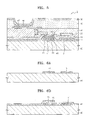
- FIG. 1 is a schematic cross-sectional view of an embodiment of an organic light emitting display apparatus
- FIGS. 2A through 2F are schematic cross-sectional views showing an embodiment of a method of manufacturing the organic light emitting display apparatus of FIG. 1 ;
- FIG. 3 is a schematic cross-sectional view of another embodiment of an organic light emitting display apparatus
- FIGS. 4A and 4B are schematic cross-sectional views showing another embodiment of a method of manufacturing the organic light emitting display apparatus of FIG. 3 ;
- FIG. 5 is a schematic cross-sectional view of an organic light emitting display apparatus according to a comparative example.
- FIGS. 6A through 6G are schematic cross-sectional views showing a method of manufacturing the organic light emitting display apparatus of FIG. 5 , according to the comparative example.
- FIG. 1 is a schematic cross-sectional view of an embodiment of an organic light emitting display apparatus 1.
- FIGS. 2A through 2F are schematic cross-sectional views showing an embodiment of a method of manufacturing the organic light emitting display apparatus 1 of FIG. 1 .
- a pixel region PXL1 having a light emitting layer 119, a thin film transistor (TFT) region TFT1 having a TFT, and a capacitor region CAP 1 having a capacitor are formed on a substrate 10.
- the substrate 10 and a first protection layer 12 are formed.
- the substrate 10 may be formed of a transparent material
- the first protection layer 12 may be formed of an insulating film.
- a gate electrode 213 of the TFT is formed on the first protection layer 12.
- a first insulating layer 14 that functions as a gate insulating film is formed on the gate electrode 213, and a semiconductor layer 215 is formed on the first insulating layer 14.
- the semiconductor layer 215 includes a transparent conductive oxide.
- the transparent oxide may include at least one of gallium (Ga), indium (In), zinc (Zn), hafnium (Hf), and tin (Sn).
- the transparent conductive oxide may be one of InGaZnO, ZnSnO, InZnO, InGaO, ZnO, TiO, and hafnium-indium-zinc oxide (HIZO).
- An oxide semiconductor TFT that includes a transparent conductive oxide, as an active layer has high performance characteristics and can be manufactured using a low temperature process, and thus, is evaluated as an optimum device for a backplane for a flat panel display apparatus.
- the oxide semiconductor TFT has a transparent characteristic in a visible light region and is flexible. Therefore, the oxide semiconductor TFT may be applied to a transparent display apparatus or a flexible display apparatus.
- a second insulating layer 16 covering the semiconductor layer 215 is formed.
- Source and drain electrodes 217 connected to the semiconductor layer 215 through contact holes Cl that penetrate through the second insulating layer 16 are formed on the second insulating layer 16.
- One of the source and drain electrodes 217 is connected to an upper edge of a pixel electrode 111 of the pixel region PXL1 via a via hole C2 that simultaneously penetrates the first protection layer 12, the first insulating layer 14, and the second insulating layer 16.
- the pixel electrode 111 that includes a transparent conductive material is formed on the substrate 10 in the pixel region PXL1.
- the pixel electrode 111 may include at least one of indium tin oxide (ITO), indium zink oxide (IZO), zinc oxide (ZnO), indium oxide (In203), indium gallium oxide (IGO), and aluminum zinc oxide (AZO).
- the pixel electrode 111 may be formed as a multiple layer that includes a semi-transparent metal layer 111a that includes silver (Ag). As depicted in FIG. 1 , the pixel electrode 111 may further include the semi-transparent metal layer 111a that includes silver (Ag) and a layer 111b that includes a transparent conductive material such as ITO on the semi-transparent metal layer 111a.
- the semi-transparent metal layer 111a functions as a semi-transparent mirror and may form a resonance structure together with a facing electrode 120 that functions as a reflection mirror, and thus, can increase optical extraction efficiency of the display apparatus.
- the first protection layer 12 is formed above/on an upper edge of the pixel electrode 111 (i.e. on an edge of the pixel electrode 111 on a side of the pixel electrode 111 that faces away from the substrate).
- the first protection layer 12 may function as a protective film for preventing the pixel electrode 111 from degrading during a manufacturing process of the pixel electrode 111, and may function as a dielectric film of the capacitor.
- the first protection layer 12 may be one of various insulating films formed of a material selected from SiNx, SiOx, and SiON.
- a second protection layer 113 is formed above/on an upper edge of the pixel electrode 111 (i.e. on an edge of the pixel electrode 111 on a side of the pixel electrode 111 that faces away from the substrate) by using the same material used to form the gate electrode 213.
- the first insulating layer 14 and the second insulating layer 16 are sequentially stacked on the second protection layer 113.
- the second protection layer 113, the first insulating layer 14, and the second insulating layer 16 form an opening for exposing the pixel electrode 111.
- Etching surfaces S1 of the opening in the second protection layer 113, the first insulating layer 14, and the second insulating layer 16 form the same plane.
- the second protection layer 113 may function as a protective film for preventing the pixel electrode 111 from degrading during the manufacturing process of the pixel electrode 111.
- a third insulating layer 18 is formed on the second insulating layer 16, and an opening C4 that exposes the pixel electrode 11 1 is formed in the third insulating layer 18.
- Etching surfaces S2 of the third insulating layer 18 and the first protection layer 12 form the same plane. Accordingly, the etching surfaces S2 of the first protection layer 12 and the second protection layer 113 that expose the pixel electrode 111 may form a gap G.
- the light emitting layer 119 is formed on the pixel electrode 111, and light generated from the light emitting layer 119 is emitted towards the substrate 10 through the pixel electrode 111 formed of a transparent conductive material.
- the light emitting layer 119 may be formed of a low molecular organic material or a polymer organic material. If the light emitting layer 119 is formed of a low molecular organic material, a hole transport layer (HTL), a hole injection Layer (HIL), an electron transport layer (ETL), and an electron injection layer (EIL) may be stacked around the light emitting layer 119. Also, various layers may be stacked as necessary.
- the low molecular organic material may include copper phthalocyanine (CuPc), N,N'-di(naphthalene-l-yl)-N,N'-diphenyl-benzidinc (NPB), or tris-8-hydroxyquinoline aluminum (Alq3).
- a hole transport layer HTL may be included in addition to the light emitting layer 119.
- the HTL may be formed of poly-(2,4)-ethylene-dihydroxy thiophene (PEDOT) or polyaniline (PANI).
- the organic material may be a poly organic material such as polyphenylenevinylene (PPV), and polyfluorene.
- the facing electrode 120 as a common electrode is formed on the light emitting layer 119.
- the pixel electrode 111 is used as an anode, and the facing electrode 120 is used as a cathode.
- the polarities of the pixel electrode 111 and the facing electrode 120 may be reversed in other embodiments.
- the facing electrode 120 may be formed as a reflective electrode that includes a reflective material.
- the facing electrode 120 may include at least one of Al, Mg, Li, Ca, LiF/Ca, and LiF/Al. Since the facing electrode 120 is a reflective electrode, light generated from the light emitting layer 119 is reflected by the facing electrode 120 and is emitted towards the substrate 10 through the pixel electrode 111 formed of a transparent conductive material. If the pixel electrode 111 further includes the semi-transparent metal layer 111a that includes silver Ag, the semi-transparent metal layer 111a may function as a semi-transparent mirror, may form a resonance structure together with the facing electrode 120 that functions as a reflection mirror, thereby increasing optical extraction efficiency of the organic light emitting display apparatus 1.
- a capacitor first electrode 311 and a capacitor second electrode 313 are disposed on the substrate 10 with the first protection layer 12 interposed therebetween.
- the capacitor first electrode 311 is formed on the same layer as the pixel electrode 111 1 using the same material used to form the pixel electrode 111.
- the capacitor second electrode 313 is formed on the same layer as the gate electrode 213 using the same material used to form the gate electrode 213.
- the first protection layer 12 functions as a dielectric film. In some embodiments, since the capacitor first electrode 311 and the capacitor second electrode 313 are respectively formed in the same mask process for forming the pixel electrode 111 and the gate electrode 213, the manufacturing process may be simplified.
- the first insulating layer 14 and the second insulating layer 16 are sequentially stacked on the capacitor second electrode 313, and a capacitor third electrode 317 that is formed on the same layer as the source and drain electrodes 217.
- the capacitor 317 may be formed of the same material used to form the source and drain electrodes 217, and may be formed on the second insulating layer 16. Since the capacitor first electrode 311 and the capacitor second electrode 313 form a metal-insulator-metal (MIM) cap, when the area of the capacitor is increased to increase a capacitance, an opening ratio of a display apparatus may be reduced. However, when the capacitor third electrode 317 is additionally formed, the capacitance is increased since the capacitor third electrode 317 is connected in parallel to the capacitor first electrode 311 and the capacitor second electrode 313. Therefore, even though the area of the capacitor is reduced, the reduced capacitance can be compensated for.
- MIM metal-insulator-metal
- FIGS. 2A through 2F are schematic cross-sectional views showing an embodiment of a method of manufacturing the organic light emitting display apparatus 1 of FIG. 1 .
- the pixel electrode 111 and the capacitor first electrode 311 are simultaneously formed on the substrate 10 in a first mask process.
- a buffer layer (not shown) that includes Si0 2 and/or SiNx may further be formed on the substrate 10 to provide planarity to the substrate 10 and to block penetration of foreign elements into the substrate 10.
- FIG. 2A shows a result whereby, after depositing a transparent conductive material on the substrate and coating a photoresist (not shown) on the transparent conductive material, the pixel electrode 111 and the capacitor first electrode 311 are simultaneously patterned by a photolithography process using a first mask (not shown).
- the first mask process using photolithography includes a series of processes such as developing, etching, and stripping or ashing after exposing the first mask (not shown) using an exposure apparatus (not shown).
- the same mask processes using photolithography will not be repeatedly described.
- FIG. 2B is a cross-sectional view of a result of a second mask process of the embodiment of an organic light emitting display apparatus 1.
- the first protection layer 12 is formed on the resultant product of the first mask process, and the second protection layer 113, the gate electrode 213, and the capacitor second electrode 313 are simultaneously formed on the first protection layer 12.
- the second protection layer 113 is not formed in a region where the via hole C2 contacts the pixel electrode 111. Accordingly, the second protection layer 113 has an area smaller than that of the pixel electrode 111.
- FIG. 2C is a cross-sectional view of a resultant product of a third mask process of the embodiment of an organic light emitting display apparatus 1 .
- the first insulating layer 14 is formed on the resultant product of the second mask process, and the semiconductor layer 215 is formed on the first insulating layer 14.
- the semiconductor layer 215 may include a transparent conductive oxide.
- FIG. 2D is a cross-sectional view of a resultant product of a fourth mask process of the embodiment of an organic light emitting display apparatus 1.
- the second insulating layer 16 is formed on the resultant product of the third mask process, and the contact hole C 1 and the via hole C2 are formed.
- an opening C3 that exposes an upper surface of the second protection layer 113 is formed by removing the first insulating layer 14 and the second insulating layer 16. Since the second protection layer 113 is not removed but remains above the pixel electrode 111, the second protection layer 113 protects the first protection layer 12 and the pixel electrode 111 when the contact hole C1, the via hole C2, and the opening C3 are formed.
- FIG. 2E is a cross-sectional view of a resultant product of a fifth mask process of the embodiment of an organic light emitting display apparatus 1 .
- the source and drain electrodes 217 and the capacitor third electrode 317 are formed by patterning the metal material.
- the metal material for forming the source and drain electrodes 217 is also deposited on the opening C3 that is formed in the fourth mask process.
- the metal material is removed together with the second protection layer 113.
- the second protection layer 113 and the metal material are removed by a single etching process. If the second protection layer 113 is formed of a material different from that used to form the source and drain electrodes 217, multiple etching processes may be performed.
- the first protection layer 12 protects the pixel electrode 111.
- FIG. 2F is a cross-sectional view of a resultant product of a sixth mask process of the embodiment of an organic light emitting display apparatus 1.
- the third insulating layer 18 is formed on the resultant product of the fifth mask process, and the opening C4 that exposes an upper surface of the pixel electrode 111 is formed by removing a portion of the third insulating layer 18.
- the first protection layer 12 formed on the pixel electrode 111 is also removed. Accordingly, the third insulating layer 18 and the first protection layer 12 may form the same etching surface S2.
- FIG. 3 is a schematic cross-sectional view of another embodiment of an organic light emitting display apparatus 2.
- FIGS. 4A and 4B are schematic cross-sectional views showing an embodiment of a method of manufacturing the organic light emitting display apparatus 2 of FIG. 3 .
- mainly the differences from the organic light emitting display apparatus 1 will be described.
- FIGS. 4A and 4B are schematic cross-sectional views respectively showing the fifth and sixth mask processes of the organic light emitting display apparatus 2.
- the first through fourth mask processes of the organic light emitting display apparatus 2 are performed the same as described with reference to the organic light emitting display apparatus 1 of FIG. 1 .
- the source and drain electrodes 217 and the capacitor third electrode 317 are formed by patterning the metal material.
- the metal material for forming the source and drain electrodes 217 is also deposited in the opening C3 in the fourth mask process.
- the metal material in the opening C3 is removed together with the second protection layer 113 and the first protection layer 12. Accordingly, since the second protection layer 113 and the first protection layer 12 are etched in the same mask process, the second protection layer 113 and the first protection layer 12 have the same etching surface S3.
- the third insulating layer 18 is formed on the resultant product of the fifth mask process, and the opening C4 that exposes the upper surface of the pixel electrode 111 is formed by removing a portion of the third insulating layer 18.
- the first protection layer 12 since the first protection layer 12 is removed together with the second protection layer 113 in the fifth mask process, the first protection layer 12 and the second protection layer 113 have the same etching surface S3.
- FIG. 5 is a schematic cross-sectional view of an organic light emitting display apparatus 3 according to a comparative example.
- FIGS. 6A through 6G are schematic cross-sectional views showing a method of manufacturing the comparative example of an organic light emitting display apparatus 3 of FIG. 5 .
- FIG. 6A is a schematic cross-sectional view of a result of a first mask process of the organic light emitting display apparatus 3. Referring to FIG. 6A , a gate electrode 41 and a capacitor first electrode 51 of a TFT are simultaneously formed on a substrate 40 in the first mask process.
- FIG. 6B is a schematic cross-sectional view of a result of a second mask process of the organic light emitting display apparatus 3.
- a first insulating layer 42 is formed on the resultant product of the first mask process, and a semiconductor layer 43 that includes a transparent conductive oxide is formed on the first insulating layer 42.
- FIG. 6C is a schematic cross-sectional view of a result of a third mask process of the organic light emitting display apparatus 3.
- a second insulating layer 44 is formed on the resultant product of the second mask process, and contact holes C5 that expose portions of the semiconductor layer 43 are formed.
- FIG. 6D is a schematic cross-sectional view of a result of a fourth mask process of the organic light emitting display apparatus 3.
- the source and drain electrodes 45 are formed by patterning the material.
- a capacitor third electrode 55 is also simultaneously formed.
- FIG. 6E is a schematic cross-sectional view of a result of a fifth mask process of the organic light emitting display apparatus 3.
- a third insulating layer 46 is formed on the resultant product of the fourth mask process, and a via hole C6 that exposes one of the source and drain electrodes 45 is formed.
- FIG. 6F is a schematic cross-sectional view of a result of a sixth mask process of the organic light emitting display apparatus 3.
- the pixel electrode 47 is formed by patterning the material.
- FIG. 6G is a schematic cross-sectional view of a result of a seventh mask process of the organic light emitting display apparatus 3.
- a fourth insulating layer 48 is formed on the resultant product of the sixth mask process, and an opening C7 that exposes an upper surface of the pixel electrode 47 is formed by removing a portion of the fourth insulating layer 48.
- a light emitting layer 49 and a facing electrode 50 are formed in the opening C7 formed in the seventh mask process.
- Embodiments of the present invention are described with reference to an organic light emitting display apparatus, but the present invention is not limited thereto.
- the present invention may also be applied to a liquid crystal display apparatus in which a light emitting layer includes liquid crystals.
- the present invention may also be applied to various kinds of display apparatuses.
Landscapes
- Physics & Mathematics (AREA)
- Engineering & Computer Science (AREA)
- Nonlinear Science (AREA)
- Microelectronics & Electronic Packaging (AREA)
- Crystallography & Structural Chemistry (AREA)
- Chemical & Material Sciences (AREA)
- Mathematical Physics (AREA)
- General Physics & Mathematics (AREA)
- Optics & Photonics (AREA)
- Power Engineering (AREA)
- Geometry (AREA)
- Manufacturing & Machinery (AREA)
- Electroluminescent Light Sources (AREA)
- Devices For Indicating Variable Information By Combining Individual Elements (AREA)
Abstract
Description
- The present disclosure relates to a backplane for a flat panel display apparatus, a flat panel display apparatus including the same, and a method of manufacturing the backplane for the flat panel display apparatus.
- Flat panel display apparatuses, including organic light emitting display apparatuses and liquid crystal display apparatuses, are formed on active type backplanes that include thin film transistors (TFTs) and capacitors formed in each pixel to realize high resolution displays.
- Oxide semiconductor TFTs are evaluated as optimum devices that can be applied to backplanes for flat panel display apparatuses since they have high performance characteristics and can be processed at a low temperature. However, a process for manufacturing backplanes for flat panel display apparatuses that include oxide semiconductors TFT generally includes a plurality of mask processes, thereby increasing manufacturing costs.
- To address the above and/or other problems, the present disclosure provides a backplane that may be manufactured in a simple process and has a high quality display for a flat panel display apparatus, a flat panel display apparatus including the backplane, and a method of manufacturing the backplane.
- According to one aspect, there is provided a backplane for a flat panel display apparatus, the backplane including: a substrate, a pixel electrode that comprises a transparent conductive material on the substrate, a capacitor first electrode formed on the same layer as the pixel electrode, a first protection layer covering the capacitor first electrode and an upper edge of the pixel electrode and, a gate electrode of a thin film transistor (TFT) formed on the first protection layer and a capacitor second electrode formed on the same layer as the gate electrode, a first insulating layer that covers the gate electrode and the capacitor second electrode, a semiconductor layer that is formed on the first insulating layer and comprises a transparent conductive material, a second insulating layer covering the semiconductor layer, source and drain electrodes of the TFT formed on the second insulating layer, where the source and drain electrodes are connected to the semiconductor layer through the second insulating layer, and at least one of the source and drain electrodes is connected to the pixel electrode; and a third insulating layer that covers the source and drain electrodes and exposes the pixel electrode.
- The capacitor first electrode may be formed of the same material used to form the pixel electrode.
- The transparent conductive material may be at least one selected from the group consisting of indium tin oxide (ITO), indium zinc oxide (IZO), zinc oxide (ZnO), indium oxide (In2O3), indium gallium oxide (IGO), and aluminum zinc oxide (AZO).
- The pixel electrode may further include a semi-transparent metal layer.
- The semi-transparent metal layer may include silver Ag.
- The first protection layer may be an insulating layer.
- The capacitor second electrode may be formed of the same material used to form the gate electrode.
- The semiconductor layer may include at least one metal selected from the group consisting of gallium Ga, indium In, zinc Zn, hafnium Hf, and tin Sn and oxygen O2.
- One of the source and drain electrodes may be connected to the pixel electrode through a via hole that simultaneously penetrates through the first protection layer, the first insulating layer, and the second insulating layer.
- The first protection layer, the first insulating layer, and the second insulating layer may form an opening that exposes an upper surface of the pixel electrode. An etch surface of the opening in the first protection layer and etch surfaces of the opening in the first insulating layer and the second insulating layer may be laterally offset from each other so that an upper surface of the first protection layer is exposed.
- The backplane may further include a second protection layer formed of the same material used to form the gate electrode between the first protection layer and the first insulating layer. Etch surfaces of the opening in each of the second protection layer, the first insulating layer, and the second insulating layer may be in the same plane.
- The first protection layer, the first insulating layer, and the second insulating layer may form an opening that exposes an upper surface of the pixel electrode, and etch surfaces of the opening in each of the first protection layer, the first protection layer, the first insulating layer, and the second insulating layer are in the same plane.
- The backplane may further include a second protection layer formed of the same material used to form the gate electrode between the first protection layer and the first insulating layer, wherein etch surfaces of the opening in each of the first protection layer, the second protection layer, the first insulating layer, and the second insulating layer are in the same plane.
- The backplane may further include a capacitor third electrode on the second insulating layer.
- According to another aspect, there is provided a flat panel display apparatus including: the backplane described above, a facing electrode that faces the pixel electrode, and a light emitting unit formed between the pixel electrode and the facing electrode.
- The facing electrode may be a reflection electrode for reflecting light emitted from the light emitting unit.
- The light emitting unit may include an organic light emitting layer.
- According to another aspect, there is provided a method of manufacturing a backplane for a flat panel display apparatus, the method including: forming a pixel electrode and a capacitor first electrode on a substrate through a first mask process; forming a first protection layer covering the pixel electrode and the capacitor first electrode, and forming a gate electrode of a TFT and a capacitor second electrode on the first protection layer through a second mask process; forming a first insulating layer covering the gate electrode and the capacitor second electrode, and forming a semiconductor layer that includes a transparent conductive material on a position corresponding to the gate electrode through a third mask process; forming a second insulating layer covering the semiconductor layer, forming a contact hole that penetrates the second insulating layer and exposes a portion of the semiconductor layer, and forming a via hole that penetrates the first protection layer, the first insulating layer, and the second insulating layer and exposes a portion of the pixel electrode through a fourth mask process; forming source and drain electrodes covering the contact hole and the via hole through a fifth mask process; and forming a third insulating layer covering the source and drain electrodes, and forming an opening that exposes an upper surface of the pixel electrode in the third insulating layer through a sixth mask process.
- The pixel electrode and the capacitor first electrode may be formed of the same material on the same layer.
- The gate electrode of the TFT and the capacitor second electrode may be formed of the same material on the same layer.
- The second mask process may further include forming a second protection layer having an area smaller than that of the pixel electrode on the first protection layer.
- The second protection layer may be formed of the same material used to form the gate electrode and the capacitor second electrode.
- The fourth mask process may include forming an opening that exposes the second protection layer by removing the first insulating layer and the second insulating layer, and where the fifth mask process may include removing the second protection layer, and the sixth mask process may include removing the first protection layer.
- The fourth mask process may include forming an opening that exposes the second protection layer by removing the first insulating layer and the second insulating layer, and where the fifth mask process may include simultaneously removing the first insulating layer and the second insulating layer.
- The fifth mask process may include forming a capacitor third electrode on the same layer as the source and drain electrodes.
- In a backplane according to embodiments of the present invention, a flat panel display apparatus having the backplane, and a method of manufacturing the backplane, the number of masks used is reduced, and accordingly, manufacturing process can be simplified.
- Since a first protection layer is formed on a pixel electrode, damage to the pixel electrode during a manufacturing process can be prevented.
- A capacitance can be increased without increasing an area of capacitors by forming the capacitors in parallel.
- The above and other features and advantages will become more apparent by describing in certain embodiments with reference to the attached drawings in which:
-
FIG. 1 is a schematic cross-sectional view of an embodiment of an organic light emitting display apparatus; -
FIGS. 2A through 2F are schematic cross-sectional views showing an embodiment of a method of manufacturing the organic light emitting display apparatus ofFIG. 1 ; -
FIG. 3 is a schematic cross-sectional view of another embodiment of an organic light emitting display apparatus; -
FIGS. 4A and 4B are schematic cross-sectional views showing another embodiment of a method of manufacturing the organic light emitting display apparatus ofFIG. 3 ; -
FIG. 5 is a schematic cross-sectional view of an organic light emitting display apparatus according to a comparative example; and -
FIGS. 6A through 6G are schematic cross-sectional views showing a method of manufacturing the organic light emitting display apparatus ofFIG. 5 , according to the comparative example. - Certain embodiments of the present invention will now be described more fully with reference to the accompanying drawings. In the drawings, the thicknesses of layers and regions may be exaggerated for clarity, and like reference numerals generally refer to like elements.
-
FIG. 1 is a schematic cross-sectional view of an embodiment of an organic lightemitting display apparatus 1.FIGS. 2A through 2F are schematic cross-sectional views showing an embodiment of a method of manufacturing the organic lightemitting display apparatus 1 ofFIG. 1 . - Referring to
FIG. 1 , in the organic lightemitting display apparatus 1, a pixel region PXL1 having alight emitting layer 119, a thin film transistor (TFT) region TFT1 having a TFT, and acapacitor region CAP 1 having a capacitor are formed on asubstrate 10. - In the TFT region TFT1, the
substrate 10 and afirst protection layer 12 are formed. In some embodiments, thesubstrate 10 may be formed of a transparent material, and thefirst protection layer 12 may be formed of an insulating film. - A
gate electrode 213 of the TFT is formed on thefirst protection layer 12. A firstinsulating layer 14 that functions as a gate insulating film is formed on thegate electrode 213, and asemiconductor layer 215 is formed on the firstinsulating layer 14. - In some embodiments, the
semiconductor layer 215 includes a transparent conductive oxide. The transparent oxide may include at least one of gallium (Ga), indium (In), zinc (Zn), hafnium (Hf), and tin (Sn). In various embodiments, the transparent conductive oxide may be one of InGaZnO, ZnSnO, InZnO, InGaO, ZnO, TiO, and hafnium-indium-zinc oxide (HIZO). An oxide semiconductor TFT that includes a transparent conductive oxide, as an active layer, has high performance characteristics and can be manufactured using a low temperature process, and thus, is evaluated as an optimum device for a backplane for a flat panel display apparatus. The oxide semiconductor TFT has a transparent characteristic in a visible light region and is flexible. Therefore, the oxide semiconductor TFT may be applied to a transparent display apparatus or a flexible display apparatus. - A second insulating
layer 16 covering thesemiconductor layer 215 is formed. Source anddrain electrodes 217 connected to thesemiconductor layer 215 through contact holes Cl that penetrate through the second insulatinglayer 16 are formed on the second insulatinglayer 16. One of the source and drainelectrodes 217 is connected to an upper edge of apixel electrode 111 of the pixel region PXL1 via a via hole C2 that simultaneously penetrates thefirst protection layer 12, the first insulatinglayer 14, and the second insulatinglayer 16. - The
pixel electrode 111 that includes a transparent conductive material is formed on thesubstrate 10 in the pixel region PXL1. Thepixel electrode 111 may include at least one of indium tin oxide (ITO), indium zink oxide (IZO), zinc oxide (ZnO), indium oxide (In203), indium gallium oxide (IGO), and aluminum zinc oxide (AZO). - The
pixel electrode 111 may be formed as a multiple layer that includes asemi-transparent metal layer 111a that includes silver (Ag). As depicted inFIG. 1 , thepixel electrode 111 may further include thesemi-transparent metal layer 111a that includes silver (Ag) and alayer 111b that includes a transparent conductive material such as ITO on thesemi-transparent metal layer 111a. Thesemi-transparent metal layer 111a functions as a semi-transparent mirror and may form a resonance structure together with a facingelectrode 120 that functions as a reflection mirror, and thus, can increase optical extraction efficiency of the display apparatus. - The
first protection layer 12 is formed above/on an upper edge of the pixel electrode 111 (i.e. on an edge of thepixel electrode 111 on a side of thepixel electrode 111 that faces away from the substrate). Thefirst protection layer 12 may function as a protective film for preventing thepixel electrode 111 from degrading during a manufacturing process of thepixel electrode 111, and may function as a dielectric film of the capacitor. Thefirst protection layer 12 may be one of various insulating films formed of a material selected from SiNx, SiOx, and SiON. - A
second protection layer 113 is formed above/on an upper edge of the pixel electrode 111 (i.e. on an edge of thepixel electrode 111 on a side of thepixel electrode 111 that faces away from the substrate) by using the same material used to form thegate electrode 213. The first insulatinglayer 14 and the second insulatinglayer 16 are sequentially stacked on thesecond protection layer 113. Thesecond protection layer 113, the first insulatinglayer 14, and the second insulatinglayer 16 form an opening for exposing thepixel electrode 111. Etching surfaces S1 of the opening in thesecond protection layer 113, the first insulatinglayer 14, and the second insulatinglayer 16 form the same plane. Thesecond protection layer 113 may function as a protective film for preventing thepixel electrode 111 from degrading during the manufacturing process of thepixel electrode 111. - A third insulating
layer 18 is formed on the second insulatinglayer 16, and an opening C4 that exposes the pixel electrode 11 1 is formed in the third insulatinglayer 18. Etching surfaces S2 of the third insulatinglayer 18 and thefirst protection layer 12 form the same plane. Accordingly, the etching surfaces S2 of thefirst protection layer 12 and thesecond protection layer 113 that expose thepixel electrode 111 may form a gap G. - The
light emitting layer 119 is formed on thepixel electrode 111, and light generated from thelight emitting layer 119 is emitted towards thesubstrate 10 through thepixel electrode 111 formed of a transparent conductive material. - The
light emitting layer 119 may be formed of a low molecular organic material or a polymer organic material. If thelight emitting layer 119 is formed of a low molecular organic material, a hole transport layer (HTL), a hole injection Layer (HIL), an electron transport layer (ETL), and an electron injection layer (EIL) may be stacked around thelight emitting layer 119. Also, various layers may be stacked as necessary. The low molecular organic material may include copper phthalocyanine (CuPc), N,N'-di(naphthalene-l-yl)-N,N'-diphenyl-benzidinc (NPB), or tris-8-hydroxyquinoline aluminum (Alq3). In embodiments where thelight emitting layer 119 is formed of a polymer organic material, a hole transport layer HTL may be included in addition to thelight emitting layer 119. The HTL may be formed of poly-(2,4)-ethylene-dihydroxy thiophene (PEDOT) or polyaniline (PANI). The organic material may be a poly organic material such as polyphenylenevinylene (PPV), and polyfluorene. - The facing
electrode 120 as a common electrode is formed on thelight emitting layer 119. In some embodiments, thepixel electrode 111 is used as an anode, and the facingelectrode 120 is used as a cathode. The polarities of thepixel electrode 111 and the facingelectrode 120 may be reversed in other embodiments. - The facing
electrode 120 may be formed as a reflective electrode that includes a reflective material. The facingelectrode 120 may include at least one of Al, Mg, Li, Ca, LiF/Ca, and LiF/Al. Since the facingelectrode 120 is a reflective electrode, light generated from thelight emitting layer 119 is reflected by the facingelectrode 120 and is emitted towards thesubstrate 10 through thepixel electrode 111 formed of a transparent conductive material. If thepixel electrode 111 further includes thesemi-transparent metal layer 111a that includes silver Ag, thesemi-transparent metal layer 111a may function as a semi-transparent mirror, may form a resonance structure together with the facingelectrode 120 that functions as a reflection mirror, thereby increasing optical extraction efficiency of the organic light emittingdisplay apparatus 1. - In the capacitor region CAP1, a capacitor
first electrode 311 and a capacitorsecond electrode 313 are disposed on thesubstrate 10 with thefirst protection layer 12 interposed therebetween. - The capacitor
first electrode 311 is formed on the same layer as thepixel electrode 111 1 using the same material used to form thepixel electrode 111. The capacitorsecond electrode 313 is formed on the same layer as thegate electrode 213 using the same material used to form thegate electrode 213. Thefirst protection layer 12 functions as a dielectric film. In some embodiments, since the capacitorfirst electrode 311 and the capacitorsecond electrode 313 are respectively formed in the same mask process for forming thepixel electrode 111 and thegate electrode 213, the manufacturing process may be simplified. - The first insulating
layer 14 and the second insulatinglayer 16 are sequentially stacked on the capacitorsecond electrode 313, and a capacitorthird electrode 317 that is formed on the same layer as the source and drainelectrodes 217. Thecapacitor 317 may be formed of the same material used to form the source and drainelectrodes 217, and may be formed on the second insulatinglayer 16. Since the capacitorfirst electrode 311 and the capacitorsecond electrode 313 form a metal-insulator-metal (MIM) cap, when the area of the capacitor is increased to increase a capacitance, an opening ratio of a display apparatus may be reduced. However, when the capacitorthird electrode 317 is additionally formed, the capacitance is increased since the capacitorthird electrode 317 is connected in parallel to the capacitorfirst electrode 311 and the capacitorsecond electrode 313. Therefore, even though the area of the capacitor is reduced, the reduced capacitance can be compensated for. - The third insulating
layer 18, which covers the source and drainelectrodes 217 and the capacitorthird electrode 317, is formed and the opening C4 that exposes thepixel electrode 111 is formed in the third insulatinglayer 18. - Hereinafter, an embodiment of a method of manufacturing the organic light emitting
display apparatus 1 will be described with reference toFIGS. 2A through 2F . -
FIGS. 2A through 2F are schematic cross-sectional views showing an embodiment of a method of manufacturing the organic light emittingdisplay apparatus 1 ofFIG. 1 . - Referring to
FIG. 2A , thepixel electrode 111 and the capacitorfirst electrode 311 are simultaneously formed on thesubstrate 10 in a first mask process. A buffer layer (not shown) that includes Si02 and/or SiNx may further be formed on thesubstrate 10 to provide planarity to thesubstrate 10 and to block penetration of foreign elements into thesubstrate 10. - Although the manufacturing process is not shown in detail in
FIG. 2A, FIG. 2A shows a result whereby, after depositing a transparent conductive material on the substrate and coating a photoresist (not shown) on the transparent conductive material, thepixel electrode 111 and the capacitorfirst electrode 311 are simultaneously patterned by a photolithography process using a first mask (not shown). The first mask process using photolithography includes a series of processes such as developing, etching, and stripping or ashing after exposing the first mask (not shown) using an exposure apparatus (not shown). Hereinafter, the same mask processes using photolithography will not be repeatedly described. -
FIG. 2B is a cross-sectional view of a result of a second mask process of the embodiment of an organic light emittingdisplay apparatus 1. - The
first protection layer 12 is formed on the resultant product of the first mask process, and thesecond protection layer 113, thegate electrode 213, and the capacitorsecond electrode 313 are simultaneously formed on thefirst protection layer 12. Thesecond protection layer 113 is not formed in a region where the via hole C2 contacts thepixel electrode 111. Accordingly, thesecond protection layer 113 has an area smaller than that of thepixel electrode 111. -
FIG. 2C is a cross-sectional view of a resultant product of a third mask process of the embodiment of an organic light emittingdisplay apparatus 1 . - The first insulating
layer 14 is formed on the resultant product of the second mask process, and thesemiconductor layer 215 is formed on the first insulatinglayer 14. Thesemiconductor layer 215 may include a transparent conductive oxide. -
FIG. 2D is a cross-sectional view of a resultant product of a fourth mask process of the embodiment of an organic light emittingdisplay apparatus 1. - The second insulating
layer 16 is formed on the resultant product of the third mask process, and thecontact hole C 1 and the via hole C2 are formed. In a region corresponding to the upper side of thepixel electrode 111, an opening C3 that exposes an upper surface of thesecond protection layer 113 is formed by removing the first insulatinglayer 14 and the second insulatinglayer 16. Since thesecond protection layer 113 is not removed but remains above thepixel electrode 111, thesecond protection layer 113 protects thefirst protection layer 12 and thepixel electrode 111 when the contact hole C1, the via hole C2, and the opening C3 are formed. -
FIG. 2E is a cross-sectional view of a resultant product of a fifth mask process of the embodiment of an organic light emittingdisplay apparatus 1 . - After depositing a metal material for forming the source and drain
electrodes 217 covering the contact hole C1, the via hole C2, and the opening C3, the source and drainelectrodes 217 and the capacitorthird electrode 317 are formed by patterning the metal material. - The metal material for forming the source and drain
electrodes 217 is also deposited on the opening C3 that is formed in the fourth mask process. The metal material is removed together with thesecond protection layer 113. At this point, if the material for forming thesecond protection layer 113 is the same material used to form the source and drainelectrodes 217, thesecond protection layer 113 and the metal material are removed by a single etching process. If thesecond protection layer 113 is formed of a material different from that used to form the source and drainelectrodes 217, multiple etching processes may be performed. - In some embodiments, while the material used to form the source and drain
electrodes 217 is removed from the opening C3 formed on thepixel electrode 111, thefirst protection layer 12 protects thepixel electrode 111. -
FIG. 2F is a cross-sectional view of a resultant product of a sixth mask process of the embodiment of an organic light emittingdisplay apparatus 1. - The third insulating
layer 18 is formed on the resultant product of the fifth mask process, and the opening C4 that exposes an upper surface of thepixel electrode 111 is formed by removing a portion of the third insulatinglayer 18. Thefirst protection layer 12 formed on thepixel electrode 111 is also removed. Accordingly, the third insulatinglayer 18 and thefirst protection layer 12 may form the same etching surface S2. - Another embodiment of an organic light emitting
display apparatus 2 will now be described with reference toFIG. 3 . -
FIG. 3 is a schematic cross-sectional view of another embodiment of an organic light emittingdisplay apparatus 2.FIGS. 4A and 4B are schematic cross-sectional views showing an embodiment of a method of manufacturing the organic light emittingdisplay apparatus 2 ofFIG. 3 . Hereinafter, mainly the differences from the organic light emittingdisplay apparatus 1 will be described. -
FIGS. 4A and 4B are schematic cross-sectional views respectively showing the fifth and sixth mask processes of the organic light emittingdisplay apparatus 2. The first through fourth mask processes of the organic light emittingdisplay apparatus 2 are performed the same as described with reference to the organic light emittingdisplay apparatus 1 ofFIG. 1 . - Referring to
FIG. 4A , after depositing a metal material for forming the source and drainelectrodes 217 covering the contact hole C1, the via hole C2, and the opening C3, which are formed in the fourth mask process, the source and drainelectrodes 217 and the capacitorthird electrode 317 are formed by patterning the metal material. - The metal material for forming the source and drain
electrodes 217 is also deposited in the opening C3 in the fourth mask process. The metal material in the opening C3 is removed together with thesecond protection layer 113 and thefirst protection layer 12. Accordingly, since thesecond protection layer 113 and thefirst protection layer 12 are etched in the same mask process, thesecond protection layer 113 and thefirst protection layer 12 have the same etching surface S3. - Referring to
FIG. 4B , the third insulatinglayer 18 is formed on the resultant product of the fifth mask process, and the opening C4 that exposes the upper surface of thepixel electrode 111 is formed by removing a portion of the third insulatinglayer 18. - Accordingly, in the organic light emitting
display apparatus 2, since thefirst protection layer 12 is removed together with thesecond protection layer 113 in the fifth mask process, thefirst protection layer 12 and thesecond protection layer 113 have the same etching surface S3. - Hereinafter, a comparative example will be described with reference to
FIGS. 5 and 6A through 6G .FIG. 5 is a schematic cross-sectional view of an organic light emittingdisplay apparatus 3 according to a comparative example.FIGS. 6A through 6G are schematic cross-sectional views showing a method of manufacturing the comparative example of an organic light emittingdisplay apparatus 3 ofFIG. 5 . -
FIG. 6A is a schematic cross-sectional view of a result of a first mask process of the organic light emittingdisplay apparatus 3. Referring toFIG. 6A , agate electrode 41 and a capacitorfirst electrode 51 of a TFT are simultaneously formed on asubstrate 40 in the first mask process. -
FIG. 6B is a schematic cross-sectional view of a result of a second mask process of the organic light emittingdisplay apparatus 3. Referring toFIG. 6B , a first insulatinglayer 42 is formed on the resultant product of the first mask process, and asemiconductor layer 43 that includes a transparent conductive oxide is formed on the first insulatinglayer 42. -
FIG. 6C is a schematic cross-sectional view of a result of a third mask process of the organic light emittingdisplay apparatus 3. Referring toFIG. 6C , a second insulatinglayer 44 is formed on the resultant product of the second mask process, and contact holes C5 that expose portions of thesemiconductor layer 43 are formed. -
FIG. 6D is a schematic cross-sectional view of a result of a fourth mask process of the organic light emittingdisplay apparatus 3. Referring toFIG. 6D , after depositing a material for forming source and drainelectrodes 45 covering the contact holes C5, the source and drainelectrodes 45 are formed by patterning the material. A capacitorthird electrode 55 is also simultaneously formed. -
FIG. 6E is a schematic cross-sectional view of a result of a fifth mask process of the organic light emittingdisplay apparatus 3. Referring toFIG. 6E , a third insulatinglayer 46 is formed on the resultant product of the fourth mask process, and a via hole C6 that exposes one of the source and drainelectrodes 45 is formed. -
FIG. 6F is a schematic cross-sectional view of a result of a sixth mask process of the organic light emittingdisplay apparatus 3. Referring toFIG. 6F , after depositing a material for forming apixel electrode 47 covering the via hole C6 formed in the fifth mask process, thepixel electrode 47 is formed by patterning the material. -
FIG. 6G is a schematic cross-sectional view of a result of a seventh mask process of the organic light emittingdisplay apparatus 3. Referring toFIG. 6G , a fourth insulatinglayer 48 is formed on the resultant product of the sixth mask process, and an opening C7 that exposes an upper surface of thepixel electrode 47 is formed by removing a portion of the fourth insulatinglayer 48. - Referring to
FIG. 5 , alight emitting layer 49 and a facingelectrode 50 are formed in the opening C7 formed in the seventh mask process. - In the comparative example of the organic light emitting
display apparatus 3, in order to manufacture a backplane that includes a bottom gate type oxide semiconductor, mask processes are performed a total of seven times. However, in the embodiments of organic light emittingdisplay apparatuses pixel electrode 111, or a total of six times, including the sixth mask process for forming the opening C4 that exposes thepixel electrode 111 by patterning the third insulatinglayer 18. Accordingly, as a result of the reduction of mask processes, manufacturing costs may be greatly reduced. - Embodiments of the present invention are described with reference to an organic light emitting display apparatus, but the present invention is not limited thereto. The present invention may also be applied to a liquid crystal display apparatus in which a light emitting layer includes liquid crystals. The present invention may also be applied to various kinds of display apparatuses.
- While the present invention has been particularly shown and described with reference to certain embodiments thereof, it will be understood by those of ordinary skill in the art that various changes in form and details may be made therein without departing from the scope of the present invention as defined by the following claims.
Claims (25)
- A backplane for a flat panel display apparatus, the backplane comprising:a substrate;a pixel electrode that comprises a transparent conductive material on the substrate;a capacitor first electrode formed on the same layer as the pixel electrode;a first protection layer covering the capacitor first electrode and an upper edge of the pixel electrode;a gate electrode of a thin film transistor, hereinafter referred to as TFT, formed on the first protection layer,a capacitor second electrode formed on the same layer as the gate electrode;a first insulating layer that covers the gate electrode and the capacitor second electrode;a semiconductor layer that is formed on the first insulating layer and comprises a transparent conductive material;a second insulating layer covering the semiconductor layer;source and drain electrodes of the TFT formed on the second insulating layer, wherein the source and drain electrodes are connected to the semiconductor layer through the second insulating layer, and at least one of the source and drain electrodes is connected to the pixel electrode; anda third insulating layer that covers the source and drain electrodes and exposes the pixel electrode.
- The backplane of claim 1, wherein the capacitor first electrode is formed of the same material used to form the pixel electrode.
- The backplane of claim 1 or 2, wherein the transparent conductive material is at least one selected from the group consisting of indium tin oxide, indium zink oxide, zink oxide, indium oxide, indium galium oxide, and aluminium zink oxide.
- The backplane of claim 1, 2 or 3, wherein the pixel electrode further comprises a semi-transparent metal layer.
- The backplane of claim 4, wherein the semi-transparent metal layer comprises silver.
- The backplane of any preceding claim, wherein the first protection layer is an insulating layer.
- The backplane of any preceding claim, wherein the capacitor second electrode is formed of the same material used to form the gate electrode.
- The backplane of any preceding claim, wherein the semiconductor layer comprises at least one material selected from the group consisting of gallium, indium, zinc, hafnium, and tin and oxygen.
- The backplane of any preceding claim, wherein one of the source and drain electrodes is connected to the pixel electrode through a via hole that simultaneously penetrates through the first protection layer, the first insulating layer, and the second insulating layer.
- The backplane of any preceding claim, wherein the first protection layer, the first insulating layer, and the second insulating layer form an opening that exposes an upper surface of the pixel electrode, wherein an etch surface of the opening in the first protection layer, and etch surfaces of the oping in the first insulating layer and the second insulating layer are laterally offset from each other.
- The backplane of claim 10, further comprising a second protection layer formed of the same material used to form the gate electrode between the first protection layer and the first insulating layer, wherein etch surfaces of the opening in each of the second protection layer, the first insulating layer, and the second insulating layer are in the same plane.
- The backplane of any of claims 1 to 9, wherein the first protection layer, the first insulating layer, and the second insulating layer form an opening that exposes an upper surface of the pixel electrode, and etch surfaces of the opening in each of the first protection layer, the first insulating layer, and the second insulating layer are in the same plane.
- The backplane of claim 12, further comprising a second protection layer formed of the same material used to form the gate electrode between the first protection layer and the first insulating layer, wherein etch surfaces of the opening in each of the first protection layer, the second protection layer, the first insulating layer, and the second insulating layer are in the same plane.
- The backplane of claim 12 or 13, further comprising a capacitor third electrode on the second insulating layer.
- A flat panel display apparatus comprising:the backplane of claim 1;a facing electrode that faces the pixel electrode; anda light emitting unit formed between the pixel electrode and the facing electrode.
- The flat panel display apparatus of claim 15, wherein the facing electrode is a reflection electrode for reflecting light emitted from the light emitting unit.
- The flat panel display apparatus of claim 15 or 16, wherein the light emitting unit comprises an organic light emitting layer.
- A method of manufacturing a backplane for a flat panel display apparatus, the method comprising:forming a pixel electrode and a capacitor first electrode on a substrate through a first mask process;forming a first protection layer covering the pixel electrode and the capacitor first electrode, and forming a gate electrode of a TFT and a capacitor second electrode on the first protection layer through a second mask process;forming a first insulating layer covering the gate electrode and the capacitor second electrode, and forming a semiconductor layer that comprises a transparent conductive material on a position corresponding to the gate electrode through a third mask process;forming a second insulating layer covering the semiconductor layer, forming a contact hole that penetrates the second insulating layer and exposes a portion of the semiconductor layer, and forming a via hole that penetrates the first protection layer, the first insulating layer, and the second insulating layer and exposes a portion of the pixel electrode through a fourth mask process;forming source and drain electrodes covering the contact hole and the via hole through a fifth mask process; andforming a third insulating layer covering the source and drain electrodes, and forming an opening that exposes an upper surface of the pixel electrode in the third insulating layer through a sixth mask process.
- The method of claim 18, wherein the pixel electrode and the capacitor first electrode are formed of the same material on the same layer.
- The method of claim 18 or 19, wherein the gate electrode of the TFT and the capacitor second electrode are formed of the same material on the same layer.
- The method of claim 18, 19 or 20, wherein the second mask process comprises forming a second protection layer having an area smaller than that of the pixel electrode on the first protection layer.
- The method of claim 21, wherein the second protection layer is formed of the same material used to form the gate electrode and the capacitor second electrode.
- The method of claim 21 or 22, wherein the fourth mask process comprises forming an opening that exposes the second protection layer by removing the first insulating layer and the second insulating layer, and wherein the fifth mask process comprises removing the second protection layer, and the sixth mask process comprises removing the first protection layer.
- The method of claim 21 or 22, wherein the fourth mask process comprises forming an opening that exposes the second protection layer by removing the first insulating layer and the second insulating layer, and wherein the fifth mask process comprises simultaneously removing the first insulating layer and the second insulating layer.
- The method of any of claims 18 to 24, wherein the fifth mask process comprises forming a capacitor third electrode on the same layer as the source and drain electrodes.
Applications Claiming Priority (1)
| Application Number | Priority Date | Filing Date | Title |
|---|---|---|---|
| KR1020110047944A KR20120129592A (en) | 2011-05-20 | 2011-05-20 | Backplane for flat panel display apparatus, flat panel display apparatus comprising the same, and manufacturing method of the backplane for flat panel display apparatus |
Publications (2)
| Publication Number | Publication Date |
|---|---|
| EP2525405A2 true EP2525405A2 (en) | 2012-11-21 |
| EP2525405A3 EP2525405A3 (en) | 2014-08-27 |
Family
ID=46062157
Family Applications (1)
| Application Number | Title | Priority Date | Filing Date |
|---|---|---|---|
| EP12168449.2A Withdrawn EP2525405A3 (en) | 2011-05-20 | 2012-05-17 | Backplane for flat panel display apparatus, flat panel display apparatus, and method of manufacturing the backplane |
Country Status (6)
| Country | Link |
|---|---|
| US (2) | US8618546B2 (en) |
| EP (1) | EP2525405A3 (en) |
| JP (1) | JP6054629B2 (en) |
| KR (1) | KR20120129592A (en) |
| CN (1) | CN102842582B (en) |
| TW (1) | TWI529948B (en) |
Cited By (2)
| Publication number | Priority date | Publication date | Assignee | Title |
|---|---|---|---|---|
| WO2016170355A1 (en) * | 2015-04-22 | 2016-10-27 | Flexenable Limited | A control component for a current-driven optical media |
| US11605655B2 (en) | 2014-02-27 | 2023-03-14 | Semiconductor Energy Laboratory Co., Ltd. | Semiconductor device, and module and electronic appliance including the same |
Families Citing this family (23)
| Publication number | Priority date | Publication date | Assignee | Title |
|---|---|---|---|---|
| KR20120129592A (en) * | 2011-05-20 | 2012-11-28 | 삼성디스플레이 주식회사 | Backplane for flat panel display apparatus, flat panel display apparatus comprising the same, and manufacturing method of the backplane for flat panel display apparatus |
| KR102021028B1 (en) * | 2012-12-04 | 2019-09-16 | 삼성디스플레이 주식회사 | Organic light emitting display device |
| KR102015873B1 (en) * | 2013-01-03 | 2019-10-22 | 삼성디스플레이 주식회사 | Back plane of display and manufacturing method for the same |
| JP5948427B2 (en) * | 2013-03-18 | 2016-07-06 | パナソニック株式会社 | Thin film semiconductor substrate, light emitting panel, and method of manufacturing thin film semiconductor substrate |
| TWI502784B (en) * | 2013-03-21 | 2015-10-01 | Chunghwa Picture Tubes Ltd | Manufacturing method of electrode substrate for electroluminescent device and manufacturing method of electroluminescent device |
| KR102049443B1 (en) * | 2013-05-15 | 2019-11-28 | 삼성디스플레이 주식회사 | Organic light emitting display device and method of manufacturing thereof |
| KR102116493B1 (en) * | 2013-05-23 | 2020-06-08 | 삼성디스플레이 주식회사 | Organinc light emitting display device and manufacturing method for the same |
| KR102093458B1 (en) | 2013-07-05 | 2020-03-26 | 삼성디스플레이 주식회사 | Capacitor |
| JP6169005B2 (en) * | 2014-01-17 | 2017-07-26 | 株式会社ジャパンディスプレイ | Light emitting element display device |
| US20150349000A1 (en) * | 2014-05-29 | 2015-12-03 | Qualcomm Mems Technologies, Inc. | Fabrication of transistor with high density storage capacitor |
| KR102236381B1 (en) | 2014-07-18 | 2021-04-06 | 삼성디스플레이 주식회사 | Organic light emitting display device and method of manufacturing an organic light emitting display device |
| CN104157613B (en) * | 2014-07-31 | 2017-03-08 | 京东方科技集团股份有限公司 | A kind of preparation method of array base palte |
| TWI582968B (en) | 2014-08-15 | 2017-05-11 | 群創光電股份有限公司 | Array substrate structure and contact structure |
| US9766517B2 (en) * | 2014-09-05 | 2017-09-19 | Semiconductor Energy Laboratory Co., Ltd. | Display device and display module |
| KR102360783B1 (en) | 2014-09-16 | 2022-02-10 | 삼성디스플레이 주식회사 | display device |
| KR102284756B1 (en) | 2014-09-23 | 2021-08-03 | 삼성디스플레이 주식회사 | display device |
| KR102460407B1 (en) * | 2015-10-30 | 2022-10-27 | 엘지디스플레이 주식회사 | Organic light emitting display device and method of manufacturing the same |
| KR102581258B1 (en) * | 2016-06-10 | 2023-09-22 | 삼성디스플레이 주식회사 | Organic light emitting display device and method for manufacturing the same |
| CN107579083B (en) * | 2017-09-30 | 2024-06-11 | 京东方科技集团股份有限公司 | Array substrate, manufacturing method and display device |
| CN107887398B (en) * | 2017-11-14 | 2022-01-21 | 京东方科技集团股份有限公司 | Array substrate, preparation method thereof, display panel and display device |
| KR102503168B1 (en) * | 2018-02-08 | 2023-02-27 | 삼성디스플레이 주식회사 | Display device and fabricating method thereof |
| KR20240117936A (en) * | 2023-01-26 | 2024-08-02 | 엘지디스플레이 주식회사 | Display device |
| KR20240176890A (en) * | 2023-06-16 | 2024-12-26 | 삼성디스플레이 주식회사 | Display device and method of manufacturing the same |
Family Cites Families (35)
| Publication number | Priority date | Publication date | Assignee | Title |
|---|---|---|---|---|
| US4528480A (en) * | 1981-12-28 | 1985-07-09 | Nippon Telegraph & Telephone | AC Drive type electroluminescent display device |
| JP4030193B2 (en) * | 1998-07-16 | 2008-01-09 | 株式会社半導体エネルギー研究所 | Method for manufacturing semiconductor device |
| TWI232595B (en) * | 1999-06-04 | 2005-05-11 | Semiconductor Energy Lab | Electroluminescence display device and electronic device |
| KR100395755B1 (en) * | 2001-06-28 | 2003-08-21 | 삼성전자주식회사 | Non-volatile memory device and method of fabricating the same |
| TWI270919B (en) * | 2002-04-15 | 2007-01-11 | Semiconductor Energy Lab | Display device and method of fabricating the same |
| JP2004192935A (en) * | 2002-12-11 | 2004-07-08 | Hitachi Displays Ltd | Organic EL display |
| KR100521272B1 (en) * | 2002-12-20 | 2005-10-12 | 삼성에스디아이 주식회사 | OELD with improved brightness |
| KR100557730B1 (en) * | 2003-12-26 | 2006-03-06 | 엘지.필립스 엘시디 주식회사 | Dual panel type organic electroluminescent device and manufacturing method thereof |
| US8629819B2 (en) * | 2005-07-14 | 2014-01-14 | Semiconductor Energy Laboratory Co., Ltd. | Semiconductor device and driving method thereof |
| JP5132097B2 (en) * | 2005-07-14 | 2013-01-30 | 株式会社半導体エネルギー研究所 | Display device |
| JP5060738B2 (en) * | 2006-04-28 | 2012-10-31 | 株式会社ジャパンディスプレイイースト | Image display device |
| KR20080058762A (en) | 2006-12-22 | 2008-06-26 | 엘지디스플레이 주식회사 | Array substrate for thin film transistor liquid crystal display device and manufacturing method thereof |
| JP5275608B2 (en) * | 2007-10-19 | 2013-08-28 | 株式会社半導体エネルギー研究所 | Method for manufacturing semiconductor substrate |
| KR100964227B1 (en) * | 2008-05-06 | 2010-06-17 | 삼성모바일디스플레이주식회사 | Thin film transistor array substrate for flat panel display, organic light emitting display device comprising same, and manufacturing method thereof |
| CN102047426B (en) * | 2008-05-29 | 2013-02-06 | 夏普株式会社 | Semiconductor device and manufacturing method thereof |
| KR101545923B1 (en) | 2008-11-26 | 2015-08-21 | 엘지디스플레이 주식회사 | Oxide thin film transistor and manufacturing method thereof |
| KR101251725B1 (en) * | 2008-12-18 | 2013-04-05 | 파나소닉 주식회사 | Organic electroluminescence display device and method for manufacturing same |
| US8441007B2 (en) * | 2008-12-25 | 2013-05-14 | Semiconductor Energy Laboratory Co., Ltd. | Display device and manufacturing method thereof |
| JP2010177223A (en) * | 2009-01-27 | 2010-08-12 | Videocon Global Ltd | Liquid crystal display device and method of manufacturing the same |
| KR101074788B1 (en) * | 2009-01-30 | 2011-10-20 | 삼성모바일디스플레이주식회사 | Flat panel display apparatus and the manufacturing method thereof |
| JP2010204239A (en) * | 2009-03-02 | 2010-09-16 | Seiko Epson Corp | Liquid crystal device and electronic apparatus |
| KR101050461B1 (en) * | 2009-04-23 | 2011-07-19 | 삼성모바일디스플레이주식회사 | Organic light emitting display device and manufacturing method of organic light emitting display device |
| KR101646808B1 (en) * | 2009-10-28 | 2016-08-08 | 가부시키가이샤 제이올레드 | Lens sheet, display panel device, and display device |
| KR101093424B1 (en) * | 2009-11-10 | 2011-12-14 | 삼성모바일디스플레이주식회사 | Organic light emitting display device and manufacturing method thereof |
| KR101117642B1 (en) * | 2009-11-16 | 2012-03-05 | 삼성모바일디스플레이주식회사 | Organic light emitting diode display and method for manufacturing the same |
| KR101108176B1 (en) * | 2010-07-07 | 2012-01-31 | 삼성모바일디스플레이주식회사 | Double gate type thin film transistor and organic light emitting display device having same |
| JP5574456B2 (en) * | 2010-08-06 | 2014-08-20 | パナソニック株式会社 | LIGHT EMITTING ELEMENT, MANUFACTURING METHOD THEREOF, AND LIGHT EMITTING DEVICE |
| KR101764272B1 (en) * | 2010-12-02 | 2017-08-16 | 삼성디스플레이 주식회사 | Organic light emitting display device and manufacturing method thereof |
| KR20120129592A (en) * | 2011-05-20 | 2012-11-28 | 삼성디스플레이 주식회사 | Backplane for flat panel display apparatus, flat panel display apparatus comprising the same, and manufacturing method of the backplane for flat panel display apparatus |
| KR101873448B1 (en) * | 2011-07-15 | 2018-07-03 | 삼성디스플레이 주식회사 | Organinc light emitting display device and manufacturing method for the same |
| KR101801350B1 (en) * | 2011-08-01 | 2017-12-21 | 삼성디스플레이 주식회사 | Thin-film transistor array substrate, organic light emitting display device comprising the same and manufacturing method of the same |
| KR101810051B1 (en) * | 2011-08-09 | 2017-12-19 | 삼성디스플레이 주식회사 | Organic light emitting display and the manufacturing method thereof |
| KR102080009B1 (en) * | 2013-05-29 | 2020-04-08 | 삼성디스플레이 주식회사 | Organic light emitting display apparatus and the manufacturing method thereof |
| CN103928470B (en) * | 2013-06-24 | 2017-06-13 | 上海天马微电子有限公司 | A kind of oxide semiconductor TFT array substrate and its manufacturing method |
| KR20150000949A (en) * | 2013-06-25 | 2015-01-06 | 삼성디스플레이 주식회사 | Display device and manufacturing method of the same |
-
2011
- 2011-05-20 KR KR1020110047944A patent/KR20120129592A/en not_active Abandoned
-
2012
- 2012-04-11 US US13/444,736 patent/US8618546B2/en active Active
- 2012-05-10 TW TW101116699A patent/TWI529948B/en active
- 2012-05-16 JP JP2012112741A patent/JP6054629B2/en active Active
- 2012-05-17 EP EP12168449.2A patent/EP2525405A3/en not_active Withdrawn
- 2012-05-21 CN CN201210158797.9A patent/CN102842582B/en active Active
-
2013
- 2013-11-20 US US14/085,211 patent/US9048257B2/en active Active
Non-Patent Citations (1)
| Title |
|---|
| None |
Cited By (4)
| Publication number | Priority date | Publication date | Assignee | Title |
|---|---|---|---|---|
| US11605655B2 (en) | 2014-02-27 | 2023-03-14 | Semiconductor Energy Laboratory Co., Ltd. | Semiconductor device, and module and electronic appliance including the same |
| US11916088B2 (en) | 2014-02-27 | 2024-02-27 | Semiconductor Energy Laboratory Co., Ltd. | Semiconductor device, and module and electronic appliance including the same |
| WO2016170355A1 (en) * | 2015-04-22 | 2016-10-27 | Flexenable Limited | A control component for a current-driven optical media |
| US10971062B2 (en) | 2015-04-22 | 2021-04-06 | Flexenable Limited | Control component for a current-driven optical media |
Also Published As
| Publication number | Publication date |
|---|---|
| TW201248865A (en) | 2012-12-01 |
| EP2525405A3 (en) | 2014-08-27 |
| US8618546B2 (en) | 2013-12-31 |
| CN102842582B (en) | 2016-09-07 |
| KR20120129592A (en) | 2012-11-28 |
| US20120292612A1 (en) | 2012-11-22 |
| US20140080270A1 (en) | 2014-03-20 |
| JP6054629B2 (en) | 2016-12-27 |
| CN102842582A (en) | 2012-12-26 |
| TWI529948B (en) | 2016-04-11 |
| JP2012242834A (en) | 2012-12-10 |
| US9048257B2 (en) | 2015-06-02 |
Similar Documents
| Publication | Publication Date | Title |
|---|---|---|
| US9048257B2 (en) | Backplane for flat panel display apparatus, flat panel display apparatus, and method of manufacturing the backplane | |
| US9502604B2 (en) | Backplane for flat panel display apparatus, method of manufacturing the backplane, and organic light emitting display apparatus including the backplane | |
| US8575606B2 (en) | Back panel for flat panel display apparatus, flat panel display apparatus comprising the same, and method of manufacturing the back panel | |
| KR101833235B1 (en) | Thin-film transistor array substrate, organic light emitting display device comprising the same and manufacturing method of the same | |
| US8785937B2 (en) | Organic light-emitting display apparatus and method of manufacturing the same | |
| US8637868B2 (en) | Thin-film transistor array substrate, organic light emitting display device including the same, and method of manufacturing the same | |
| KR101881895B1 (en) | Thin-film transistor array substrate, organic light emitting display device comprising the same and method for manufacturing of the thin-film transistor array substrate | |
| US9123594B2 (en) | Organic light-emitting display apparatus having high aperture ratio | |
| KR101890799B1 (en) | Thin-film transistor array substrate, organic light emitting display device comprising the same and manufacturing method of the same | |
| KR101938761B1 (en) | Thin-film transistor array substrate, organic light emitting display device comprising the same and manufacturing method of the same | |
| US20130037783A1 (en) | Organic light-emitting display apparatus and method of manufacturing the same | |
| KR20130007310A (en) | Organic light emitting display device, organic light emitting display appratus and manufacturing method of the same | |
| KR20160081100A (en) | Manufacturing method for organic light-emitting display apparatus and the Organic light-emitting display apparatus manufactured by the same method | |
| KR102124044B1 (en) | Thin-film transistor array substrate, manufacturing method thereof, and organic light emitting display apparatus | |
| KR101944916B1 (en) | Thin-film transistor array substrate, organic light emitting display device comprising the same and manufacturing method of the same | |
| KR20140125181A (en) | Back palne of flat panel display and manufacturing method for the same |
Legal Events
| Date | Code | Title | Description |
|---|---|---|---|
| PUAI | Public reference made under article 153(3) epc to a published international application that has entered the european phase |
Free format text: ORIGINAL CODE: 0009012 |
|
| AK | Designated contracting states |
Kind code of ref document: A2 Designated state(s): AL AT BE BG CH CY CZ DE DK EE ES FI FR GB GR HR HU IE IS IT LI LT LU LV MC MK MT NL NO PL PT RO RS SE SI SK SM TR |
|
| AX | Request for extension of the european patent |
Extension state: BA ME |
|
| 17P | Request for examination filed |
Effective date: 20140331 |
|
| RBV | Designated contracting states (corrected) |
Designated state(s): AL AT BE BG CH CY CZ DE DK EE ES FI FR GB GR HR HU IE IS IT LI LT LU LV MC MK MT NL NO PL PT RO RS SE SI SK SM TR |
|
| PUAL | Search report despatched |
Free format text: ORIGINAL CODE: 0009013 |
|
| AK | Designated contracting states |
Kind code of ref document: A3 Designated state(s): AL AT BE BG CH CY CZ DE DK EE ES FI FR GB GR HR HU IE IS IT LI LT LU LV MC MK MT NL NO PL PT RO RS SE SI SK SM TR |
|
| AX | Request for extension of the european patent |
Extension state: BA ME |
|
| RIC1 | Information provided on ipc code assigned before grant |
Ipc: H01L 27/12 20060101AFI20140722BHEP Ipc: H01L 29/66 20060101ALI20140722BHEP |
|
| RAP1 | Party data changed (applicant data changed or rights of an application transferred) |
Owner name: SAMSUNG DISPLAY CO., LTD. |
|
| STAA | Information on the status of an ep patent application or granted ep patent |
Free format text: STATUS: THE APPLICATION HAS BEEN WITHDRAWN |
|
| 18W | Application withdrawn |
Effective date: 20170823 |