EP2525246A1 - Display device - Google Patents
Display device Download PDFInfo
- Publication number
- EP2525246A1 EP2525246A1 EP12168092A EP12168092A EP2525246A1 EP 2525246 A1 EP2525246 A1 EP 2525246A1 EP 12168092 A EP12168092 A EP 12168092A EP 12168092 A EP12168092 A EP 12168092A EP 2525246 A1 EP2525246 A1 EP 2525246A1
- Authority
- EP
- European Patent Office
- Prior art keywords
- shutter
- substrates
- pair
- wall portion
- display device
- Prior art date
- Legal status (The legal status is an assumption and is not a legal conclusion. Google has not performed a legal analysis and makes no representation as to the accuracy of the status listed.)
- Withdrawn
Links
Images


Classifications
-
- G—PHYSICS
- G02—OPTICS
- G02B—OPTICAL ELEMENTS, SYSTEMS OR APPARATUS
- G02B6/00—Light guides; Structural details of arrangements comprising light guides and other optical elements, e.g. couplings
- G02B6/24—Coupling light guides
- G02B6/26—Optical coupling means
- G02B6/35—Optical coupling means having switching means
- G02B6/351—Optical coupling means having switching means involving stationary waveguides with moving interposed optical elements
- G02B6/353—Optical coupling means having switching means involving stationary waveguides with moving interposed optical elements the optical element being a shutter, baffle, beam dump or opaque element
-
- G—PHYSICS
- G02—OPTICS
- G02B—OPTICAL ELEMENTS, SYSTEMS OR APPARATUS
- G02B26/00—Optical devices or arrangements for the control of light using movable or deformable optical elements
- G02B26/004—Optical devices or arrangements for the control of light using movable or deformable optical elements based on a displacement or a deformation of a fluid
-
- G—PHYSICS
- G02—OPTICS
- G02B—OPTICAL ELEMENTS, SYSTEMS OR APPARATUS
- G02B26/00—Optical devices or arrangements for the control of light using movable or deformable optical elements
- G02B26/02—Optical devices or arrangements for the control of light using movable or deformable optical elements for controlling the intensity of light
- G02B26/023—Optical devices or arrangements for the control of light using movable or deformable optical elements for controlling the intensity of light comprising movable attenuating elements, e.g. neutral density filters
-
- G—PHYSICS
- G02—OPTICS
- G02B—OPTICAL ELEMENTS, SYSTEMS OR APPARATUS
- G02B26/00—Optical devices or arrangements for the control of light using movable or deformable optical elements
- G02B26/02—Optical devices or arrangements for the control of light using movable or deformable optical elements for controlling the intensity of light
- G02B26/04—Optical devices or arrangements for the control of light using movable or deformable optical elements for controlling the intensity of light by periodically varying the intensity of light, e.g. using choppers
-
- G—PHYSICS
- G02—OPTICS
- G02B—OPTICAL ELEMENTS, SYSTEMS OR APPARATUS
- G02B6/00—Light guides; Structural details of arrangements comprising light guides and other optical elements, e.g. couplings
- G02B6/24—Coupling light guides
- G02B6/26—Optical coupling means
- G02B6/35—Optical coupling means having switching means
- G02B6/3564—Mechanical details of the actuation mechanism associated with the moving element or mounting mechanism details
- G02B6/3584—Mechanical details of the actuation mechanism associated with the moving element or mounting mechanism details constructional details of an associated actuator having a MEMS construction, i.e. constructed using semiconductor technology such as etching
Definitions
- the present invention relates to a display device.
- a micro-electro-mechanical system (MEMS) display is a display expected to replace a liquid crystal display (see Japanese Patent Application Laid-open No. 2008-197668 ).
- This display differs from a liquid crystal shutter type display utilizing polarization, and displays an image by opening and closing a light transmissive window using a mechanical shutter system.
- One shutter is opened/closed to enable ON/OFF operation for one pixel.
- the shutter is operated by an electrostatic attractive force.
- the shutter is arranged in a space surrounded by a sealing member between a pair of light transmissive substrates, and the space is filled with oil.
- the oil is used to prevent a spring for driving the shutter from sticking, and to reduce a difference in optical refraction index with respect to the light transmissive substrates.
- the present invention has an object to prevent shutter damage to be caused by oil flow.
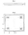
- FIG. 1 is a side view of a display device according to the embodiment of the present invention.
- the display device includes a pair of substrates 10 and 12 having light transmissivity (for example, glass substrates).
- the pair of substrates 10 and 12 are arranged so as to be opposed to each other at an interval (see FIG. 4 ).
- FIG. 2 is a plan view of the display device illustrated in FIG. 1 .
- the upper substrate 10 is represented by a virtual line to show the inner structure.
- a plurality of (large number of) shutters 14 are provided on the lower substrate 12.
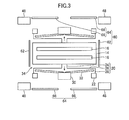
- FIG. 3 is a plan view of the shutter and a drive portion thereof.
- the shutter 14 is a plate which is made of aninorganic material such as semiconductor or a metal, and includes a drive aperture 16. Light is allowed to pass through the drive aperture 16, and is blocked at a part other than the drive aperture 16 of the shutter 14.
- the drive aperture 16 has a shape long in one direction. Note that, as illustrated in FIG. 1 , light is supplied from a backlight unit 18 lying under the substrates.
- the shutter 14 is supported by a first spring 20 to be suspended above the substrate 12 (see FIG. 4 ).
- a plurality of (four in FIG. 3 ) first springs 20 support the shutter 14.
- the first spring 20 is fixed to the substrate 12 by a first fixation portion 22.
- the first spring 20 is made of an elastically deformable material, and is arranged so as to be deformable in a direction parallel to the plate surface of the shutter 14.
- the first spring 20 includes a first portion 24 extending in a direction separating from the shutter 14 (direction intersecting (for example, orthogonal to) the length direction of the drive aperture 16), a second portion 26 extending in a direction along the length direction of the drive aperture 16 outwardly from a center of the drive aperture 16 in the length direction, and a third portion 28 further extending in the direction separating from the shutter 14 (direction intersecting (for example, orthogonal to) the length direction of the drive aperture 16).
- the shutter 14 is supported by the first spring 20 so as to be movable in the direction intersecting (for example, orthogonal to) the length direction of the drive aperture 16.
- the substrate 12 is provided with a second spring 32 supported by a second fixation portion 30.
- the second spring 32 is opposed to the second portion 26 of the first spring 20 on a side separated from the shutter 14 with respect to the second portion 26.
- a voltage is applied to the second fixation portion 30, due to the electrostatic attractive force caused by the potential difference between the second fixation portion 30 and the second portion 26 of the the first spring 20, the second portion 26 is attracted toward the second fixation portion 30.
- the shutter 14 is also attracted via the first portion 24 provided integrally with the second portion 26. That is, the first spring 20 and the second spring 32 are provided for constituting a drive portion 34 for driving the shutter 14 to linearly reciprocate (driving the shutter 14 in a predetermined direction).
- the drive portion 34 is also made of an inorganic material such as semiconductor or a metal.
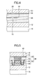
- FIG. 4 is a sectional view of a part of the display device including the shutter.
- the upper substrate 10 has a light shielding film 36 formed thereon.
- a fixed aperture 38 is formed in the light shielding film 36.
- the above-mentioned drive aperture 16 of the shutter 14 and the fixed aperture 38 of the light shielding film 36 are arranged at positions opposed to each other. Light is allowed to pass when both of the apertures communicate with each other, and light is blocked when the fixed aperture 38 of the light shielding film 36 is covered due to the movement of the shutter 14. In other words, the shutter 14 is mechanically driven so as to control the passage and blocking of light through the fixed aperture 38 of the light shielding film 36.
- One drive aperture 16 and one fixed aperture 38 corresponding to each other constitute one pixel, and an image is displayed by a large number of pixels. Therefore, the plurality of (large number of) shutters 14 are provided.
- the shutters 14 and the drive portions 34 thereof are arranged in a display region which displays an image depending on the presence/absence and intensity of light passing through the drive aperture 16 and the fixed aperture 38.
- the pair of substrates 10 and 12 are fixed at an interval with a sealing member 40 illustrated in FIG. 2 .
- the sealing member 40 is provided in close contact with opposed surfaces of the pair of substrates 10 and 12. Further, as illustrated in FIG. 2 , the sealing member 40 includes an opening 42 and is formed so as to surround a space. An end seal 44 closes the opening 42 of the sealing member 40, thereby encapsulating the space surrounded by the sealing member 40 to form an encapsulation space.
- oil 46 for example, silicone oil
- the shutter 14 and the drive portion 34 are arranged in the oil 46.
- the oil 46 can suppress vibrations caused by the movement of the shutter 14 and the drive portion 34, and also can prevent sticking of the first spring 20 and the second spring 32.
- the substrates 10 and 12 are made of glass, with use of the oil 46 having a refractive index close to that of glass, through filling of the oil 46, it is possible to reduce light reflection at an interface of the pair of substrates 10 and 12.
- the display device includes a spacer 48 for maintaining an interval between the pair of substrates 10 and 12.
- FIG. 5 is a sectional view of a part of the display device including the spacer.
- the spacer 48 is arranged in the oil 46 as well.
- the spacer 48 is provided offset from the shutter 14 in an oblique direction.
- the spacer 48 is arranged so as to avoid a position offset from the shutter 14 in a driving direction of the shutter 14, and further avoid a position offset in a direction orthogonal to the driving direction.
- the spacer 48 may block the flow of the oil 46, but does not block the flow of the oil 46 in a direction most affecting the shutter 14 (driving direction of the shutter 14 or direction orthogonal to the driving direction).
- the spacer 48 includes a first spacer portion 50 provided on the upper substrate 10, and a second spacer portion 52 provided on the lower substrate 12.
- the first spacer portion 50 is made of a resin.
- the second spacer portion 52 includes two layers of resin portions 54 and 56, and an inorganic portion 58 which is made of a semiconductor film or a metal film covering the surfaces of the resin portions 54 and 56.
- a gap is provided between the first spacer portion 50 and the second spacer portion 52, and the oil 46 enters between both the spacer portions. When a force is applied so that the substrates 10 and 12 approach each other, the gap between the first spacer portion 50 and the second spacer portion 52 becomes narrow, and thus the oil 46 therebetween flows.
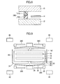
- a wall portion 60 is provided to the substrate 12.
- the wall portion 60 is arranged in the oil 46 as well.
- the wall portion 60 includes a first wall portion 62 and a second wall portion 64.
- the first wall portion 62 is positioned adjacent to (on both sides or one side of) the shutter 14 in a direction orthogonal to the driving direction of the shutter 14 (right-left direction in FIG. 3 ).
- the length of the first wall portion 62 exceeds the length (width) of the shutter 14 in the driving direction.
- the length (width) of the first wall portion 62 is preferred to be equal to or larger than the length (width) of a region in which the shutter 14 is driven to linearly reciprocate. In this manner, no matter where the driven shutter 14 is positioned, the first wall portion 62 is always arranged lateral to the shutter 14.
- the second wall portion 64 is positioned adjacent to (on both sides or one side of) the shutter 14 in the driving direction of the shutter 14 (up-down direction in FIG. 3 ).
- the second wall portion 64 is arranged between a pair of spacers 48.
- a gap is provided between the second wall portion 64 and the spacers 48.
- the second wall portion 64 includes a plurality of divided wall portions 66.
- a gap is provided between the adjacent divided wall portions 66. The oil 46 flows through the gaps, but the flow of the oil 46 is still controlled by the divided wall portions 66.
- the wall portion 60 is provided to prevent the flowing of the oil 46, and hence it is possible to prevent the shutter 14 from being damaged.
- FIG. 6 is a view illustrating a vertical cross-section of a part of the display device including the wall portion.
- the wall portion 60 is provided on the one substrate 12 on which the drive portion 34 is provided.
- the wall portion 60 has a height exceeding that of the shutter 14 in a thickness direction of the shutter 14.
- the wall portion 60 has at least a part positioned lateral to the shutter 14.
- a wall portion 160 may be provided to the other substrate 10 that is different from the one substrate 12 on which the drive portion 34 is provided. Also in this case, the wall portion 160 has a height exceeding that of the shutter 14 in the thickness direction of the shutter 14. That is, the wall portion 160 extends downward from the upper substrate 10 in FIG. 7 , passes the lateral side of the shutter 14, and further extends downward below the shutter 14.
- a wall portion 260 may include a base portion 268 provided on the one substrate 12, and a columnar portion 270 provided on the other substrate 10 so as to be opposed to the base portion 268. Also in this case, the wall portion 260 has a part positioned lateral to the shutter 14. Note that, a gap may be provided between the base portion 268 and the columnar portion 270, or the base portion 268 and the columnar portion 270 may be brought into close contact with each other.
- the wall portion 260 illustrated in FIG. 8 also functions as a spacer of the pair of substrates 10 and 12.
- a wall portion 360 may be arranged at a position closer to the shutter 14 than the spacer 48 (for example, adjacent to the first fixation portion 22). In this case, a part of the drive portion 34 (first fixation portion 22) and the wall portion 360 may be integrated with each other.
- FIG. 10 is a view illustrating a display device according to another embodiment of the present invention.
- a plurality of shutters 414 are arrayed in a plurality of rows and a plurality of columns. Adjacent shutters 414 are arranged so that one of the adjacent shutters 414 is arranged so as to avoid a parallel translation position of the other of the adjacent shutters 414 in at least one of the driving direction and the direction orthogonal to thedrivingdirection.
- the shutters 414 are arrayed in one line in each of the columns (up-down direction in FIG. 10 ), but are arrayed obliquely in the row direction (right-left direction in FIG. 10 ). That is, the shutters 414 are arranged in a staggered manner.
- a wall portion 460 prevents the flowing of the oil 46.
- the wall portion 460 is arranged adjacent to each of the shutters 414 on one side in a direction orthogonal to the driving direction of the shutter 414.
- a spacer 448 is arranged adjacent to the shutter 414 on a side opposite to the one side.
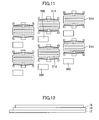
- FIG. 11 is a view illustrating a display device according to further another embodiment of the present invention.
- a plurality of shutters 514 are arrayed in a plurality of rows and a plurality of columns.
- Shutters 514 are arrayed in one line in each of the columns (up-down direction in FIG. 11 ), but are arrayed obliquely in the row direction (right-left direction in FIG. 11 ). That is, the adjacent shutters 514 are arranged so that one of the adjacent shutters 514 is arranged so as to avoid a parallel translation position of the other of the adjacent shutters 514 in at least one of the driving direction and the direction orthogonal to the driving direction.
- a wall portion 560 prevents the flowing of the oil 46.
- the wall portion 560 is arranged adjacent to each of the shutters 514 on both sides in the driving direction of the shutter 514.
- the wall portion 560 also functions as a spacer.
- the present invention is not limited to the above-mentioned embodiments, and various modifications may be made thereto.
- the substrate 12 on which the shutter 14 is formed is arranged on the backlight unit 18 side, but as illustrated in FIG. 12 , there may be employed a structure in which the substrate 10 on which the light shielding film 36 and the fixed aperture 38 are formed is arranged on the backlight unit 18 side.
- the structures described in the embodiments may be replaced by substantially the same structure, a structure which has the same action and effect, or a structure which can achieve the same object.
Abstract

Description
- The present invention relates to a display device.
- A micro-electro-mechanical system (MEMS) display is a display expected to replace a liquid crystal display (see Japanese Patent Application Laid-open No.
2008-197668 - The shutter is arranged in a space surrounded by a sealing member between a pair of light transmissive substrates, and the space is filled with oil. The oil is used to prevent a spring for driving the shutter from sticking, and to reduce a difference in optical refraction index with respect to the light transmissive substrates.
- As one reliability test for the MEMS display, a test of dropping a test ball onto the light transmissive substrate was conducted. As a result, there was observed a phenomenon that the shutter was displaced and the spring disengaged. For comparison, a similar test was performed on an oil-less cell not having oil injected therein, but such damage was not observed. Therefore, the cause of the shutter damage was confirmed to be oil flow.
- The present invention has an object to prevent shutter damage to be caused by oil flow.
- (1) According to an exemplary embodiment of the present invention, there is provided a display device, including: a pair of substrates arranged at an interval; oil filled between the pair of substrates; a shutter arranged in the oil; a drive portion, which is arranged in the oil, for driving the shutter in a predetermined direction (for example, for driving the shutter to linearly reciprocate); and a wall portion provided in the oil and on one of the pair of substrates. The wall portion is positioned adjacent to the shutter in one of the predetermined direction of the shutter and a direction orthogonal to the predetermined direction. The wall portion has a height exceeding a height of the shutter in a thickness direction of the shutter. The wall portion has at least a part positioned lateral to the shutter. According to the present invention, the wall portion is provided to prevent flowing of oil, and hence it is possible to prevent the shutter from being damaged.
- (2) In the display device according to Item (1), the wall portion may have at least a part positioned on at least one of both sides of the shutter in the direction orthogonal to the predetermined direction of the shutter.
- (3) In the display device according to Item (2), at least the part of the wall portion may have a width in the predetermined direction of the shutter, which is larger than a length of the shutter in the predetermined direction.
- (4) In the display device according to any one of Items (1) to (3), the wall portion may have at least a part positioned on at least one of both sides of the shutter in the predetermined direction.
- (5) In the display device according to any one of Items (1) to (4), the wall portion may include a plurality of divided wall portions positioned adjacent to each other at an interval.
- (6) In the display device according to any one of Items (1) to (5), the drive portion may be provided on one of the pair of substrates, and the wall portion may be provided on the one of the pair of substrates on which the drive portion is provided.
- (7) In the display device according to any one of Items (1) to (5), the drive portion may be provided on one of the pair of substrates, and the wall portion may be provided on another of the pair of substrates that is different from the one of the pair of substrates on which the drive portion is provided.
- (8) In the display device according to any one of Items (1) to (5), the drive portion may be provided on one of the pair of substrates, and the wall portion may include: a base portion provided on the one of the pair of substrates; and a columnar portion provided on another of the pair of substrates so as to be opposed to the base portion.
- (9) In the display device according to any one of Items (1) to (8), the shutter may include a plurality of shutters arrayed in a plurality of columns and a plurality of rows, and adjacent shutters of the plurality of shutters may be arranged so that one of the adjacent shutters is arranged so as to avoid a parallel translation position of another of the adjacent shutters in at least one of the predetermined direction and the direction orthogonal to the predetermined direction.
- In the accompanying drawings:
-
FIG. 1 is a side view of a display device according to an embodiment of the present invention; -
FIG. 2 is a plan view of the display device illustrated inFIG. 1 ; -
FIG. 3 is a plan view of a shutter and a drive portion thereof; -
FIG. 4 is a sectional view of a part of the display device including the shutter; -
FIG. 5 is a sectional view of a part of the display device including a spacer; -
FIG. 6 is a view illustrating a vertical cross-section of a part of the display device including a wall portion; -
FIG. 7 is a view illustrating a vertical cross-section of a part of the display device including a modified example of the wall portion; -
FIG. 8 is a view illustrating a vertical cross-section of a part of the display device including another modified example of the wall portion; -
FIG. 9 is a plan view illustrating further another modified example of the wall portion; -
FIG. 10 is a view illustrating a display device according to another embodiment of the present invention; -
FIG. 11 is a view illustrating a display device according to further another embodiment of the present invention; and -
FIG. 12 is a view illustrating a modified example of the display device according to the embodiment of the present invention. - Hereinafter, embodiments of the present invention are described with reference to the drawings.
-
FIG. 1 is a side view of a display device according to the embodiment of the present invention. The display device includes a pair ofsubstrates substrates FIG. 4 ).FIG. 2 is a plan view of the display device illustrated inFIG. 1 . InFIG. 2 , theupper substrate 10 is represented by a virtual line to show the inner structure. As illustrated inFIG. 2 , a plurality of (large number of)shutters 14 are provided on thelower substrate 12. -
FIG. 3 is a plan view of the shutter and a drive portion thereof. Theshutter 14 is a plate which is made of aninorganic material such as semiconductor or a metal, and includes adrive aperture 16. Light is allowed to pass through thedrive aperture 16, and is blocked at a part other than thedrive aperture 16 of theshutter 14. Thedrive aperture 16 has a shape long in one direction. Note that, as illustrated inFIG. 1 , light is supplied from abacklight unit 18 lying under the substrates. - The
shutter 14 is supported by afirst spring 20 to be suspended above the substrate 12 (seeFIG. 4 ). A plurality of (four inFIG. 3 ) firstsprings 20 support theshutter 14. Thefirst spring 20 is fixed to thesubstrate 12 by afirst fixation portion 22. - The
first spring 20 is made of an elastically deformable material, and is arranged so as to be deformable in a direction parallel to the plate surface of theshutter 14. Specifically, thefirst spring 20 includes afirst portion 24 extending in a direction separating from the shutter 14 (direction intersecting (for example, orthogonal to) the length direction of the drive aperture 16), asecond portion 26 extending in a direction along the length direction of thedrive aperture 16 outwardly from a center of thedrive aperture 16 in the length direction, and athird portion 28 further extending in the direction separating from the shutter 14 (direction intersecting (for example, orthogonal to) the length direction of the drive aperture 16). Further, as indicated by the arrows inFIG. 3 , theshutter 14 is supported by thefirst spring 20 so as to be movable in the direction intersecting (for example, orthogonal to) the length direction of thedrive aperture 16. - The
substrate 12 is provided with asecond spring 32 supported by asecond fixation portion 30. Thesecond spring 32 is opposed to thesecond portion 26 of thefirst spring 20 on a side separated from theshutter 14 with respect to thesecond portion 26. When a voltage is applied to thesecond fixation portion 30, due to the electrostatic attractive force caused by the potential difference between thesecond fixation portion 30 and thesecond portion 26 of the thefirst spring 20, thesecond portion 26 is attracted toward thesecond fixation portion 30. When thesecond portion 26 is attracted, theshutter 14 is also attracted via thefirst portion 24 provided integrally with thesecond portion 26. That is, thefirst spring 20 and thesecond spring 32 are provided for constituting adrive portion 34 for driving theshutter 14 to linearly reciprocate (driving theshutter 14 in a predetermined direction). Thedrive portion 34 is also made of an inorganic material such as semiconductor or a metal. -
FIG. 4 is a sectional view of a part of the display device including the shutter. Theupper substrate 10 has alight shielding film 36 formed thereon. A fixedaperture 38 is formed in thelight shielding film 36. The above-mentioneddrive aperture 16 of theshutter 14 and the fixedaperture 38 of thelight shielding film 36 are arranged at positions opposed to each other. Light is allowed to pass when both of the apertures communicate with each other, and light is blocked when the fixedaperture 38 of thelight shielding film 36 is covered due to the movement of theshutter 14. In other words, theshutter 14 is mechanically driven so as to control the passage and blocking of light through the fixedaperture 38 of thelight shielding film 36. Onedrive aperture 16 and one fixedaperture 38 corresponding to each other constitute one pixel, and an image is displayed by a large number of pixels. Therefore, the plurality of (large number of)shutters 14 are provided. Theshutters 14 and thedrive portions 34 thereof are arranged in a display region which displays an image depending on the presence/absence and intensity of light passing through thedrive aperture 16 and the fixedaperture 38. - The pair of
substrates member 40 illustrated inFIG. 2 . The sealingmember 40 is provided in close contact with opposed surfaces of the pair ofsubstrates FIG. 2 , the sealingmember 40 includes anopening 42 and is formed so as to surround a space. Anend seal 44 closes theopening 42 of the sealingmember 40, thereby encapsulating the space surrounded by the sealingmember 40 to form an encapsulation space. - As illustrated in
FIG. 4 , oil 46 (for example, silicone oil) is filled in the encapsulation space. Theshutter 14 and thedrive portion 34 are arranged in theoil 46. Theoil 46 can suppress vibrations caused by the movement of theshutter 14 and thedrive portion 34, and also can prevent sticking of thefirst spring 20 and thesecond spring 32. When thesubstrates oil 46 having a refractive index close to that of glass, through filling of theoil 46, it is possible to reduce light reflection at an interface of the pair ofsubstrates - As illustrated in
FIG. 3 , the display device includes aspacer 48 for maintaining an interval between the pair ofsubstrates FIG. 5 is a sectional view of a part of the display device including the spacer. Thespacer 48 is arranged in theoil 46 as well. As illustrated inFIG. 3 , thespacer 48 is provided offset from theshutter 14 in an oblique direction. Specifically, thespacer 48 is arranged so as to avoid a position offset from theshutter 14 in a driving direction of theshutter 14, and further avoid a position offset in a direction orthogonal to the driving direction. Thespacer 48 may block the flow of theoil 46, but does not block the flow of theoil 46 in a direction most affecting the shutter 14 (driving direction of theshutter 14 or direction orthogonal to the driving direction). - As illustrated in
FIG. 5 , thespacer 48 includes afirst spacer portion 50 provided on theupper substrate 10, and a second spacer portion 52 provided on thelower substrate 12. Thefirst spacer portion 50 is made of a resin. The second spacer portion 52 includes two layers ofresin portions 54 and 56, and aninorganic portion 58 which is made of a semiconductor film or a metal film covering the surfaces of theresin portions 54 and 56. A gap is provided between thefirst spacer portion 50 and the second spacer portion 52, and theoil 46 enters between both the spacer portions. When a force is applied so that thesubstrates first spacer portion 50 and the second spacer portion 52 becomes narrow, and thus theoil 46 therebetween flows. - As illustrated in
FIG. 3 , in addition to thespacer 48, awall portion 60 is provided to thesubstrate 12. Thewall portion 60 is arranged in theoil 46 as well. Thewall portion 60 includes afirst wall portion 62 and asecond wall portion 64. - The
first wall portion 62 is positioned adjacent to (on both sides or one side of) theshutter 14 in a direction orthogonal to the driving direction of the shutter 14 (right-left direction inFIG. 3 ). The length of the first wall portion 62 (width of thefirst wall portion 62 in the driving direction of the shutter 14) exceeds the length (width) of theshutter 14 in the driving direction. Further, the length (width) of thefirst wall portion 62 is preferred to be equal to or larger than the length (width) of a region in which theshutter 14 is driven to linearly reciprocate. In this manner, no matter where the drivenshutter 14 is positioned, thefirst wall portion 62 is always arranged lateral to theshutter 14. - The
second wall portion 64 is positioned adjacent to (on both sides or one side of) theshutter 14 in the driving direction of the shutter 14 (up-down direction inFIG. 3 ). Thesecond wall portion 64 is arranged between a pair ofspacers 48. A gap is provided between thesecond wall portion 64 and thespacers 48. Further, thesecond wall portion 64 includes a plurality of dividedwall portions 66. A gap is provided between the adjacent dividedwall portions 66. Theoil 46 flows through the gaps, but the flow of theoil 46 is still controlled by the dividedwall portions 66. - According to this embodiment, the
wall portion 60 is provided to prevent the flowing of theoil 46, and hence it is possible to prevent theshutter 14 from being damaged. -
FIG. 6 is a view illustrating a vertical cross-section of a part of the display device including the wall portion. Thewall portion 60 is provided on the onesubstrate 12 on which thedrive portion 34 is provided. Thewall portion 60 has a height exceeding that of theshutter 14 in a thickness direction of theshutter 14. Thewall portion 60 has at least a part positioned lateral to theshutter 14. - Alternatively, as a modified example, as illustrated in
FIG. 7 , awall portion 160 may be provided to theother substrate 10 that is different from the onesubstrate 12 on which thedrive portion 34 is provided. Also in this case, thewall portion 160 has a height exceeding that of theshutter 14 in the thickness direction of theshutter 14. That is, thewall portion 160 extends downward from theupper substrate 10 inFIG. 7 , passes the lateral side of theshutter 14, and further extends downward below theshutter 14. - Alternatively, as another modified example, as illustrated in
FIG. 8 , awall portion 260 may include abase portion 268 provided on the onesubstrate 12, and acolumnar portion 270 provided on theother substrate 10 so as to be opposed to thebase portion 268. Also in this case, thewall portion 260 has a part positioned lateral to theshutter 14. Note that, a gap may be provided between thebase portion 268 and thecolumnar portion 270, or thebase portion 268 and thecolumnar portion 270 may be brought into close contact with each other. Thewall portion 260 illustrated inFIG. 8 also functions as a spacer of the pair ofsubstrates - As further another modified example, as illustrated in
FIG. 9 , awall portion 360 may be arranged at a position closer to theshutter 14 than the spacer 48 (for example, adjacent to the first fixation portion 22). In this case, a part of the drive portion 34 (first fixation portion 22) and thewall portion 360 may be integrated with each other. -
FIG. 10 is a view illustrating a display device according to another embodiment of the present invention. In this embodiment, a plurality ofshutters 414 are arrayed in a plurality of rows and a plurality of columns.Adjacent shutters 414 are arranged so that one of theadjacent shutters 414 is arranged so as to avoid a parallel translation position of the other of theadjacent shutters 414 in at least one of the driving direction and the direction orthogonal to thedrivingdirection. Specifically, theshutters 414 are arrayed in one line in each of the columns (up-down direction inFIG. 10 ), but are arrayed obliquely in the row direction (right-left direction inFIG. 10 ). That is, theshutters 414 are arranged in a staggered manner. - Also in this embodiment, a
wall portion 460 prevents the flowing of theoil 46. Thewall portion 460 is arranged adjacent to each of theshutters 414 on one side in a direction orthogonal to the driving direction of theshutter 414. Aspacer 448 is arranged adjacent to theshutter 414 on a side opposite to the one side. -
FIG. 11 is a view illustrating a display device according to further another embodiment of the present invention. In this embodiment, a plurality ofshutters 514 are arrayed in a plurality of rows and a plurality of columns.Shutters 514 are arrayed in one line in each of the columns (up-down direction inFIG. 11 ), but are arrayed obliquely in the row direction (right-left direction inFIG. 11 ). That is, theadjacent shutters 514 are arranged so that one of theadjacent shutters 514 is arranged so as to avoid a parallel translation position of the other of theadjacent shutters 514 in at least one of the driving direction and the direction orthogonal to the driving direction. - Also in this embodiment, a
wall portion 560 prevents the flowing of theoil 46. Thewall portion 560 is arranged adjacent to each of theshutters 514 on both sides in the driving direction of theshutter 514. Thewall portion 560 also functions as a spacer. - The present invention is not limited to the above-mentioned embodiments, and various modifications may be made thereto. For example, in the above-mentioned embodiments, the
substrate 12 on which theshutter 14 is formed is arranged on thebacklight unit 18 side, but as illustrated inFIG. 12 , there may be employed a structure in which thesubstrate 10 on which thelight shielding film 36 and the fixedaperture 38 are formed is arranged on thebacklight unit 18 side. Further, the structures described in the embodiments may be replaced by substantially the same structure, a structure which has the same action and effect, or a structure which can achieve the same object.
Claims (11)
- A display device, comprising:a pair of substrates (10, 12) arranged at an interval;oil filled between the pair of substrates (10, 12);a shutter (14) arranged in the oil (46);a drive portion (34), which is arranged in the oil (46), for driving the shutter (14) in a predetermined direction; anda wall portion (60) provided in the oil (46) and on one of the pair of substrates (10, 12),wherein the wall portion (60) is positioned adjacent to the shutter (14) in one of the predetermined direction of the shutter (14) and a direction orthogonal to the predetermined direction,wherein the wall portion (60) has a height exceeding a height of the shutter (14) in a thickness direction of the shutter (14), andwherein the wall portion (60) has at least a part positioned lateral to the shutter (14).
- The display device according to claim 1, wherein the wall portion (60) has at least a part positioned on at least one of both sides of the shutter (14) in the direction orthogonal to the predetermined direction.
- The display device according to claim 2, wherein at least the part of the wall portion (60) has a width in the predetermined direction of the shutter (14), which is larger than a length of the shutter (14) in the predetermined direction.
- The display device according to any one of claims 1 to 3, wherein the wall portion (60) has at least a part positioned on at least one of both sides of the shutter (14) in the predetermined direction.
- The display device according to any one of claims 1 to 4, wherein the wall portion (60) comprises a plurality of divided wall portions (66) positioned adjacent to each other at an interval.
- The display device according to any one of claims 1 to 5,
wherein the drive portion (34) is provided on one (12) of the pair of substrates (10, 12), and
wherein the wall portion (60) is provided on the one (12) of the pair of substrates (10, 12) on which the drive portion (34) is provided. - The display device according to any one of claims 1 to 5,
wherein the drive portion (34) is provided on one (12) of the pair of substrates (10, 12), and
wherein the wall portion (160) is provided on another (10) of the pair of substrates (10, 12) that is different from the one (12) of the pair of substrates (10, 12) on which the drive portion (34) is provided. - The display device according to any one of claims 1 to 5,
wherein the drive portion (34) is provided on one (12) of the pair of substrates (10, 12), and
wherein the wall portion (260) comprises:a base portion (268) provided on the one (12) of the pair of substrates (10, 12); anda columnar portion (270) provided on another (10) of the pair of substrates (10, 12) so as to be opposed to the base portion. - The display device according to any one of claims 6 to 8, further comprising a backlight unit (18) provided opposed to the pair of substrates (10, 12),
wherein the one (10) of the pair of substrates (10, 12) is arranged on a side opposite to the backlight unit (18). - The display device according to any one of claims 6 to 8, further comprising a backlight unit provided opposed to the pair of substrates (10, 12),
wherein the one (12) of the pair of substrates (10, 12) is arranged on the backlight unit side. - The display device according to any one of claims 1 to 10,
wherein the shutter comprises a plurality of shutters (514) arrayed in a plurality of columns and a plurality of rows, and
wherein adjacent shutters (514) of the plurality of shutters (514) are arranged so that one of the adjacent shutters (514) is arranged so as to avoid a parallel translation position of another of the adjacent shutters (514) in at least one of the predetermined direction and the direction orthogonal to the predetermined direction.
Applications Claiming Priority (1)
| Application Number | Priority Date | Filing Date | Title |
|---|---|---|---|
| JP2011110513A JP2012242495A (en) | 2011-05-17 | 2011-05-17 | Display device |
Publications (1)
| Publication Number | Publication Date |
|---|---|
| EP2525246A1 true EP2525246A1 (en) | 2012-11-21 |
Family
ID=46149200
Family Applications (1)
| Application Number | Title | Priority Date | Filing Date |
|---|---|---|---|
| EP12168092A Withdrawn EP2525246A1 (en) | 2011-05-17 | 2012-05-15 | Display device |
Country Status (6)
| Country | Link |
|---|---|
| US (1) | US8941909B2 (en) |
| EP (1) | EP2525246A1 (en) |
| JP (1) | JP2012242495A (en) |
| KR (3) | KR101447727B1 (en) |
| CN (1) | CN102809811B (en) |
| TW (1) | TWI479192B (en) |
Cited By (2)
| Publication number | Priority date | Publication date | Assignee | Title |
|---|---|---|---|---|
| WO2014074515A1 (en) * | 2012-11-06 | 2014-05-15 | Pixtronix, Inc. | Display device and manufacturing method of same |
| WO2014093169A1 (en) * | 2012-12-13 | 2014-06-19 | Pixtronix, Inc. | Display with light modulating pixels organized in off-axis arrangement |
Families Citing this family (4)
| Publication number | Priority date | Publication date | Assignee | Title |
|---|---|---|---|---|
| JP5856758B2 (en) * | 2011-05-23 | 2016-02-10 | ピクストロニクス,インコーポレイテッド | Display device and manufacturing method thereof |
| JP2013020105A (en) * | 2011-07-12 | 2013-01-31 | Japan Display East Co Ltd | Display device |
| US20140078154A1 (en) * | 2012-09-14 | 2014-03-20 | Pixtronix, Inc. | Display apparatus with multi-height spacers |
| US9897796B2 (en) | 2014-04-18 | 2018-02-20 | Snaptrack, Inc. | Encapsulated spacers for electromechanical systems display apparatus |
Citations (5)
| Publication number | Priority date | Publication date | Assignee | Title |
|---|---|---|---|---|
| JP2008197668A (en) | 2005-02-23 | 2008-08-28 | Pixtronix Inc | Display methods and apparatus |
| EP2103982A1 (en) * | 2007-01-10 | 2009-09-23 | Sony Corporation | Liquid device, liquid device manufacturing apparatus and method, and image display device |
| US20100027100A1 (en) * | 2008-08-04 | 2010-02-04 | Pixtronix, Inc. | Display with controlled formation of bubbles |
| US20100245408A1 (en) * | 2007-12-19 | 2010-09-30 | Toshiki Matsuoka | Display device and electric apparatus using the same |
| US7911681B2 (en) * | 2005-07-29 | 2011-03-22 | Dai Nippon Printing Co., Ltd. | Display device, its manufacturing method, and display medium |
Family Cites Families (10)
| Publication number | Priority date | Publication date | Assignee | Title |
|---|---|---|---|---|
| JP3799092B2 (en) * | 1995-12-29 | 2006-07-19 | アジレント・テクノロジーズ・インク | Light modulation device and display device |
| US7573547B2 (en) | 2004-09-27 | 2009-08-11 | Idc, Llc | System and method for protecting micro-structure of display array using spacers in gap within display device |
| EP2116885B1 (en) * | 2005-02-23 | 2014-07-23 | Pixtronix, Inc. | Display methods and apparatus |
| JP2006337858A (en) * | 2005-06-03 | 2006-12-14 | Fujifilm Holdings Corp | Optical modulation element array |
| CN100538492C (en) * | 2005-07-29 | 2009-09-09 | 大日本印刷株式会社 | Display device, its manufacture method and display medium |
| JP2008170632A (en) | 2007-01-10 | 2008-07-24 | Sony Corp | Liquid device, and device and method for manufacturing liquid device |
| EP2264507A3 (en) * | 2007-01-19 | 2011-07-20 | Pixtronix Inc. | A display apparatus |
| KR101534011B1 (en) * | 2008-11-20 | 2015-07-06 | 삼성디스플레이 주식회사 | Plat panel display and manufacturing method thereof |
| KR101571777B1 (en) | 2009-03-06 | 2015-11-26 | 삼성디스플레이 주식회사 | Light guide unit and display apparatus having the same |
| KR101701234B1 (en) | 2010-07-30 | 2017-02-02 | 삼성디스플레이 주식회사 | Display panel, method of driving the display panel and display device performing the method |
-
2011
- 2011-05-17 JP JP2011110513A patent/JP2012242495A/en active Pending
-
2012
- 2012-05-15 EP EP12168092A patent/EP2525246A1/en not_active Withdrawn
- 2012-05-15 TW TW101117260A patent/TWI479192B/en active
- 2012-05-16 US US13/472,600 patent/US8941909B2/en not_active Expired - Fee Related
- 2012-05-16 KR KR1020120051913A patent/KR101447727B1/en not_active IP Right Cessation
- 2012-05-16 CN CN201210160898.XA patent/CN102809811B/en not_active Expired - Fee Related
-
2014
- 2014-06-26 KR KR1020140078974A patent/KR20140089500A/en not_active IP Right Cessation
-
2015
- 2015-05-28 KR KR1020150075270A patent/KR20150067108A/en not_active Application Discontinuation
Patent Citations (5)
| Publication number | Priority date | Publication date | Assignee | Title |
|---|---|---|---|---|
| JP2008197668A (en) | 2005-02-23 | 2008-08-28 | Pixtronix Inc | Display methods and apparatus |
| US7911681B2 (en) * | 2005-07-29 | 2011-03-22 | Dai Nippon Printing Co., Ltd. | Display device, its manufacturing method, and display medium |
| EP2103982A1 (en) * | 2007-01-10 | 2009-09-23 | Sony Corporation | Liquid device, liquid device manufacturing apparatus and method, and image display device |
| US20100245408A1 (en) * | 2007-12-19 | 2010-09-30 | Toshiki Matsuoka | Display device and electric apparatus using the same |
| US20100027100A1 (en) * | 2008-08-04 | 2010-02-04 | Pixtronix, Inc. | Display with controlled formation of bubbles |
Cited By (2)
| Publication number | Priority date | Publication date | Assignee | Title |
|---|---|---|---|---|
| WO2014074515A1 (en) * | 2012-11-06 | 2014-05-15 | Pixtronix, Inc. | Display device and manufacturing method of same |
| WO2014093169A1 (en) * | 2012-12-13 | 2014-06-19 | Pixtronix, Inc. | Display with light modulating pixels organized in off-axis arrangement |
Also Published As
| Publication number | Publication date |
|---|---|
| CN102809811B (en) | 2015-09-16 |
| US20120293851A1 (en) | 2012-11-22 |
| KR101447727B1 (en) | 2014-10-06 |
| CN102809811A (en) | 2012-12-05 |
| JP2012242495A (en) | 2012-12-10 |
| KR20140089500A (en) | 2014-07-15 |
| TWI479192B (en) | 2015-04-01 |
| TW201300830A (en) | 2013-01-01 |
| KR20150067108A (en) | 2015-06-17 |
| US8941909B2 (en) | 2015-01-27 |
| KR20120128574A (en) | 2012-11-27 |
Similar Documents
| Publication | Publication Date | Title |
|---|---|---|
| US8941909B2 (en) | Display device | |
| US9250437B2 (en) | Display device | |
| US9134531B2 (en) | Display device and method for manufacturing the same | |
| JP2012248293A (en) | Backlight and display device | |
| EP2523031A1 (en) | Display device | |
| KR101343546B1 (en) | Display apparatus | |
| US20130100091A1 (en) | Display device | |
| US20120307192A1 (en) | Display device | |
| US8730550B2 (en) | Display device | |
| JP2014077913A (en) | Display device | |
| JP2014077912A (en) | Display device and method for manufacturing the same | |
| KR20120127291A (en) | Display device |
Legal Events
| Date | Code | Title | Description |
|---|---|---|---|
| PUAI | Public reference made under article 153(3) epc to a published international application that has entered the european phase |
Free format text: ORIGINAL CODE: 0009012 |
|
| AK | Designated contracting states |
Kind code of ref document: A1 Designated state(s): AL AT BE BG CH CY CZ DE DK EE ES FI FR GB GR HR HU IE IS IT LI LT LU LV MC MK MT NL NO PL PT RO RS SE SI SK SM TR |
|
| AX | Request for extension of the european patent |
Extension state: BA ME |
|
| 17P | Request for examination filed |
Effective date: 20121130 |
|
| RAP1 | Party data changed (applicant data changed or rights of an application transferred) |
Owner name: JAPAN DISPLAY INC. |
|
| RAP1 | Party data changed (applicant data changed or rights of an application transferred) |
Owner name: PIXTRONIX, INC. |
|
| 17Q | First examination report despatched |
Effective date: 20151215 |
|
| STAA | Information on the status of an ep patent application or granted ep patent |
Free format text: STATUS: THE APPLICATION IS DEEMED TO BE WITHDRAWN |
|
| 18D | Application deemed to be withdrawn |
Effective date: 20160426 |