EP2525162A1 - A solar thermal absorber material - Google Patents
A solar thermal absorber material Download PDFInfo
- Publication number
- EP2525162A1 EP2525162A1 EP11166762A EP11166762A EP2525162A1 EP 2525162 A1 EP2525162 A1 EP 2525162A1 EP 11166762 A EP11166762 A EP 11166762A EP 11166762 A EP11166762 A EP 11166762A EP 2525162 A1 EP2525162 A1 EP 2525162A1
- Authority
- EP
- European Patent Office
- Prior art keywords
- layer
- thickness
- sio
- solar thermal
- multilayer structure
- Prior art date
- Legal status (The legal status is an assumption and is not a legal conclusion. Google has not performed a legal analysis and makes no representation as to the accuracy of the status listed.)
- Granted
Links
- 239000006096 absorbing agent Substances 0.000 title claims abstract description 72
- 239000000463 material Substances 0.000 title claims abstract description 72
- VYPSYNLAJGMNEJ-UHFFFAOYSA-N Silicium dioxide Chemical compound O=[Si]=O VYPSYNLAJGMNEJ-UHFFFAOYSA-N 0.000 claims abstract description 245
- PNEYBMLMFCGWSK-UHFFFAOYSA-N aluminium oxide Inorganic materials [O-2].[O-2].[O-2].[Al+3].[Al+3] PNEYBMLMFCGWSK-UHFFFAOYSA-N 0.000 claims abstract description 225
- 229910052681 coesite Inorganic materials 0.000 claims abstract description 127
- 229910052906 cristobalite Inorganic materials 0.000 claims abstract description 127
- 229910052682 stishovite Inorganic materials 0.000 claims abstract description 127
- 229910052905 tridymite Inorganic materials 0.000 claims abstract description 127
- 239000000377 silicon dioxide Substances 0.000 claims abstract description 118
- 239000000758 substrate Substances 0.000 claims abstract description 45
- 229910052593 corundum Inorganic materials 0.000 claims abstract 21
- 229910001845 yogo sapphire Inorganic materials 0.000 claims abstract 21
- 239000010949 copper Substances 0.000 claims description 64
- 229910001220 stainless steel Inorganic materials 0.000 claims description 64
- 239000010935 stainless steel Substances 0.000 claims description 64
- RYGMFSIKBFXOCR-UHFFFAOYSA-N Copper Chemical compound [Cu] RYGMFSIKBFXOCR-UHFFFAOYSA-N 0.000 claims description 10
- 229910052802 copper Inorganic materials 0.000 claims description 10
- 229910052782 aluminium Inorganic materials 0.000 claims description 7
- 239000004411 aluminium Substances 0.000 claims description 7
- XAGFODPZIPBFFR-UHFFFAOYSA-N aluminium Chemical compound [Al] XAGFODPZIPBFFR-UHFFFAOYSA-N 0.000 claims description 7
- ZOKXTWBITQBERF-UHFFFAOYSA-N Molybdenum Chemical compound [Mo] ZOKXTWBITQBERF-UHFFFAOYSA-N 0.000 claims description 6
- 229910052750 molybdenum Inorganic materials 0.000 claims description 6
- 239000011733 molybdenum Substances 0.000 claims description 6
- 230000007423 decrease Effects 0.000 claims description 3
- 238000009833 condensation Methods 0.000 description 25
- 230000005494 condensation Effects 0.000 description 25
- 239000013074 reference sample Substances 0.000 description 19
- 238000012360 testing method Methods 0.000 description 19
- 230000003287 optical effect Effects 0.000 description 18
- 230000007797 corrosion Effects 0.000 description 14
- 238000005260 corrosion Methods 0.000 description 14
- 239000000523 sample Substances 0.000 description 11
- 239000011248 coating agent Substances 0.000 description 9
- 238000000576 coating method Methods 0.000 description 9
- 238000004088 simulation Methods 0.000 description 9
- 229910052751 metal Inorganic materials 0.000 description 6
- 239000002184 metal Substances 0.000 description 6
- 238000010438 heat treatment Methods 0.000 description 5
- 238000010586 diagram Methods 0.000 description 4
- XLYOFNOQVPJJNP-UHFFFAOYSA-N water Substances O XLYOFNOQVPJJNP-UHFFFAOYSA-N 0.000 description 4
- 238000012512 characterization method Methods 0.000 description 3
- 230000007547 defect Effects 0.000 description 3
- 230000000694 effects Effects 0.000 description 3
- 239000012530 fluid Substances 0.000 description 3
- 238000005240 physical vapour deposition Methods 0.000 description 3
- 230000008901 benefit Effects 0.000 description 2
- 230000001427 coherent effect Effects 0.000 description 2
- 230000006866 deterioration Effects 0.000 description 2
- 150000004679 hydroxides Chemical class 0.000 description 2
- 230000007774 longterm Effects 0.000 description 2
- TWNQGVIAIRXVLR-UHFFFAOYSA-N oxo(oxoalumanyloxy)alumane Chemical compound O=[Al]O[Al]=O TWNQGVIAIRXVLR-UHFFFAOYSA-N 0.000 description 2
- 230000008092 positive effect Effects 0.000 description 2
- 230000005855 radiation Effects 0.000 description 2
- 230000003595 spectral effect Effects 0.000 description 2
- 238000001228 spectrum Methods 0.000 description 2
- 239000010409 thin film Substances 0.000 description 2
- 238000005033 Fourier transform infrared spectroscopy Methods 0.000 description 1
- 229910000831 Steel Inorganic materials 0.000 description 1
- 230000003542 behavioural effect Effects 0.000 description 1
- 238000009835 boiling Methods 0.000 description 1
- 238000004590 computer program Methods 0.000 description 1
- 238000011156 evaluation Methods 0.000 description 1
- 230000001747 exhibiting effect Effects 0.000 description 1
- 238000002474 experimental method Methods 0.000 description 1
- 238000005259 measurement Methods 0.000 description 1
- 239000007769 metal material Substances 0.000 description 1
- 238000000034 method Methods 0.000 description 1
- 230000000149 penetrating effect Effects 0.000 description 1
- 230000035515 penetration Effects 0.000 description 1
- 230000001681 protective effect Effects 0.000 description 1
- 239000012925 reference material Substances 0.000 description 1
- 239000010959 steel Substances 0.000 description 1
- 239000000126 substance Substances 0.000 description 1
- 239000008399 tap water Substances 0.000 description 1
- 235000020679 tap water Nutrition 0.000 description 1
Images




Classifications
-
- F—MECHANICAL ENGINEERING; LIGHTING; HEATING; WEAPONS; BLASTING
- F24—HEATING; RANGES; VENTILATING
- F24S—SOLAR HEAT COLLECTORS; SOLAR HEAT SYSTEMS
- F24S70/00—Details of absorbing elements
- F24S70/20—Details of absorbing elements characterised by absorbing coatings; characterised by surface treatment for increasing absorption
- F24S70/25—Coatings made of metallic material
-
- F—MECHANICAL ENGINEERING; LIGHTING; HEATING; WEAPONS; BLASTING
- F24—HEATING; RANGES; VENTILATING
- F24S—SOLAR HEAT COLLECTORS; SOLAR HEAT SYSTEMS
- F24S70/00—Details of absorbing elements
- F24S70/20—Details of absorbing elements characterised by absorbing coatings; characterised by surface treatment for increasing absorption
- F24S70/225—Details of absorbing elements characterised by absorbing coatings; characterised by surface treatment for increasing absorption for spectrally selective absorption
-
- Y—GENERAL TAGGING OF NEW TECHNOLOGICAL DEVELOPMENTS; GENERAL TAGGING OF CROSS-SECTIONAL TECHNOLOGIES SPANNING OVER SEVERAL SECTIONS OF THE IPC; TECHNICAL SUBJECTS COVERED BY FORMER USPC CROSS-REFERENCE ART COLLECTIONS [XRACs] AND DIGESTS
- Y02—TECHNOLOGIES OR APPLICATIONS FOR MITIGATION OR ADAPTATION AGAINST CLIMATE CHANGE
- Y02B—CLIMATE CHANGE MITIGATION TECHNOLOGIES RELATED TO BUILDINGS, e.g. HOUSING, HOUSE APPLIANCES OR RELATED END-USER APPLICATIONS
- Y02B10/00—Integration of renewable energy sources in buildings
- Y02B10/20—Solar thermal
-
- Y—GENERAL TAGGING OF NEW TECHNOLOGICAL DEVELOPMENTS; GENERAL TAGGING OF CROSS-SECTIONAL TECHNOLOGIES SPANNING OVER SEVERAL SECTIONS OF THE IPC; TECHNICAL SUBJECTS COVERED BY FORMER USPC CROSS-REFERENCE ART COLLECTIONS [XRACs] AND DIGESTS
- Y02—TECHNOLOGIES OR APPLICATIONS FOR MITIGATION OR ADAPTATION AGAINST CLIMATE CHANGE
- Y02E—REDUCTION OF GREENHOUSE GAS [GHG] EMISSIONS, RELATED TO ENERGY GENERATION, TRANSMISSION OR DISTRIBUTION
- Y02E10/00—Energy generation through renewable energy sources
- Y02E10/40—Solar thermal energy, e.g. solar towers
Definitions
- the present invention relates to a solar thermal absorber material according to the preamble of claim 1.
- Solar thermal absorbers are typically used in household applications for converting sunlight into heat. These absorbers are usually referred to as "low temperature flat plate absorbers" as the typical operating temperature is below 400°C.
- a solar thermal absorber typically comprises a plate-like substrate of heat conductive metal such as copper, steel or aluminium. Fluid conducting tubes are attached to one side of the metallic plate, the inner side thereof, whereas the outer side of the plate is coated with a thin dark surface coating. The properties of the dark coating are such that the coating reflects very little of incident sunlight. Therefore, when the dark surface coating is exposed to sunlight it absorbs heat from the sunlight and thereby heats the metallic plate. The heat is transferred from the metallic plate to a fluid, for example water, which circulates in the tubes on the rear side of the plate. The heated fluid can be used in various household heating applications, such as heating of tap water.
- solar thermal absorbers of this type are enclosed in box-like protective housings comprising a transparent window and are arranged on the roofs of buildings.
- the dark coating is a multilayer structure having layers of Al 2 O 3 , SiO 2 , Mo, SiO 2 , Mo, SiO 2 in order from the substrate.
- the multilayer structure is applied onto a metallic strip substrate of copper, stainless steel or aluminium.
- this known type of solar thermal absorber material has occasionally exhibited low resistance against high temperatures and moisture induced corrosion.
- moisture induced corrosion has occurred on solar absorbers based on copper substrate having the above mentioned multilayer structure.
- Solar absorbers of the above type that are based on aluminium substrates have somewhat better corrosion resistance than the ones comprising a copper substrate but does not have satisfactory heat resistance. Therefore, when the above types of solar absorbers are exposed for long periods to warm and humid weather conditions the properties of the absorbers tend to deteriorate, which shortens the service life of the absorbers.
- a solar thermal absorber material comprising:
- the inventive solar thermal absorber material has very high resistance to moisture induced corrosion and high temperatures.
- the "heat resistance" of a solar absorber material is in general the ability of the material to withstand high temperatures without losing its heat retaining capacity or having the layer structure crack or delaminating from the substrate.
- the resistance to heat, and also to some extent the resistance to moisture-induced corrosion is believed to be influenced by the fact that the alternating layers of aluminium oxide (Al 2 O 3 ) and molybdenum (Mo) molybdenum have similar thermal expansion coefficients.
- the layers of Al 2 O 3 and Mo expand uniformly and substantially no strain or tension forms in the layer structure which otherwise would have caused the layer structure to break and to delaminate from the substrate.
- Corrosion in solar absorbers is generally caused by moisture from the atmosphere around the solar absorber that penetrates through the multilayer structure down to the metallic substrate and form oxides/hydroxides thereon.
- the oxides/hydroxides deteriorate the adhesion between the multilayer structure and the substrate which causes the multilayer structure to delaminate from the substrate.
- the high resistance to corrosion in the inventive material is believed to be caused by the following factors:
- the outermost layer of the inventive multilayer structure is a layer of SiO 2 . It is believed that the layer of SiO 2 absorbs moisture and therefore prevents moisture from penetrating through the underlying layers of Al 2 O 3 and Mo to the surface of the metallic substrate. Even though the thermal expansion coefficient of SiO 2 is different from the thermal expansion coefficient of Mo and Al 2 O 3 tensions does not build up in the multilayer structure when the structure is heated since the SiO 2 layer is the outermost layer.
- the outermost SiO 2 layer is applied directly onto an underlying Al 2 O 3 layer.
- the reason therefore is that SiO 2 and Al 2 O 3 have similar refraction index. Therefore the optical properties of the multilayer structure, i.e. the ratio of absorptance/emittance are not negatively influenced to a significant extent by the SiO 2 layer. This could otherwise have been the case if the SiO 2 layer was applied onto another layer than Al 2 O 3 , for instance Mo.
- the multilayer structure defined above comprises:
- the multilayer structure has the following configuration, preferably with layer thicknesses as indicated:
- the described inventive multilayer structure comprises a large number of layers, in total five alternating layers of Al 2 O 3 and Mo and the sixth layer of SiO 2 .
- the high number of layers has a positive effect on the corrosion resistance for the following reason:
- the middlemost Al 2 O 3 layer could be formed by two individual Al 2 O 3 layers, which are applied next to each other.
- the effect thereof is that a large number of layers are achieved in the multilayer structure which provides for good protection against moisture penetration.
- the two adjacent Al 2 O 3 layers only constitute one Al 2 O 3 layer and do therefore not alter the optical properties of the solar thermal material.
- the multilayer structure has the following configuration, preferably with layer thicknesses as indicated:
- the thicknesses of the SiO 2 layer and the underlying Al 2 O 3 layer it is preferred to adapt the thicknesses of the SiO 2 layer and the underlying Al 2 O 3 layer to each other.
- the refraction indexes of Al 2 O 3 and SiO 2 are similar. However, for all wavelengths the refraction index of Al 2 O 3 is slightly higher than that of SiO 2 .
- the SiO 2 layer should preferably be thicker than the Al 2 O 3 layer. Since the specific refraction indexes of Al 2 O 3 and SiO 2 varies with the wavelength, the precise relationship between thicknesses of the layers has to be determined by the skilled person. For example if the SiO 2 layer has a thickness of 50 nm, the underlying Al 2 O 3 layer should have a thickness of 45 nm for maintaining the desired optical properties of the solar thermal absorber material.
- the multilayer structure In order to achieve very good corrosion resistance, thick layers could be provided in the multilayer structure.
- the maximum thickness of the layers should however be limited in order to prevent that thermal expansion cause tension and strain in the multilayer structure.
- the optical properties, i.e absorptance and emittance, will also deteriorate if the total thickness of the layer structure become too large. If the total thickness of the multilayer structure exceeds 300 nm less light will be reflected from the substrate back into the multilayer structure and therefore the emittance will increase and the absorptance decrease.
- the layers or some of the layers in the inventive multilayer structure could be made very thin.
- the advantage thereof is that a good compromise between absorptance and emittance is obtained.
- it is difficult to achieve very thin coherent layers and the minimum thickness of the layers should therefore be limited in order to secure that all layers of the inventive multilayer structure are intact and fully closed coalesced thin films.
- the layers in the inventive multilayer structure may have the following thicknesses:
- a solar thermal absorber material comprising this multilayer structure has a robust coherent multilayer structure which provides for good corrosion resistance and good thermal stability.
- the thickness of the Mo layers in the multilayer structure may be selected such that the first Mo layer is twice as thick as the second Mo layer. Thereby a gradient having a low metal fraction towards the surface is obtained in the layer structure. It is preferred to have a metal gradient through the layer structure for the following reason:
- the solar absorber material shall absorb as much solar light as possible and it is therefore preferred that it in total contains a high fraction of metal. However, close to the surface of the solar absorber the fraction of metal shall be low in order to not influence the refraction index of the layer structure.
- the thicknesses of the layers according to this alternative are selected such that:
- the sixth layer of Al 2 O 3 has a thickness of 45 nm.
- the metallic substrate of the inventive solar thermal absorber is preferably selected from copper strip, aluminium strip or stainless steel strip. Such materials have good thermal conductivity and are therefore suitable for use in solar thermal absorbers. Copper and aluminium strip further exhibits adequate reflectance property which is essential for providing low emittance properties in the inventive solar absorber material.
- FIG. 1 shows the inventive solar thermal absorber material according to a preferred embodiment.
- the solar thermal absorber material 10 comprises a substrate 20 which is made of strip of metallic material, preferably copper, aluminium or stainless steel, for example of the sort 15R10.
- the substrate 20 may have a thickness of 0,1-0,4 mm. and its length and width are adapted for the actual application.
- a multilayer structure 30 is applied onto the substrate.
- the multilayer structure has the following configuration: closest to the substrate is a layer 100 of aluminium oxide (Al 2 O 3 ) thereafter a second layer 200 of Molybdenum (Mo) onto which a third and a fourth layer 300, 400 of Al 2 O 3 are applied. Thereafter the multilayer comprises a fifth layer 500 of Mo, a sixth layer 600 of Al 2 O 3 and a seventh 700, outermost layer of SiO 2 .
- the inventive solar thermal absorber material is manufactured by coating a strip material with layers of Al 2 O 3 , Mo and SiO 2 using physical vapour deposition (PVD) in a continuous roll-to-roll process.
- PVD physical vapour deposition
- the surface of the strip material is ion-etched prior to coating in order to provide good adhesion between the multilayer structure and the surface of the strip material.
- the thicknesses of the individual layers in the inventive solar absorber material should be: layer 100 of Al 2 O 3 : 10-240 nm; layer 200 of Mo: 8-120 nm; layer 300 of Al 2 O 3 : 25-50 nm; layer 400 of Al 2 O 3 : 25-50; layer 500 of Mo: 3-60; layer 600 of Al 2 O 3 : 15-45 nm; layer 700 of SiO 2 : 10-50 nm.
- each individual layer should be selected to be within the stated intervals such that the ratio of absorptance/emittance of the solar thermal absorber material is ⁇ 90%/ ⁇ 10% for the selected substrate.
- the ratio between the absorptance/emittance of the solar absorber is a measure on the thermal efficiency of the solar absorber. It is desired to have as high absorptance as possible since as much sunlight as possible shall be absorbed and transferred as heat to the substrate. However in operation, the solar absorber heats up and start to radiate heat. The radiated heat is measured as emittance and can be considered a heat loss from the solar absorber. It is generally accepted that an efficient commercial solar absorber should have an absorptance/emittance ratio of ⁇ 90%/ ⁇ 10% at its operation temperature. However, an thermal solar absorber having an absorptance/emittance ratio of ⁇ 80%/ ⁇ 20% is also fully functional.
- the ratio of absorptance/emittance is influenced by the material in the individual layers and the infra-red properties of the substrate. For example a high fraction of metal in the layer structure has a positive effect on the absorptance. Although no explanation can be given it is further believed that the thicknesses of the individual layers also are of importance for the absorptance/emittance ratio of the solar absorber material.
- the individual layer thicknesses of the inventive solar absorber material according to the above described embodiment were determined from simulations performed using the computer program TS-Calc Thinfilm by Software Specta Inc. In the simulation an initial layer structure was entered in the program. The initial layer structure had the thicknesses:
- Table 1 shows the results of the simulation. Table 1: Results from simulation in TS-Calc on seven layer structure Layer 1 Layer 2 Layer 3/4 Layer 5 Layer 6 Layer 7 Al 2 O 3 Mo Al 2 O 3 / Al 2 O 3 Mo Al 2 O 3 SiO 2 Absorptance/ Emittance 240 20 50 10 45 50 ⁇ 90%/ ⁇ 10% 10 20 50 10 45 50 ⁇ 90%/ ⁇ 10% 60 120 50 10 45 50 ⁇ 90%/ ⁇ 10% 60 8 50 10 45 50 ⁇ 90%/ ⁇ 10% 60 20 105 10 45 50 ⁇ 90%/ ⁇ 10% 60 20 25 10 45 50 ⁇ 90%/ ⁇ 10% 60 20 50 20 45 50 ⁇ 90%/ ⁇ 10% 60 20 50 3 45 50 ⁇ 90%/ ⁇ 10% 60 20 50 10 100 50 ⁇ 90%/ ⁇ 10% 60 20 50 10 15 50 ⁇
- the layer structure has six layers of Al 2 O 3 and
- inventive solar thermal absorber material will in the following be described in detail in with reference to tests that have been performed on samples of the inventive solar thermal material.
- Samples of the inventive solar thermal absorber material were produced by coating strip substrates of stainless steel (SS) of the type 15R10 and copper (Cu) with the inventive multilayer structure in a continuous roll-to-roll PVD coating line. These samples were denominated G2 SS Si02 and G2 Cu Si02.
- the targeted thicknesses for the individual layers of the multilayer structure were as follows (from the substrate): Al 2 O 3 (60 nm), Mo (20 nm), Al 2 O 3 (25 nm), Al 2 O 3 (25 nm), Mo (10 nm), Al 2 O 3 (75 nm) and finally SiO 2 (50 nm).
- the heat test is a measure on the ability of the inventive solar thermal absorber material to resist high temperatures.
- samples of each type G2 SS SiO 2 , G2 Cu SiO 2 and G2 SS, G2 Cu
- the reduced temperature for Cu was chosen from experience indicating a generally lower resistance towards heat compared to SS. All samples were treated for a duration of 192 hours.
- the condensation test is a measure of the corrosion resistance of the inventive solar thermal absorber material.
- samples of each type G2 SS SiO 2 , G2 Cu SiO 2 and G2 SS, G2 Cu
- Water vapour was condensed onto the samples at a sample temperature of about 45°C. Times of treatment were 30 min, 60 min and 120 min.
- the optical performance is a measure on how much the absorptance ⁇ s and emittance ⁇ t of the treated samples has changed in comparison to untreated reference samples.
- the samples, treated and untreated, were investigated with a Carl Zeiss CORONA Plus VIS-NIR dual-beam spectrometer in the wavelength interval 0.38 to 2.15 ⁇ m and a Bruker 27 FTIR spectrometer for wavelengths in the span 2.5 - 24 ⁇ m.
- the obtained data is defined as reflectance R ( ⁇ ) and furthermore used in the evaluation equations of solar absorptance (1) and thermal emittance (2) below.
- the solar spectral radiation, I S ( ⁇ ), is defined in the wavelength range from 0.3 - 4.1 ⁇ m.
- the data obtained from the Carl Zeiss spectrometer is therefore extrapolated for wavelengths between 0.30 and 0.38 ⁇ m.
- the total normal thermal emittance, ⁇ t is weighted with the blackbody spectrum, I Bb ( ⁇ , T ), for a given temperature T (Normally T is chosen to be 373 K).
- PC performance criterion
- IEA international energy agency
- a value of PC should generally not exceed 0.05 after climate treatment.
- Figure 2a shows the reflectance responses of the heat treated sample of G2 SS SiO 2 and the untreated reference sample G2 SS SiO 2 ref.
- Figure 2b shows the reflectance responses of the heat treated sample of G2 Cu SiO 2 and the untreated reference sample G2 Cu SiO 2 ref.
- Figure 3a is a bar diagram which shows the absorptance ⁇ s for heat treated sample G2 Cu SiO 2 and for reference sample G2 Cu SiO 2 ref.
- Figure 3a also shows the absorptance ⁇ s for heat treated sample G2 SS SiO 2 and reference sample G2 SS SiO 2 ref.
- Figure 3a also shows the results for G2 Cu and G2 SS. These materials will be discussed under figure 3c .
- G2 Cu SiO 2 and G2 SS SiO 2 it is apparent from figure 3a that for both types of substrates (SS) and (Cu) there is no significant difference in absorptance between the heat treated samples and the untreated reference samples.
- Figure 3b is a bar diagram which shows the emittance ⁇ t for heat treated sample G2 Cu SiO 2 and reference sample G2 Cu SiO 2 ref.
- Figure 3b also shows the emittance ⁇ t for heat treated sample G2 SS SiO 2 and reference sample G2 SS SiO 2 ref.
- Materials G2 Cu and G2 SS will be discussed under figure 3c . It is apparent from figure 3b that for both types of substrates (SS) and (Cu) there is no significant difference in emittance between the heat treated samples and the untreated reference samples of the inventive material.
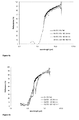
- Figure 4a shows the reflectance response from samples of G2 SS SiO 2 that were treated for 30, 60 and 120 minutes and the reflectance response from the untreated reference sample G2 SS SiO 2 Ref.
- Figure 4b shows the reflectance response from samples of G2 SS, hence samples without SiO 2 layer, that were treated for 30, 60 and 120 minutes and the reflectance response from the untreated reference sample G2 SS Ref.
- Figure 4c shows the reflectance response from samples of G2 Cu SiO 2 that were treated for 30, 60 and 120 minutes and the reflectance response from the untreated reference sample G2 Cu SiO 2 Ref.
- Figure 4d shows the reflectance response from samples of G2 Cu (without SiO 2 ) that were treated for 30, 60 and 120 minutes and the reflectance response from the untreated reference sample G2 SS Ref.
- Figure 5a is a bar diagram which shows the absorptance ⁇ s for samples of G2 Cu SiO 2 that were condensation tested for 30, 60 and 120 minutes as well as reference sample G2 Cu SiO 2 ref.
- Figure 5a also shows the absorptance ⁇ s for condensation tested samples of G2 SS SiO 2 and reference sample G2 SS SiO 2 ref.
- Figure 5a further shows the absorptance of materials G2 Cu and G2 SS. These materials will be discussed under figure 5c . It is apparent from figure 5a that for both types of substrates (SS) and (Cu) there is no significant difference in absorptance between the condensation tested samples and the untreated reference samples of the inventive material. This is true for all three testing periods, 30, 60 and 120 minutes.
- Figure 5b is a bar diagram which shows the emittance ⁇ t for samples of G2 Cu SiO 2 that were condensation tested for 30, 60 and 120 minutes as well as the emittance for reference sample G2 Cu SiO 2 ref.
- Figure 5b also shows the emittance ⁇ t for samples of G2 SS SiO 2 that were condensation tested for 30, 60 and 120 minutes as well as the emittance for reference sample G2 SS SiO 2 ref.
- Figure 5b shows that for both types of substrates (SS) and (Cu) there is no significant difference in emittance between the condensation tested samples and the untreated reference samples of the inventive materials. Hence, both the materials G2 SS SiO 2 and G2 Cu SiO 2 show good humidity resistance.
Landscapes
- Engineering & Computer Science (AREA)
- Physics & Mathematics (AREA)
- Life Sciences & Earth Sciences (AREA)
- Sustainable Development (AREA)
- Sustainable Energy (AREA)
- Thermal Sciences (AREA)
- Chemical & Material Sciences (AREA)
- Combustion & Propulsion (AREA)
- Mechanical Engineering (AREA)
- General Engineering & Computer Science (AREA)
- Spectroscopy & Molecular Physics (AREA)
- Laminated Bodies (AREA)
Abstract
a multilayer structure (30) for absorbing solar light;
a metallic substrate (20) for conducting heat from said multilayer structure (30), wherein said multilayer structure 30), in order from said substrate (20), at least comprises:
a first layer (100) of Al2O3;
a second layer (200) of Mo;
a third layer (300) of Al2O3;
an uppermost layer (700) of SiO2
Description
- The present invention relates to a solar thermal absorber material according to the preamble of
claim 1. - Solar thermal absorbers are typically used in household applications for converting sunlight into heat. These absorbers are usually referred to as "low temperature flat plate absorbers" as the typical operating temperature is below 400°C. A solar thermal absorber typically comprises a plate-like substrate of heat conductive metal such as copper, steel or aluminium. Fluid conducting tubes are attached to one side of the metallic plate, the inner side thereof, whereas the outer side of the plate is coated with a thin dark surface coating. The properties of the dark coating are such that the coating reflects very little of incident sunlight. Therefore, when the dark surface coating is exposed to sunlight it absorbs heat from the sunlight and thereby heats the metallic plate. The heat is transferred from the metallic plate to a fluid, for example water, which circulates in the tubes on the rear side of the plate. The heated fluid can be used in various household heating applications, such as heating of tap water. Typically, solar thermal absorbers of this type are enclosed in box-like protective housings comprising a transparent window and are arranged on the roofs of buildings.
- In a known material for solar thermal absorbers the dark coating is a multilayer structure having layers of Al2O3, SiO2, Mo, SiO2, Mo, SiO2 in order from the substrate. The multilayer structure is applied onto a metallic strip substrate of copper, stainless steel or aluminium.
- Although proven effective, this known type of solar thermal absorber material has occasionally exhibited low resistance against high temperatures and moisture induced corrosion. For example, moisture induced corrosion has occurred on solar absorbers based on copper substrate having the above mentioned multilayer structure. Solar absorbers of the above type that are based on aluminium substrates have somewhat better corrosion resistance than the ones comprising a copper substrate but does not have satisfactory heat resistance. Therefore, when the above types of solar absorbers are exposed for long periods to warm and humid weather conditions the properties of the absorbers tend to deteriorate, which shortens the service life of the absorbers.
- It is therefore an object of the present invention to provide a solar thermal absorber material which is resistant to heat and corrosion.
- This object is achieved by a solar thermal absorber material comprising:
- a multilayer structure for absorbing solar light;
- a metallic substrate for conducting heat from said multilayer structure, characterized in that said multilayer structure, in order from said substrate, at least comprises:
- a first layer of Al2O3;
- a second layer of Mo;
- a third layer of Al2O3;
- a fourth, uppermost, layer of SiO2,
- The inventive solar thermal absorber material has very high resistance to moisture induced corrosion and high temperatures.
- The "heat resistance" of a solar absorber material is in general the ability of the material to withstand high temperatures without losing its heat retaining capacity or having the layer structure crack or delaminating from the substrate.
- In the inventive solar thermal absorber material, the resistance to heat, and also to some extent the resistance to moisture-induced corrosion, is believed to be influenced by the fact that the alternating layers of aluminium oxide (Al2O3) and molybdenum (Mo) molybdenum have similar thermal expansion coefficients.
- When the inventive absorber material is heated, the layers of Al2O3 and Mo expand uniformly and substantially no strain or tension forms in the layer structure which otherwise would have caused the layer structure to break and to delaminate from the substrate.
- Corrosion in solar absorbers is generally caused by moisture from the atmosphere around the solar absorber that penetrates through the multilayer structure down to the metallic substrate and form oxides/hydroxides thereon. The oxides/hydroxides deteriorate the adhesion between the multilayer structure and the substrate which causes the multilayer structure to delaminate from the substrate.
- The high resistance to corrosion in the inventive material is believed to be caused by the following factors:
- As described above, the alternating layers of Al2O3 and Mo in the inventive material have similar thermal expansion coefficients. When these layers are heated they expand uniformly and therefore strain and tension is avoided in the layer structure which otherwise could have caused cracks through which moisture can penetrate down to the substrate.
- The outermost layer of the inventive multilayer structure is a layer of SiO2. It is believed that the layer of SiO2 absorbs moisture and therefore prevents moisture from penetrating through the underlying layers of Al2O3 and Mo to the surface of the metallic substrate. Even though the thermal expansion coefficient of SiO2 is different from the thermal expansion coefficient of Mo and Al2O3 tensions does not build up in the multilayer structure when the structure is heated since the SiO2 layer is the outermost layer.
- In the inventive multilayer structure it is important that the outermost SiO2 layer is applied directly onto an underlying Al2O3 layer. The reason therefore is that SiO2 and Al2O3 have similar refraction index. Therefore the optical properties of the multilayer structure, i.e. the ratio of absorptance/emittance are not negatively influenced to a significant extent by the SiO2 layer. This could otherwise have been the case if the SiO2 layer was applied onto another layer than Al2O3, for instance Mo.
- According to one embodiment, the multilayer structure defined above comprises:
- a first layer (100) of Al2O3 having a thickness of 28 - 89 nm;
- a second layer (200) of Mo having a thickness of 16 - 30 nm;
- a third layer (300) of Al2O3 having a thickness of 39 - 74 nm;
- an uppermost layer (700) of SiO2 having a thickness of 39 - 74 nm;
- According to a first preferred embodiment, the multilayer structure has the following configuration, preferably with layer thicknesses as indicated:
- a first layer of Al2O3 having a thickness of 10 - 240 nm;
- a second layer of Mo having a thickness of 8 - 120 nm;
- a third layer of Al2O3 having a thickness of 25 - 105 nm;
- a forth layer of Mo having a thickness of 3-60 nm;
- a fifth layer of Al2O3 having a thickness of 15-100 nm;
- a sixth, uppermost, layer of SiO2 having a thickness of 10 - 160 nm, wherein
- The described inventive multilayer structure comprises a large number of layers, in total five alternating layers of Al2O3 and Mo and the sixth layer of SiO2. The high number of layers has a positive effect on the corrosion resistance for the following reason:
- In a multilayer structure, defects, such as grain boundaries or micro cracks, in each individual layer may line up and form a passage for moisture through the layer structure. However, the probability that the defects in the individual layers line up to form a passage decreases with the number of individual layers in the structure. In other words, a defect in one layer is sealed by an adjacent layer.
- In order to achieve an even higher number of layers in the inventive multilayer structure without compromising the optical properties of the absorber, the middlemost Al2O3 layer could be formed by two individual Al2O3 layers, which are applied next to each other. The effect thereof is that a large number of layers are achieved in the multilayer structure which provides for good protection against moisture penetration. However, from an optical perspective the two adjacent Al2O3 layers only constitute one Al2O3 layer and do therefore not alter the optical properties of the solar thermal material.
- It is therefore preferred that the multilayer structure has the following configuration, preferably with layer thicknesses as indicated:
- a first layer of Al2O3 having a thickness of 10 - 240 nm;
- a second layer of Mo having a thickness of 8 - 120 nm;
- a third layer of Al2O3;
- a fourth layer of Al2O3;
- wherein the total thickness of said third and fourth layer is 25 - 105 nm;
- a fifth layer of Mo having a thickness of 3-60 nm;
- a sixth layer of Al2O3 having a thickness of 15-100 nm;
- a seventh, uppermost, layer of SiO2 having a thickness of 10 - 160 nm,
- In order to further minimize, or even eliminate, the effect that the SiO2 layer has on the optical properties of the multilayer structure it is preferred to adapt the thicknesses of the SiO2 layer and the underlying Al2O3 layer to each other. As mentioned above, the refraction indexes of Al2O3 and SiO2 are similar. However, for all wavelengths the refraction index of Al2O3 is slightly higher than that of SiO2. To compensate for this difference the SiO2 layer should preferably be thicker than the Al2O3 layer. Since the specific refraction indexes of Al2O3 and SiO2 varies with the wavelength, the precise relationship between thicknesses of the layers has to be determined by the skilled person. For example if the SiO2 layer has a thickness of 50 nm, the underlying Al2O3 layer should have a thickness of 45 nm for maintaining the desired optical properties of the solar thermal absorber material.
- In order to achieve very good corrosion resistance, thick layers could be provided in the multilayer structure. The maximum thickness of the layers should however be limited in order to prevent that thermal expansion cause tension and strain in the multilayer structure. The optical properties, i.e absorptance and emittance, will also deteriorate if the total thickness of the layer structure become too large. If the total thickness of the multilayer structure exceeds 300 nm less light will be reflected from the substrate back into the multilayer structure and therefore the emittance will increase and the absorptance decrease.
- The layers or some of the layers in the inventive multilayer structure could be made very thin. The advantage thereof is that a good compromise between absorptance and emittance is obtained. However, it is difficult to achieve very thin coherent layers and the minimum thickness of the layers should therefore be limited in order to secure that all layers of the inventive multilayer structure are intact and fully closed coalesced thin films.
- According to a third preferred embodiment, the layers in the inventive multilayer structure may have the following thicknesses:
- the first layer of Al2O3, a thickness of 45-100 nm;
- the second layer of Mo, a thickness of 15 - 33 nm;
- the third layer and the fourth layer (400) of Al2O3, a total thickness 38 - 83 nm;
- the fifth layer of Mo, a thickness of 8 - 16 nm;
- the sixth layer of Al2O3, a thickness of 34 - 75 nm;
- the seventh layer of SiO2, a thickness of 38 - 83 nm.
- A solar thermal absorber material comprising this multilayer structure has a robust coherent multilayer structure which provides for good corrosion resistance and good thermal stability.
- The thickness of the Mo layers in the multilayer structure may be selected such that the first Mo layer is twice as thick as the second Mo layer. Thereby a gradient having a low metal fraction towards the surface is obtained in the layer structure. It is preferred to have a metal gradient through the layer structure for the following reason: The solar absorber material shall absorb as much solar light as possible and it is therefore preferred that it in total contains a high fraction of metal. However, close to the surface of the solar absorber the fraction of metal shall be low in order to not influence the refraction index of the layer structure.
- Preferably the thicknesses of the layers according to this alternative are selected such that:
- the first layer of Al2O3 having a thickness of 60 nm;
- the second layer of Mo having a thickness of 12 - 42 nm;
- the third layer and the fourth layer of Al2O3 having a total thickness of 50 nm;
- the fifth layer of Mo having a thickness of 6 - 21 nm;
- the sixth layer of Al2O3 having a thickness of 45 nm;
- the seventh layer of SiO2 having a thickness of 50 nm;
- According to a fourth preferred embodiment the solar thermal absorber material comprises a multilayer structure having the following layer thicknesses:
- the first layer of A2O3 has a thickness of 60 nm;
- the second layer of Mo has a thickness of 20 nm;
- the third layer and the fourth layer of Al2O3 has a total thickness of 50 nm;
- the fifth layer of Mo has a thickness of 10 nm;
- the sixth layer of Al2O3 has a thickness of 75 nm;
- the seventh layer of SiO2 has a thickness of 50 nm.
- Preferably the sixth layer of Al2O3 has a thickness of 45 nm.
- The metallic substrate of the inventive solar thermal absorber is preferably selected from copper strip, aluminium strip or stainless steel strip. Such materials have good thermal conductivity and are therefore suitable for use in solar thermal absorbers. Copper and aluminium strip further exhibits adequate reflectance property which is essential for providing low emittance properties in the inventive solar absorber material.
-
-
Figure 1 : A schematic drawing of a cross section through the inventive solar thermal absorber material according to a preferred embodiment. -
Figure 2a and2b shows the reflectance responses of heat treated samples of G2 SS SiO2, G2 Cu SiO2 and an untreated reference sample G2 SS SiO2 ref, G2 SS SiO2 ref. -
Figure 3a and 3b show absorptance α s and emittance ε t upon heat treatment for samples G2 SS SiO2, G2 Cu SiO2 and reference samples G2 SS SiO2 ref, G2 SS SiO2 ref and samples of G2 Cu/SS. -
Figure 3c shows the performance criterion for heat treated samples offigures 3a and 3b . -
Figure 4a show the reflectance response from samples of G2 SS SiO2 and an untreated reference sample G2 SS SiO2 ref that were subjected to condensation treatment. -
Figure 4b show the reflectance response after condensation treatment from samples of G2 SS that have the same multilayer structure as the samples infigure 4a but without a SiO2 layer.Figure 4b also shows the reflectance response from an untreated reference sample G2 SS ref. -
Figure 4c show the reflectance response from samples of G2 Cu SiO2 and an untreated reference sample G2 Cu SiO2 ref that were subjected to condensation treatment. -
Figure 4d show the reflectance response after condensation treatment from samples of G2 Cu that have the same multilayer structure as the samples infigure 4c but without a SiO2 layer.Figure 4d also shows the reflectance response from an untreated reference sample G2 Cu ref. -
Figure 5a and 5b show absorptance α s and emittance ε t upon condensation testing for samples G2 SS SiO2, G2 Cu SiO2 and reference samples G2 SS SiO2 ref, G2 SS SiO2 ref and samples G2 Cu/SS. -
Figure 5c shows the performance criterion for the samples offigure 5a and 5b subjected to condensation test. -
Figure 1 shows the inventive solar thermal absorber material according to a preferred embodiment. The solarthermal absorber material 10 comprises asubstrate 20 which is made of strip of metallic material, preferably copper, aluminium or stainless steel, for example of the sort 15R10. Thesubstrate 20 may have a thickness of 0,1-0,4 mm. and its length and width are adapted for the actual application. - A
multilayer structure 30 is applied onto the substrate. The multilayer structure has the following configuration: closest to the substrate is alayer 100 of aluminium oxide (Al2O3) thereafter asecond layer 200 of Molybdenum (Mo) onto which a third and afourth layer fifth layer 500 of Mo, asixth layer 600 of Al2O3 and a seventh 700, outermost layer of SiO2. - The inventive solar thermal absorber material is manufactured by coating a strip material with layers of Al2O3, Mo and SiO2 using physical vapour deposition (PVD) in a continuous roll-to-roll process. Preferably, the surface of the strip material is ion-etched prior to coating in order to provide good adhesion between the multilayer structure and the surface of the strip material.
- Preferably the thicknesses of the individual layers in the inventive solar absorber material should be:
layer 100 of Al2O3: 10-240 nm;layer 200 of Mo: 8-120 nm;layer 300 of Al2O3: 25-50 nm;layer 400 of Al2O3: 25-50;layer 500 of Mo: 3-60;layer 600 of Al2O3: 15-45 nm;layer 700 of SiO2: 10-50 nm. - The thicknesses of each individual layer should be selected to be within the stated intervals such that the ratio of absorptance/emittance of the solar thermal absorber material is ≥90%/≤10% for the selected substrate.
- The ratio between the absorptance/emittance of the solar absorber is a measure on the thermal efficiency of the solar absorber. It is desired to have as high absorptance as possible since as much sunlight as possible shall be absorbed and transferred as heat to the substrate. However in operation, the solar absorber heats up and start to radiate heat. The radiated heat is measured as emittance and can be considered a heat loss from the solar absorber. It is generally accepted that an efficient commercial solar absorber should have an absorptance/emittance ratio of ≥90%/≤10% at its operation temperature. However, an thermal solar absorber having an absorptance/emittance ratio of ≥80%/≤20% is also fully functional.
- It is believed that the ratio of absorptance/emittance is influenced by the material in the individual layers and the infra-red properties of the substrate. For example a high fraction of metal in the layer structure has a positive effect on the absorptance. Although no explanation can be given it is further believed that the thicknesses of the individual layers also are of importance for the absorptance/emittance ratio of the solar absorber material.
- The individual layer thicknesses of the inventive solar absorber material according to the above described embodiment were determined from simulations performed using the computer program TS-Calc Thinfilm by Software Specta Inc. In the simulation an initial layer structure was entered in the program. The initial layer structure had the thicknesses:
-
Layer 1 Al2O3: 60 nm; Layer 2 Mo: 20 nm, layer 3 and 4 Al2O3: 50 nm in total; Layer 5 Mo: 10 nm; Llayer 6 Al2O3: 45 nm; Layer 7 SiO2: 50 nm. - Thereafter the thickness of each individual layer was varied to determine the maximum and minimum thickness of each layer under the condition that an absorptance/emittance ratio of ≥90%/≤10% was maintained. Table 1 shows the results of the simulation.
Table 1: Results from simulation in TS-Calc on seven layer structure Layer 1 Layer 2 Layer 3/4 Layer 5 Layer 6 Layer 7 Al2O3 Mo Al2O3/ Al2O3 Mo Al2O3 SiO2 Absorptance/ Emittance 240 20 50 10 45 50 ≥90%/≤10% 10 20 50 10 45 50 ≥90%/≤10% 60 120 50 10 45 50 ≥90%/≤10% 60 8 50 10 45 50 ≥90%/≤10% 60 20 105 10 45 50 ≥90%/≤10% 60 20 25 10 45 50 ≥90%/≤10% 60 20 50 20 45 50 ≥90%/≤10% 60 20 50 3 45 50 ≥90%/≤10% 60 20 50 10 100 50 ≥90%/≤10% 60 20 50 10 15 50 ≥90%/≤10% 60 20 50 10 45 160 ≥90%/≤10% 60 20 50 10 45 10 ≥90%/≤10% - In the described embodiment above, the layer structure has six layers of Al2O3 and
- Mo and a seventh layer of SiO2. However, simulations in TS-Calc have shown that a functional solar thermal absorber having an absorptance/emittance ratio of ≥80%/≤20% may be achived with a multilayer structure having
first layer 100 of Al2O3, asecond layer 200 of Mo, athird layer 300 of Al2O3 and an uppermost, layer of SiO2. The simulations were performed as described above with a starting structure of: -
Layer 1 Al2O3: 60 nm; Layer 2 Mo: 20 nm, Layer 3 of Al2O3: 50 nm and the outermost SiO2 layer 50 nm. - The layers were varied under the condition that the absorptance/emittance ratio should be ≥80%/≤20%.Table 2 shows the results of the simulation.
Table 2: Results from simulation in TS-Calc on three layer structure. Layer 1Layer 2 Layer 3 Layer 4 Absorptance/Emittance Al2O3 Mo Al2O3 SiO2 ≥80%/≤20% 28 16 39 39 ≥80%/≤20% 36 16 41 41 ≥80%/≤20% 44 17 42 43 ≥80%/≤20% 51 18 45 45 ≥80%/≤20% 57 19 48 48 ≥80%/≤20% 63 21 53 53 ≥80%/≤20% 66 22 55 55 ≥80%/≤20% 69 23 58 58 ≥80%/≤20% 73 24 61 61 ≥80%/≤20% 77 26 64 64 ≥80%/≤20% 80 27 67 67 ≥80%/≤20% 84 28 70 70 ≥80%/≤20% 89 30 74 74 ≥80%/≤20% - Above specific layer thicknesses that yield solar thermal absorbers having acceptable absorptance/emittance ratios have been disclosed. However it is obvious that the skilled person, within the defined ranges, can determine other layer thicknesses that are suitable for a certain type of application of the solar thermal absorber The skilled person may determine these values by simulations as described above or by practical experiments as described below.
- The inventive solar thermal absorber material will in the following be described in detail in with reference to tests that have been performed on samples of the inventive solar thermal material.
- Samples of the inventive solar thermal absorber material were produced by coating strip substrates of stainless steel (SS) of the type 15R10 and copper (Cu) with the inventive multilayer structure in a continuous roll-to-roll PVD coating line. These samples were denominated G2 SS Si02 and G2 Cu Si02. The targeted thicknesses for the individual layers of the multilayer structure were as follows (from the substrate): Al2O3 (60 nm), Mo (20 nm), Al2O3 (25 nm), Al2O3 (25 nm), Mo (10 nm), Al2O3 (75 nm) and finally SiO2 (50 nm).
- For determining the effect of the SiO2 layer, two sets of samples G2 Cu and G2 SS with were produced. These samples have the above layer structure but without SiO2 layer. The thicknesses of the layers were determined in SEM (Scanning Electron Microscope). Table 2 shows the total set of samples that were produced.
Table 3: Test samples Sample Id Thickness (nm) Al2O3 /Mo/Al2O3 / Al2O3 /Mo/Al2O3 /SiO2 G2 SS Si02 60/20/25/25/10/75/50 G2 Cu Si02 60/20/25/25/10/75/50 G2 SS 60/20/25/25/10/75 G2 Cu 60/20/25/25/10/75 - Some samples of each material were put aside as reference material. These materials are in the following referred to as G2 SS SiO2 ref, G2 Cu SiO2 ref and G2 SS ref, G2 Cu ref. These samples were not subjected to any treatment
- Other samples of each material were subjected to a heat test and a condensation test respectively. The heat test and the condensation test simulate accelerated climate influence on the chemical behaviour and optical properties of the samples. Therefore these tests are good measures on the ability of the material to resist heat and corrosion for prolonged periods of time.
- The heat test is a measure on the ability of the inventive solar thermal absorber material to resist high temperatures. In the heat test, samples of each type (G2 SS SiO2, G2 Cu SiO2 and G2 SS, G2 Cu) were placed in a closed oven (containing non-circulating hot air) at 240°C (Cu) and 300°C (SS). The reduced temperature for Cu was chosen from experience indicating a generally lower resistance towards heat compared to SS. All samples were treated for a duration of 192 hours.
- The condensation test is a measure of the corrosion resistance of the inventive solar thermal absorber material. In the condensation test, samples of each type (G2 SS SiO2, G2 Cu SiO2 and G2 SS, G2 Cu) were held ∼5 cm above the water surface in a pot of boiling water (municipal, not deionized) held at 95°C. Water vapour was condensed onto the samples at a sample temperature of about 45°C. Times of treatment were 30 min, 60 min and 120 min.
- After heat treatment and condensation testing, the long term stability of the optical performance on α s (absorptance) and ε t (emittance) of the samples was determined. The optical performance is a measure on how much the absorptance α s and emittance ε t of the treated samples has changed in comparison to untreated reference samples.
- The samples, treated and untreated, were investigated with a Carl Zeiss CORONA Plus VIS-NIR dual-beam spectrometer in the wavelength interval 0.38 to 2.15 µm and a Bruker 27 FTIR spectrometer for wavelengths in the span 2.5 - 24 µm. The obtained data is defined as reflectance R(λ) and furthermore used in the evaluation equations of solar absorptance (1) and thermal emittance (2) below.
- The normal solar absorptance, α s , is weighted with the solar spectral radiation, Is (λ), and is defined by

- The solar spectral radiation, IS (λ), is defined in the wavelength range from 0.3 - 4.1 µm. The data obtained from the Carl Zeiss spectrometer is therefore extrapolated for wavelengths between 0.30 and 0.38 µm.
- The total normal thermal emittance, ε t , is weighted with the blackbody spectrum, IBb (λ,T), for a given temperature T (Normally T is chosen to be 373 K). The emittance is defined by

- For classifying the long term stability of the optical performance on α s and ε t the performance criterion (PC) as defined by the international energy agency (IEA) was applied:

where the change in solar absorptance Δα s is defined as
with α s,t corresponding to the value of solar absorptance of the treated samples and with α s,i corresponding to the solar absorptance of the untreated reference samples. - The change in thermal emittance Δε t is defined as

with ε t,t corresponding to the value of thermal emittance of the treated samples at the actual time of the test and with ε t,i corresponding to the thermal emittance of the untreated reference samples. - According to IEA, a value of PC should generally not exceed 0.05 after climate treatment.
- The absorptance α s , the emittance ε t and the performance criterion (PC) was determined for the samples using the equations (1) - (5). These results and the reflectance measurements are presented below for the heat treated and the condensation tested samples respectively.
-
Figure 2a shows the reflectance responses of the heat treated sample of G2 SS SiO2 and the untreated reference sample G2 SS SiO2 ref. -
Figure 2b shows the reflectance responses of the heat treated sample of G2 Cu SiO2 and the untreated reference sample G2 Cu SiO2 ref. - No significant change of in the reflectance response between the untreated sample (Ref) and the treated samples can be seen in
figures 3a and 3b . Consequently, no significant deterioration of the heat treated samples has occurred. -
Figure 3a is a bar diagram which shows the absorptance α s for heat treated sample G2 Cu SiO2 and for reference sample G2 Cu SiO2 ref.Figure 3a also shows the absorptance α s for heat treated sample G2 SS SiO2 and reference sample G2 SS SiO2 ref.Figure 3a also shows the results for G2 Cu and G2 SS. These materials will be discussed underfigure 3c . Regarding the inventive material, G2 Cu SiO2 and G2 SS SiO2, it is apparent fromfigure 3a that for both types of substrates (SS) and (Cu) there is no significant difference in absorptance between the heat treated samples and the untreated reference samples. -
Figure 3b is a bar diagram which shows the emittance ε t for heat treated sample G2 Cu SiO2 and reference sample G2 Cu SiO2 ref.Figure 3b also shows the emittance ε t for heat treated sample G2 SS SiO2 and reference sample G2 SS SiO2 ref. Materials G2 Cu and G2 SS will be discussed underfigure 3c . It is apparent fromfigure 3b that for both types of substrates (SS) and (Cu) there is no significant difference in emittance between the heat treated samples and the untreated reference samples of the inventive material. - The changes in optical performance for the heat treated samples are presented by the performance criterion PC in
Figure 3c . It is clear fromfigure 3c that both samples of the inventive material are below the criterion limit of 0,05. Sample G2 Cu SiO2 has a performance criterion value of 0,005 and sample G2 SS SiO2 has a performance criterion value of 0,016. Hence, no significant deterioration of the optical performance has occurred in the heat treated samples and they are consequently exhibiting good heat resistance. - When the performance criterion of the samples G2 SS SiO2 and G2 Cu SiO2 is compared with the samples G2 Cu and G2 SS (without Si02 layer) it is further clear that the performance criterion upon heat treatment for copper substrates is improved by the Si02 layer.
-
Figure 4a shows the reflectance response from samples of G2 SS SiO2 that were treated for 30, 60 and 120 minutes and the reflectance response from the untreated reference sample G2 SS SiO2 Ref. -
Figure 4b shows the reflectance response from samples of G2 SS, hence samples without SiO2 layer, that were treated for 30, 60 and 120 minutes and the reflectance response from the untreated reference sample G2 SS Ref. -
Figure 4c shows the reflectance response from samples of G2 Cu SiO2 that were treated for 30, 60 and 120 minutes and the reflectance response from the untreated reference sample G2 Cu SiO2 Ref. -
Figure 4d shows the reflectance response from samples of G2 Cu (without SiO2) that were treated for 30, 60 and 120 minutes and the reflectance response from the untreated reference sample G2 SS Ref. - In
figure 4b andfigure 4d , which shows the samples without a SiO2 layer, a typical hygroscopic response is shown around 3 nm for both substrates. This can be seen by the sharp dip in the reflectance response around 3 nm. For the Cu substrate, seefigure 4d , the response became worse for wavelengths up to 2 nm, this is seen in the higher overall reflectance indicating a change in the multilayer structure. After 120 min of condensation treatment the absorber surface properties are deteriorated in the entire spectrum. In comparison withfigures 4a and4c , which shows the results from samples having a multilayer structure including the Si02 layer, it is clear that the reflectance response remain unaffected upon the different lengths of condensation treatment. The typical hygroscopic behaviour seen infigures 4b and4d is not visible at all. Hence the Si02 layer increases the resistance to humidity in the multilayer structure. It should also be noted that when the condensation treated samples of G2 Cu SiO2 and G2 SS SiO2 are compared with the untreated reference samples G2 Cu SiO2 ref and G2 SS SiO2 ref, no significant difference can be noted between condensation tested samples and the reference samples. -
Figure 5a is a bar diagram which shows the absorptance α s for samples of G2 Cu SiO2 that were condensation tested for 30, 60 and 120 minutes as well as reference sample G2 Cu SiO2 ref.Figure 5a also shows the absorptance α s for condensation tested samples of G2 SS SiO2 and reference sample G2 SS SiO2 ref.Figure 5a further shows the absorptance of materials G2 Cu and G2 SS. These materials will be discussed underfigure 5c . It is apparent fromfigure 5a that for both types of substrates (SS) and (Cu) there is no significant difference in absorptance between the condensation tested samples and the untreated reference samples of the inventive material. This is true for all three testing periods, 30, 60 and 120 minutes. -
Figure 5b is a bar diagram which shows the emittance ε t for samples of G2 Cu SiO2 that were condensation tested for 30, 60 and 120 minutes as well as the emittance for reference sample G2 Cu SiO2 ref.Figure 5b also shows the emittance ε t for samples of G2 SS SiO2 that were condensation tested for 30, 60 and 120 minutes as well as the emittance for reference sample G2 SS SiO2 ref.Figure 5b shows that for both types of substrates (SS) and (Cu) there is no significant difference in emittance between the condensation tested samples and the untreated reference samples of the inventive materials. Hence, both the materials G2 SS SiO2 and G2 Cu SiO2 show good humidity resistance. - The changes in optical performance are presented by the performance criterion PC, see
Figure 5c . As seen infigure 5c both materials G2 SS SiO2 and G2 Cu SiO2 resist the treatment well and are all clearly below the criterion limit of 0,05. When the performance criterion of samples of G2 Cu and G2 SS are compared with the samples of G2 Cu SiO2 and G2 Cu SiO2 it is clear that the performance criterion for both types of substrates benefits from the additional Si02 layer. - To summarize, the above results show that the optical performance of the heat treated and the condensation tested samples remain well below the IEA performance criterion of 0,05. This proves that the inventive solar thermal absorber material has high resistance to both heat and moisture induced corrosion.
Claims (15)
- A solar thermal absorber material (10) comprising:a multilayer structure (30) for absorbing solar light;a metallic substrate (20) for conducting heat from said multilayer structure (30), characterized in that said multilayer structure 30), in order from said substrate (20), at least comprises:a first layer (100) of Al2O3;a second layer (200) of Mo;a third layer (300) of Al2O3;an uppermost layer (700) of SiO2.
- The solar thermal absorber material (10) according to claim 1, wherein said multilayer structure 30), in order from said substrate (20), comprises:a first layer (100) of Al2O3 having a thickness of 28 - 89 nm;a second layer (200) of Mo having a thickness of 16 - 30 nm;a third layer (300) of Al2O3 having a thickness of 39 - 74 nm;an uppermost layer (700) of SiO2 having a thickness of 39 - 74 nm;wherein the thickness of the layers is selected such that the ratio of absorptance/emittance is ≥80/≤20.
- The solar thermal absorber material (10) according to claim 1, wherein said multilayer structure (30), in order from said substrate (20), at least comprises:a first layer (100) of Al2O3;a second layer (200) of Mo;a third layer (300) of Al2O3;a fourth layer (500) of Mo;a fifth layer (600) of Al2O3;an uppermost layer (700) of SiO2.
- The solar thermal absorber material (10) according to claim 3, wherein said multilayer structure (30), in order from said substrate (20), comprises:a first layer (100) of Al2O3 having a thickness of 10 - 240 nm;a second layer (200) of Mo having a thickness of 8 - 120 nm;a third layer (300) of Al2O3 having a thickness of 25 - 105 nm;a fourth layer (500) of Mo having a thickness of 3-60 nm;a fifth layer (600) of Al2O3 having a thickness of 15-100 nm;an uppermost layer (700) of SiO2 having a thickness of 10 - 160 nm, whereinthe thickness of the layers is selected such that the ratio of absorptance/emittance is ≥90/≤10.
- The solar thermal absorber material (10) according to claim 3, wherein said multilayer structure (30), in order from said substrate (20), comprises:a first layer (100) of Al2O3;a second layer (200) of Mo;a third layer (300) of Al2O3;a fourth layer (400) of Al2O3,a fifth layer (500) of Mo;a sixth layer (600) of Al2O3;an uppermost layer (700) of SiO2
- The solar thermal absorber material (10) according to claim 5, wherein said multilayer structure 30), in order from said substrate (20), comprises:a first layer (100) of Al2O3 having a thickness of 10 - 240 nm;a second layer (200) of Mo having a thickness of 8 - 120 nm;a third layer (300) of Al2O3;a fourth layer (400) of Al2O3,wherein the total thickness of said third and fourth layer is 25 - 105 nm;a fifth layer (500) of Mo having a thickness of 3-60 nm;a sixth layer (600) of Al2O3 having a thickness of 15-100 nm;an uppermost layer (700) of SiO2 having a thickness of 10 - 160 nm, whereinthe thickness of the layers is selected such that the ratio of absorptance/emittance is ≥90/≤10.
- The solar thermal absorber material (10) according to claim 6, wherein:the first layer (100) has a thickness of 45 - 100 nm;the second layer (200) has a thickness of 15 - 33 nm;the third layer (300) and the fourth layer (400) has a total thickness 38 - 83 nm;the fifth layer (500) has a thickness of 8 - 16 nm;the sixth layer (600) has a thickness of 34 - 75 nm;the uppermost layer (700) of SiO2 has a thickness of 38 - 83 nm.
- The solar thermal absorber material (10) according to claim 7, wherein:the first layer (100) has a thickness of 60 nm;the second layer (200) has a thickness of 20 nm;the third layer (300) and the fourth layer (400) has a total thickness of 50 nm;the fifth layer (500) has a thickness of 10 nm;the sixth layer (600) has a thickness of 75 nm;the uppermost layer (700) of SiO2 has a thickness of 50 nm.
- The solar thermal absorber material (10) according to any of the preceding claims, wherein the thickness of the uppermost layer (700) of SiO2 is greater than the thickness of the underlying layer (300), (600) of Al2O3.
- The solar thermal absorber material (10) according to claim 8, wherein:the sixth layer (600) has a thickness of 45 nm.
- The solar thermal absorber material (10) according to any of claims 3-11, wherein the thickness of the molybdenum layers (200), (500) are selected such that gradient of Mo concentration is achieved in the multilayer structure, wherein said gradient decreases towards the uppermost layer (700) of SiO2.
- The solar thermal absorber material according to claim 12, wherein the thickness of the molybdenum layer closest to the substrate (200) is approximately twice as thick as the uppermost molybdenum layer (500).
- The solar thermal absorber material (10) according to claim 13, wherein:the first layer (100) has a thickness of 60 nm;the second layer (200) has a thickness of 12 - 42 nm;the third layer (300) and the fourth layer (400) has a total thickness of 50 nm;the fifth layer (500) has a thickness of 6 - 21 nm;the sixth layer (600) has a thickness of 45 nm;the uppermost layer (700) of SiO2 has a thickness of 50 nm;
- The solar thermal absorber material (10) according to any of the preceding claims, wherein the total thickness of the multilayer structure is less than 300 nm.
- The solar thermal absorber material (10) according to any of the preceding claims, wherein the substrate is a strip material selected from the group of stainless steel, copper and aluminium.
Priority Applications (3)
| Application Number | Priority Date | Filing Date | Title |
|---|---|---|---|
| EP11166762.2A EP2525162B1 (en) | 2011-05-19 | 2011-05-19 | A solar thermal absorber material |
| CN201280024367.6A CN103547871B (en) | 2011-05-19 | 2012-05-16 | Solar heat absorber material |
| PCT/EP2012/059150 WO2012156457A1 (en) | 2011-05-19 | 2012-05-16 | A solar thermal absorber material |
Applications Claiming Priority (1)
| Application Number | Priority Date | Filing Date | Title |
|---|---|---|---|
| EP11166762.2A EP2525162B1 (en) | 2011-05-19 | 2011-05-19 | A solar thermal absorber material |
Publications (2)
| Publication Number | Publication Date |
|---|---|
| EP2525162A1 true EP2525162A1 (en) | 2012-11-21 |
| EP2525162B1 EP2525162B1 (en) | 2013-07-17 |
Family
ID=46177406
Family Applications (1)
| Application Number | Title | Priority Date | Filing Date |
|---|---|---|---|
| EP11166762.2A Not-in-force EP2525162B1 (en) | 2011-05-19 | 2011-05-19 | A solar thermal absorber material |
Country Status (3)
| Country | Link |
|---|---|
| EP (1) | EP2525162B1 (en) |
| CN (1) | CN103547871B (en) |
| WO (1) | WO2012156457A1 (en) |
Citations (3)
| Publication number | Priority date | Publication date | Assignee | Title |
|---|---|---|---|---|
| DE2811393A1 (en) * | 1978-03-16 | 1979-09-27 | Reynolds Metals Co | Electroplating aluminium with thin solar energy absorbing coatings - comprising molybdenum and molybdenum oxide(s) |
| EP1217315A1 (en) * | 2000-12-20 | 2002-06-26 | ALANOD Aluminium-Veredlung GmbH & Co. KG | Solar collector element |
| EP2253737A1 (en) * | 2009-05-20 | 2010-11-24 | SCHOTT Solar AG | Radiation-selective absorber coating and absorber tube with radiation-selective absorber coating |
Family Cites Families (6)
| Publication number | Priority date | Publication date | Assignee | Title |
|---|---|---|---|---|
| US4442166A (en) * | 1979-11-15 | 1984-04-10 | Massachusetts Institute Of Technology | Cermet film selective-black absorber |
| JPS6259342A (en) * | 1985-09-06 | 1987-03-16 | Sumitomo Metal Ind Ltd | Solar heat collecting panel |
| DE4344258C1 (en) * | 1993-12-23 | 1995-08-31 | Miladin P Lazarov | Material from chemical compounds with a metal of group IV A of the periodic table, nitrogen and oxygen, its use and production method |
| CN101294749A (en) * | 2007-04-24 | 2008-10-29 | 梁美意 | Heat-collecting tube with solar energy selective absorption coating and manufacturing method thereof |
| CN201373612Y (en) * | 2009-02-17 | 2009-12-30 | 东莞市康达机电工程有限公司 | Solar High Temperature Selective Absorption Film |
| CN201407852Y (en) * | 2009-02-26 | 2010-02-17 | 东莞市康达机电工程有限公司 | High temperature selective absorption film for solar spectrum |
-
2011
- 2011-05-19 EP EP11166762.2A patent/EP2525162B1/en not_active Not-in-force
-
2012
- 2012-05-16 WO PCT/EP2012/059150 patent/WO2012156457A1/en not_active Ceased
- 2012-05-16 CN CN201280024367.6A patent/CN103547871B/en not_active Expired - Fee Related
Patent Citations (3)
| Publication number | Priority date | Publication date | Assignee | Title |
|---|---|---|---|---|
| DE2811393A1 (en) * | 1978-03-16 | 1979-09-27 | Reynolds Metals Co | Electroplating aluminium with thin solar energy absorbing coatings - comprising molybdenum and molybdenum oxide(s) |
| EP1217315A1 (en) * | 2000-12-20 | 2002-06-26 | ALANOD Aluminium-Veredlung GmbH & Co. KG | Solar collector element |
| EP2253737A1 (en) * | 2009-05-20 | 2010-11-24 | SCHOTT Solar AG | Radiation-selective absorber coating and absorber tube with radiation-selective absorber coating |
Non-Patent Citations (1)
| Title |
|---|
| ZHANG Q-C: "Recent progress in high-temperature solar selective coatings", SOLAR ENERGY MATERIALS AND SOLAR CELLS, ELSEVIER SCIENCE PUBLISHERS, AMSTERDAM, NL, vol. 62, no. 1-2, 1 April 2000 (2000-04-01), pages 63 - 74, XP004195297, ISSN: 0927-0248, DOI: 10.1016/S0927-0248(99)00136-1 * |
Also Published As
| Publication number | Publication date |
|---|---|
| CN103547871B (en) | 2016-08-17 |
| WO2012156457A1 (en) | 2012-11-22 |
| CN103547871A (en) | 2014-01-29 |
| EP2525162B1 (en) | 2013-07-17 |
Similar Documents
| Publication | Publication Date | Title |
|---|---|---|
| US6010602A (en) | Annealed low emissivity coating | |
| Hsieh et al. | Thermal radiative properties of glass from 0.32 to 206 μm | |
| ES2323155T3 (en) | STACKING OF LOW EMISSIVITY THIN LAYERS (LOW-E) WITH INTERMEDIATE LAYERS ANTIDIFUSION. | |
| CA2526067C (en) | Method of manufacturing an impact resistant and insulated glass unit composite with solar control and low-e coatings | |
| KR101499288B1 (en) | Low-emissivity coated board and building material including the same | |
| KR101873103B1 (en) | Functional building material including low-emissivity coat for windows | |
| RU2722384C2 (en) | Window glass containing functional coating | |
| RU2717490C2 (en) | Glass containing functional coating, including silver and indium | |
| DE102009022059A1 (en) | Radiation-selective absorber coating and absorber tube with radiation-selective absorber coating | |
| EA030242B1 (en) | Glass substrate with a coating, reflective member and method for producing said substrate | |
| Carlsson et al. | Comparison between predicted and actually observed in-service degradation of a nickel pigmented anodized aluminium absorber coating for solar DHW systems | |
| EP3511506A1 (en) | Low-emissivity coating, and functional building material for windows and doors comprising low-emission coating | |
| Miller et al. | Degradation in photovoltaic encapsulation strength of attachment: Results of the first PVQAT TG5 artificial weathering study | |
| EP2525162B1 (en) | A solar thermal absorber material | |
| Koehl | Durability of solar energy materials | |
| Kotilainen et al. | Temperature-induced ageing of solar absorbers on plain and anodized aluminium substrates | |
| Moncada et al. | Comparative experimental study of new absorbent surface coatings for flat plate solar collectors | |
| DiGrazia et al. | ReflecTech® mirror film attributes and durability for CSP applications | |
| Lazarov et al. | Optimization of SiO2-TiNxOy-Cu interference absorbers: numerical and experimental results | |
| IE43892B1 (en) | Coated transparent sheets | |
| Konttinen et al. | Microstructural optimization and extended durability studies of low-cost rough graphite–aluminium solar absorber surfaces | |
| CN103342022B (en) | The two silver low-radiation coated glass of a kind of fire prevention and manufacture method thereof | |
| US20120207922A1 (en) | Method of manufacturing eyeglass lens | |
| US20230348321A1 (en) | Transparent substrate provided with thin-film multilayer coating | |
| US12503392B2 (en) | Transparent substrate provided with thin multilayer coating |
Legal Events
| Date | Code | Title | Description |
|---|---|---|---|
| PUAI | Public reference made under article 153(3) epc to a published international application that has entered the european phase |
Free format text: ORIGINAL CODE: 0009012 |
|
| 17P | Request for examination filed |
Effective date: 20110519 |
|
| AK | Designated contracting states |
Kind code of ref document: A1 Designated state(s): AL AT BE BG CH CY CZ DE DK EE ES FI FR GB GR HR HU IE IS IT LI LT LU LV MC MK MT NL NO PL PT RO RS SE SI SK SM TR |
|
| AX | Request for extension of the european patent |
Extension state: BA ME |
|
| GRAP | Despatch of communication of intention to grant a patent |
Free format text: ORIGINAL CODE: EPIDOSNIGR1 |
|
| GRAS | Grant fee paid |
Free format text: ORIGINAL CODE: EPIDOSNIGR3 |
|
| GRAA | (expected) grant |
Free format text: ORIGINAL CODE: 0009210 |
|
| RBV | Designated contracting states (corrected) |
Designated state(s): AL AT BE BG CH CY CZ DE DK EE ES FI FR GB GR HR HU IE IS IT LI LT LU LV MC MK MT NL NO PL PT RO RS SE SI SK SM TR |
|
| AK | Designated contracting states |
Kind code of ref document: B1 Designated state(s): AL AT BE BG CH CY CZ DE DK EE ES FI FR GB GR HR HU IE IS IT LI LT LU LV MC MK MT NL NO PL PT RO RS SE SI SK SM TR |
|
| REG | Reference to a national code |
Ref country code: GB Ref legal event code: FG4D |
|
| REG | Reference to a national code |
Ref country code: CH Ref legal event code: EP |
|
| REG | Reference to a national code |
Ref country code: IE Ref legal event code: FG4D |
|
| REG | Reference to a national code |
Ref country code: AT Ref legal event code: REF Ref document number: 622459 Country of ref document: AT Kind code of ref document: T Effective date: 20130815 |
|
| REG | Reference to a national code |
Ref country code: DE Ref legal event code: R096 Ref document number: 602011002368 Country of ref document: DE Effective date: 20130912 |
|
| REG | Reference to a national code |
Ref country code: AT Ref legal event code: MK05 Ref document number: 622459 Country of ref document: AT Kind code of ref document: T Effective date: 20130717 |
|
| REG | Reference to a national code |
Ref country code: NL Ref legal event code: VDEP Effective date: 20130717 |
|
| REG | Reference to a national code |
Ref country code: LT Ref legal event code: MG4D |
|
| PG25 | Lapsed in a contracting state [announced via postgrant information from national office to epo] |
Ref country code: CY Free format text: LAPSE BECAUSE OF FAILURE TO SUBMIT A TRANSLATION OF THE DESCRIPTION OR TO PAY THE FEE WITHIN THE PRESCRIBED TIME-LIMIT Effective date: 20130918 Ref country code: SE Free format text: LAPSE BECAUSE OF FAILURE TO SUBMIT A TRANSLATION OF THE DESCRIPTION OR TO PAY THE FEE WITHIN THE PRESCRIBED TIME-LIMIT Effective date: 20130717 Ref country code: IS Free format text: LAPSE BECAUSE OF FAILURE TO SUBMIT A TRANSLATION OF THE DESCRIPTION OR TO PAY THE FEE WITHIN THE PRESCRIBED TIME-LIMIT Effective date: 20131117 Ref country code: PT Free format text: LAPSE BECAUSE OF FAILURE TO SUBMIT A TRANSLATION OF THE DESCRIPTION OR TO PAY THE FEE WITHIN THE PRESCRIBED TIME-LIMIT Effective date: 20131118 Ref country code: AT Free format text: LAPSE BECAUSE OF FAILURE TO SUBMIT A TRANSLATION OF THE DESCRIPTION OR TO PAY THE FEE WITHIN THE PRESCRIBED TIME-LIMIT Effective date: 20130717 Ref country code: BE Free format text: LAPSE BECAUSE OF FAILURE TO SUBMIT A TRANSLATION OF THE DESCRIPTION OR TO PAY THE FEE WITHIN THE PRESCRIBED TIME-LIMIT Effective date: 20130717 Ref country code: NO Free format text: LAPSE BECAUSE OF FAILURE TO SUBMIT A TRANSLATION OF THE DESCRIPTION OR TO PAY THE FEE WITHIN THE PRESCRIBED TIME-LIMIT Effective date: 20131017 Ref country code: HR Free format text: LAPSE BECAUSE OF FAILURE TO SUBMIT A TRANSLATION OF THE DESCRIPTION OR TO PAY THE FEE WITHIN THE PRESCRIBED TIME-LIMIT Effective date: 20130717 Ref country code: LT Free format text: LAPSE BECAUSE OF FAILURE TO SUBMIT A TRANSLATION OF THE DESCRIPTION OR TO PAY THE FEE WITHIN THE PRESCRIBED TIME-LIMIT Effective date: 20130717 |
|
| PG25 | Lapsed in a contracting state [announced via postgrant information from national office to epo] |
Ref country code: FI Free format text: LAPSE BECAUSE OF FAILURE TO SUBMIT A TRANSLATION OF THE DESCRIPTION OR TO PAY THE FEE WITHIN THE PRESCRIBED TIME-LIMIT Effective date: 20130717 Ref country code: PL Free format text: LAPSE BECAUSE OF FAILURE TO SUBMIT A TRANSLATION OF THE DESCRIPTION OR TO PAY THE FEE WITHIN THE PRESCRIBED TIME-LIMIT Effective date: 20130717 Ref country code: GR Free format text: LAPSE BECAUSE OF FAILURE TO SUBMIT A TRANSLATION OF THE DESCRIPTION OR TO PAY THE FEE WITHIN THE PRESCRIBED TIME-LIMIT Effective date: 20131018 Ref country code: LV Free format text: LAPSE BECAUSE OF FAILURE TO SUBMIT A TRANSLATION OF THE DESCRIPTION OR TO PAY THE FEE WITHIN THE PRESCRIBED TIME-LIMIT Effective date: 20130717 Ref country code: ES Free format text: LAPSE BECAUSE OF FAILURE TO SUBMIT A TRANSLATION OF THE DESCRIPTION OR TO PAY THE FEE WITHIN THE PRESCRIBED TIME-LIMIT Effective date: 20131028 Ref country code: NL Free format text: LAPSE BECAUSE OF FAILURE TO SUBMIT A TRANSLATION OF THE DESCRIPTION OR TO PAY THE FEE WITHIN THE PRESCRIBED TIME-LIMIT Effective date: 20130717 |
|
| PG25 | Lapsed in a contracting state [announced via postgrant information from national office to epo] |
Ref country code: CY Free format text: LAPSE BECAUSE OF FAILURE TO SUBMIT A TRANSLATION OF THE DESCRIPTION OR TO PAY THE FEE WITHIN THE PRESCRIBED TIME-LIMIT Effective date: 20130717 |
|
| PG25 | Lapsed in a contracting state [announced via postgrant information from national office to epo] |
Ref country code: DK Free format text: LAPSE BECAUSE OF FAILURE TO SUBMIT A TRANSLATION OF THE DESCRIPTION OR TO PAY THE FEE WITHIN THE PRESCRIBED TIME-LIMIT Effective date: 20130717 Ref country code: EE Free format text: LAPSE BECAUSE OF FAILURE TO SUBMIT A TRANSLATION OF THE DESCRIPTION OR TO PAY THE FEE WITHIN THE PRESCRIBED TIME-LIMIT Effective date: 20130717 Ref country code: CZ Free format text: LAPSE BECAUSE OF FAILURE TO SUBMIT A TRANSLATION OF THE DESCRIPTION OR TO PAY THE FEE WITHIN THE PRESCRIBED TIME-LIMIT Effective date: 20130717 Ref country code: RO Free format text: LAPSE BECAUSE OF FAILURE TO SUBMIT A TRANSLATION OF THE DESCRIPTION OR TO PAY THE FEE WITHIN THE PRESCRIBED TIME-LIMIT Effective date: 20130717 Ref country code: SK Free format text: LAPSE BECAUSE OF FAILURE TO SUBMIT A TRANSLATION OF THE DESCRIPTION OR TO PAY THE FEE WITHIN THE PRESCRIBED TIME-LIMIT Effective date: 20130717 |
|
| PLBE | No opposition filed within time limit |
Free format text: ORIGINAL CODE: 0009261 |
|
| STAA | Information on the status of an ep patent application or granted ep patent |
Free format text: STATUS: NO OPPOSITION FILED WITHIN TIME LIMIT |
|
| PG25 | Lapsed in a contracting state [announced via postgrant information from national office to epo] |
Ref country code: IT Free format text: LAPSE BECAUSE OF FAILURE TO SUBMIT A TRANSLATION OF THE DESCRIPTION OR TO PAY THE FEE WITHIN THE PRESCRIBED TIME-LIMIT Effective date: 20130717 |
|
| 26N | No opposition filed |
Effective date: 20140422 |
|
| REG | Reference to a national code |
Ref country code: DE Ref legal event code: R097 Ref document number: 602011002368 Country of ref document: DE Effective date: 20140422 |
|
| PGFP | Annual fee paid to national office [announced via postgrant information from national office to epo] |
Ref country code: CH Payment date: 20140513 Year of fee payment: 4 |
|
| PG25 | Lapsed in a contracting state [announced via postgrant information from national office to epo] |
Ref country code: LU Free format text: LAPSE BECAUSE OF FAILURE TO SUBMIT A TRANSLATION OF THE DESCRIPTION OR TO PAY THE FEE WITHIN THE PRESCRIBED TIME-LIMIT Effective date: 20140519 |
|
| PG25 | Lapsed in a contracting state [announced via postgrant information from national office to epo] |
Ref country code: MC Free format text: LAPSE BECAUSE OF FAILURE TO SUBMIT A TRANSLATION OF THE DESCRIPTION OR TO PAY THE FEE WITHIN THE PRESCRIBED TIME-LIMIT Effective date: 20130717 |
|
| REG | Reference to a national code |
Ref country code: IE Ref legal event code: MM4A |
|
| PG25 | Lapsed in a contracting state [announced via postgrant information from national office to epo] |
Ref country code: IE Free format text: LAPSE BECAUSE OF NON-PAYMENT OF DUE FEES Effective date: 20140519 |
|
| REG | Reference to a national code |
Ref country code: CH Ref legal event code: PL |
|
| PG25 | Lapsed in a contracting state [announced via postgrant information from national office to epo] |
Ref country code: CH Free format text: LAPSE BECAUSE OF NON-PAYMENT OF DUE FEES Effective date: 20150531 Ref country code: LI Free format text: LAPSE BECAUSE OF NON-PAYMENT OF DUE FEES Effective date: 20150531 |
|
| PG25 | Lapsed in a contracting state [announced via postgrant information from national office to epo] |
Ref country code: MT Free format text: LAPSE BECAUSE OF FAILURE TO SUBMIT A TRANSLATION OF THE DESCRIPTION OR TO PAY THE FEE WITHIN THE PRESCRIBED TIME-LIMIT Effective date: 20130717 |
|
| REG | Reference to a national code |
Ref country code: FR Ref legal event code: PLFP Year of fee payment: 6 |
|
| PG25 | Lapsed in a contracting state [announced via postgrant information from national office to epo] |
Ref country code: SM Free format text: LAPSE BECAUSE OF FAILURE TO SUBMIT A TRANSLATION OF THE DESCRIPTION OR TO PAY THE FEE WITHIN THE PRESCRIBED TIME-LIMIT Effective date: 20130717 |
|
| PG25 | Lapsed in a contracting state [announced via postgrant information from national office to epo] |
Ref country code: RS Free format text: LAPSE BECAUSE OF FAILURE TO SUBMIT A TRANSLATION OF THE DESCRIPTION OR TO PAY THE FEE WITHIN THE PRESCRIBED TIME-LIMIT Effective date: 20130717 Ref country code: BG Free format text: LAPSE BECAUSE OF FAILURE TO SUBMIT A TRANSLATION OF THE DESCRIPTION OR TO PAY THE FEE WITHIN THE PRESCRIBED TIME-LIMIT Effective date: 20130717 |
|
| PG25 | Lapsed in a contracting state [announced via postgrant information from national office to epo] |
Ref country code: TR Free format text: LAPSE BECAUSE OF FAILURE TO SUBMIT A TRANSLATION OF THE DESCRIPTION OR TO PAY THE FEE WITHIN THE PRESCRIBED TIME-LIMIT Effective date: 20130717 Ref country code: SI Free format text: LAPSE BECAUSE OF FAILURE TO SUBMIT A TRANSLATION OF THE DESCRIPTION OR TO PAY THE FEE WITHIN THE PRESCRIBED TIME-LIMIT Effective date: 20130717 Ref country code: HU Free format text: LAPSE BECAUSE OF FAILURE TO SUBMIT A TRANSLATION OF THE DESCRIPTION OR TO PAY THE FEE WITHIN THE PRESCRIBED TIME-LIMIT; INVALID AB INITIO Effective date: 20110519 |
|
| REG | Reference to a national code |
Ref country code: FR Ref legal event code: PLFP Year of fee payment: 7 |
|
| REG | Reference to a national code |
Ref country code: DE Ref legal event code: R079 Ref document number: 602011002368 Country of ref document: DE Free format text: PREVIOUS MAIN CLASS: F24J0002480000 Ipc: F24S0070100000 |
|
| REG | Reference to a national code |
Ref country code: FR Ref legal event code: PLFP Year of fee payment: 8 |
|
| PG25 | Lapsed in a contracting state [announced via postgrant information from national office to epo] |
Ref country code: MK Free format text: LAPSE BECAUSE OF FAILURE TO SUBMIT A TRANSLATION OF THE DESCRIPTION OR TO PAY THE FEE WITHIN THE PRESCRIBED TIME-LIMIT Effective date: 20130717 |
|
| PG25 | Lapsed in a contracting state [announced via postgrant information from national office to epo] |
Ref country code: AL Free format text: LAPSE BECAUSE OF FAILURE TO SUBMIT A TRANSLATION OF THE DESCRIPTION OR TO PAY THE FEE WITHIN THE PRESCRIBED TIME-LIMIT Effective date: 20130717 |
|
| PGFP | Annual fee paid to national office [announced via postgrant information from national office to epo] |
Ref country code: DE Payment date: 20190508 Year of fee payment: 9 |
|
| PGFP | Annual fee paid to national office [announced via postgrant information from national office to epo] |
Ref country code: FR Payment date: 20190429 Year of fee payment: 9 |
|
| PGFP | Annual fee paid to national office [announced via postgrant information from national office to epo] |
Ref country code: GB Payment date: 20190515 Year of fee payment: 9 |
|
| REG | Reference to a national code |
Ref country code: DE Ref legal event code: R119 Ref document number: 602011002368 Country of ref document: DE |
|
| GBPC | Gb: european patent ceased through non-payment of renewal fee |
Effective date: 20200519 |
|
| PG25 | Lapsed in a contracting state [announced via postgrant information from national office to epo] |
Ref country code: FR Free format text: LAPSE BECAUSE OF NON-PAYMENT OF DUE FEES Effective date: 20200531 Ref country code: GB Free format text: LAPSE BECAUSE OF NON-PAYMENT OF DUE FEES Effective date: 20200519 |
|
| PG25 | Lapsed in a contracting state [announced via postgrant information from national office to epo] |
Ref country code: DE Free format text: LAPSE BECAUSE OF NON-PAYMENT OF DUE FEES Effective date: 20201201 |