EP2524285B1 - Interactive system with successively activated illumination sources - Google Patents
Interactive system with successively activated illumination sources Download PDFInfo
- Publication number
- EP2524285B1 EP2524285B1 EP11732602.5A EP11732602A EP2524285B1 EP 2524285 B1 EP2524285 B1 EP 2524285B1 EP 11732602 A EP11732602 A EP 11732602A EP 2524285 B1 EP2524285 B1 EP 2524285B1
- Authority
- EP
- European Patent Office
- Prior art keywords
- pointer
- illumination
- image frame
- imaging device
- image
- Prior art date
- Legal status (The legal status is an assumption and is not a legal conclusion. Google has not performed a legal analysis and makes no representation as to the accuracy of the status listed.)
- Active
Links
Images







Classifications
-
- G—PHYSICS
- G06—COMPUTING OR CALCULATING; COUNTING
- G06F—ELECTRIC DIGITAL DATA PROCESSING
- G06F3/00—Input arrangements for transferring data to be processed into a form capable of being handled by the computer; Output arrangements for transferring data from processing unit to output unit, e.g. interface arrangements
- G06F3/01—Input arrangements or combined input and output arrangements for interaction between user and computer
- G06F3/03—Arrangements for converting the position or the displacement of a member into a coded form
- G06F3/0304—Detection arrangements using opto-electronic means
- G06F3/0308—Detection arrangements using opto-electronic means comprising a plurality of distinctive and separately oriented light emitters or reflectors associated to the pointing device, e.g. remote cursor controller with distinct and separately oriented LEDs at the tip whose radiations are captured by a photo-detector associated to the screen
-
- G—PHYSICS
- G06—COMPUTING OR CALCULATING; COUNTING
- G06F—ELECTRIC DIGITAL DATA PROCESSING
- G06F3/00—Input arrangements for transferring data to be processed into a form capable of being handled by the computer; Output arrangements for transferring data from processing unit to output unit, e.g. interface arrangements
- G06F3/01—Input arrangements or combined input and output arrangements for interaction between user and computer
- G06F3/03—Arrangements for converting the position or the displacement of a member into a coded form
- G06F3/041—Digitisers, e.g. for touch screens or touch pads, characterised by the transducing means
- G06F3/042—Digitisers, e.g. for touch screens or touch pads, characterised by the transducing means by opto-electronic means
- G06F3/0428—Digitisers, e.g. for touch screens or touch pads, characterised by the transducing means by opto-electronic means by sensing at the edges of the touch surface the interruption of optical paths, e.g. an illumination plane, parallel to the touch surface which may be virtual
Definitions
- the present invention relates to an interactive input system and to an illumination method therefor.
- Interactive input systems that allow users to inject input (e.g. digital ink, mouse events, etc.) into an application program using an active pointer (eg. a pointer that emits light, sound or other signal), a passive pointer (eg. a finger, cylinder or other object) or other suitable input device such as for example, a mouse or trackball, are well known.
- active pointer e.g. a pointer that emits light, sound or other signal
- a passive pointer eg. a finger, cylinder or other object
- suitable input device such as for example, a mouse or trackball
- U.S. Patent No. 6,803,906 to Morrison et al. discloses a touch system that employs machine vision to detect pointer interaction with a touch surface on which a computer-generated image is presented.
- a rectangular bezel or frame surrounds the touch surface and supports digital imaging devices at its corners.
- the digital imaging devices have overlapping fields of view that encompass and look generally across the touch surface.
- the digital imaging devices acquire images looking across the touch surface from different vantages and generate image data.
- Image data acquired by the digital imaging devices is processed by on-board digital signal processors to determine if a pointer exists in the captured image data.
- the digital signal processors convey pointer characteristic data to a master controller, which in turn processes the pointer characteristic data to determine the location of the pointer in (x,y) coordinates relative to the touch surface using triangulation.
- the pointer coordinates are conveyed to a computer executing one or more application programs.
- the computer uses the pointer coordinates to update the computer-generated image that is presented on the touch surface. Pointer contacts on the touch surface can therefore be recorded as writing or drawing or used to control execution of application programs executed by the computer.
- U.S. Patent No. 7,232,986 to Worthington et al. discloses a camera-based touch system comprising a bezel that is illuminated by at least one light source, such as an array of infrared (IR) light emitting diodes (LEDs). Each light source is associated with and positioned adjacent each camera.
- the bezel reflects infrared light emitted by the at least one light source back towards the cameras. As a result, each camera sees a bright band of illumination within its field of view.
- the pointer When a pointer is positioned within the fields of view of the cameras, the pointer occludes the infrared illumination and therefore appears as a high-contrast dark region interrupting the bright band of illumination in each captured image allowing the existence of the pointer in captured images to be readily detected.
- U.S. Patent Application Publication No. 2009/0058833 to Newton discloses an optical touch screen comprising a primary illumination source, a secondary illumination source and retro-reflective components positioned along the edge of the touch screen to reflect light, providing backlight to a light detection system.
- the primary illumination source eg. a set of LEDs or diodes
- its position can be triangulated based on the direction of its shadow at the detection system.
- U.S. Patent Application Publication No. 2009/0213093 to Bridger discloses an optical position sensing system including a plurality of radiation sources.
- the position of the radiation sources may be varied with respect to the aperture to achieve performance enhancement.
- Supplemental radiation sources may be positioned around the bezel so as to provide supplemental backlighting.
- Each of the plurality of supplemental radiation sources can be individually activated and deactivated, so as to selectively provide the supplemental backlighting to selected areas within the bezel.
- U.S. Patent Application Publication No. 2009/0213094 to Bridger discloses an optical position sensing assembly including a body.
- An optical sensor is mounted to a rear face of the body and a radiation source is positioned within the body above the lens.
- a light path separator is positioned between the radiation source and an image window for the optical sensor, so that the radiation path is optically separated from the view path of the optical sensor.
- US2003/0085871 describes an interactive input system comprising a plurality of imaging devices in which each imaging device is provided with a pair of infrared light emitting diodes arranged on either side of the imaging device.
- a first embodiment comprises a pair of detection units, wherein each detection unit comprises a single light source provided above a slit and imaging sensor.
- An alternative embodiment comprises a pair of light sources that provide light into respective mirrors in order to emit the light as close as possible to the detection surface. Since left and right light sources are provided a centre of the shadow of the pointer can be used to triangulate the pointer position.
- a further embodiment comprises a pair of detection units, one on each top corner. Each detection unit comprises a single light source. Different detection units are used to determine different sides of a pointer.
- JP2002132435 teaches of an interactive input system comprising a plurality of imaging devices in which each imaging device is provided with a pair of infrared light emitting diodes arranged on either side of the imaging device.
- WO2009135320 teaches of an interactive input system in which a controller processes successive image frames output by the image sensor of each imaging assembly in pairs.
- the controller stores the image frame in a buffer.
- the controller similarly stores the image frame in a buffer. With the successive image frames available, the controller subtracts the two image frames to form a difference image frame.
- the frame rates of the image sensors are high enough, ambient light levels in successive image frames will typically not change significantly and as a result, ambient light is substantially cancelled out and does not appear in the difference image frame.
- a pointer may in certain circumstances cast a shadow that appears in captured image frames. Depending on the nature of the shadow, the shadow may be inadvertently detected as a pointer contact.
- an illumination assembly for an interactive input system in accordance with independent claim 1.
- the one illumination source is generally vertically aligned with the at least one imaging device and is positioned above the at least one imaging device. At least one other illumination source is positioned to one side the imaging device and is in generally the same plane as the at least one imaging device. In another embodiment, at least one other illumination source is positioned on each side of the imaging device.
- the controller conditions the illumination sources so that for an exposure cycle of the at least one imaging assembly, the imaging assembly captures an image frame with each illumination source on and the other illumination sources off and an image frame with all illumination sources off.
- the illumination sources are infrared (IR) illumination sources.
- interactive input system 20 that allows a user to inject input such as digital ink, mouse events etc. into an application program executed by a computing device is shown and is generally identified by reference numeral 20.
- interactive input system 20 comprises an interactive board 22 mounted on a vertical support surface such as for example, a wall surface or the like.
- Interactive board 22 comprises a generally planar, rectangular interactive surface 24 that is surrounded about its periphery by a bezel 26.
- An ultra-short throw projector (not shown) such as that sold by SMART Technologies ULC under the name SMART UX60 is also mounted on the support surface above the interactive board 22 and projects an image, such as for example a computer desktop, onto the interactive surface 24.
- the interactive board 22 employs machine vision to detect one or more pointers brought into a region of interest in proximity with the interactive surface 24.
- the interactive board 22 communicates with a general purpose computing device 28 executing one or more application programs via a universal serial bus (USB) cable 30.
- General purpose computing device 28 processes the output of the interactive board 22 and adjusts image data that is output to the projector, if required, so that the image presented on the interactive surface 24 reflects pointer activity.
- the interactive board 22, general purpose computing device 28 and projector allow pointer activity proximate to the interactive surface 24 to be recorded as writing or drawing or used to control execution of one or more application programs executed by the general purpose computing device 28.
- the bezel 26 in this embodiment is mechanically fastened to the interactive surface 24 and comprises four bezel segments 40, 42, 44, 46.
- Bezel segments 40 and 42 extend along opposite side edges of the interactive surface 24 while bezel segments 44 and 46 extend along the top and bottom edges of the interactive surface 24 respectively.
- the inwardly facing surface of each bezel segment 40, 42, 44 and 46 comprises a single, longitudinally extending strip or band of retro-reflective material.
- the bezel segments 40, 42, 44 and 46 are oriented so that their inwardly facing surfaces extend in a plane generally normal to the plane of the interactive surface 24.
- a tool tray 48 is affixed to the interactive board 22 adjacent the bezel segment 46 using suitable fasteners such as for example, screws, clips, adhesive etc.
- the tool tray 48 comprises a housing 48a having an upper surface 48b configured to define a plurality of receptacles or slots 48c.
- the receptacles 48c are sized to receive pen tools and an eraser tool (not shown) that can be used to interact with the interactive surface 24.
- Control buttons 48d are provided on the upper surface 48b to enable a user to control operation of the interactive input system 20.
- One end of the tool tray 48 is configured to receive a detachable tool tray accessory module 48e while the opposite end of the tool tray 48 is configured to receive a detachable communications module 48f for remote device communications.
- the housing 48a accommodates a master controller 50 (see Figure 5 ) as will be described. Further specifics of the tool tray 48 are described in co-pending U.S. Application Serial No. 12/709,424 to Bolt et al. entitled "INTERACTIVE INPUT SYSTEM AND PEN TOOL TRAY THEREFOR” filed on February 19, 2010 , the content of which is incorporated herein by reference in its entirety.
- Imaging assemblies 60 are accommodated by the bezel 26, with each imaging assembly 60 being positioned adjacent a different corner of the bezel.
- the imaging assemblies 60 are oriented so that their fields of view overlap and look generally across the entire interactive surface 24. In this manner, any pointer such as for example a user's finger, a cylinder or other suitable object, or a pen or eraser tool lifted from a receptacle 48c of the tool tray 48, that is brought into proximity of the interactive surface 24 appears in the fields of view of the imaging assemblies 60.
- a power adapter 62 provides the necessary operating power to the interactive board 22 when connected to a conventional AC mains power supply.
- the imaging assembly 60 comprises an image sensor 70 such as that manufactured by Aptina (Micron) MT9V034 having a resolution of 752x480 pixels, fitted with a two element, plastic lens (not shown) that provides the image sensor 70 with a field of view of approximately 104 degrees.
- the other imaging assemblies 60 are within the field of view of the image sensor 70 thereby to ensure that the field of view of the image sensor 70 encompasses the entire interactive surface 24.
- a digital signal processor (DSP) 72 such as that manufactured by Analog Devices under part number ADSP-BF522 Blackfin or other suitable processing device, communicates with the image sensor 70 over an image data bus 74 via a parallel port interface (PPI).
- a serial peripheral interface (SPI) flash memory 74 is connected to the DSP 72 via an SPI port and stores the firmware required for image assembly operation.
- the imaging assembly 60 may optionally comprise synchronous dynamic random access memory (SDRAM) 76 to store additional temporary data as shown by the dotted lines.
- SDRAM synchronous dynamic random access memory
- the image sensor 70 also communicates with the DSP 72 via a a two-wire interface (TWI) and a timer (TMR) interface.
- TWI two-wire interface
- TMR timer
- the image sensor 70 operates in snapshot mode.
- the image sensor 70 in response to an external trigger signal received from the DSP 72 via the TMR interface that has a duration set by a timer on the DSP 72, enters an integration period during which an image frame is captured.
- the image sensor 70 enters a readout period during which time the captured image frame is available.
- the DSP 72 reads the image frame data acquired by the image sensor 70 over the image data bus 74 via the PPI.
- the frame rate of the image sensor 70 in this embodiment is between about 900 and about 960 frames per second.
- the DSP 72 in turn processes image frames received from the image sensor 72 and provides pointer information to the master controller 50 at a reduced rate of approximately 120 points/sec.
- Those of skill in the art will however appreciate that other frame rates may be employed depending on the desired accuracy of pointer tracking and whether multi-touch and/or active pointer identification is employed.
- IR strobe circuits 80 communicate with the DSP 72 via the TWI and via a general purpose input/output (GPIO) interface.
- the IR strobe circuits 80 also communicate with the image sensor 70 and receive power provided on LED power line 82 via the power adapter 52.
- Each IR strobe circuit 80 drives a respective illumination source in the form of infrared (IR) light emitting diode (LEDs) 84a to 84c that provides infrared backlighting over the interactive surface 24 for the imaging assembly 60 during image capture.
- IR infrared
- LEDs light emitting diode
- the DSP 72 also communicates with an RS-422 transceiver 86 via a serial port (SPORT) and a non-maskable interrupt (NMI) port.
- the transceiver 86 communicates with the master controller 50 over a differential synchronous signal (DSS) communication link 88 and a synch line 90.
- Power for the components of the imaging assembly 60 is provided on power line 92 by the power adapter 52.
- DSP 72 may also optionally be connected to a USB connector 94 via a USB port as indicated by the dotted lines.
- the USB connector 94 can be used to connect the imaging assembly 60 to diagnostic equipment.
- the same circuit board assembly and common components may be used for both thus reducing the part count and cost of the interactive input system. Differing components are added to the circuit board assemblies during manufacture dependent upon whether the circuit board assembly is intending for use in an imaging assembly 60 or in the master controller 50.
- the master controller 50 may require a SRAM 76 whereas the imaging assembly 60 may not.
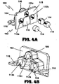
- the image sensor 70 and its associated lens as well as the IR LEDs 84a to 84c are mounted on a housing assembly 100 that is best illustrated in Figures 4a and 4b .
- the housing assembly 100 comprises a polycarbonate housing body 102 having a front portion 104 and a rear portion 106 extending from the front portion.
- An imaging aperture 108 is centrally formed in the housing body 102 and accommodates an IR-pass/visible light blocking filter 110.
- the filter 110 has an IR-pass wavelength range of between about 830nm and about 880nm.
- the image sensor 70 and associated lens are positioned behind the filter 110 and oriented such that the field of view of the image sensor 70 looks through the filter 110 and generally across the interactive surface 24.
- the rear portion 106 is shaped to surround the image sensor 70.
- Three passages 112a to 112c are formed through the housing body 102. Passages 112a and 112b are positioned on opposite sides of the filter 110 and are in general horizontal alignment with the image sensor 70. Passage 112c is centrally positioned above the filter 110.
- Each tubular passage receives a light source socket 114 that is configured to receive a respective one of the IR LEDs 84.
- the socket 114 received in passage 112a accommodates IR LED 84a
- the socket 114 received in passage 112b accommodates IR LED 84b
- the socket 114 received in passage 112c accommodates IR LED 84c.
- Mounting flanges 116 are provided on opposite sides of the rear portion 106 to facilitate connection of the housing assembly 100 to the bezel 26 via suitable fasteners.
- a label 118 formed of retro-reflective material overlies the front surface of the front portion 104.
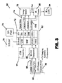
- master controller 50 comprises a DSP 200 such as that manufactured by Analog Devices under part number ADSP-BF522 Blackfin.
- a serial peripheral interface (SPI) flash memory 202 is connected to the DSP 200 via an SPI port and stores the firmware required for master controller operation.
- a synchronous dynamic random access memory (SDRAM) 204 that stores temporary data necessary for system operation is connected to the DSP 200 via an SDRAM port.
- the DSP 200 communicates with the general purpose computing device 28 over the USB cable 30 via a USB port.
- the DSP 200 communicates through its serial port (SPORT) with the imaging assemblies 60 via an RS-422 transceiver 208 over the differential synchronous signal (DSS) communication link 88.
- SPORT serial port
- DSS differential synchronous signal
- TDM time division multiplexed
- the DSP 200 also communicates with the imaging assemblies 60 via the RS-422 transceiver 208 over the synch line 90.
- DSP 200 communicates with the tool tray accessory module 48e over an inter-integrated circuit I 2 C channel and communicates with the communications accessory module 48f over universal asynchronous receiver/transmitter (UART), serial peripheral interface (SPI) and I 2 C channels.
- UART universal asynchronous receiver/transmitter
- SPI serial peripheral interface
- the general purpose computing device 160 in this embodiment is a computer comprising, for example, a processing unit, system memory (volatile and/or non-volatile memory), other non-removable or removable memory (eg. a hard disk drive, RAM, ROM, EEPROM, CD-ROM, DVD, flash memory, etc.) and a system bus coupling the various computer components to the processing unit.
- the computer may also comprise a network connection to access shared or remote drives, one or more networked computers, or other networked devices.
- the DSP 200 of the master controller 50 outputs synchronization signals that are applied to the synch line 90 via the transceiver 208.
- Each synchronization signal applied to the synch line 90 is received by the DSP 72 of each imaging assembly 60 via transceiver 86 and triggers a non-maskable interrupt (NMI) on the DSP 72.
- NMI non-maskable interrupt
- the DSP 72 of each imaging assembly 60 ensures that its local timers are within system tolerances and if not, corrects its local timers to match the master controller 50.
- the DSP 72 Using one local timer, the DSP 72 initiates a pulse sequence via the snapshot line that is used to condition the image sensor to the snapshot mode and to control the integration period and frame rate of the image sensor 70 in the snapshot mode.
- the DSP 72 also initiates a second local timer that is used to provide output on the LED control line 174 so that the IR LEDs 84a to 84c are properly powered during the image frame capture cycle.
- the image sensor 70 of each imaging assembly 60 acquires image frames at the desired image frame rate. In this manner, image frames captured by the image sensor 70 of each imaging assembly can be referenced to the same point of time allowing the position of pointers brought into the fields of view of the image sensors 70 to be accurately triangulated. Also, by distributing the synchronization signals for the imaging assemblies 60, electromagnetic interference is minimized by reducing the need for transmitting a fast clock signal to each image assembly 60 from the central location. Instead, each imaging assembly 60 has its own local oscillator (not shown) and a lower frequency signal (e.g. the point rate, 120Hz) is used to keep image frame capture synchronized
- a lower frequency signal e.g. the point rate, 120Hz
- the DSP 72 of each imaging assembly 60 also provides output to the strobe circuits 80 to control the switching of the IR LEDs 84a to 84c so that the IR LEDs are illuminated in a given sequence that is coordinated with the image frame capture sequence of each image sensor 70.
- the first image frame is captured by the image sensor 70 when the IR LED 84c is fully illuminated in a high current mode and the other IR LEDs are off.
- the next image frame is captured when all of the IR LEDs 84a to 84c are off. Capturing these successive image frames with the IR LED 84c on and then off allows ambient light artifacts in captured image frames to be cancelled by generating difference image frames as described in U.S.
- the third image frame is captured by the image sensor 70 when only the IR LED 84a is on and the fourth image frame is captured by the image sensor 70 when only the IR LED 84b is on. Capturing these image frames allows pointer edges and pointer shape to be determined as will be described.
- the strobe circuits 80 also control the IR LEDs 84a to 84c to inhibit blooming and to reduce the size of dark regions in captured image frames that are caused by the presence of other imaging assemblies 60 within the field of view of the image sensor 70.
- the IR LED 84 floods the region of interest over the interactive surface 24 with infrared illumination.
- Infrared illumination that impinges on the retro-reflective bands of bezel segments 40, 42, 44 and 46 and on the retro-reflective labels 118 of the housing assemblies 100 is returned to the imaging assemblies 60.
- the image sensor 70 of each imaging assembly 60 sees a bright band having a substantially even intensity over its length together with any ambient light artifacts.
- the pointer When a pointer is brought into proximity with the interactive surface 24, the pointer occludes infrared illumination reflected by the retro-reflective bands of bezel segments 40, 42, 44 and 46 and/or the retro-reflective labels 118. As a result, the image sensor 70 of each imaging assembly 60 sees a dark region that interrupts the bright band 159 in captured image frames. The reflections of the illuminated retro-reflective bands of bezel segments 40, 42, 44 and 46 and the illuminated retro-reflective labels 118 appearing on the interactive surface 24 are also visible to the image sensor 70.
- the IR LEDs 84 and the filter 110 of the other imaging assemblies 60 appear as dark regions that interrupt the bright band. These dark regions can be problematic as they can be inadvertently recognized as pointers.
- the image sensor 70 of one of the imaging assemblies 60 is capturing an image frame and its associated IR LEDs 84 are on, the IR strobe circuits 80 of the other imaging assemblies 60 are conditioned by the DSPs 72 to a low current mode.
- the strobe circuits 80 control the operating power supplied to the IR LEDs 84 so that they emit infrared backlighting at a level that is substantially equal to reflected illumination returned by the retro-reflective bands on the bezel segments 40, 42, 44 and 46 and retro-reflective labels 118. As a result, the size of each dark region is reduced. Operating the IR LEDs 84 in this manner also inhibits blooming (i.e. saturation of image sensor pixels) which can occur if the IR LEDs 84 of the other imaging assemblies 60 are fully on during image frame capture.
- the sequence of image frames captured by the image sensor 70 of each imaging assembly 60 is processed by the DSP 72 to identify each pointer in each image frame and to obtain pointer shape and contact information as will be described.
- the DSP 72 of each imaging assembly 60 in turn conveys the pointer data to the DSP 200 of the master controller 50.
- the DSP 200 uses the pointer data received from the DSPs 72 to calculate the position of each pointer relative to the interactive surface 24 in (x,y) coordinates using well known triangulation as described in above-incorporated U.S. Patent No. 6,803,906 to Morrison .
- This pointer coordinate data along with pointer shape and pointer contact status data is conveyed to the general purpose computing device 28 allowing the image data presented on the interactive surface 24 to be updated.
- the arrangement of the IR LEDs 84a to 84c employed by the imaging assemblies 60 may create shadows that appear in image frames as a pointer is brought proximate to the interactive surface 24 and into the fields of view of the image sensors 70.
- the IR LED 84c of an imaging assembly 60 that is conditioned to capture an image frame is illuminated, and a pointer is brought into proximity with the interactive surface 24, because the IR LED 84c is positioned above the image sensor 70 the pointer will cast a shadow that appears in the field of view of the image sensor 70 before the pointer actually makes contact with the interactive surface 24.
- the image frame captured by the image sensor 70 will include a dark region resulting from reflected backlight illumination that has been occluded by the pointer as well as a dark region corresponding to the shadow cast by the pointer on the bezel.
- the IR LED 84c is positioned above the image sensor 70, the shadow is cast from the higher and wider part of the pointer, and as a result, the dark region in the captured image frame resulting from the shadow will be dominate.
- the shape of the pointer tip and the contact status of the pointer relative to the interactive surface 24 will be obscured by the shadow. As will be appreciated, during image frame processing, this may result in early or false pointer contact detection for a pointer that is hovering over the interactive surface 24.
- Figure 6 is a representative image frame showing a pointer P being brought into proximity of the interactive surface 24 and the resulting shadow S (dotted lines) cast by the pointer when the IR LED 84c is illuminated.
- the shadow S dominates the image frame and appears in contact with the interactive surface 24.
- the shadow S also distorts the shape of the pointer P, in this case making the pointer appear larger than it actually is.
- the IR LEDs 84a and 84b are employed by each imaging assembly 60.
- Figure 7 is a top view of the interactive board 22 showing the IR LEDs 84a to 84c for only one of the imaging assemblies 60.
- the shadow cast by the pointer is to the right of the actual pointer. In this case, when the pointer is distant from the image sensor 70, the shadow cast by the pointer P overlaps with the pointer. When the pointer P is proximate to the image sensor 70, the shadow S cast by the pointer is spaced from the pointer P as shown in Figure 8 . Likewise, when the IR LED 84a is on during image frame capture, the shadow cast by the pointer P is to the left of the pointer. In this case, when the pointer is distant from the image sensor 70, the shadow cast by the pointer overlaps with the pointer.
- the shadow cast by the pointer is spaced from the pointer.
- the dark regions in captured image frames representing the pointer and the dark regions representing the shadows do not conflict allowing the shape of the pointer tip to be reliably detected.
- Pointer hover can also be differentiated from the cast shadows which extend to the interactive surface 24. As a result, the dark regions in the captured image frames representing the pointer allow the pointer shape and pointer contact status to be accurately determined.
- Figures 9a and 9b are captured image frames highlighting the scenario where the shadow S of the pointer P is very close to the pointer, which signifies that the pointer is far away from the imaging assembly 60 that captured the image frame.
- the pointer P is in contact with the interactive surface 24.
- Figures 10a and 10b are captured image frames highlighting the scenario where the pointer P hovers above the interactive surface 24. In this case, the pointer P is closer to the image sensor 70 and as a result the shadow S and actual pointer are moving apart.
- FIG 11 is a flowchart better illustrating the steps performed during image frame capture.
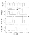
- the DSP 72 of each imaging assembly 60 conditions the image sensor 70 thereof to acquire a group of four (4) image frames in each image sensor exposure cycle with the IR LEDs 84a to 84c operated in the following sequence during image frame capture (step S1001):
- Figure 12 shows IR LED current and image sensor exposure timing diagrams for this operation sequence.
- each DSP 72 initially performs ambient light artifact cancellation by subtracting the image frame captured only with IR LED 84c on from the image frame captured with all IR LEDs off thereby to form a difference image frame that is devoid of ambient light artifacts (step S1002).
- the DSP 72 then examines the pixels of the difference image frame and computes a vertical intensity profile (VIP) for the difference image frame.
- the VIP comprises a single number for each column of the difference image frame. The number for each column provides an indication as to the presence of a pointer in the column of the difference image frame.
- the DSP 72 in turn performs continuity calculations to identify the pointer in the difference image frame and to determine an approximate location of the pointer in the difference image frame (step S1003).
- the DSP 72 compares the values of the pixels corresponding to the height of the retroreflective band to the values of an equal number of pixels above the retroreflective band. If no pointer is present then this comparison will reveal a high contrast result. If a pointer exists, whether bright or dark, the lighting will be approximately equal in both regions and the comparison will yield a low contrast result.
- each DSP 72 conveys the approximate pointer location information to the DSP 200 of the master controller 50 via the DSS communications link 88.
- the DSP 200 calculates an approximate position of the pointer relative to the interactive surface 24 in (x,y) coordinates using well known triangulation as described above (step S1004).
- the DSP 200 instructs the DSPs 72 of the imaging assemblies 60 to perform pointer edge and shape detection as well as to determine pointer contact status.
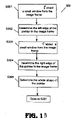
- each DSP 72 processes the image frame captured with only IR LED 84a on and the image frame captured only with IR LED 84b on to locate the pointer and its cast shadow in the image frames and to extract a window of image frame data therefrom that includes the pointer and its shadow (steps S301 and S303 in Figure 13 ).
- the extracted windows of image frame data are then analyzed to detect clear edges of the pointer.
- the pointer P is distorted in captured image frames by the cast shadows.
- the right edges of the pointer P in Figures 9a and 10a are overlapped with the cast shadows and the left edges of the pointer P in Figures 9b and 10b are overlapped with the cast shadows, resulting in unclear pointer edges that may possibly lead to pointer location inaccuracies. Therefore, using each pair of captured image frames, the left and right edges of the pointer can be determined.
- DSP 72 uses the image frame captured only when the IR LED 84b is on as shown in Figures 9a and 10a to determine the left edge of the pointer (step S302) since the left edge is not affected by a cast shadow and uses the image frame captured only when the IR LED 84a is on as shown in Figures 9b and 10b to determine the right edge of the pointer (step S304) since the right edge is not affected by a cast shadow.
- the DSP 72 determines the shape of the pointer (step S305).
- pointer contact status detection In order to determine pointer contact status relative to the interactive surface 24, one of two methods is employed.
- One of the methods for pointer contact status detection is similar to that disclosed in U.S. Patent No. 6,947,032 to Morrison et al. assigned to SMART Technologies ULC , the content of which is incorporated herein by reference in its entirety.
- the DSP 72 of each imaging assembly compares the pointer in the image frames with a reflection of the pointer in the image frames to determine if the pointer and its reflection are touching. If so, the pointer is determined to be in contact with the interactive surface 24 and if not, the pointer is determined to be hovering over the interactive surface.
- An alternate method is to find a path from the top of the bezel to the bottom of the reflection of the bezel in each image frame (step S201 in Figure 14 ). If there is no path from the top of the bezel to the bottom of the bezel reflection in the image frame as shown in Figure 15A , pointer hover is detected (step S202). If there is a path from the top of the bezel to the bottom of the bezel reflection in the image frame as shown in Figure 15B , pointer contact with the interactive surface 24 is detected (step S203).
- pointer contact is detected at step S203 by a DSP 72, the approximate location of the pointer contact in the image frame is reevaluated. Initially, the location of pointer contact is assumed to be on the centerline of the dark region representing the pointer in the captured image frames. However, the image frames are sometimes distorted due to tilt of the pointer as also shown in Figures 15A and 15B . In this case, it is necessary to find the actual pointer contact location. Therefore, at step S204, the DSP 72 detects if there is an offset t between the centerline of the pointer and the center of the narrowest part of the pointer in the captured image frame. If there is no offset t, the pointer is considered to be perpendicular to the interactive surface 24.
- step S1003 no adjust to the approximate pointer location calculated at step S1003 is required as this calculated pointer location is the actual pointer location (step S205). If there is an offset t, the pointer is determined to be tilted. The approximate pointer location calculated at step S1003 is then adjusted to correspond to the center of the narrowest part of the pointer in the image frame (step S206) and the adjusted pointer location is transmitted to the DSP 200.
- the DSP 200 uses the adjusted pointer locations to triangulate and recalculate the pointer contact coordinates relative to the interactive surface 24. In this way, accurate contact status and pointer locations relative to the interactive surface 24 in (x,y) coordinates can be determined.
- imaging assemblies 60 are shown as comprising three IR LEDs, fewer IR LEDs may be employed.
- Figure 16 shows an imaging assembly comprising only two IR LEDs 48b and 48c. Similar to the previous embodiment, both IR LEDs are used to provide backlight illumination during each image sensor exposure sequence.
- the image frames are processed in a manner similar to that described above to determine pointer hover or contact.
- the distance between the pointer and its shadow in captured image frames defined as shadow offset
- the distance from the image sensor 70 to the pointer can be estimated.
- the calculation for the shadow offset will now be described.
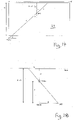
- the geometry of the interactive surface 24 is shown in Figures 17 and 18 .
- the first step of the shadow offset calculation is to compute the image sensor-bezel distance.
- the interactive surface 24 is assumed to have a known height H and width W.
- the image sensor-bezel distance is d + D.
- the shadow offset x s is a function of the pointer to image sensor distance d and also a function of the pointer to bezel distance D. The geometry for their relationship is shown in Figure 17 .
- the IR LEDs 48b and 48c for each imaging assembly 60 can be controlled in one of two ways during each image sensor exposure sequence.
- the image sensor 70 of each imaging assembly 60 is conditioned to acquire a group of three (3) image frames in each exposure cycle with the IR LEDs 84b and 84c operated in the following sequence:
- Figure 19 shows IR LED current and image sensor exposure timing diagrams for this operation sequence.
- the other method is to modulate both LEDs simultaneously with two different Walsh codes.
- This technique is disclosed in U.S. Patent Application Publication No. 2009-0278794 to McGibney et al. entitled “Interactive Input System with Controlled Lighting” filed on May 9, 2008 , assigned to SMART Technologies, ULC of Calgary, Alberta, Canada, assignee of the subject application, the content of which is incorporated herein by reference in its entirety.
- each DSP 72 initially performs ambient light artifact cancellation by subtracting the image frame captured only with IR LED 84c on from the image frame captured with both IR LEDs off thereby to form a difference image frame that is devoid of ambient light artifacts.
- the DSP 72 then examines the pixels of the difference image frame and computes the vertical intensity profile (VIP) for the difference image frame and performs the continuity calculations as described above to identify the pointer in the difference image frame and to determine an approximate location of the pointer in the difference image frame.
- VIP vertical intensity profile
- each DSP 72 conveys the pointer location information to the DSP 200 of the master controller 50 via the DSS communications link 88. Transmission of the pointer location information to the DSP 200 is performed at a reduced frame rate (nominally 120 frames per second).
- the DSP 72 calculates the shadow offset x s for the image frames generated by the imaging assemblies. For each image frame, if the shadow offset x s is greater than a threshold, signifying that the shadow of the pointer is totally separated from the pointer, the DSP extracts a window of the difference image frame that includes the pointer and its shadow and proceeds to step S201 shown in Figure 14 . If the shadow offset x s is less than the threshold, signifying that the shadow of the pointer overlaps with the pointer, the DSP extracts a window of a difference image frame resulting from the subtraction of the image frame captured with IR LEDs 48b and 48c off from the image frame captured with IR LED 48b on and then proceeds to step S201.
- the IR LED light sources 82 are described as operating in a low current mode during the entire camera synchronization signal, one of ordinary skill in the art will appreciate that the low current mode duration may be reduced.
- feedback is not used to control the illumination of the IR light sources 82, one of ordinary skill in the art will appreciate that feedback may be employed to match the IR light source illumination to the intensity of illumination reflected by the retro-reflective bezel. In order to do so, the image frames captured by the imaging assemblies 60 can be used to adjust the brightness (eg. the current) of the opposing IR illumination sources. Such feedback may be advantageous to reduce the complexity of the image processing algorithms.
- calibration may be necessary in order to match the brightness of the IR illumination sources to the retro-reflective bezel.
- the calibration may be performed manually or automatically using feedback from the opposing imaging assemblies.
- the brightnesses of the IR illumination sources do not precisely have to match the intensity of illumination reflected by the retro-reflective bezel.
- processors located at each imaging assembly
- processors could be used to achieve the same results.
- the processor is not limited to a DSP but could be a general purpose processor, microcontroller, or other processing device.
- the processor could also be integrated into the imaging sensor.
- the frame rate of the imaging assemblies is 960Hz, as mentioned previously, the interactive input system is not limited to these frequencies.
- the image sensors of the imaging assemblies may be capable of very high frame rates, such as those on the order of 10 6 frames per second, or very low frame rates, such as 30 frames per second.
- very high frame rates such as those on the order of 10 6 frames per second
- very low frame rates such as 30 frames per second.
- the imaging assemblies 60 are described as communicating with the master controller 50 via a DSS communication link.
- Other communication links such as a parallel bus, a universal serial bus (USB), an Ethernet connection or other suitable wired connection may however be employed.
- the imaging assemblies 22 may communicate with the master controller 50 over a wireless connection using a suitable wireless protocol such as for example Bluetooth, WiFi, ZigBee, ANT, IEEE 802.15.4, Z-Wave etc.
- the master controller 50 is described as communicating with the general purpose computing device 28 via a USB cable 30.
- the master controller 50 may communicate with the general purpose computing device 28 over another wired connection such as for example, a parallel bus, an RS-232 connection, an Ethernet connection etc. or may communicate with the general purpose computing device 28 over a wireless connection using a suitable wireless protocol such as for example Bluetooth, WiFi, ZigBee, ANT, IEEE 802.15.4, Z-Wave etc.
Landscapes
- Engineering & Computer Science (AREA)
- General Engineering & Computer Science (AREA)
- Theoretical Computer Science (AREA)
- Human Computer Interaction (AREA)
- Physics & Mathematics (AREA)
- General Physics & Mathematics (AREA)
- Studio Devices (AREA)
- Position Input By Displaying (AREA)
Description
- The present invention relates to an interactive input system and to an illumination method therefor.
- Interactive input systems that allow users to inject input (e.g. digital ink, mouse events, etc.) into an application program using an active pointer (eg. a pointer that emits light, sound or other signal), a passive pointer (eg. a finger, cylinder or other object) or other suitable input device such as for example, a mouse or trackball, are well known. These interactive input systems include but are not limited to: touch systems comprising touch panels employing analog resistive or machine vision technology to register pointer input such as those disclosed in
U.S. Patent Nos. 5,448,263 ;6,141,000 ;6,337,681 ;6,747,636 ;6,803,906 ;7,232,986 ;7,236,162 ;7,274,356 ; and7,532,206 assigned to SMART Technologies ULC of Calgary, Alberta, Canada, assignee of the subject application, the contents of which are incorporated by reference in their entirety; touch systems comprising touch panels employing electromagnetic, capacitive, acoustic or other technologies to register pointer input; tablet personal computers (PCs); laptop PCs; personal digital assistants (PDAs); and other similar devices. - Above-incorporated
U.S. Patent No. 6,803,906 to Morrison et al. discloses a touch system that employs machine vision to detect pointer interaction with a touch surface on which a computer-generated image is presented. A rectangular bezel or frame surrounds the touch surface and supports digital imaging devices at its corners. The digital imaging devices have overlapping fields of view that encompass and look generally across the touch surface. The digital imaging devices acquire images looking across the touch surface from different vantages and generate image data. Image data acquired by the digital imaging devices is processed by on-board digital signal processors to determine if a pointer exists in the captured image data. When it is determined that a pointer exists in the captured image data, the digital signal processors convey pointer characteristic data to a master controller, which in turn processes the pointer characteristic data to determine the location of the pointer in (x,y) coordinates relative to the touch surface using triangulation. The pointer coordinates are conveyed to a computer executing one or more application programs. The computer uses the pointer coordinates to update the computer-generated image that is presented on the touch surface. Pointer contacts on the touch surface can therefore be recorded as writing or drawing or used to control execution of application programs executed by the computer. - Above-incorporated
U.S. Patent No. 7,232,986 to Worthington et al. , discloses a camera-based touch system comprising a bezel that is illuminated by at least one light source, such as an array of infrared (IR) light emitting diodes (LEDs). Each light source is associated with and positioned adjacent each camera. The bezel reflects infrared light emitted by the at least one light source back towards the cameras. As a result, each camera sees a bright band of illumination within its field of view. When a pointer is positioned within the fields of view of the cameras, the pointer occludes the infrared illumination and therefore appears as a high-contrast dark region interrupting the bright band of illumination in each captured image allowing the existence of the pointer in captured images to be readily detected. -
U.S. Patent Application Publication No. 2009/0058833 to Newton discloses an optical touch screen comprising a primary illumination source, a secondary illumination source and retro-reflective components positioned along the edge of the touch screen to reflect light, providing backlight to a light detection system. The primary illumination source (eg. a set of LEDs or diodes) emits light in a fan-shaped pattern with its apex aligned with the optical center of the detection system; while the secondary illumination source is not aligned with the optical center of the detection system. When an object is present, its position can be triangulated based on the direction of its shadow at the detection system. -
U.S. Patent Application Publication No. 2009/0213093 to Bridger discloses an optical position sensing system including a plurality of radiation sources. The position of the radiation sources may be varied with respect to the aperture to achieve performance enhancement. Supplemental radiation sources may be positioned around the bezel so as to provide supplemental backlighting. Each of the plurality of supplemental radiation sources can be individually activated and deactivated, so as to selectively provide the supplemental backlighting to selected areas within the bezel. -
U.S. Patent Application Publication No. 2009/0213094 to Bridger discloses an optical position sensing assembly including a body. An optical sensor is mounted to a rear face of the body and a radiation source is positioned within the body above the lens. A light path separator is positioned between the radiation source and an image window for the optical sensor, so that the radiation path is optically separated from the view path of the optical sensor. -
US2003/0085871 describes an interactive input system comprising a plurality of imaging devices in which each imaging device is provided with a pair of infrared light emitting diodes arranged on either side of the imaging device. -
WO2005/031554 describes a variety of possible illumination arrangements. A first embodiment comprises a pair of detection units, wherein each detection unit comprises a single light source provided above a slit and imaging sensor. An alternative embodiment comprises a pair of light sources that provide light into respective mirrors in order to emit the light as close as possible to the detection surface. Since left and right light sources are provided a centre of the shadow of the pointer can be used to triangulate the pointer position. A further embodiment comprises a pair of detection units, one on each top corner. Each detection unit comprises a single light source. Different detection units are used to determine different sides of a pointer. -
JP2002132435 -
WO2009135320 teaches of an interactive input system in which a controller processes successive image frames output by the image sensor of each imaging assembly in pairs. In particular, when one image frame is received, the controller stores the image frame in a buffer. When the successive image frame is received, the controller similarly stores the image frame in a buffer. With the successive image frames available, the controller subtracts the two image frames to form a difference image frame. Provided the frame rates of the image sensors are high enough, ambient light levels in successive image frames will typically not change significantly and as a result, ambient light is substantially cancelled out and does not appear in the difference image frame. - Although the above-mentioned interactive input systems allow pointer contacts with the touch surfaces to be determined, in interactive input systems that employ retro-reflective material to return backlighting to imaging assemblies, a pointer may in certain circumstances cast a shadow that appears in captured image frames. Depending on the nature of the shadow, the shadow may be inadvertently detected as a pointer contact.
- It is therefore an object of the present invention to provide a novel interactive input system and a novel method of reducing shadow pointer effects employed by the interactive input system.
- Accordingly, in one aspect there is provided an illumination assembly for an interactive input system in accordance with
independent claim 1. - In one embodiment, the one illumination source is generally vertically aligned with the at least one imaging device and is positioned above the at least one imaging device. At least one other illumination source is positioned to one side the imaging device and is in generally the same plane as the at least one imaging device. In another embodiment, at least one other illumination source is positioned on each side of the imaging device.
- In one embodiment, the controller conditions the illumination sources so that for an exposure cycle of the at least one imaging assembly, the imaging assembly captures an image frame with each illumination source on and the other illumination sources off and an image frame with all illumination sources off. In one embodiment, the illumination sources are infrared (IR) illumination sources.
- According to another aspect there is provided a method in accordance with independent claim 5.
- Embodiments will now be described more fully with reference to the accompanying drawings in which:
-
Figure 1 is a schematic, partial perspective view of an interactive input system; -
Figure 2 is a block diagram of the interactive input system ofFigure 1 ; -
Figure 3 is a block diagram of an imaging assembly forming part of the interactive input system ofFigure 1 ; -
Figures 4a and 4b are front and rear perspective views of a housing assembly forming part of the imaging assembly ofFigure 3 ; -
Figure 5 is a block diagram of a master controller forming part of the interactive input system ofFigure 1 ; -
Figure 6 is an exemplary image frame captured by the imaging assembly ofFigure 3 comprising a pointer and a pointer shadow; -
Figure 7 is a top plan view of a portion of the interactive input system ofFigure 1 ; -
Figure 8 is another exemplary image frame captured by the imaging assembly ofFigure 3 comprising a pointer and a pointer shadow; -
Figures 9A and 9B are further exemplary image frames captured by the imaging assembly ofFigure 3 comprising pointers and pointer shadows; -
Figures 10A and 10B are still further exemplary image frames captured by the imaging assembly ofFigure 3 comprising pointers and pointer shadows; -
Figure 11 is a flowchart showing steps performed during processing of image frames captured by imaging assemblies of the interactive input system ofFigure 1 ; -
Figure 12 shows illumination source current and image sensor exposure timing diagrams for the interactive input system ofFigure 1 ; -
Figures 13 and14 are flowcharts showing steps performed during processing of image frames captured by imaging assemblies of the interactive input system ofFigure 1 ; -
Figures 15A and 15B are exemplary image frames captured by the imaging assembly ofFigure 3 comprising a bezel and its reflection together with a pointer and its reflection; -
Figure 16 is a top plan view of a portion of an alternative example of an interactive input system not forming part of the invention; -
Figures 17 and 18 are top plan views showing geometries of the alternative example interactive input system ofFigure 16 not forming part of the invention; ; and -
Figure 19 shows illumination source current and image sensor exposure timing diagrams for the example interactive input system ofFigure 16 not forming part of the invention. - Turning now to
Figures 1 and2 , an interactive input system that allows a user to inject input such as digital ink, mouse events etc. into an application program executed by a computing device is shown and is generally identified byreference numeral 20. In this embodiment,interactive input system 20 comprises aninteractive board 22 mounted on a vertical support surface such as for example, a wall surface or the like.Interactive board 22 comprises a generally planar, rectangularinteractive surface 24 that is surrounded about its periphery by abezel 26. An ultra-short throw projector (not shown) such as that sold by SMART Technologies ULC under the name SMART UX60 is also mounted on the support surface above theinteractive board 22 and projects an image, such as for example a computer desktop, onto theinteractive surface 24. - The
interactive board 22 employs machine vision to detect one or more pointers brought into a region of interest in proximity with theinteractive surface 24. Theinteractive board 22 communicates with a generalpurpose computing device 28 executing one or more application programs via a universal serial bus (USB)cable 30. Generalpurpose computing device 28 processes the output of theinteractive board 22 and adjusts image data that is output to the projector, if required, so that the image presented on theinteractive surface 24 reflects pointer activity. In this manner, theinteractive board 22, generalpurpose computing device 28 and projector allow pointer activity proximate to theinteractive surface 24 to be recorded as writing or drawing or used to control execution of one or more application programs executed by the generalpurpose computing device 28. - The
bezel 26 in this embodiment is mechanically fastened to theinteractive surface 24 and comprises fourbezel segments Bezel segments interactive surface 24 whilebezel segments interactive surface 24 respectively. In this embodiment, the inwardly facing surface of eachbezel segment bezel segments interactive surface 24. - A
tool tray 48 is affixed to theinteractive board 22 adjacent thebezel segment 46 using suitable fasteners such as for example, screws, clips, adhesive etc. As can be seen, thetool tray 48 comprises ahousing 48a having anupper surface 48b configured to define a plurality of receptacles orslots 48c. Thereceptacles 48c are sized to receive pen tools and an eraser tool (not shown) that can be used to interact with theinteractive surface 24.Control buttons 48d are provided on theupper surface 48b to enable a user to control operation of theinteractive input system 20. One end of thetool tray 48 is configured to receive a detachable tooltray accessory module 48e while the opposite end of thetool tray 48 is configured to receive adetachable communications module 48f for remote device communications. Thehousing 48a accommodates a master controller 50 (seeFigure 5 ) as will be described. Further specifics of thetool tray 48 are described in co-pendingU.S. Application Serial No. 12/709,424 to Bolt et al. entitled "INTERACTIVE INPUT SYSTEM AND PEN TOOL TRAY THEREFOR" filed on February 19, 2010 -
Imaging assemblies 60 are accommodated by thebezel 26, with eachimaging assembly 60 being positioned adjacent a different corner of the bezel. Theimaging assemblies 60 are oriented so that their fields of view overlap and look generally across the entireinteractive surface 24. In this manner, any pointer such as for example a user's finger, a cylinder or other suitable object, or a pen or eraser tool lifted from areceptacle 48c of thetool tray 48, that is brought into proximity of theinteractive surface 24 appears in the fields of view of theimaging assemblies 60. Apower adapter 62 provides the necessary operating power to theinteractive board 22 when connected to a conventional AC mains power supply. - Turning now to
Figure 3 , one of theimaging assemblies 60 is better illustrated. As can be seen, theimaging assembly 60 comprises animage sensor 70 such as that manufactured by Aptina (Micron) MT9V034 having a resolution of 752x480 pixels, fitted with a two element, plastic lens (not shown) that provides theimage sensor 70 with a field of view of approximately 104 degrees. In this manner, theother imaging assemblies 60 are within the field of view of theimage sensor 70 thereby to ensure that the field of view of theimage sensor 70 encompasses the entireinteractive surface 24. - A digital signal processor (DSP) 72 such as that manufactured by Analog Devices under part number ADSP-BF522 Blackfin or other suitable processing device, communicates with the
image sensor 70 over animage data bus 74 via a parallel port interface (PPI). A serial peripheral interface (SPI)flash memory 74 is connected to theDSP 72 via an SPI port and stores the firmware required for image assembly operation. Depending on the size of captured image frames as well as the processing requirements of theDSP 72, theimaging assembly 60 may optionally comprise synchronous dynamic random access memory (SDRAM) 76 to store additional temporary data as shown by the dotted lines. Theimage sensor 70 also communicates with theDSP 72 via a a two-wire interface (TWI) and a timer (TMR) interface. The control registers of theimage sensor 70 are written from theDSP 72 via the TWI in order to configure parameters of theimage sensor 70 such as the integration period for theimage sensor 70. - In this embodiment, the
image sensor 70 operates in snapshot mode. In the snapshot mode, theimage sensor 70, in response to an external trigger signal received from theDSP 72 via the TMR interface that has a duration set by a timer on theDSP 72, enters an integration period during which an image frame is captured. Following the integration period after the generation of the trigger signal by theDSP 72 has ended, theimage sensor 70 enters a readout period during which time the captured image frame is available. With the image sensor in the readout period, theDSP 72 reads the image frame data acquired by theimage sensor 70 over theimage data bus 74 via the PPI. The frame rate of theimage sensor 70 in this embodiment is between about 900 and about 960 frames per second. TheDSP 72 in turn processes image frames received from theimage sensor 72 and provides pointer information to themaster controller 50 at a reduced rate of approximately 120 points/sec. Those of skill in the art will however appreciate that other frame rates may be employed depending on the desired accuracy of pointer tracking and whether multi-touch and/or active pointer identification is employed. - Three
IR strobe circuits 80 communicate with theDSP 72 via the TWI and via a general purpose input/output (GPIO) interface. TheIR strobe circuits 80 also communicate with theimage sensor 70 and receive power provided onLED power line 82 via the power adapter 52. EachIR strobe circuit 80 drives a respective illumination source in the form of infrared (IR) light emitting diode (LEDs) 84a to 84c that provides infrared backlighting over theinteractive surface 24 for theimaging assembly 60 during image capture. - The
DSP 72 also communicates with an RS-422transceiver 86 via a serial port (SPORT) and a non-maskable interrupt (NMI) port. Thetransceiver 86 communicates with themaster controller 50 over a differential synchronous signal (DSS)communication link 88 and asynch line 90. Power for the components of theimaging assembly 60 is provided onpower line 92 by the power adapter 52.DSP 72 may also optionally be connected to aUSB connector 94 via a USB port as indicated by the dotted lines. TheUSB connector 94 can be used to connect theimaging assembly 60 to diagnostic equipment. Further, by using a similar architecture for both theimaging assembly 60 and themaster controller 50, the same circuit board assembly and common components may be used for both thus reducing the part count and cost of the interactive input system. Differing components are added to the circuit board assemblies during manufacture dependent upon whether the circuit board assembly is intending for use in animaging assembly 60 or in themaster controller 50. For example, themaster controller 50 may require aSRAM 76 whereas theimaging assembly 60 may not. - The
image sensor 70 and its associated lens as well as the IR LEDs 84a to 84c are mounted on ahousing assembly 100 that is best illustrated inFigures 4a and 4b . As can be seen, thehousing assembly 100 comprises apolycarbonate housing body 102 having afront portion 104 and arear portion 106 extending from the front portion. Animaging aperture 108 is centrally formed in thehousing body 102 and accommodates an IR-pass/visiblelight blocking filter 110. Thefilter 110 has an IR-pass wavelength range of between about 830nm and about 880nm. Theimage sensor 70 and associated lens are positioned behind thefilter 110 and oriented such that the field of view of theimage sensor 70 looks through thefilter 110 and generally across theinteractive surface 24. Therear portion 106 is shaped to surround theimage sensor 70. Threepassages 112a to 112c are formed through thehousing body 102.Passages filter 110 and are in general horizontal alignment with theimage sensor 70.Passage 112c is centrally positioned above thefilter 110. Each tubular passage receives alight source socket 114 that is configured to receive a respective one of theIR LEDs 84. In particular, thesocket 114 received inpassage 112a accommodates IR LED 84a, thesocket 114 received inpassage 112b accommodates IR LED 84b, and thesocket 114 received inpassage 112c accommodates IR LED 84c. Mountingflanges 116 are provided on opposite sides of therear portion 106 to facilitate connection of thehousing assembly 100 to thebezel 26 via suitable fasteners. Alabel 118 formed of retro-reflective material overlies the front surface of thefront portion 104. Further specifics concerning the housing assembly and its method of manufacture are described in co-pendingU.S. Application Serial No. 12/709,419 to Liu et al. entitled "HOUSING ASSEMBLY FOR INTERACTIVE INPUT SYSTEM AND FABRICATION METHOD" filed on February 19, 2010 - Turning now to
Figure 5 , themaster controller 50 is better illustrated. As can be seen,master controller 50 comprises aDSP 200 such as that manufactured by Analog Devices under part number ADSP-BF522 Blackfin. A serial peripheral interface (SPI)flash memory 202 is connected to theDSP 200 via an SPI port and stores the firmware required for master controller operation. A synchronous dynamic random access memory (SDRAM) 204 that stores temporary data necessary for system operation is connected to theDSP 200 via an SDRAM port. TheDSP 200 communicates with the generalpurpose computing device 28 over theUSB cable 30 via a USB port. TheDSP 200 communicates through its serial port (SPORT) with theimaging assemblies 60 via an RS-422transceiver 208 over the differential synchronous signal (DSS)communication link 88. In this embodiment, as more than oneimaging assembly 60 communicates with themaster controller DSP 200 over theDSS communication link 88, time division multiplexed (TDM) communications is employed. TheDSP 200 also communicates with theimaging assemblies 60 via the RS-422transceiver 208 over thesynch line 90.DSP 200 communicates with the tooltray accessory module 48e over an inter-integrated circuit I2C channel and communicates with thecommunications accessory module 48f over universal asynchronous receiver/transmitter (UART), serial peripheral interface (SPI) and I2C channels. - The general purpose computing device 160 in this embodiment is a computer comprising, for example, a processing unit, system memory (volatile and/or non-volatile memory), other non-removable or removable memory (eg. a hard disk drive, RAM, ROM, EEPROM, CD-ROM, DVD, flash memory, etc.) and a system bus coupling the various computer components to the processing unit. The computer may also comprise a network connection to access shared or remote drives, one or more networked computers, or other networked devices.
- During operation, the
DSP 200 of themaster controller 50 outputs synchronization signals that are applied to thesynch line 90 via thetransceiver 208. Each synchronization signal applied to thesynch line 90 is received by theDSP 72 of eachimaging assembly 60 viatransceiver 86 and triggers a non-maskable interrupt (NMI) on theDSP 72. In response to the non-maskable interrupt triggered by the synchronization signal, theDSP 72 of eachimaging assembly 60 ensures that its local timers are within system tolerances and if not, corrects its local timers to match themaster controller 50. Using one local timer, theDSP 72 initiates a pulse sequence via the snapshot line that is used to condition the image sensor to the snapshot mode and to control the integration period and frame rate of theimage sensor 70 in the snapshot mode. TheDSP 72 also initiates a second local timer that is used to provide output on theLED control line 174 so that the IR LEDs 84a to 84c are properly powered during the image frame capture cycle. - In response to the initiated pulse sequence, the
image sensor 70 of eachimaging assembly 60 acquires image frames at the desired image frame rate. In this manner, image frames captured by theimage sensor 70 of each imaging assembly can be referenced to the same point of time allowing the position of pointers brought into the fields of view of theimage sensors 70 to be accurately triangulated. Also, by distributing the synchronization signals for theimaging assemblies 60, electromagnetic interference is minimized by reducing the need for transmitting a fast clock signal to eachimage assembly 60 from the central location. Instead, eachimaging assembly 60 has its own local oscillator (not shown) and a lower frequency signal (e.g. the point rate, 120Hz) is used to keep image frame capture synchronized - During image frame capture, the
DSP 72 of eachimaging assembly 60 also provides output to thestrobe circuits 80 to control the switching of the IR LEDs 84a to 84c so that the IR LEDs are illuminated in a given sequence that is coordinated with the image frame capture sequence of eachimage sensor 70. In particular, in the sequence the first image frame is captured by theimage sensor 70 when the IR LED 84c is fully illuminated in a high current mode and the other IR LEDs are off. The next image frame is captured when all of the IR LEDs 84a to 84c are off. Capturing these successive image frames with the IR LED 84c on and then off allows ambient light artifacts in captured image frames to be cancelled by generating difference image frames as described inU.S. Application Publication No. 2009/0278794 to McReynolds et al., assigned to SMART Technologies ULC , the content of which is incorporated herein by reference in its entirety. The third image frame is captured by theimage sensor 70 when only the IR LED 84a is on and the fourth image frame is captured by theimage sensor 70 when only the IR LED 84b is on. Capturing these image frames allows pointer edges and pointer shape to be determined as will be described. Thestrobe circuits 80 also control the IR LEDs 84a to 84c to inhibit blooming and to reduce the size of dark regions in captured image frames that are caused by the presence ofother imaging assemblies 60 within the field of view of theimage sensor 70. - During the image capture sequence, when each
IR LED 84 is on, the IR LED floods the region of interest over theinteractive surface 24 with infrared illumination. Infrared illumination that impinges on the retro-reflective bands ofbezel segments reflective labels 118 of thehousing assemblies 100 is returned to theimaging assemblies 60. As a result, in the absence of a pointer, theimage sensor 70 of eachimaging assembly 60 sees a bright band having a substantially even intensity over its length together with any ambient light artifacts. When a pointer is brought into proximity with theinteractive surface 24, the pointer occludes infrared illumination reflected by the retro-reflective bands ofbezel segments reflective labels 118. As a result, theimage sensor 70 of eachimaging assembly 60 sees a dark region that interrupts the bright band 159 in captured image frames. The reflections of the illuminated retro-reflective bands ofbezel segments reflective labels 118 appearing on theinteractive surface 24 are also visible to theimage sensor 70. - When an image frame is captured by the
image sensor 70 of one of theimaging assemblies 60 when theIR LEDs 84 associated with theother imaging assemblies 60 are off during image frame capture, theIR LEDs 84 and thefilter 110 of theother imaging assemblies 60 appear as dark regions that interrupt the bright band. These dark regions can be problematic as they can be inadvertently recognized as pointers. To address this problem, when theimage sensor 70 of one of theimaging assemblies 60 is capturing an image frame and its associatedIR LEDs 84 are on, theIR strobe circuits 80 of theother imaging assemblies 60 are conditioned by theDSPs 72 to a low current mode. In the low current mode, thestrobe circuits 80 control the operating power supplied to theIR LEDs 84 so that they emit infrared backlighting at a level that is substantially equal to reflected illumination returned by the retro-reflective bands on thebezel segments reflective labels 118. As a result, the size of each dark region is reduced. Operating theIR LEDs 84 in this manner also inhibits blooming (i.e. saturation of image sensor pixels) which can occur if theIR LEDs 84 of theother imaging assemblies 60 are fully on during image frame capture. - The sequence of image frames captured by the
image sensor 70 of eachimaging assembly 60 is processed by theDSP 72 to identify each pointer in each image frame and to obtain pointer shape and contact information as will be described. TheDSP 72 of eachimaging assembly 60 in turn conveys the pointer data to theDSP 200 of themaster controller 50. TheDSP 200 uses the pointer data received from theDSPs 72 to calculate the position of each pointer relative to theinteractive surface 24 in (x,y) coordinates using well known triangulation as described in above-incorporatedU.S. Patent No. 6,803,906 to Morrison . This pointer coordinate data along with pointer shape and pointer contact status data is conveyed to the generalpurpose computing device 28 allowing the image data presented on theinteractive surface 24 to be updated. - The arrangement of the IR LEDs 84a to 84c employed by the
imaging assemblies 60 may create shadows that appear in image frames as a pointer is brought proximate to theinteractive surface 24 and into the fields of view of theimage sensors 70. For example, when the IR LED 84c of animaging assembly 60 that is conditioned to capture an image frame is illuminated, and a pointer is brought into proximity with theinteractive surface 24, because the IR LED 84c is positioned above theimage sensor 70 the pointer will cast a shadow that appears in the field of view of theimage sensor 70 before the pointer actually makes contact with theinteractive surface 24. In this case, the image frame captured by theimage sensor 70 will include a dark region resulting from reflected backlight illumination that has been occluded by the pointer as well as a dark region corresponding to the shadow cast by the pointer on the bezel. Also, since the IR LED 84c is positioned above theimage sensor 70, the shadow is cast from the higher and wider part of the pointer, and as a result, the dark region in the captured image frame resulting from the shadow will be dominate. In this case, the shape of the pointer tip and the contact status of the pointer relative to theinteractive surface 24 will be obscured by the shadow. As will be appreciated, during image frame processing, this may result in early or false pointer contact detection for a pointer that is hovering over theinteractive surface 24. For example,Figure 6 is a representative image frame showing a pointer P being brought into proximity of theinteractive surface 24 and the resulting shadow S (dotted lines) cast by the pointer when the IR LED 84c is illuminated. As can be seen, in this situation, although the pointer P is not in contact with theinteractive surface 24, the shadow S dominates the image frame and appears in contact with theinteractive surface 24. The shadow S also distorts the shape of the pointer P, in this case making the pointer appear larger than it actually is. - In order to improve the visualization of a pointer brought into proximity of the
interactive surface 24 and to make the pointer contact detect and pointer type identification more reliable, the IR LEDs 84a and 84b are employed by eachimaging assembly 60.Figure 7 is a top view of theinteractive board 22 showing the IR LEDs 84a to 84c for only one of theimaging assemblies 60. - When the IR LED 84b is on during image frame capture, the shadow cast by the pointer is to the right of the actual pointer. In this case, when the pointer is distant from the
image sensor 70, the shadow cast by the pointer P overlaps with the pointer. When the pointer P is proximate to theimage sensor 70, the shadow S cast by the pointer is spaced from the pointer P as shown inFigure 8 . Likewise, when the IR LED 84a is on during image frame capture, the shadow cast by the pointer P is to the left of the pointer. In this case, when the pointer is distant from theimage sensor 70, the shadow cast by the pointer overlaps with the pointer. When the pointer P is proximate to theimage sensor 70, the shadow cast by the pointer is spaced from the pointer. In scenarios where the shadows are spaced from the pointers, the dark regions in captured image frames representing the pointer and the dark regions representing the shadows do not conflict allowing the shape of the pointer tip to be reliably detected. Pointer hover can also be differentiated from the cast shadows which extend to theinteractive surface 24. As a result, the dark regions in the captured image frames representing the pointer allow the pointer shape and pointer contact status to be accurately determined. -
Figures 9a and 9b are captured image frames highlighting the scenario where the shadow S of the pointer P is very close to the pointer, which signifies that the pointer is far away from theimaging assembly 60 that captured the image frame. In this example, the pointer P is in contact with theinteractive surface 24.Figures 10a and 10b are captured image frames highlighting the scenario where the pointer P hovers above theinteractive surface 24. In this case, the pointer P is closer to theimage sensor 70 and as a result the shadow S and actual pointer are moving apart. -
Figure 11 is a flowchart better illustrating the steps performed during image frame capture. As previously mentioned, theDSP 72 of eachimaging assembly 60 conditions theimage sensor 70 thereof to acquire a group of four (4) image frames in each image sensor exposure cycle with the IR LEDs 84a to 84c operated in the following sequence during image frame capture (step S1001): - (1) only IR LED 84c on;
- (2) all IR LEDs off;
- (3) only IR LED 84a on; and
- (4) only IR LED 84b on.
-
Figure 12 shows IR LED current and image sensor exposure timing diagrams for this operation sequence. - The image frames captured by each
image sensor 70 over each exposure cycle are conveyed to its associatedDSP 72. In response to the received image frames, eachDSP 72 initially performs ambient light artifact cancellation by subtracting the image frame captured only with IR LED 84c on from the image frame captured with all IR LEDs off thereby to form a difference image frame that is devoid of ambient light artifacts (step S1002). TheDSP 72 then examines the pixels of the difference image frame and computes a vertical intensity profile (VIP) for the difference image frame. The VIP comprises a single number for each column of the difference image frame. The number for each column provides an indication as to the presence of a pointer in the column of the difference image frame. TheDSP 72 in turn performs continuity calculations to identify the pointer in the difference image frame and to determine an approximate location of the pointer in the difference image frame (step S1003). During the continuity calculations, for the columns of the difference image frame where the pointer is believed to exist, theDSP 72 compares the values of the pixels corresponding to the height of the retroreflective band to the values of an equal number of pixels above the retroreflective band. If no pointer is present then this comparison will reveal a high contrast result. If a pointer exists, whether bright or dark, the lighting will be approximately equal in both regions and the comparison will yield a low contrast result. With the approximate location of the pointer in the difference image frame determined, eachDSP 72 conveys the approximate pointer location information to theDSP 200 of themaster controller 50 via the DSS communications link 88. - When the
DSP 200 receives the approximate pointer location information from theDSPs 72, theDSP 200 calculates an approximate position of the pointer relative to theinteractive surface 24 in (x,y) coordinates using well known triangulation as described above (step S1004). - Once the approximate pointer position has been calculated by the
DSP 200, theDSP 200 instructs theDSPs 72 of theimaging assemblies 60 to perform pointer edge and shape detection as well as to determine pointer contact status. During pointer edge and shape detection, eachDSP 72 processes the image frame captured with only IR LED 84a on and the image frame captured only with IR LED 84b on to locate the pointer and its cast shadow in the image frames and to extract a window of image frame data therefrom that includes the pointer and its shadow (steps S301 and S303 inFigure 13 ). The extracted windows of image frame data are then analyzed to detect clear edges of the pointer. As can be seen fromFigures 9a and 9b and Figures 10a and 10b , the pointer P is distorted in captured image frames by the cast shadows. The right edges of the pointer P inFigures 9a and 10a are overlapped with the cast shadows and the left edges of the pointer P inFigures 9b and 10b are overlapped with the cast shadows, resulting in unclear pointer edges that may possibly lead to pointer location inaccuracies. Therefore, using each pair of captured image frames, the left and right edges of the pointer can be determined. In particular,DSP 72 uses the image frame captured only when the IR LED 84b is on as shown inFigures 9a and 10a to determine the left edge of the pointer (step S302) since the left edge is not affected by a cast shadow and uses the image frame captured only when the IR LED 84a is on as shown inFigures 9b and 10b to determine the right edge of the pointer (step S304) since the right edge is not affected by a cast shadow. After the left and right edges of the pointer are determined, theDSP 72 determines the shape of the pointer (step S305). - In order to determine pointer contact status relative to the
interactive surface 24, one of two methods is employed. One of the methods for pointer contact status detection is similar to that disclosed inU.S. Patent No. 6,947,032 to Morrison et al. assigned to SMART Technologies ULC , the content of which is incorporated herein by reference in its entirety. During this method, theDSP 72 of each imaging assembly compares the pointer in the image frames with a reflection of the pointer in the image frames to determine if the pointer and its reflection are touching. If so, the pointer is determined to be in contact with theinteractive surface 24 and if not, the pointer is determined to be hovering over the interactive surface. - An alternate method is to find a path from the top of the bezel to the bottom of the reflection of the bezel in each image frame (step S201 in
Figure 14 ). If there is no path from the top of the bezel to the bottom of the bezel reflection in the image frame as shown inFigure 15A , pointer hover is detected (step S202). If there is a path from the top of the bezel to the bottom of the bezel reflection in the image frame as shown inFigure 15B , pointer contact with theinteractive surface 24 is detected (step S203). - If pointer contact is detected at step S203 by a
DSP 72, the approximate location of the pointer contact in the image frame is reevaluated. Initially, the location of pointer contact is assumed to be on the centerline of the dark region representing the pointer in the captured image frames. However, the image frames are sometimes distorted due to tilt of the pointer as also shown inFigures 15A and 15B . In this case, it is necessary to find the actual pointer contact location. Therefore, at step S204, theDSP 72 detects if there is an offset t between the centerline of the pointer and the center of the narrowest part of the pointer in the captured image frame. If there is no offset t, the pointer is considered to be perpendicular to theinteractive surface 24. As a result, no adjust to the approximate pointer location calculated at step S1003 is required as this calculated pointer location is the actual pointer location (step S205). If there is an offset t, the pointer is determined to be tilted. The approximate pointer location calculated at step S1003 is then adjusted to correspond to the center of the narrowest part of the pointer in the image frame (step S206) and the adjusted pointer location is transmitted to theDSP 200. - At step S207, the
DSP 200 uses the adjusted pointer locations to triangulate and recalculate the pointer contact coordinates relative to theinteractive surface 24. In this way, accurate contact status and pointer locations relative to theinteractive surface 24 in (x,y) coordinates can be determined. - Although the
imaging assemblies 60 are shown as comprising three IR LEDs, fewer IR LEDs may be employed. For example,Figure 16 shows an imaging assembly comprising only twoIR LEDs - In this embodiment, the image frames are processed in a manner similar to that described above to determine pointer hover or contact. By measuring the distance between the pointer and its shadow in captured image frames (defined as shadow offset) and knowing the geometry of the
interactive surface 24, the distance from theimage sensor 70 to the pointer can be estimated. - The calculation for the shadow offset will now be described. The geometry of the
interactive surface 24 is shown inFigures 17 and 18 . The first step of the shadow offset calculation is to compute the image sensor-bezel distance. Theinteractive surface 24 is assumed to have a known height H and width W. The distance d from the pointer (X,Y) to the image sensor (Xc,Yc ) is
- A relationship between d and D is found by computing cos(α) :

- The pointer to the bezel distance can be found as:

- Therefore, the image sensor-bezel distance is d + D.
- The shadow offset xs is a function of the pointer to image sensor distance d and also a function of the pointer to bezel distance D. The geometry for their relationship is shown in
Figure 17 . The shadow offset xs can be calculated using the following equation:
IR LED 48b and the image sensor focal point. - A value for the shadow offset xs in pixels can by found by solving the expression:

- By way of example, if the
IR LED 48b to the image sensor focal point distance Δ=2.5cm, the image sensor-bezel distance d+D=230cm, the pointer to image sensor distance d =100cm, and the image sensor focal f=400 pixels, then solving equation (5) yields a shadow offset of xs = 5.7 pixels. - The
IR LEDs imaging assembly 60 can be controlled in one of two ways during each image sensor exposure sequence. In a first method, theimage sensor 70 of eachimaging assembly 60 is conditioned to acquire a group of three (3) image frames in each exposure cycle with the IR LEDs 84b and 84c operated in the following sequence: - (1) only IR LED 84c on;
- (2) both IR LEDs 84b and 84c off; and
- (3) only IR LED 84b on.
-
Figure 19 shows IR LED current and image sensor exposure timing diagrams for this operation sequence. - The other method is to modulate both LEDs simultaneously with two different Walsh codes. This technique is disclosed in
U.S. Patent Application Publication No. 2009-0278794 to McGibney et al. entitled "Interactive Input System with Controlled Lighting" filed on May 9, 2008 , assigned to SMART Technologies, ULC of Calgary, Alberta, Canada, assignee of the subject application, the content of which is incorporated herein by reference in its entirety. - During image frame processing when only two IR LEDs are employed, the image frames captured by each
image sensor 70 over each exposure cycle are conveyed to its associatedDSP 72. In response to the received image frames, eachDSP 72 initially performs ambient light artifact cancellation by subtracting the image frame captured only with IR LED 84c on from the image frame captured with both IR LEDs off thereby to form a difference image frame that is devoid of ambient light artifacts. TheDSP 72 then examines the pixels of the difference image frame and computes the vertical intensity profile (VIP) for the difference image frame and performs the continuity calculations as described above to identify the pointer in the difference image frame and to determine an approximate location of the pointer in the difference image frame. With the approximate location of the pointer in the difference image frame determined, eachDSP 72 conveys the pointer location information to theDSP 200 of themaster controller 50 via the DSS communications link 88. Transmission of the pointer location information to theDSP 200 is performed at a reduced frame rate (nominally 120 frames per second). - Thereafter, the
DSP 72 calculates the shadow offset xs for the image frames generated by the imaging assemblies. For each image frame, if the shadow offset xs is greater than a threshold, signifying that the shadow of the pointer is totally separated from the pointer, the DSP extracts a window of the difference image frame that includes the pointer and its shadow and proceeds to step S201 shown inFigure 14 . If the shadow offset xs is less than the threshold, signifying that the shadow of the pointer overlaps with the pointer, the DSP extracts a window of a difference image frame resulting from the subtraction of the image frame captured withIR LEDs IR LED 48b on and then proceeds to step S201. - Although in the embodiments described above, the IR
LED light sources 82 are described as operating in a low current mode during the entire camera synchronization signal, one of ordinary skill in the art will appreciate that the low current mode duration may be reduced. - Although in the embodiments described above, feedback is not used to control the illumination of the
IR light sources 82, one of ordinary skill in the art will appreciate that feedback may be employed to match the IR light source illumination to the intensity of illumination reflected by the retro-reflective bezel. In order to do so, the image frames captured by theimaging assemblies 60 can be used to adjust the brightness (eg. the current) of the opposing IR illumination sources. Such feedback may be advantageous to reduce the complexity of the image processing algorithms. - Although the embodiments described above show a central, synchronized technique for coordinating imaging assembly exposures, one of ordinary skill in the art will appreciate that time stamping and interpolation of captured image frames is possible for asynchronous systems.
- One of ordinary skill in the art will also appreciate that calibration may be necessary in order to match the brightness of the IR illumination sources to the retro-reflective bezel. The calibration may be performed manually or automatically using feedback from the opposing imaging assemblies. One of ordinary skill the art will also appreciate that the brightnesses of the IR illumination sources do not precisely have to match the intensity of illumination reflected by the retro-reflective bezel.
- Although the embodiments described above show DSPs located at each imaging assembly, those of ordinary skill in the art will appreciate that a single processor, a single processor with multiple cores, or multiple processors with multiple cores could be used to achieve the same results. Further, the processor is not limited to a DSP but could be a general purpose processor, microcontroller, or other processing device. The processor could also be integrated into the imaging sensor.
- Although the embodiments described above show three IR illumination source per imaging assembly, those of ordinary skill in the art will appreciate that there are instances where more than three illumination source per imaging assembly may be advantageous.
- Although in embodiments described above, the frame rate of the imaging assemblies is 960Hz, as mentioned previously, the interactive input system is not limited to these frequencies. For example, the image sensors of the imaging assemblies may be capable of very high frame rates, such as those on the order of 106 frames per second, or very low frame rates, such as 30 frames per second. Although the amount of information that may be transmitted increases as the frame rate increases, the systems and methods described above are feasible using imaging assemblies having low frame rates.
- Although the embodiments described above comprise a retro-reflective bezel, one of ordinary skill in the art will appreciate that other bezel background configurations may be employed.
- In the embodiments described above, the
imaging assemblies 60 are described as communicating with themaster controller 50 via a DSS communication link. Other communication links such as a parallel bus, a universal serial bus (USB), an Ethernet connection or other suitable wired connection may however be employed. Alternatively, theimaging assemblies 22 may communicate with themaster controller 50 over a wireless connection using a suitable wireless protocol such as for example Bluetooth, WiFi, ZigBee, ANT, IEEE 802.15.4, Z-Wave etc. Also, themaster controller 50 is described as communicating with the generalpurpose computing device 28 via aUSB cable 30. Alternatively, themaster controller 50 may communicate with the generalpurpose computing device 28 over another wired connection such as for example, a parallel bus, an RS-232 connection, an Ethernet connection etc. or may communicate with the generalpurpose computing device 28 over a wireless connection using a suitable wireless protocol such as for example Bluetooth, WiFi, ZigBee, ANT, IEEE 802.15.4, Z-Wave etc.
Claims (8)
- An illumination assembly for an interactive input system, comprising:at least one imaging device (70) capturing image frames of a region of interest;a plurality of illumination sources (84a, 84b, 84c) associated with each imaging device and being located at different positions relative to said imaging device, wherein one illumination source (84c) is generally vertically aligned with the at least one imaging device(70), and at least one other illumination source (84a, 84b) is positioned on each side of said imaging device (70), said illumination sources providing illumination to said region of interest; anda controller (50) communicating with said illumination sources, said controller conditioning said illumination sources so that the illumination sources provide illumination to said region of interest in succession, the timing of image frame capture by said imaging device being coordinated with the illumination pattern of said illumination sources, wherein said controller conditions said illumination sources so that for an exposure cycle of said imaging device the imaging device captures:
an image frame with each illumination source (84a, 84b, 84c) on and the other illumination sources (84a, 84b, 84c) off and an image frame with all illumination sources (84a, 84b, 84c) off. - The illumination assembly of claim 1 wherein said at least one illumination source (84c) that is generally vertically aligned with said imaging device (70) is positioned above said imaging device.
- The illumination assembly of claim 1 or 2 wherein the illumination sources (84a, 84b) that are positioned on each side of said imaging device (70) are in generally the same plane as said imaging device.
- The illumination assembly of any one of claims 1 to 3 wherein said illumination sources (84a-84c) are infrared (IR) illumination sources.
- A method comprising:acquiring, using an imaging assembly that comprises an image sensor (70) and a plurality of illumination sources (84a, 84b, 84c) located at different positions relative to said imaging sensor, one illumination source (84c) being generally vertically aligned with the at least one imaging device(70), and at least one other illumination source (84a, 84b) being positioned on each side of said imaging device (70), image frames of a region of interest over an exposure cycle of the image sensor, each image frame being acquired in a different lighting scenario so that for the exposure cycle of said image sensor, the imaging assembly captures an image frame with each illumination source on and the other illumination sources off and an image frame with all illumination sources off, such that for an exposure cycle of said imaging device the imaging device captures:
an image frame with each illumination source (84a, 84b, 84c) on and the other illumination sources (84a, 84b, 84c) off and an image frame with all illumination sources (84a, 84b, 84c) off; andprocessing the image frames to detect the existence of a pointer therein. - The method of claim 5 wherein during said processing, a difference image frame is formed by subtracting an image frame captured when no illumination sources associated with said image sensor illuminate said region of interest from an image frame captured when an illumination source associated with said image sensor illuminates said region of interest to remove ambient light artifacts and wherein said difference image frame is examined to locate a region in said difference image frame representing said pointer.
- The method of claim 6 wherein during said processing, the center of said region is determined and designated as the center of said pointer.
- The method of claim 6 or 7 wherein said processing further comprises examining the acquired image frames captured while different illumination sources associated with said image sensor illuminate said region of interest to detect the shape of the pointer and/or to detect contact of the pointer with a surface.
Applications Claiming Priority (3)
| Application Number | Priority Date | Filing Date | Title |
|---|---|---|---|
| US29483210P | 2010-01-14 | 2010-01-14 | |
| US30645110P | 2010-02-20 | 2010-02-20 | |
| PCT/CA2011/000036 WO2011085479A1 (en) | 2010-01-14 | 2011-01-14 | Interactive system with successively activated illumination sources |
Publications (3)
| Publication Number | Publication Date |
|---|---|
| EP2524285A1 EP2524285A1 (en) | 2012-11-21 |
| EP2524285A4 EP2524285A4 (en) | 2014-06-04 |
| EP2524285B1 true EP2524285B1 (en) | 2022-06-29 |
Family
ID=44303758
Family Applications (1)
| Application Number | Title | Priority Date | Filing Date |
|---|---|---|---|
| EP11732602.5A Active EP2524285B1 (en) | 2010-01-14 | 2011-01-14 | Interactive system with successively activated illumination sources |
Country Status (3)
| Country | Link |
|---|---|
| US (1) | US9329700B2 (en) |
| EP (1) | EP2524285B1 (en) |
| WO (1) | WO2011085479A1 (en) |
Families Citing this family (8)
| Publication number | Priority date | Publication date | Assignee | Title |
|---|---|---|---|---|
| US8619027B2 (en) | 2011-02-15 | 2013-12-31 | Smart Technologies Ulc | Interactive input system and tool tray therefor |
| US8937588B2 (en) | 2011-06-15 | 2015-01-20 | Smart Technologies Ulc | Interactive input system and method of operating the same |
| TWI492114B (en) * | 2013-02-05 | 2015-07-11 | Quanta Comp Inc | Optical multi-touch device and its optical touch module |
| KR102138510B1 (en) * | 2013-08-27 | 2020-07-28 | 엘지전자 주식회사 | Electronic device for sensing proximity touch and controlling method thereof |
| US9600101B2 (en) | 2014-03-31 | 2017-03-21 | Smart Technologies Ulc | Interactive input system, interactive board therefor and methods |
| KR102279790B1 (en) | 2015-03-10 | 2021-07-19 | 엘지전자 주식회사 | Display apparatus for vehicle |
| US10084997B1 (en) * | 2017-05-23 | 2018-09-25 | Sony Corporation | Adaptive optics for a video projector |
| US10593029B2 (en) * | 2018-03-21 | 2020-03-17 | Ford Global Technologies, Llc | Bloom removal for vehicle sensors |
Family Cites Families (16)
| Publication number | Priority date | Publication date | Assignee | Title |
|---|---|---|---|---|
| EP1128318A3 (en) * | 2000-02-21 | 2002-01-23 | Cyberboard A/S | Position detection device |
| US6803906B1 (en) * | 2000-07-05 | 2004-10-12 | Smart Technologies, Inc. | Passive touch system and method of detecting user input |
| JP3931030B2 (en) | 2000-10-19 | 2007-06-13 | 株式会社シロク | Position detection device |
| JP3920067B2 (en) | 2001-10-09 | 2007-05-30 | 株式会社イーアイティー | Coordinate input device |
| US6947032B2 (en) * | 2003-03-11 | 2005-09-20 | Smart Technologies Inc. | Touch system and method for determining pointer contacts on a touch surface |
| JP2005107607A (en) | 2003-09-29 | 2005-04-21 | Eit:Kk | Optical position detector |
| US7232986B2 (en) * | 2004-02-17 | 2007-06-19 | Smart Technologies Inc. | Apparatus for detecting a pointer within a region of interest |
| US7957007B2 (en) | 2006-05-17 | 2011-06-07 | Mitsubishi Electric Research Laboratories, Inc. | Apparatus and method for illuminating a scene with multiplexed illumination for motion capture |
| US20100066704A1 (en) | 2006-11-30 | 2010-03-18 | Sega Corporation | Position input device |
| US8405636B2 (en) | 2008-01-07 | 2013-03-26 | Next Holdings Limited | Optical position sensing system and optical position sensor assembly |
| US20090213093A1 (en) | 2008-01-07 | 2009-08-27 | Next Holdings Limited | Optical position sensor using retroreflection |
| WO2009102681A2 (en) * | 2008-02-11 | 2009-08-20 | Next Holdings, Inc. | Systems and methods for resolving multitouch scenarios for optical touchscreens |
| US20090278795A1 (en) * | 2008-05-09 | 2009-11-12 | Smart Technologies Ulc | Interactive Input System And Illumination Assembly Therefor |
| US8902193B2 (en) * | 2008-05-09 | 2014-12-02 | Smart Technologies Ulc | Interactive input system and bezel therefor |
| US20090278794A1 (en) | 2008-05-09 | 2009-11-12 | Smart Technologies Ulc | Interactive Input System With Controlled Lighting |
| CN201548936U (en) | 2009-09-02 | 2010-08-11 | 北京汇冠新技术股份有限公司 | Light source component for touch screen |
-
2011
- 2011-01-14 US US13/522,078 patent/US9329700B2/en active Active
- 2011-01-14 EP EP11732602.5A patent/EP2524285B1/en active Active
- 2011-01-14 WO PCT/CA2011/000036 patent/WO2011085479A1/en not_active Ceased
Also Published As
| Publication number | Publication date |
|---|---|
| EP2524285A4 (en) | 2014-06-04 |
| US20140022448A1 (en) | 2014-01-23 |
| US9329700B2 (en) | 2016-05-03 |
| EP2524285A1 (en) | 2012-11-21 |
| WO2011085479A1 (en) | 2011-07-21 |
Similar Documents
| Publication | Publication Date | Title |
|---|---|---|
| US8872772B2 (en) | Interactive input system and pen tool therefor | |
| CA2786338C (en) | Interactive system with synchronous, variable intensity of illumination | |
| US9329700B2 (en) | Interactive system with successively activated illumination sources | |
| EP2676179B1 (en) | Interactive input system and tool tray therefor | |
| EP2353069B1 (en) | Stereo optical sensors for resolving multi-touch in a touch detection system | |
| US9292109B2 (en) | Interactive input system and pen tool therefor | |
| US20100201812A1 (en) | Active display feedback in interactive input systems | |
| CN104067209B (en) | Interactive input system and method | |
| US20120249480A1 (en) | Interactive input system incorporating multi-angle reflecting structure | |
| US20130257825A1 (en) | Interactive input system and pen tool therefor | |
| CN102016772A (en) | Interactive input system and illumination assembly therefor | |
| CN102016764A (en) | Interactive input system and pen tool therefor | |
| US20110170253A1 (en) | Housing assembly for imaging assembly and fabrication method therefor | |
| US20150029165A1 (en) | Interactive input system and pen tool therefor | |
| US20110095989A1 (en) | Interactive input system and bezel therefor | |
| US8937588B2 (en) | Interactive input system and method of operating the same | |
| KR101488287B1 (en) | Display Device for Recognizing Touch Move | |
| US20140137015A1 (en) | Method and Apparatus for Manipulating Digital Content | |
| US20140267193A1 (en) | Interactive input system and method | |
| US20120249479A1 (en) | Interactive input system and imaging assembly therefor | |
| US9207809B2 (en) | Optical touch system and optical touch control method | |
| CA2899677A1 (en) | Interactive input system and pen tool therefor |
Legal Events
| Date | Code | Title | Description |
|---|---|---|---|
| PUAI | Public reference made under article 153(3) epc to a published international application that has entered the european phase |
Free format text: ORIGINAL CODE: 0009012 |
|
| 17P | Request for examination filed |
Effective date: 20120723 |
|
| AK | Designated contracting states |
Kind code of ref document: A1 Designated state(s): AL AT BE BG CH CY CZ DE DK EE ES FI FR GB GR HR HU IE IS IT LI LT LU LV MC MK MT NL NO PL PT RO RS SE SI SK SM TR |
|
| DAX | Request for extension of the european patent (deleted) | ||
| RIC1 | Information provided on ipc code assigned before grant |
Ipc: G06F 3/042 20060101AFI20140424BHEP |
|
| A4 | Supplementary search report drawn up and despatched |
Effective date: 20140506 |
|
| 17Q | First examination report despatched |
Effective date: 20160212 |
|
| APBK | Appeal reference recorded |
Free format text: ORIGINAL CODE: EPIDOSNREFNE |
|
| APBN | Date of receipt of notice of appeal recorded |
Free format text: ORIGINAL CODE: EPIDOSNNOA2E |
|
| APBR | Date of receipt of statement of grounds of appeal recorded |
Free format text: ORIGINAL CODE: EPIDOSNNOA3E |
|
| APAF | Appeal reference modified |
Free format text: ORIGINAL CODE: EPIDOSCREFNE |
|
| APBT | Appeal procedure closed |
Free format text: ORIGINAL CODE: EPIDOSNNOA9E |
|
| GRAP | Despatch of communication of intention to grant a patent |
Free format text: ORIGINAL CODE: EPIDOSNIGR1 |
|
| STAA | Information on the status of an ep patent application or granted ep patent |
Free format text: STATUS: GRANT OF PATENT IS INTENDED |
|
| INTG | Intention to grant announced |
Effective date: 20220111 |
|
| GRAS | Grant fee paid |
Free format text: ORIGINAL CODE: EPIDOSNIGR3 |
|
| GRAA | (expected) grant |
Free format text: ORIGINAL CODE: 0009210 |
|
| STAA | Information on the status of an ep patent application or granted ep patent |
Free format text: STATUS: THE PATENT HAS BEEN GRANTED |
|
| AK | Designated contracting states |
Kind code of ref document: B1 Designated state(s): AL AT BE BG CH CY CZ DE DK EE ES FI FR GB GR HR HU IE IS IT LI LT LU LV MC MK MT NL NO PL PT RO RS SE SI SK SM TR |
|
| REG | Reference to a national code |
Ref country code: GB Ref legal event code: FG4D |
|
| REG | Reference to a national code |
Ref country code: CH Ref legal event code: EP |
|
| REG | Reference to a national code |
Ref country code: DE Ref legal event code: R096 Ref document number: 602011073054 Country of ref document: DE |
|
| REG | Reference to a national code |
Ref country code: AT Ref legal event code: REF Ref document number: 1501781 Country of ref document: AT Kind code of ref document: T Effective date: 20220715 |
|
| REG | Reference to a national code |
Ref country code: IE Ref legal event code: FG4D |
|
| REG | Reference to a national code |
Ref country code: LT Ref legal event code: MG9D |
|
| PG25 | Lapsed in a contracting state [announced via postgrant information from national office to epo] |
Ref country code: SE Free format text: LAPSE BECAUSE OF FAILURE TO SUBMIT A TRANSLATION OF THE DESCRIPTION OR TO PAY THE FEE WITHIN THE PRESCRIBED TIME-LIMIT Effective date: 20220629 Ref country code: NO Free format text: LAPSE BECAUSE OF FAILURE TO SUBMIT A TRANSLATION OF THE DESCRIPTION OR TO PAY THE FEE WITHIN THE PRESCRIBED TIME-LIMIT Effective date: 20220929 Ref country code: LT Free format text: LAPSE BECAUSE OF FAILURE TO SUBMIT A TRANSLATION OF THE DESCRIPTION OR TO PAY THE FEE WITHIN THE PRESCRIBED TIME-LIMIT Effective date: 20220629 Ref country code: HR Free format text: LAPSE BECAUSE OF FAILURE TO SUBMIT A TRANSLATION OF THE DESCRIPTION OR TO PAY THE FEE WITHIN THE PRESCRIBED TIME-LIMIT Effective date: 20220629 Ref country code: GR Free format text: LAPSE BECAUSE OF FAILURE TO SUBMIT A TRANSLATION OF THE DESCRIPTION OR TO PAY THE FEE WITHIN THE PRESCRIBED TIME-LIMIT Effective date: 20220930 Ref country code: FI Free format text: LAPSE BECAUSE OF FAILURE TO SUBMIT A TRANSLATION OF THE DESCRIPTION OR TO PAY THE FEE WITHIN THE PRESCRIBED TIME-LIMIT Effective date: 20220629 Ref country code: BG Free format text: LAPSE BECAUSE OF FAILURE TO SUBMIT A TRANSLATION OF THE DESCRIPTION OR TO PAY THE FEE WITHIN THE PRESCRIBED TIME-LIMIT Effective date: 20220929 |
|
| REG | Reference to a national code |
Ref country code: NL Ref legal event code: MP Effective date: 20220629 |
|
| REG | Reference to a national code |
Ref country code: AT Ref legal event code: MK05 Ref document number: 1501781 Country of ref document: AT Kind code of ref document: T Effective date: 20220629 |
|
| PG25 | Lapsed in a contracting state [announced via postgrant information from national office to epo] |
Ref country code: RS Free format text: LAPSE BECAUSE OF FAILURE TO SUBMIT A TRANSLATION OF THE DESCRIPTION OR TO PAY THE FEE WITHIN THE PRESCRIBED TIME-LIMIT Effective date: 20220629 Ref country code: LV Free format text: LAPSE BECAUSE OF FAILURE TO SUBMIT A TRANSLATION OF THE DESCRIPTION OR TO PAY THE FEE WITHIN THE PRESCRIBED TIME-LIMIT Effective date: 20220629 |
|
| PG25 | Lapsed in a contracting state [announced via postgrant information from national office to epo] |
Ref country code: NL Free format text: LAPSE BECAUSE OF FAILURE TO SUBMIT A TRANSLATION OF THE DESCRIPTION OR TO PAY THE FEE WITHIN THE PRESCRIBED TIME-LIMIT Effective date: 20220629 |
|
| PG25 | Lapsed in a contracting state [announced via postgrant information from national office to epo] |
Ref country code: SM Free format text: LAPSE BECAUSE OF FAILURE TO SUBMIT A TRANSLATION OF THE DESCRIPTION OR TO PAY THE FEE WITHIN THE PRESCRIBED TIME-LIMIT Effective date: 20220629 Ref country code: SK Free format text: LAPSE BECAUSE OF FAILURE TO SUBMIT A TRANSLATION OF THE DESCRIPTION OR TO PAY THE FEE WITHIN THE PRESCRIBED TIME-LIMIT Effective date: 20220629 Ref country code: RO Free format text: LAPSE BECAUSE OF FAILURE TO SUBMIT A TRANSLATION OF THE DESCRIPTION OR TO PAY THE FEE WITHIN THE PRESCRIBED TIME-LIMIT Effective date: 20220629 Ref country code: PT Free format text: LAPSE BECAUSE OF FAILURE TO SUBMIT A TRANSLATION OF THE DESCRIPTION OR TO PAY THE FEE WITHIN THE PRESCRIBED TIME-LIMIT Effective date: 20221031 Ref country code: ES Free format text: LAPSE BECAUSE OF FAILURE TO SUBMIT A TRANSLATION OF THE DESCRIPTION OR TO PAY THE FEE WITHIN THE PRESCRIBED TIME-LIMIT Effective date: 20220629 Ref country code: EE Free format text: LAPSE BECAUSE OF FAILURE TO SUBMIT A TRANSLATION OF THE DESCRIPTION OR TO PAY THE FEE WITHIN THE PRESCRIBED TIME-LIMIT Effective date: 20220629 Ref country code: AT Free format text: LAPSE BECAUSE OF FAILURE TO SUBMIT A TRANSLATION OF THE DESCRIPTION OR TO PAY THE FEE WITHIN THE PRESCRIBED TIME-LIMIT Effective date: 20220629 |
|
| PG25 | Lapsed in a contracting state [announced via postgrant information from national office to epo] |
Ref country code: PL Free format text: LAPSE BECAUSE OF FAILURE TO SUBMIT A TRANSLATION OF THE DESCRIPTION OR TO PAY THE FEE WITHIN THE PRESCRIBED TIME-LIMIT Effective date: 20220629 Ref country code: IS Free format text: LAPSE BECAUSE OF FAILURE TO SUBMIT A TRANSLATION OF THE DESCRIPTION OR TO PAY THE FEE WITHIN THE PRESCRIBED TIME-LIMIT Effective date: 20221029 |
|
| REG | Reference to a national code |
Ref country code: DE Ref legal event code: R097 Ref document number: 602011073054 Country of ref document: DE |
|
| PG25 | Lapsed in a contracting state [announced via postgrant information from national office to epo] |
Ref country code: AL Free format text: LAPSE BECAUSE OF FAILURE TO SUBMIT A TRANSLATION OF THE DESCRIPTION OR TO PAY THE FEE WITHIN THE PRESCRIBED TIME-LIMIT Effective date: 20220629 |
|
| PG25 | Lapsed in a contracting state [announced via postgrant information from national office to epo] |
Ref country code: DK Free format text: LAPSE BECAUSE OF FAILURE TO SUBMIT A TRANSLATION OF THE DESCRIPTION OR TO PAY THE FEE WITHIN THE PRESCRIBED TIME-LIMIT Effective date: 20220629 Ref country code: CZ Free format text: LAPSE BECAUSE OF FAILURE TO SUBMIT A TRANSLATION OF THE DESCRIPTION OR TO PAY THE FEE WITHIN THE PRESCRIBED TIME-LIMIT Effective date: 20220629 |
|
| PLBE | No opposition filed within time limit |
Free format text: ORIGINAL CODE: 0009261 |
|
| STAA | Information on the status of an ep patent application or granted ep patent |
Free format text: STATUS: NO OPPOSITION FILED WITHIN TIME LIMIT |
|
| 26N | No opposition filed |
Effective date: 20230330 |
|
| PG25 | Lapsed in a contracting state [announced via postgrant information from national office to epo] |
Ref country code: SI Free format text: LAPSE BECAUSE OF FAILURE TO SUBMIT A TRANSLATION OF THE DESCRIPTION OR TO PAY THE FEE WITHIN THE PRESCRIBED TIME-LIMIT Effective date: 20220629 |
|
| REG | Reference to a national code |
Ref country code: CH Ref legal event code: PL |
|
| PG25 | Lapsed in a contracting state [announced via postgrant information from national office to epo] |
Ref country code: LU Free format text: LAPSE BECAUSE OF NON-PAYMENT OF DUE FEES Effective date: 20230114 |
|
| REG | Reference to a national code |
Ref country code: BE Ref legal event code: MM Effective date: 20230131 |
|
| PG25 | Lapsed in a contracting state [announced via postgrant information from national office to epo] |
Ref country code: LI Free format text: LAPSE BECAUSE OF NON-PAYMENT OF DUE FEES Effective date: 20230131 Ref country code: CH Free format text: LAPSE BECAUSE OF NON-PAYMENT OF DUE FEES Effective date: 20230131 |
|
| PG25 | Lapsed in a contracting state [announced via postgrant information from national office to epo] |
Ref country code: BE Free format text: LAPSE BECAUSE OF NON-PAYMENT OF DUE FEES Effective date: 20230131 |
|
| PG25 | Lapsed in a contracting state [announced via postgrant information from national office to epo] |
Ref country code: IT Free format text: LAPSE BECAUSE OF FAILURE TO SUBMIT A TRANSLATION OF THE DESCRIPTION OR TO PAY THE FEE WITHIN THE PRESCRIBED TIME-LIMIT Effective date: 20220629 Ref country code: IE Free format text: LAPSE BECAUSE OF NON-PAYMENT OF DUE FEES Effective date: 20230114 |
|
| PG25 | Lapsed in a contracting state [announced via postgrant information from national office to epo] |
Ref country code: MC Free format text: LAPSE BECAUSE OF FAILURE TO SUBMIT A TRANSLATION OF THE DESCRIPTION OR TO PAY THE FEE WITHIN THE PRESCRIBED TIME-LIMIT Effective date: 20220629 |
|
| PG25 | Lapsed in a contracting state [announced via postgrant information from national office to epo] |
Ref country code: MC Free format text: LAPSE BECAUSE OF FAILURE TO SUBMIT A TRANSLATION OF THE DESCRIPTION OR TO PAY THE FEE WITHIN THE PRESCRIBED TIME-LIMIT Effective date: 20220629 |
|
| PG25 | Lapsed in a contracting state [announced via postgrant information from national office to epo] |
Ref country code: BG Free format text: LAPSE BECAUSE OF FAILURE TO SUBMIT A TRANSLATION OF THE DESCRIPTION OR TO PAY THE FEE WITHIN THE PRESCRIBED TIME-LIMIT Effective date: 20220629 |
|
| PG25 | Lapsed in a contracting state [announced via postgrant information from national office to epo] |
Ref country code: BG Free format text: LAPSE BECAUSE OF FAILURE TO SUBMIT A TRANSLATION OF THE DESCRIPTION OR TO PAY THE FEE WITHIN THE PRESCRIBED TIME-LIMIT Effective date: 20220629 |
|
| PG25 | Lapsed in a contracting state [announced via postgrant information from national office to epo] |
Ref country code: CY Free format text: LAPSE BECAUSE OF FAILURE TO SUBMIT A TRANSLATION OF THE DESCRIPTION OR TO PAY THE FEE WITHIN THE PRESCRIBED TIME-LIMIT; INVALID AB INITIO Effective date: 20110114 |
|
| PG25 | Lapsed in a contracting state [announced via postgrant information from national office to epo] |
Ref country code: HU Free format text: LAPSE BECAUSE OF FAILURE TO SUBMIT A TRANSLATION OF THE DESCRIPTION OR TO PAY THE FEE WITHIN THE PRESCRIBED TIME-LIMIT; INVALID AB INITIO Effective date: 20110114 |
|
| PG25 | Lapsed in a contracting state [announced via postgrant information from national office to epo] |
Ref country code: TR Free format text: LAPSE BECAUSE OF FAILURE TO SUBMIT A TRANSLATION OF THE DESCRIPTION OR TO PAY THE FEE WITHIN THE PRESCRIBED TIME-LIMIT Effective date: 20220629 |
|
| PGFP | Annual fee paid to national office [announced via postgrant information from national office to epo] |
Ref country code: GB Payment date: 20260127 Year of fee payment: 16 |
|
| PGFP | Annual fee paid to national office [announced via postgrant information from national office to epo] |
Ref country code: DE Payment date: 20260128 Year of fee payment: 16 |
|
| PGFP | Annual fee paid to national office [announced via postgrant information from national office to epo] |
Ref country code: FR Payment date: 20260126 Year of fee payment: 16 |