EP2523598B1 - Penetrating electrodes for retinal stimulation - Google Patents
Penetrating electrodes for retinal stimulation Download PDFInfo
- Publication number
- EP2523598B1 EP2523598B1 EP11732733.8A EP11732733A EP2523598B1 EP 2523598 B1 EP2523598 B1 EP 2523598B1 EP 11732733 A EP11732733 A EP 11732733A EP 2523598 B1 EP2523598 B1 EP 2523598B1
- Authority
- EP
- European Patent Office
- Prior art keywords
- electrodes
- electrode
- applications
- tip
- typically
- Prior art date
- Legal status (The legal status is an assumption and is not a legal conclusion. Google has not performed a legal analysis and makes no representation as to the accuracy of the status listed.)
- Not-in-force
Links
- 230000002207 retinal effect Effects 0.000 title claims description 48
- 230000000149 penetrating effect Effects 0.000 title claims description 17
- 230000000638 stimulation Effects 0.000 title description 22
- 239000000758 substrate Substances 0.000 claims description 28
- 230000001965 increasing effect Effects 0.000 claims description 15
- 238000002513 implantation Methods 0.000 claims description 13
- 230000004044 response Effects 0.000 claims description 6
- 210000001519 tissue Anatomy 0.000 description 51
- 210000001525 retina Anatomy 0.000 description 49
- 210000004027 cell Anatomy 0.000 description 43
- 238000000034 method Methods 0.000 description 28
- 208000003098 Ganglion Cysts Diseases 0.000 description 19
- 208000005400 Synovial Cyst Diseases 0.000 description 19
- 230000004936 stimulating effect Effects 0.000 description 12
- 229910052710 silicon Inorganic materials 0.000 description 11
- 239000010703 silicon Substances 0.000 description 11
- XUIMIQQOPSSXEZ-UHFFFAOYSA-N Silicon Chemical compound [Si] XUIMIQQOPSSXEZ-UHFFFAOYSA-N 0.000 description 10
- RTAQQCXQSZGOHL-UHFFFAOYSA-N Titanium Chemical compound [Ti] RTAQQCXQSZGOHL-UHFFFAOYSA-N 0.000 description 10
- 239000010936 titanium Substances 0.000 description 10
- OKTJSMMVPCPJKN-UHFFFAOYSA-N Carbon Chemical compound [C] OKTJSMMVPCPJKN-UHFFFAOYSA-N 0.000 description 9
- 239000002041 carbon nanotube Substances 0.000 description 9
- 229910021393 carbon nanotube Inorganic materials 0.000 description 9
- 239000011521 glass Substances 0.000 description 9
- 210000002569 neuron Anatomy 0.000 description 9
- 229910052719 titanium Inorganic materials 0.000 description 9
- KDLHZDBZIXYQEI-UHFFFAOYSA-N Palladium Chemical compound [Pd] KDLHZDBZIXYQEI-UHFFFAOYSA-N 0.000 description 8
- 230000005015 neuronal process Effects 0.000 description 8
- 230000003746 surface roughness Effects 0.000 description 8
- 239000004642 Polyimide Substances 0.000 description 7
- 210000003050 axon Anatomy 0.000 description 7
- 239000011248 coating agent Substances 0.000 description 7
- 238000000576 coating method Methods 0.000 description 7
- 108091008695 photoreceptors Proteins 0.000 description 7
- 229920001721 polyimide Polymers 0.000 description 7
- 230000001537 neural effect Effects 0.000 description 6
- 210000004556 brain Anatomy 0.000 description 5
- 230000008878 coupling Effects 0.000 description 5
- 238000010168 coupling process Methods 0.000 description 5
- 238000005859 coupling reaction Methods 0.000 description 5
- 238000005530 etching Methods 0.000 description 5
- 239000007943 implant Substances 0.000 description 5
- 239000000463 material Substances 0.000 description 5
- 230000000007 visual effect Effects 0.000 description 5
- 238000003491 array Methods 0.000 description 4
- 238000000708 deep reactive-ion etching Methods 0.000 description 4
- 229910052751 metal Inorganic materials 0.000 description 4
- 239000002184 metal Substances 0.000 description 4
- 210000001328 optic nerve Anatomy 0.000 description 4
- 229910052763 palladium Inorganic materials 0.000 description 4
- 210000000608 photoreceptor cell Anatomy 0.000 description 4
- 238000005538 encapsulation Methods 0.000 description 3
- 238000013532 laser treatment Methods 0.000 description 3
- 238000004519 manufacturing process Methods 0.000 description 3
- 210000004498 neuroglial cell Anatomy 0.000 description 3
- 210000000056 organ Anatomy 0.000 description 3
- 230000035515 penetration Effects 0.000 description 3
- 230000008569 process Effects 0.000 description 3
- 210000003994 retinal ganglion cell Anatomy 0.000 description 3
- 229910000679 solder Inorganic materials 0.000 description 3
- 238000011282 treatment Methods 0.000 description 3
- 210000004127 vitreous body Anatomy 0.000 description 3
- 201000004569 Blindness Diseases 0.000 description 2
- 208000017442 Retinal disease Diseases 0.000 description 2
- 230000006835 compression Effects 0.000 description 2
- 238000007906 compression Methods 0.000 description 2
- 230000007423 decrease Effects 0.000 description 2
- 230000004927 fusion Effects 0.000 description 2
- NOESYZHRGYRDHS-UHFFFAOYSA-N insulin Chemical compound N1C(=O)C(NC(=O)C(CCC(N)=O)NC(=O)C(CCC(O)=O)NC(=O)C(C(C)C)NC(=O)C(NC(=O)CN)C(C)CC)CSSCC(C(NC(CO)C(=O)NC(CC(C)C)C(=O)NC(CC=2C=CC(O)=CC=2)C(=O)NC(CCC(N)=O)C(=O)NC(CC(C)C)C(=O)NC(CCC(O)=O)C(=O)NC(CC(N)=O)C(=O)NC(CC=2C=CC(O)=CC=2)C(=O)NC(CSSCC(NC(=O)C(C(C)C)NC(=O)C(CC(C)C)NC(=O)C(CC=2C=CC(O)=CC=2)NC(=O)C(CC(C)C)NC(=O)C(C)NC(=O)C(CCC(O)=O)NC(=O)C(C(C)C)NC(=O)C(CC(C)C)NC(=O)C(CC=2NC=NC=2)NC(=O)C(CO)NC(=O)CNC2=O)C(=O)NCC(=O)NC(CCC(O)=O)C(=O)NC(CCCNC(N)=N)C(=O)NCC(=O)NC(CC=3C=CC=CC=3)C(=O)NC(CC=3C=CC=CC=3)C(=O)NC(CC=3C=CC(O)=CC=3)C(=O)NC(C(C)O)C(=O)N3C(CCC3)C(=O)NC(CCCCN)C(=O)NC(C)C(O)=O)C(=O)NC(CC(N)=O)C(O)=O)=O)NC(=O)C(C(C)CC)NC(=O)C(CO)NC(=O)C(C(C)O)NC(=O)C1CSSCC2NC(=O)C(CC(C)C)NC(=O)C(NC(=O)C(CCC(N)=O)NC(=O)C(CC(N)=O)NC(=O)C(NC(=O)C(N)CC=1C=CC=CC=1)C(C)C)CC1=CN=CN1 NOESYZHRGYRDHS-UHFFFAOYSA-N 0.000 description 2
- 230000003993 interaction Effects 0.000 description 2
- 238000000608 laser ablation Methods 0.000 description 2
- 230000007246 mechanism Effects 0.000 description 2
- BASFCYQUMIYNBI-UHFFFAOYSA-N platinum Chemical compound [Pt] BASFCYQUMIYNBI-UHFFFAOYSA-N 0.000 description 2
- 230000008929 regeneration Effects 0.000 description 2
- 238000011069 regeneration method Methods 0.000 description 2
- 210000003569 retinal bipolar cell Anatomy 0.000 description 2
- 238000004381 surface treatment Methods 0.000 description 2
- 102000004877 Insulin Human genes 0.000 description 1
- 108090001061 Insulin Proteins 0.000 description 1
- 206010047571 Visual impairment Diseases 0.000 description 1
- 238000004873 anchoring Methods 0.000 description 1
- 230000015572 biosynthetic process Effects 0.000 description 1
- 210000005013 brain tissue Anatomy 0.000 description 1
- 239000000919 ceramic Substances 0.000 description 1
- 230000003412 degenerative effect Effects 0.000 description 1
- 230000001419 dependent effect Effects 0.000 description 1
- 230000008021 deposition Effects 0.000 description 1
- 210000005069 ears Anatomy 0.000 description 1
- 238000005516 engineering process Methods 0.000 description 1
- 230000002708 enhancing effect Effects 0.000 description 1
- 210000005081 epithelial layer Anatomy 0.000 description 1
- 230000002518 glial effect Effects 0.000 description 1
- 238000003384 imaging method Methods 0.000 description 1
- 238000002347 injection Methods 0.000 description 1
- 239000007924 injection Substances 0.000 description 1
- 229940125396 insulin Drugs 0.000 description 1
- 210000004185 liver Anatomy 0.000 description 1
- 230000007257 malfunction Effects 0.000 description 1
- 210000004379 membrane Anatomy 0.000 description 1
- 239000012528 membrane Substances 0.000 description 1
- 229910001092 metal group alloy Inorganic materials 0.000 description 1
- 150000002739 metals Chemical class 0.000 description 1
- 238000005459 micromachining Methods 0.000 description 1
- 230000004048 modification Effects 0.000 description 1
- 238000012986 modification Methods 0.000 description 1
- 239000002086 nanomaterial Substances 0.000 description 1
- 210000004126 nerve fiber Anatomy 0.000 description 1
- 230000000926 neurological effect Effects 0.000 description 1
- 230000023362 neuron cell-cell adhesion Effects 0.000 description 1
- 230000007514 neuronal growth Effects 0.000 description 1
- 210000001331 nose Anatomy 0.000 description 1
- 210000000496 pancreas Anatomy 0.000 description 1
- 210000004923 pancreatic tissue Anatomy 0.000 description 1
- 239000000049 pigment Substances 0.000 description 1
- -1 platinum Chemical class 0.000 description 1
- 229910052697 platinum Inorganic materials 0.000 description 1
- 210000000964 retinal cone photoreceptor cell Anatomy 0.000 description 1
- 210000001116 retinal neuron Anatomy 0.000 description 1
- 210000000880 retinal rod photoreceptor cell Anatomy 0.000 description 1
- 238000007789 sealing Methods 0.000 description 1
- 230000003248 secreting effect Effects 0.000 description 1
- 238000007493 shaping process Methods 0.000 description 1
- 150000003376 silicon Chemical class 0.000 description 1
- 239000000126 substance Substances 0.000 description 1
- 231100000331 toxic Toxicity 0.000 description 1
- 230000002588 toxic effect Effects 0.000 description 1
- 208000029257 vision disease Diseases 0.000 description 1
- 230000004393 visual impairment Effects 0.000 description 1
- 238000003466 welding Methods 0.000 description 1
Images




Classifications
-
- A—HUMAN NECESSITIES
- A61—MEDICAL OR VETERINARY SCIENCE; HYGIENE
- A61N—ELECTROTHERAPY; MAGNETOTHERAPY; RADIATION THERAPY; ULTRASOUND THERAPY
- A61N1/00—Electrotherapy; Circuits therefor
- A61N1/02—Details
- A61N1/04—Electrodes
- A61N1/05—Electrodes for implantation or insertion into the body, e.g. heart electrode
- A61N1/0526—Head electrodes
- A61N1/0543—Retinal electrodes
Definitions
- Some applications of the invention relate generally to implantable medical devices and more specifically to a retinal electrode assembly.
- Retinal malfunction due to degenerative retinal diseases, is a leading cause of blindness and visual impairment.
- Implantation of a retinal prosthesis is a technology for restoring some useful vision in individuals suffering from retinal-related blindness.
- the retina is a multi-layered light-sensitive structure that lines the posterior, inner part of the eye.
- the retina contains photoreceptor cells, for example rods and cones, which capture light and convert light signals into neural signals transmitted through the optic nerve to the brain.
- a bipolar cell layer exists between the photoreceptors and ganglion cells of the retina. The bipolar cell layer transmits signals from the photoreceptors to the ganglion cells whose axons form the optic nerve and transmit visual information to the brain.
- US-A-4 628 933 discloses a visual prosthesis according to the pre-characterizing portion of claim 1.
- US-A-4 969 468 discloses an electrode array for establishing electrical contact with tissue of a living body.
- US-B1-7127 301 discloses a micro-machined electrode array for interfacing with neural tissue for use in an implantable retinal prosthesis.
- US-A1-2009/005835 discloses an implantable device for a visual prosthesis.
- US-A1-2004/088026 discloses an artificial retina device comprising a plurality of multi-phasic microphotodiode subunits.
- an apparatus configured for implantation in a body of a subject, as defined in appended claim 1.
- Embodiments of the invention are defined in the appended claims which are dependent on claim 1.
- implantable intraocular apparatus for stimulating a retina of a subject suffering from a retinal disease and restoring at least partial vision in the subject
- the intraocular apparatus which is implanted entirely in the subject's eye, typically comprises an intraocular retinal prosthesis, configured to be implanted in the subject's eye in either an epi-retinal or a sub-retinal position.
- the apparatus typically comprises a support substrate and an array of electrodes protruding from the support substrate.
- array is meant to include rectangular as well as non-rectangular arrays (such as circular arrays).
- the protruding electrodes are shaped to define electrically-exposed tips which penetrate retinal tissue of the subject, bringing the electrodes in contact with the tissue.
- a surface of the electrodes is treated to increase roughness and surface area of the electrodes, thus reducing electrode impendence and facilitating retinal stimulation and/or axon regeneration.
- the exposed tips of the electrodes have perforations passing therethrough, further increasing the surface area of the electrodes and allowing neuronal processes, to pass through and intertwine with the electrodes.
- the support substrate from which the electrodes protrude comprises additional elements of a retinal prosthesis, e.g., an energy receiving layer, a photosensor layer and driving circuitry that is powered by the energy receiving layer.
- the driving circuitry typically drives current into the retinal tissue from the perforated rough tips of the electrodes, in response to sensing by the photosensor layer, in order to stimulate the retinal tissue.
- the inventors have identified that, for some applications, sufficient stimulation of retinal tissue is a characteristic for consideration in enabling proper function of a retinal prosthesis.
- facilitating stimulation of the bipolar cell layer of the retina which in turn stimulates ganglion cells, is a characteristic for consideration in retinal prosthesis provided by some applications of the present invention.
- the ganglion cells whose axons form the optic nerve, further transmit the visual information to the brain resulting in the formation of an image.
- Penetrating perforated electrodes in contrast to surface electrodes known in the art which sit on the surface of tissue, are configured to extend from either an epi-retinal or a sub-retinal implantation site and penetrate retinal tissue to directly contact and drive current into the bipolar cell layer from typically less than 10 um from the nearest bipolar cell. Rough electrode surfaces and perforations passing through the electrodes allow neuronal processes to grow therethrough, further improving cell-electrode coupling and increasing stimulation. Increased and direct contact of the retinal tissue by penetrating perforated electrodes enhances stimulation of the retina resulting in enhanced image resolution.
- an apparatus configured for implantation in a body of a subject, comprising: a support substrate; and electrodes protruding from the support substrate, each electrode having a distal tip; characterized in that at least 500 of the electrodes protrude at least 50 um from the support substrate, with each electrode further having (a) an electrically-exposed tip portion, (b) an electrically-insulated body portion, proximal to the electrically-exposed tip portion, and (c) a cross-section of 50-1500 um2, 20 um from the distal tip, and with the distal tip of each electrode having a radius of curvature of 0.5 - 5 um.
- each electrode has a cross section of at least 200 um2, 20 um from the distal tip.
- the at least 500 electrodes include 1000-3000 electrodes.
- the at least 500 electrodes include 3000-6000 electrodes.
- a spatial density of the electrodes is 50 - 400 electrodes per mm2.
- the electrodes protrude perpendicularly from the support substrate.
- each electrode tip has a rough surface.
- the rough surface has a surface area that is increased by a factor of more than 50 due to being rough.
- some area of the tips of the electrodes is coated with carbon nanotubes.
- the apparatus is configured for implantation in an eye of the subject.
- the eye of the subject includes retinal tissue of the subject, and the tips are configured to penetrate the retinal tissue.
- the retinal tissue of the subject includes a retinal bipolar cell layer of the subject, and the tips are configured to penetrate the retinal bipolar cell layer.
- the tissue of the subject includes a retinal ganglion cell layer of the subject, and the tips are configured to penetrate the retinal ganglion cell layer.
- the electrodes include silicon.
- the electrodes include titanium.
- the electrodes include palladium.
- the electrically-exposed tip portion of each electrode is 25 - 100 um in length.
- the electrically-insulated body portion has a length of 75-200 um.
- the electrically-insulated body portion has a length of 200 - 700 um.
- the electrically-insulated body portion has a length of 100 - 650 um.
- the electrically-insulated body portion includes an elliptical base portion at a proximal end of the body portion.
- the elliptical base portion has a major axis of 50 - 150 um and a minor axis of 25 - 80 um, the major axis being at least two times longer than the minor axis.
- the electrically-exposed tip portion of each electrode has an area of at least 750 um2.
- a cross-sectional area of each electrode declines monotonically from (a) a point 50 um from the distal tip to (b) the distal tip.
- the electrically-exposed tip portion of each electrode has a width of 15 - 60 um at a point 50 um from the distal tip.
- the electrically-exposed tip portion of each electrode has a width of 1- 20 um at a point 4 um from the distal tip.
- the electrically-exposed tip portion of each electrode has a thickness of 5 - 20 um at a point 50 um from the distal tip.
- the electrically-exposed tip portion of each electrode has a thickness of 0.5 - 5 um at a point 4 um from the distal tip.
- the radius of curvature of the distal tips is 1 - 3 um.
- a distance from the substrate to the distal tip of each electrode is 200 - 500 um.
- the distal tip of the tips of the electrodes have an average distance from the support substrate of 20-150 um.
- the support substrate includes an energy receiving layer and a photosensor layer
- the apparatus further includes driving circuitry that is powered by the energy receiving layer and drives current into the tissue from the tips of the electrodes, in response to sensing by the photosensor layer.
- the electrically-exposed tip portion of each electrode is shaped to define a book configured to penetrate the tissue of the subject and anchor to the tissue.
- the support substrate is generally flexible.
- the flexible support substrate is bendable during implantation of the apparatus in order to match a natural curvature of a retina of the subject.
- the tips of the electrodes together define a convex curved surface having a radius of curvature that is 6 - 15 mm.
- the apparatus includes at least 100 surface electrodes, and the protruding electrodes are shaped to define respective tips having rough surfaces and configured for penetrating tissue of the subject.
- the surface electrodes are configured to function as return electrodes.
- the at least 500 electrodes are arranged in at least 10 clusters of three or more electrodes, the distal tips being configured for penetrating tissue of the subject, and:
- At least some of the clusters include fewer than six electrodes.
- At least some of the clusters include 10 - 50 electrodes.
- At least some of the clusters include 16 electrodes.
- the at least 10 clusters include 50 - 150 clusters.
- the at least 10 clusters include 64 clusters.
- the at least 10 clusters include 100-500 clusters.
- the at least 10 clusters include 500-1500 clusters.
- the electrically-exposed tip portion of each electrode is shaped to define one or more perforations passing therethrough and is configured for penetrating tissue of the subject.
- Fig. 1 shows a system 20 for restoring at least partial vision in a subject, a portion of which is implanted in an eye of the subject, in accordance with some applications of the present invention.
- Fig. 1 shows a cross section of a portion of a human retina.
- the retina is approximately 0.2-0.5 mm thick and lines the back of the eye.
- the retina consists of three layers of neurons: photoreceptor cells 10, ganglion cells 12 and many intemeurons 15 packed into the central part of the section of the retina intervening between the photoreceptors and the ganglion cells.
- the ganglion cells which transmit visual information to the brain, lie innermost (as used herein) in the retina, i.e., on the side of the retina closest to the lens and front of the eye.
- the photoreceptor cells lie outermost in the retina.
- the central part of the section of retina located between the photoreceptors and the ganglion cells includes the inner nuclear layer (INL), which is made up of bipolar cells 14 and other cells.
- the bipolar cell layer typically transmits signals from the photoreceptors 10 to the ganglion cells 12.
- the rod and cone photoreceptors transfer a signal to the bipolar cells that lay adjacent to the photoreceptor layer.
- the bipolar cell layer then transmits the signal to the ganglion cells whose axons form the optic nerve.
- the bipolar cell layer 14 is generally located in a region of the retina that is approximately 130 um - 200 um from the inner limiting membrane (ILM), which is the boundary between the vitreous humor in the posterior chamber and the retina itself.
- ILM inner limiting membrane
- intraocular apparatus 60 is implanted in an epi-retinal position, typically coupled to the ILM.
- epi-retinal arrays are typically implanted onto the retinal surface that separates the retinal neural layer from the vitreous body of the eye's posterior chamber, such that the implant is typically located outside of the vitreous body, contacting the ILM.
- techniques described in one or more of these references may be adapted for use in implanting apparatus 60.
- apparatus 60 is implanted in a sub-retinal position (not shown). As described in Zrenner, 2002, sub-retinal arrays are typically implanted between the pigment epithelial layer 30 and the layer of the retina which contains the photoreceptor cells.
- apparatus 60 comprises a support substrate 62 and a plurality of electrodes 64 protruding from the support substrate.
- support substrate 62 comprises components of an intraocular retinal prosthesis.
- support substrate 62 may comprise an energy receiving layer, a photosensor layer and driving circuitry.
- the driving circuitry is powered by the energy receiving layer, which typically receives energy from an external device comprising an external power source 24 (e.g., a laser coupled to the frame of a pair of eyeglasses 25, and/or an RF energy source, and/or a magnetic energy source).
- an external power source 24 e.g., a laser coupled to the frame of a pair of eyeglasses 25, and/or an RF energy source, and/or a magnetic energy source.
- a partially-transparent (e.g., half-silvered) mirror 23 is coupled to eyeglasses 25, providing ophthalmoscope functionality to the external device. It is to be noted that for some applications, techniques and apparatus described in US Patent Application 12/368,150 to Gross , entitled, "Retinal Prosthesis,” filed February 9,2009 and published as US2010-0204754 , with reference to the external device including the partially transparent mirror, are combined with techniques and apparatus described herein.
- the driving circuitry drives electrodes 64 to apply currents to the retina, in response to sensing by the photosensor layer, in order to stimulate the retina 6. Accordingly, system 20 for restoring vision in a subject does not comprise an extraocular camera, and apparatus 60 does not receive image data from outside the eye, but rather utilizes the intact optics and processing mechanisms of the eye 4.
- Apparatus 60 typically comprises approximately 500-6000, e.g., 1000-4000, typically 1600 electrodes 64.
- the electrodes protrude perpendicularly at least 50 um from the support substrate.
- Each electrode is typically 100-1000 um in length e.g., 300-600 um, for example, 400 um, in order to reach the outer plexiform layer (OPL), where connections between the bipolar cell layer and the adjacent photoreceptor layer occur.
- each electrode comprises an electrically-insulated body portion 68 coupled to an electrically exposed tip portion 70.
- Insulated portion 68 of the electrode has a length L1 of between 100 um and 650 um, e.g., 150 um.
- Exposed tip 70 of electrode 64 typically has a length L2 of between 25 um and 100 um, e.g., 50 um.
- electrode 64 has an exposed area of 750 um2.
- the electrodes 64 protrude from support substrate 62, such that when apparatus 60 is implanted in an eye of a subject, electrodes 64 penetrate tissue of retina 6 and exposed tip portions 70 are typically disposed in bipolar layer 14. Other dimensions of the electrodes are described hereinbelow, with reference to Figs. 2 - 3 .
- Fig. 1 shows a schematic illustration of electrode 64, in accordance with some applications of the present invention.
- the insulated portion 68 of electrode 64 includes an elliptical proximal base portion 66 and an elongated body portion 65 extending between the base portion and the exposed tip 70.
- Tip 70 typically comprises distal tip 72 and tip base 74.
- Base portion 66 typically has a major axis W1 of between 25 um and 200 um, e.g., 100 um, and a minor axis W2 that is typically 10 - 100 um, e.g., 50 um.
- Base portion 66 typically has a larger average diameter than body portion 65, contributing to the structural strength of electrode 64.
- Body portion 65 is typically generally elliptical, and has a major axis W3 of between 15 um and 60 um, e.g., 30 um, and a minor axis W4 between 5 um and 20 um, e.g., 10 um.
- electrodes 64 have a cross-section of 50 - 200 um2, 20 um from distal tip 72.
- electrodes 64 have a cross-section of at least 200 um2, 20 um from distal tip 72.
- each electrode 64 is typically 25-100 um in length e.g., 50 um, in order to penetrate the nerve fiber layer (NFL) and reach the ganglion cell layer (GCL) 12.
- NNL nerve fiber layer
- GCL ganglion cell layer
- Contacting the ganglion cells by electrodes 64 typically enables the use of a reduced amount of power in order to stimulate the ganglion cells. Close proximity to ganglion cells 12 generally results in more focused stimulation that enables higher pixel density for a given amount of current.
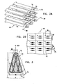
- Fig. 2A is a schematic illustration of an array 90 of electrode 64, in accordance with some applications of the present invention.
- Tip portions 70 of electrodes 64 are typically shaped to define a plurality of perforations passing therethrough.
- tips 70 are generally pointed, to facilitate tissue penetration.
- the perforated configuration of the tip allows for neuronal processes to intertwine with the electrode tips when electrodes 64 are disposed in retinal tissue of a subject. Increased and direct contact between the electrodes and the neuronal processes, improves the interaction between the neurons, e.g., bipolar cells, and the electrodes. Improved neuron/electrode interaction and coupling enhances stimulation of the neurons by the electrodes.
- Each tip 70 is typically shaped to define between 1 and 50 perforations (e.g., 1-10) passing therethrough.
- the perforations of each electrode are located 5-20 um (e.g., 10 um) from distal tip 72 and 10 - 30 um from tip-base 74.
- a spatial density of the perforations of each pointed tip is 0.001 - 0.02 perforations /um2, or 0.02 to 0.5 perforations /um2, e.g., 0.1 perforations /um2.
- each perforation has a diameter of 1 - 10 um.
- the diameter of the perforations in electrode 64 allows axons of bipolar cells, which typically have an average diameter of 1 um, to penetrate and grow through the perforations.
- electrodes 64 are disposed in the ganglion cell layer (GCL).
- GCL ganglion cell layer
- the axons of the ganglion cells grow through the perforations in electrode tips 70, increasing coupling between the neuronal processes and electrodes 64, and improving stimulation of the ganglion cell layer.
- the average diameter of the perforations is typically smaller than the average diameter of a retinal glial cell, which is typically larger than 10 um, preventing glial cells from passing through the perforations in the electrode. Preventing glial cells from passing through the perforations reduces glial encapsulation of the electrodes, and prolongs electrode function.
- the perforations are typically created by use of chemical treatments e.g., etching and/or a laser beam. For some applications, the same treatment is used to create the perforations and to increase surface roughness.
- a surface of tip 70 of electrode 64 is coated with carbon nanotubes, attracting neuronal processes to the perforations in tip 70 and increasing adhesion of the neuronal processes to the perforations.
- the carbon nanotube coating within the perforation can withstand penetration of neuronal processes into the perforations.
- Fig. 2B is a schematic illustration of an end view of array 90 of electrodes 64, in accordance with some applications of the present invention.
- Apparatus 60 typically comprises array 90 of electrodes 64 comprising at least 40 electrodes per mm2, e.g., between 100 and 400 electrodes per mm2.
- Fig 2B shows array 90 divided into nine units by way of illustration and not limitation. For some applications, each unit is 100 um x 100 um in size.
- Each unit typically comprises a pair of bipolar electrodes. For some applications, both bipolar electrodes (+ and -) in each unit protrude from array 90 and are configured to penetrate tissue of retina 6. One of these electrodes may be stimulating, and the other a return electrode, or else both may be stimulating.
- the stimulating electrode is longer than the return electrode in each pair, and reaches the bipolar layer, while the shorter return electrode only reaches the NFL layer.
- one electrode (either the + or the -) protrudes from array 90 and is configured to penetrate tissue of retina 6, and the other electrode, of opposite polarity, is a surface electrode that is not configured to penetrate tissue of retina 6, but rather functions as a return electrode.
- the distance D1 between the pair of bipolar electrodes 64 in each unit is typically between 5 and 50 um, e.g., 10 um.
- the distance D2 between electrodes of adjacent units is typically between 25 - 100 um, e.g., 50 um.
- the distance D1 between a pair of electrodes in each unit is smaller than (e.g., less than half of) the distance D2 between electrodes of adjacent units.
- Figs. 1 and 2A-B which is a Z view from the distal tip 72 of electrodes 64
- the major axis W1 of base portion 66 of insulated portion 68 is typically 1.5-2.5 (e.g., 2) times larger than the minor axis W2 of body portion 65.
- major axis W1 is 25 - 200 um, e.g., 50 - 150 um (e.g., 100 um)
- minor axis W2 is 10 - 100 um, e.g., 20 - 80 um (e.g., 50 um)
- electrodes 64 comprise bipolar electrodes that are configured to penetrate retinal tissue of a subject.
- Penetrating bipolar electrodes which are typically implanted such that both the stimulating and return electrodes are in close proximity to a neuronal retinal cell, require a smaller potential between the electrodes and enable reaching a higher potential drop across a given cell, resulting in enhanced stimulation of the cell. This is in contrast to many epi-retinal implants known in the art in which neuronal cells of the retina are stimulated by a surface electrode on the ILM layer.
- an array 90 of electrodes 64 is divided into clusters of electrodes.
- a cluster of three or more, e.g., 3 - 6, stimulating electrodes surround and share a common return electrode 8.
- Each electrode in the cluster receives a signal, through driving circuitry, from a discrete, respective, photosensor in support substrate 62, and in response, stimulates the retina of the subject.
- the return electrode typically has a sufficiently large surface area in order to accommodate the electric current returning from the cluster of stimulating electrodes.
- such an arrangement of array of electrodes 64 enables the use of a reduced number of electrodes, since several stimulating electrodes share a common return electrode.
- the stimulating electrodes are configured to drive currents into the cells of retina in alternating time periods. Such staggering of the driving of each electrode in the cluster reduces the amount of return electric current that is driven through the return electrode at a given time.
- array 90 comprises at least 10 clusters of electrodes, e.g., 50 - 150, or 100 - 500 clusters.
- array 90 may comprise 64 clusters, each cluster comprising 16 electrodes.
- array 90 comprises 500 - 1500 clusters of electrodes.
- Electrodes 64 are typically fabricated by conventional fabrication processes known in the art. For some applications, following fabrication, electrodes 64 are assembled on array 90 by methods such as "pick and place.” For other applications, other methods are used to fabricate array 90 of electrodes 64, e.g., three dimensional etching and/or MEMS Palladium etching technique. For some applications, techniques described in one or more of the following patents are practiced in combination with techniques and apparatus described herein: US Patent 7,096,568 , US Patent 6,678,458 , US Patent 6,923,669 , US Patent 6,473,365 , US Patent 6,762,116 US Patent 7,025,619 , US Patent 7,081,630 and US Patent 6,677,225 .
- Apparatus 60 comprises electrodes which, for some applications, are shaped to define respective pointed tips configured for penetrating tissue of the subject.
- Each tip 70 is typically an electrically exposed tip, configured to directly drive current into the retinal tissue, e.g., bipolar cell layer, causing stimulation of the tissue and resulting in enhanced vision.
- Exposed tip 70 of the electrode typically has a length L2 of between 25 um and 100 um, e.g., 50 um.
- each tip 70 is pointed when viewed from a distance, and thus functions as a pointed tip for purposes such as penetrating tissue, a close examination of the tip 70 reveals that it is shaped to have a radius of curvature R of 0.5 - 10 um, e.g., 2 um.
- Tip 70 may be shaped to define a tip having an angle alpha of 30 - 60 degrees. As shown in Fig. 3 , tip 70 comprises a tip-base portion 74 and a distal tip 72. Base portion 74 of tip 70, which is at a distal end of the electrode body portion, has a width W5 of between 15 um and 60 um, e.g., 30 um. Tip 70 typically decreases monotonically in width along its longitudinal axis from tip-base portion 74 to distal tip 72, until it reaches a width W6 of between 1 um and 20 um, e.g., 10 um, 4 um proximal from distal tip-end 72. For some applications, tip 70 is reduced in size after electrode shaping by techniques such as laser ablation.
- tip 70 typically decreases monotonically in thickness along its longitudinal axis from base portion 74 to distal tip 72.
- Base portion 74 of tip 70 has a thickness T1 of between 5 um and 20 um, e.g., 10 um.
- Distal tip 72 of tip 70 has a thickness T2 of between 0.5 um and 5 um, e.g., 2 um.
- the shape of the distal tip of tip 70, and a radius of curvature R of tip 70 typically reduces the extent to which tip 70 penetrates and/or ruptures cells with which it comes in contact.
- retinal neuronal cells range between 5 and 10 um.
- Radius of curvature R is typically 0.5 um - 10 um, e.g., 2 um, roughly in the same magnitude as the cells.
- all edges of electrode tip 70 and electrode 64 have a radius of curvature that is greater than 0.1 um, e.g., greater than 0.5 um. Rounding of the edges is typically done to reduce concentration of charge at sharp edges. Surface treatments to increase roughness of a surface of tip 70, as described hereinbelow, are also used to smoothen and round edges of tip 70 and electrode 64.
- tip 70 of electrode 64 is treated to increase surface roughness of tip 70.
- an area 73 of tip 70 is treated to increase roughness, whereas another area 75 of tip 70 remains untreated in order to maintain structural strength of the tip.
- Figs. 2A-B and 3 As shown in Fig. 3 , untreated areas 75 are maintained in order to strengthen tip 70 for withstanding compression forces applied during penetration of tip 70 into retinal tissue.
- Surface treatment of the tip in areas 73 typically affects an area of the tip that is as deep as 2 um from the surface. Increased surface roughness causes an increased surface area of the tip.
- the tip is treated to increase roughness such that 1 mm2 area has an equivalent surface area of between 10 mm2 and 1000 mm2, e.g., 100 mm2.
- Increased surface area generally reduces electrode impendence, thereby enhancing stimulation of retinal tissue by electrodes 64.
- increased roughness generally reduces surface charge density and improves electrode capacitance, enabling an increase in the charge injection limit.
- Increased surface roughness to reduce charge density is typically achieved by techniques of nanofabrication and/or metal etching, as described in Liang et al., in an article entitled “Surface modification of cp-Ti using femtosecond laser micromachining and the deposition of Ca/P layer” Materials Letters Volume 62, Issue 23, 31 August 2008, Pages 3783-3786 .
- electrodes 64 are coated with carbon nanotubes.
- carbon nanotubes create a rough surface in electrode 64, including tip portion 70.
- Rough surfaces in general and carbon nanotube surfaces in particular have been shown to attract neurons and promote neuronal growth.
- neurons were found to bind and preferentially anchor to carbon nanotube rough surfaces.
- adhesion of retinal neurons e.g., bipolar cells
- carbon nanotube electrodes provided by these applications of the present invention, promotes cell-electrode coupling and/or axon regeneration, leading to improved stimulation of the retina.
- the carbon nanotube coating of electrode 64 is glued to the electrode surface and/or grown on a selected surface of the electrode by using doping techniques known in the art.
- a femtosecond laser is used to increase surface roughness of electrodes 64.
- Femtosecond laser treatment produces rough surface structures on titanium possibly for the use of implants and other biomedical applications treatments (Vorobyev et al., 2007).
- femtosecond laser treatment increases the roughness of a titanium substrate in the range of 1-15 um.
- femtosecond laser treatment was shown to produce a variety of surface nanostructures, such as nanoprotrusions and nanopores on the titanium substrate. Liang et al., cited above, report good bioactivity of a pure titanium substrate that was treated with a femtosecond laser to increase roughness of its surface.
- a blanket etch MEMS procedure is used to increase surface roughness of electrodes 64.
- the entire electrode 64 is blanketed and tip 70 is etched to increase surface roughness and achieve a desired aspect ratio in a similar procedure to that described in US 6,770,521 to Visokay .
- Apparatus 60 typically comprises an array 1090 of protruding electrodes 1064 configured to penetrate the retina of a subject. It is to be noted that techniques and apparatus described hereinabove with reference to electrodes 64 and array 90 apply to electrodes 1064 and array 1090, except where otherwise indicated. For some applications, electrodes 1064 vary in length. Electrodes 61 are generally longer than electrodes 62, thereby facilitating direct stimulation of distinct areas of the retina, e.g., the bipolar layer and/or the ganglion cell layer. Other dimensions of the electrodes are described hereinbelow, with reference to Fig. 6 .
- Electrodes 1064 comprise any suitable material e.g., palladium and/or titanium, and/or silicon electrodes.
- electrodes 1064 comprise a metal alloy and/or doped electrodes.
- a silicon wafer 1030 forms the base of array 1090 from which electrodes 1064 protrude.
- wafer 1030 is selectively etched to a desired depth by using any suitable technique known in the art, e.g., techniques of Deep Reactive Ion Etching (DRIE).
- DRIE Deep Reactive Ion Etching
- electrodes 1064 are etched by using any suitable technique known in the art, e.g., techniques of Deep Reactive Ion Etching (DRIE), to have desired dimensions and aspect ratios.
- DRIE Deep Reactive Ion Etching
- additional metals such as platinum, and/or palladium, are deposited on electrodes 1064 by using, for example, a shadow mask technique.
- An attaching titanium ring frame 1020 is typically electroplated with electrodes 1064 to form a structure that can subsequently be welded to the metal ring case 2020 (shown in Fig. 5 ).
- the silicon wafer 1030 is typically biocompatible.
- Ring frame 1020 is typically bonded to silicon wafer 1030, by using, e.g., fusion bonding. Suitable fusion bonding techniques are described in an article by Jourdain et al., entitled, "Fabrication of piezoelectric thick-film bimorph micro-actuators from bulk ceramics using batch-scale methods," which is incorporated herein by reference.
- Wafer 1030 typically comprises through-wafer vias.
- apparatus 60 additionally comprises a CMOS chip 1040 including through-silicon vias.
- CMOS chip 1040 including through-silicon vias.
- solder bumps 1050 are deposited on an upper side of CMOS chip 1040, electrically connecting chip 1040 to silicon wafer 1030.
- apparatus 60 comprises a layer 1060.
- Layer 1060 typically comprises additional elements of an intraocular retinal prosthesis, e.g., an energy receiving layer, a photosensor layer and driving circuitry that is powered by the energy receiving layer.
- the driving circuitry typically drives current into the retinal tissue from the rough tips 1070 of electrodes 1064, in response to sensing by the photosensor layer, in order to stimulate the retinal tissue.
- the electrical signal generated by layer 1060 is typically routed through silicon wafer 1030 to electrodes 1064, providing sealing on one side and electrical contact on the other.
- a back side of the titanium wafer is bound to a glass cap 80 which, as shown in Fig. 4B , encapsulates the entirety of apparatus 60, excluding array 1090 of protruding electrodes 1064.
- glass cap 80 comprises two distinct glass pieces, one of which is shaped to define a hole. The glass pieces are typically bonded to each other by anodic bonding, forming a single glass cap 80. Bonding of titanium frame 1020 to glass cap 80 is optionally done using thermal compression bonding. This low temperature bonding step generally does not affect circuitry of apparatus 60. Glass cap 80 generally reduces exposure of human tissue to any toxic materials, e.g., contaminated silicon, which may exist in apparatus 60. Typically, laser welding is used to close the glass encapsulation.
- apparatus 60 typically comprises array 1090 of electrodes 1064, which are configured to penetrate retinal tissue of a subject.
- electrodes 1064 comprise long electrodes 61 and short electrodes 62.
- Array 1090 is typically bonded to silicon wafer 1030 which is coupled to CMOS chip 1040 via solder bumps 1050.
- apparatus 60 comprises a metal ring 2020 which encapsulates the entirety of apparatus 60, excluding array 1090 of protruding electrodes 1064.
- each electrode in apparatus 60 comprises an electrically-insulated body portion coupled to an electrically exposed distal tip.
- Fig. 5 shows an exploded view of electrodes 1064 showing body portion 1068 of electrodes 1064 coated with a polyimide insulating coating 82.
- Tip 1070 of electrode 1064 remains electrically exposed, i.e., not coated with a polyimide coating, to enable an electrical connection between the tip and the bipolar layer (or other portions of the retina).
- tip 1070 physically contacts the bipolar layer when apparatus 60 is implanted in the eye of a subject.
- the entire electrode is fabricated to include a polyimide coating, followed by for example, an etching process to selectively remove the polyimide coating from electrode tip 1070.
- the polyimide coating is removed from the tip 70 by laser ablation.
- Fig. 5 shows tip 1070 having a rough surface to increase neuronal cell adhesion to tip 1070, thus increasing tissue stimulation by electrodes 1064.
- tip 1070 is configured to penetrate retinal tissue of a subject.
- apparatus 60 is configured to match the natural curvature of the retina to facilitate implantation and anchoring of apparatus 60 to the retina.
- electrodes 1064 typically vary in length, and as indicated by Figs. 4A-B and 5 , for some applications, tips 1070 of electrodes 1064 together define a convex curved surface having a radius of curvature that is 6 - 15 mm.
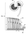
- FIG. 6 is a schematic illustration of a section of array 1090 of electrodes 1064, in accordance with some applications of the present invention.
- array 1090 typically comprises electrodes 1064 of varying heights.
- electrodes 1064 are arranged in concentric circles on wafer 1030.
- the circles of electrodes 1064 typically alternate between long electrodes 61 and short electrodes 62, such that electrodes 1064 are typically arranged in pairs of bipolar electrodes.
- Each pair of electrodes typically comprises a single long electrode 61 and a single short electrode 62.
- Apparatus 60 and electrodes 1064 are typically configured to match the natural curvature of a human organ and/or tissue in which it is implanted, e.g., the retina. As shown in Fig. 6 , for some applications, electrodes 1064 vary in length. Electrodes 61 are generally longer than the electrodes 62, thereby facilitating direct stimulation of distinct areas of the retina, e.g., the bipolar layer and/or the ganglion cell layer. For some applications, long electrodes 61 have a length L3 of 200 - 800 um, e.g., 300-500. Short electrodes 62 typically have a length L4 of 100 - 550 um, e.g., 150-350.
- long electrodes 61 are 50 - 150 um longer than the adjacent short electrodes 62.
- both long electrodes 61 and short electrodes 62 function as stimulating electrodes.
- long electrodes 61 function as stimulating electrodes and short electrodes 62 function as return electrodes.
- return electrodes 62 are less than 10 um in length, and may even comprise surface electrodes. In this case, L4 is less than 5 um in length.
- FIG. 7 is a schematic illustration of apparatus 60 disposed in retina 6, in accordance with some applications of the present invention.
- Fig. 7 shows components of apparatus 60 (silicon wafer 1030, attaching ring frame 1020, CMOS chip 1040, solder bumps 1050 and layer 1060) in glass encapsulation 80. Electrodes 1064 are shown penetrating retina 6. For some applications, and as described hereinabove with reference to Fig. 6 , electrodes 1064 of apparatus 60 are arranged in pairs of bipolar electrodes. For some applications, both bipolar electrodes (+ and -) of each pair protrude from apparatus 60, and are configured to penetrate tissue of retina 6.
- the electrodes in each pair are of varying lengths, such that one electrode (either the + or the -) is longer than the second electrode.
- the longer electrode 61 e.g., 200 - 800 um in length
- the shorter electrode 62 e.g., 100 - 550 um in length
- the longer electrode 61 is configured to protrude from apparatus 60 and penetrate retinal tissue in order to contact and stimulate the bipolar cell layer.
- the shorter electrode 62 e.g., 100 - 550 um in length
- short electrode 62 is configured to penetrate and stimulate retinal ganglion cells.
- long electrodes 61 function as stimulating electrodes, e.g., to stimulate the bipolar layer and short electrodes 62 function as return electrodes.
- one electrode protrudes from apparatus 60 and is configured to penetrate tissue of retina 6, and the other electrode, of opposite polarity, is a surface electrode that is not configured to penetrate tissue of retina 6, but rather functions as a return electrode (application not shown).
- apparatus 60 comprises at least 100 short or surface electrodes, and at least 400 long electrodes.
- electrodes 1064 comprise hook electrodes configured to anchor to retinal tissue of a subject, increasing coupling between the target cells and the electrode.
- apparatus 60 including substrate 62, is flexible and can be adjusted to match the natural curvature of the retina during implantation.
- Apparatus 60 may be adjusted to match the retina of a subject by standard fitting and/or can be tailor made according to OCT imaging of the retina. Once adjusted to match the natural curvature of the retina, apparatus 60 is typically glued and/or stitched in place.
- apparatus 60 is generally rigid, and electrodes of varying heights and, optionally, shapes enable proper attachment of the apparatus to the curved structure of the retina.
- a plurality of implantable apparatuses 60 may be implanted in discrete locations in tissue of retina 6, either arranged in an array, or, for example, pseudo-randomly.
- apparatus 60 is wireless and does not comprise bulky components, facilitating implantation of several implants 60 in retina 6 of the subject.
- a system comprising penetrating electrodes with rough and/or perforated tips as described hereinabove with reference to Figs. 1-7 , may be implanted in any other organ (e.g., brain, nose, ears and/or tongue), and used in any other neurological application (e.g., cortex stimulation).
- Implantation of penetrating electrodes as described hereinabove in, for example, brain tissue of a subject typically reduces the amount of power required to stimulate the tissue. Additionally or alternatively, implantation of such electrodes facilitates specific sensing and enhances specific stimulation of a target neuron in the tissue by directly contacting selective areas with the electrodes.
- a system comprising penetrating electrodes as described hereinabove may be used to stimulate organs such as the liver or the pancreas. Implanting an array of such electrodes in, for example, selected areas of pancreatic tissue (e.g., insulin-secreting areas) enables specific and more effective stimulation of these areas.
Landscapes
- Health & Medical Sciences (AREA)
- Life Sciences & Earth Sciences (AREA)
- Public Health (AREA)
- Heart & Thoracic Surgery (AREA)
- Engineering & Computer Science (AREA)
- Biomedical Technology (AREA)
- Nuclear Medicine, Radiotherapy & Molecular Imaging (AREA)
- Cardiology (AREA)
- Animal Behavior & Ethology (AREA)
- Radiology & Medical Imaging (AREA)
- General Health & Medical Sciences (AREA)
- Ophthalmology & Optometry (AREA)
- Veterinary Medicine (AREA)
- Electrotherapy Devices (AREA)
- Prostheses (AREA)
- Materials For Medical Uses (AREA)
Description
- Some applications of the invention relate generally to implantable medical devices and more specifically to a retinal electrode assembly.
- Retinal malfunction, due to degenerative retinal diseases, is a leading cause of blindness and visual impairment. Implantation of a retinal prosthesis is a technology for restoring some useful vision in individuals suffering from retinal-related blindness.
- The retina is a multi-layered light-sensitive structure that lines the posterior, inner part of the eye. The retina contains photoreceptor cells, for example rods and cones, which capture light and convert light signals into neural signals transmitted through the optic nerve to the brain. A bipolar cell layer exists between the photoreceptors and ganglion cells of the retina. The bipolar cell layer transmits signals from the photoreceptors to the ganglion cells whose axons form the optic nerve and transmit visual information to the brain.
-
US-A-4 628 933 discloses a visual prosthesis according to the pre-characterizing portion ofclaim 1. -
US-A-4 969 468 discloses an electrode array for establishing electrical contact with tissue of a living body. -
US-B1-7127 301 discloses a micro-machined electrode array for interfacing with neural tissue for use in an implantable retinal prosthesis. -
US-A1-2009/005835 discloses an implantable device for a visual prosthesis. -
US-A1-2004/088026 discloses an artificial retina device comprising a plurality of multi-phasic microphotodiode subunits. - In accordance with the present invention, there is provided an apparatus configured for implantation in a body of a subject, as defined in appended
claim 1. Embodiments of the invention are defined in the appended claims which are dependent onclaim 1. - In some applications of the present invention, implantable intraocular apparatus is provided for stimulating a retina of a subject suffering from a retinal disease and restoring at least partial vision in the subject
- The intraocular apparatus, which is implanted entirely in the subject's eye, typically comprises an intraocular retinal prosthesis, configured to be implanted in the subject's eye in either an epi-retinal or a sub-retinal position.
- The apparatus typically comprises a support substrate and an array of electrodes protruding from the support substrate. (In this context, in the specification and in the claims, "array" is meant to include rectangular as well as non-rectangular arrays (such as circular arrays). The protruding electrodes are shaped to define electrically-exposed tips which penetrate retinal tissue of the subject, bringing the electrodes in contact with the tissue. For some applications, a surface of the electrodes is treated to increase roughness and surface area of the electrodes, thus reducing electrode impendence and facilitating retinal stimulation and/or axon regeneration. Additionally or alternatively, the exposed tips of the electrodes have perforations passing therethrough, further increasing the surface area of the electrodes and allowing neuronal processes, to pass through and intertwine with the electrodes.
- For some applications, the support substrate from which the electrodes protrude comprises additional elements of a retinal prosthesis, e.g., an energy receiving layer, a photosensor layer and driving circuitry that is powered by the energy receiving layer. The driving circuitry typically drives current into the retinal tissue from the perforated rough tips of the electrodes, in response to sensing by the photosensor layer, in order to stimulate the retinal tissue.
- The inventors have identified that, for some applications, sufficient stimulation of retinal tissue is a characteristic for consideration in enabling proper function of a retinal prosthesis. In particular, facilitating stimulation of the bipolar cell layer of the retina, which in turn stimulates ganglion cells, is a characteristic for consideration in retinal prosthesis provided by some applications of the present invention. The ganglion cells, whose axons form the optic nerve, further transmit the visual information to the brain resulting in the formation of an image. Penetrating perforated electrodes, in contrast to surface electrodes known in the art which sit on the surface of tissue, are configured to extend from either an epi-retinal or a sub-retinal implantation site and penetrate retinal tissue to directly contact and drive current into the bipolar cell layer from typically less than 10 um from the nearest bipolar cell. Rough electrode surfaces and perforations passing through the electrodes allow neuronal processes to grow therethrough, further improving cell-electrode coupling and increasing stimulation. Increased and direct contact of the retinal tissue by penetrating perforated electrodes enhances stimulation of the retina resulting in enhanced image resolution.
- There is therefore provided in accordance with the present invention an apparatus configured for implantation in a body of a subject, comprising: a support substrate; and electrodes protruding from the support substrate, each electrode having a distal tip; characterized in that at least 500 of the electrodes protrude at least 50 um from the support substrate, with each electrode further having (a) an electrically-exposed tip portion, (b) an electrically-insulated body portion, proximal to the electrically-exposed tip portion, and (c) a cross-section of 50-1500 um2, 20 um from the distal tip, and with the distal tip of each electrode having a radius of curvature of 0.5 - 5 um.
- For some applications, each electrode has a cross section of at least 200 um2, 20 um from the distal tip.
- For some applications, the at least 500 electrodes include 1000-3000 electrodes.
- For some applications, the at least 500 electrodes include 3000-6000 electrodes.
- For some applications, a spatial density of the electrodes is 50 - 400 electrodes per mm2.
- For some applications, the electrodes protrude perpendicularly from the support substrate.
- For some applications, each electrode tip has a rough surface.
- For some applications, the rough surface has a surface area that is increased by a factor of more than 50 due to being rough.
- For some applications, some area of the tips of the electrodes is coated with carbon nanotubes.
- For some applications, the apparatus is configured for implantation in an eye of the subject.
- For some applications, the eye of the subject includes retinal tissue of the subject, and the tips are configured to penetrate the retinal tissue.
- For some applications, the retinal tissue of the subject includes a retinal bipolar cell layer of the subject, and the tips are configured to penetrate the retinal bipolar cell layer.
- For some applications, the tissue of the subject includes a retinal ganglion cell layer of the subject, and the tips are configured to penetrate the retinal ganglion cell layer.
- For some applications, the electrodes include silicon.
- For some applications, the electrodes include titanium.
- For some applications, the electrodes include palladium.
- For some applications, the electrically-exposed tip portion of each electrode is 25 - 100 um in length.
- For some applications, the electrically-insulated body portion has a length of 75-200 um.
- For some applications, the electrically-insulated body portion has a length of 200 - 700 um.
- For some applications, the electrically-insulated body portion has a length of 100 - 650 um.
- For some applications, the electrically-insulated body portion includes an elliptical base portion at a proximal end of the body portion.
- For some applications, the elliptical base portion has a major axis of 50 - 150 um and a minor axis of 25 - 80 um, the major axis being at least two times longer than the minor axis.
- For some applications, the electrically-exposed tip portion of each electrode has an area of at least 750 um2.
- For some applications, a cross-sectional area of each electrode declines monotonically from (a) a point 50 um from the distal tip to (b) the distal tip.
- For some applications, the electrically-exposed tip portion of each electrode has a width of 15 - 60 um at a point 50 um from the distal tip.
- For some applications, the electrically-exposed tip portion of each electrode has a width of 1- 20 um at a point 4 um from the distal tip.
- For some applications, the electrically-exposed tip portion of each electrode has a thickness of 5 - 20 um at a point 50 um from the distal tip.
- For some applications, the electrically-exposed tip portion of each electrode has a thickness of 0.5 - 5 um at a point 4 um from the distal tip.
- For some applications, the radius of curvature of the distal tips is 1 - 3 um.
- For some applications, a distance from the substrate to the distal tip of each electrode is 200 - 500 um.
- For some applications, the distal tip of the tips of the electrodes have an average distance from the support substrate of 20-150 um.
- For some applications, the support substrate includes an energy receiving layer and a photosensor layer, and the apparatus further includes driving circuitry that is powered by the energy receiving layer and drives current into the tissue from the tips of the electrodes, in response to sensing by the photosensor layer.
- For some applications, the electrically-exposed tip portion of each electrode is shaped to define a book configured to penetrate the tissue of the subject and anchor to the tissue.
- For some applications, the support substrate is generally flexible.
- For some applications, the flexible support substrate is bendable during implantation of the apparatus in order to match a natural curvature of a retina of the subject.
- For some applications, the tips of the electrodes together define a convex curved surface having a radius of curvature that is 6 - 15 mm.
- For some applications, the apparatus includes at least 100 surface electrodes, and the protruding electrodes are shaped to define respective tips having rough surfaces and configured for penetrating tissue of the subject.
- For some applications, the surface electrodes are configured to function as return electrodes.
- For some applications, the at least 500 electrodes are arranged in at least 10 clusters of three or more electrodes, the distal tips being configured for penetrating tissue of the subject, and:
- at least some of the electrodes in each cluster are configured to drive respective currents into the tissue of the subject, and
- the current driven by each electrode in the cluster is returned via an electrode in the cluster that serves as a common return electrode for the other electrodes in the cluster.
- For some applications, at least some of the clusters include fewer than six electrodes.
- For some applications, at least some of the clusters include 10 - 50 electrodes.
- For some applications, at least some of the clusters include 16 electrodes.
- For some applications, the at least 10 clusters include 50 - 150 clusters.
- For some applications, the at least 10 clusters include 64 clusters.
- For some applications, the at least 10 clusters include 100-500 clusters.
- For some applications, the at least 10 clusters include 500-1500 clusters.
- For some applications, the electrically-exposed tip portion of each electrode is shaped to define one or more perforations passing therethrough and is configured for penetrating tissue of the subject.
- The present invention will be more fully understood from the following detailed description of applications thereof, taken together with the drawings, in which:
-
-
Fig. 1 shows a system for restoring at least partial vision in a subject in accordance with some applications of the present invention; -
Figs. 2A-B are schematic illustrations of an array of penetrating electrodes, in accordance with some applications of the present invention; -
Fig. 3 is a schematic cross-sectional illustration of a pointed tip an of electrode, in accordance with some applications of the present invention; -
Figs. 4A-B are schematic illustrations of apparatus for retinal stimulation, in accordance with some applications of the present invention; -
Fig. 5 is a schematic illustration of apparatus for retinal stimulation, in accordance with some applications of the present invention; -
Fig. 6 is a schematic illustration of an array of penetrating electrodes, in accordance with some applications of the present invention; and -
Fig. 7 is a schematic illustration of intraocular apparatus penetrating retinal tissue, in accordance with some applications of the present invention. -
Fig. 1 shows asystem 20 for restoring at least partial vision in a subject, a portion of which is implanted in an eye of the subject, in accordance with some applications of the present invention. - Vision is initiated when light reflecting from objects is focused by lens 2 of eye 4 onto the
retina 6.Fig. 1 shows a cross section of a portion of a human retina. The retina is approximately 0.2-0.5 mm thick and lines the back of the eye. As shown, the retina consists of three layers of neurons:photoreceptor cells 10,ganglion cells 12 andmany intemeurons 15 packed into the central part of the section of the retina intervening between the photoreceptors and the ganglion cells. The ganglion cells, which transmit visual information to the brain, lie innermost (as used herein) in the retina, i.e., on the side of the retina closest to the lens and front of the eye. The photoreceptor cells (e.g., rods and cones), which capture light and convert light signals into neural signals, lie outermost in the retina. The central part of the section of retina located between the photoreceptors and the ganglion cells includes the inner nuclear layer (INL), which is made up ofbipolar cells 14 and other cells. - The bipolar cell layer typically transmits signals from the
photoreceptors 10 to theganglion cells 12. The rod and cone photoreceptors transfer a signal to the bipolar cells that lay adjacent to the photoreceptor layer. The bipolar cell layer then transmits the signal to the ganglion cells whose axons form the optic nerve. Thebipolar cell layer 14 is generally located in a region of the retina that is approximately 130 um - 200 um from the inner limiting membrane (ILM), which is the boundary between the vitreous humor in the posterior chamber and the retina itself. - As shown in
Fig. 1 , for some applications,intraocular apparatus 60 is implanted in an epi-retinal position, typically coupled to the ILM. As described in Zrenner, 2002, epi-retinal arrays are typically implanted onto the retinal surface that separates the retinal neural layer from the vitreous body of the eye's posterior chamber, such that the implant is typically located outside of the vitreous body, contacting the ILM. As appropriate, techniques described in one or more of these references may be adapted for use in implantingapparatus 60. - For some applications,
apparatus 60 is implanted in a sub-retinal position (not shown). As described in Zrenner, 2002, sub-retinal arrays are typically implanted between the pigmentepithelial layer 30 and the layer of the retina which contains the photoreceptor cells. - As provided by some applications of the present invention,
apparatus 60 comprises asupport substrate 62 and a plurality ofelectrodes 64 protruding from the support substrate. For some applications supportsubstrate 62 comprises components of an intraocular retinal prosthesis. For example,support substrate 62 may comprise an energy receiving layer, a photosensor layer and driving circuitry. The driving circuitry is powered by the energy receiving layer, which typically receives energy from an external device comprising an external power source 24 (e.g., a laser coupled to the frame of a pair ofeyeglasses 25, and/or an RF energy source, and/or a magnetic energy source). For some applications a partially-transparent (e.g., half-silvered) mirror 23 is coupled toeyeglasses 25, providing ophthalmoscope functionality to the external device. It is to be noted that for some applications, techniques and apparatus described inUS Patent Application 12/368,150 to GrossUS2010-0204754 , with reference to the external device including the partially transparent mirror, are combined with techniques and apparatus described herein. - The driving circuitry drives
electrodes 64 to apply currents to the retina, in response to sensing by the photosensor layer, in order to stimulate theretina 6. Accordingly,system 20 for restoring vision in a subject does not comprise an extraocular camera, andapparatus 60 does not receive image data from outside the eye, but rather utilizes the intact optics and processing mechanisms of the eye 4. -
Apparatus 60 typically comprises approximately 500-6000, e.g., 1000-4000, typically 1600electrodes 64. For some applications, the electrodes protrude perpendicularly at least 50 um from the support substrate. - Each electrode is typically 100-1000 um in length e.g., 300-600 um, for example, 400 um, in order to reach the outer plexiform layer (OPL), where connections between the bipolar cell layer and the adjacent photoreceptor layer occur. For some applications, each electrode comprises an electrically-insulated
body portion 68 coupled to an electrically exposedtip portion 70.Insulated portion 68 of the electrode has a length L1 of between 100 um and 650 um, e.g., 150 um.Exposed tip 70 ofelectrode 64 typically has a length L2 of between 25 um and 100 um, e.g., 50 um. Typically,electrode 64 has an exposed area of 750 um2. Theelectrodes 64 protrude fromsupport substrate 62, such that whenapparatus 60 is implanted in an eye of a subject,electrodes 64 penetrate tissue ofretina 6 and exposedtip portions 70 are typically disposed inbipolar layer 14. Other dimensions of the electrodes are described hereinbelow, with reference toFigs. 2 - 3 . -
Fig. 1 shows a schematic illustration ofelectrode 64, in accordance with some applications of the present invention. As shown, theinsulated portion 68 ofelectrode 64 includes an ellipticalproximal base portion 66 and anelongated body portion 65 extending between the base portion and the exposedtip 70.Tip 70 typically comprisesdistal tip 72 andtip base 74.Base portion 66 typically has a major axis W1 of between 25 um and 200 um, e.g., 100 um, and a minor axis W2 that is typically 10 - 100 um, e.g., 50 um.Base portion 66 typically has a larger average diameter thanbody portion 65, contributing to the structural strength ofelectrode 64.Body portion 65 is typically generally elliptical, and has a major axis W3 of between 15 um and 60 um, e.g., 30 um, and a minor axis W4 between 5 um and 20 um, e.g., 10 um. Typically,electrodes 64 have a cross-section of 50 - 200 um2, 20 um fromdistal tip 72. For someapplications electrodes 64 have a cross-section of at least 200 um2, 20 um fromdistal tip 72. - For some applications, each
electrode 64 is typically 25-100 um in length e.g., 50 um, in order to penetrate the nerve fiber layer (NFL) and reach the ganglion cell layer (GCL) 12. Contacting the ganglion cells byelectrodes 64 typically enables the use of a reduced amount of power in order to stimulate the ganglion cells. Close proximity toganglion cells 12 generally results in more focused stimulation that enables higher pixel density for a given amount of current. - Reference is made to
Fig. 2A , which is a schematic illustration of anarray 90 ofelectrode 64, in accordance with some applications of the present invention.Tip portions 70 ofelectrodes 64 are typically shaped to define a plurality of perforations passing therethrough. In some applications,tips 70 are generally pointed, to facilitate tissue penetration. The perforated configuration of the tip allows for neuronal processes to intertwine with the electrode tips whenelectrodes 64 are disposed in retinal tissue of a subject. Increased and direct contact between the electrodes and the neuronal processes, improves the interaction between the neurons, e.g., bipolar cells, and the electrodes. Improved neuron/electrode interaction and coupling enhances stimulation of the neurons by the electrodes. Eachtip 70 is typically shaped to define between 1 and 50 perforations (e.g., 1-10) passing therethrough. For some applications, the perforations of each electrode are located 5-20 um (e.g., 10 um) fromdistal tip 72 and 10 - 30 um from tip-base 74. - Typically, a spatial density of the perforations of each pointed tip is 0.001 - 0.02 perforations /um2, or 0.02 to 0.5 perforations /um2, e.g., 0.1 perforations /um2. For some applications, each perforation has a diameter of 1 - 10 um. The diameter of the perforations in
electrode 64 allows axons of bipolar cells, which typically have an average diameter of 1 um, to penetrate and grow through the perforations. - As mentioned hereinabove, for some
applications electrodes 64 are disposed in the ganglion cell layer (GCL). In such applications, the axons of the ganglion cells grow through the perforations inelectrode tips 70, increasing coupling between the neuronal processes andelectrodes 64, and improving stimulation of the ganglion cell layer. - The average diameter of the perforations is typically smaller than the average diameter of a retinal glial cell, which is typically larger than 10 um, preventing glial cells from passing through the perforations in the electrode. Preventing glial cells from passing through the perforations reduces glial encapsulation of the electrodes, and prolongs electrode function.
- The perforations are typically created by use of chemical treatments e.g., etching and/or a laser beam. For some applications, the same treatment is used to create the perforations and to increase surface roughness. For some applications, a surface of
tip 70 ofelectrode 64 is coated with carbon nanotubes, attracting neuronal processes to the perforations intip 70 and increasing adhesion of the neuronal processes to the perforations. Typically, the carbon nanotube coating within the perforation can withstand penetration of neuronal processes into the perforations. - Reference is made to
Fig. 2B , which is a schematic illustration of an end view ofarray 90 ofelectrodes 64, in accordance with some applications of the present invention.Apparatus 60 typically comprisesarray 90 ofelectrodes 64 comprising at least 40 electrodes per mm2, e.g., between 100 and 400 electrodes per mm2.Fig 2B showsarray 90 divided into nine units by way of illustration and not limitation. For some applications, each unit is 100 um x 100 um in size. Each unit typically comprises a pair of bipolar electrodes. For some applications, both bipolar electrodes (+ and -) in each unit protrude fromarray 90 and are configured to penetrate tissue ofretina 6. One of these electrodes may be stimulating, and the other a return electrode, or else both may be stimulating. For some applications, the stimulating electrode is longer than the return electrode in each pair, and reaches the bipolar layer, while the shorter return electrode only reaches the NFL layer. For other applications, one electrode (either the + or the -) protrudes fromarray 90 and is configured to penetrate tissue ofretina 6, and the other electrode, of opposite polarity, is a surface electrode that is not configured to penetrate tissue ofretina 6, but rather functions as a return electrode. The distance D1 between the pair ofbipolar electrodes 64 in each unit is typically between 5 and 50 um, e.g., 10 um. The distance D2 between electrodes of adjacent units is typically between 25 - 100 um, e.g., 50 um. Generally, the distance D1 between a pair of electrodes in each unit is smaller than (e.g., less than half of) the distance D2 between electrodes of adjacent units. - Reference is made to
Figs. 1 and2A-B . As shown inFig. 2B , which is a Z view from thedistal tip 72 ofelectrodes 64, the major axis W1 ofbase portion 66 ofinsulated portion 68 is typically 1.5-2.5 (e.g., 2) times larger than the minor axis W2 ofbody portion 65. Typically, major axis W1 is 25 - 200 um, e.g., 50 - 150 um (e.g., 100 um), and minor axis W2 is 10 - 100 um, e.g., 20 - 80 um (e.g., 50 um) - Reference is again made to
Figs. 1 and2A-B . As mentioned hereinabove, for some applications,electrodes 64 comprise bipolar electrodes that are configured to penetrate retinal tissue of a subject. Penetrating bipolar electrodes, which are typically implanted such that both the stimulating and return electrodes are in close proximity to a neuronal retinal cell, require a smaller potential between the electrodes and enable reaching a higher potential drop across a given cell, resulting in enhanced stimulation of the cell. This is in contrast to many epi-retinal implants known in the art in which neuronal cells of the retina are stimulated by a surface electrode on the ILM layer. - For some applications, an
array 90 ofelectrodes 64 is divided into clusters of electrodes. For such applications, a cluster of three or more, e.g., 3 - 6, stimulating electrodes, by way of illustration and not limitation, surround and share a common return electrode 8. Each electrode in the cluster receives a signal, through driving circuitry, from a discrete, respective, photosensor insupport substrate 62, and in response, stimulates the retina of the subject. In such applications, the return electrode typically has a sufficiently large surface area in order to accommodate the electric current returning from the cluster of stimulating electrodes. Generally, such an arrangement of array ofelectrodes 64 enables the use of a reduced number of electrodes, since several stimulating electrodes share a common return electrode. For some applications, the stimulating electrodes are configured to drive currents into the cells of retina in alternating time periods. Such staggering of the driving of each electrode in the cluster reduces the amount of return electric current that is driven through the return electrode at a given time. For some applications,array 90 comprises at least 10 clusters of electrodes, e.g., 50 - 150, or 100 - 500 clusters. For example,array 90 may comprise 64 clusters, each cluster comprising 16 electrodes. For some applications,array 90 comprises 500 - 1500 clusters of electrodes. - Reference is again made to
Figs. 2A-B .Electrodes 64 are typically fabricated by conventional fabrication processes known in the art. For some applications, following fabrication,electrodes 64 are assembled onarray 90 by methods such as "pick and place." For other applications, other methods are used to fabricatearray 90 ofelectrodes 64, e.g., three dimensional etching and/or MEMS Palladium etching technique. For some applications, techniques described in one or more of the following patents are practiced in combination with techniques and apparatus described herein:US Patent 7,096,568 ,US Patent 6,678,458 ,US Patent 6,923,669 ,US Patent 6,473,365 ,US Patent 6,762,116 US Patent 7,025,619 ,US Patent 7,081,630 andUS Patent 6,677,225 . - Reference is now made to
Fig. 3 , which is a schematic cross-sectional illustration of atip portion 70, in accordance with some applications of the present invention.Apparatus 60 comprises electrodes which, for some applications, are shaped to define respective pointed tips configured for penetrating tissue of the subject. Eachtip 70 is typically an electrically exposed tip, configured to directly drive current into the retinal tissue, e.g., bipolar cell layer, causing stimulation of the tissue and resulting in enhanced vision.Exposed tip 70 of the electrode typically has a length L2 of between 25 um and 100 um, e.g., 50 um. Typically, although eachtip 70 is pointed when viewed from a distance, and thus functions as a pointed tip for purposes such as penetrating tissue, a close examination of thetip 70 reveals that it is shaped to have a radius of curvature R of 0.5 - 10 um, e.g., 2 um. -
Tip 70 may be shaped to define a tip having an angle alpha of 30 - 60 degrees. As shown inFig. 3 ,tip 70 comprises a tip-base portion 74 and adistal tip 72.Base portion 74 oftip 70, which is at a distal end of the electrode body portion, has a width W5 of between 15 um and 60 um, e.g., 30 um.Tip 70 typically decreases monotonically in width along its longitudinal axis from tip-base portion 74 todistal tip 72, until it reaches a width W6 of between 1 um and 20 um, e.g., 10 um, 4 um proximal from distal tip-end 72. For some applications,tip 70 is reduced in size after electrode shaping by techniques such as laser ablation. - As shown in
Fig. 3 ,tip 70 typically decreases monotonically in thickness along its longitudinal axis frombase portion 74 todistal tip 72.Base portion 74 oftip 70 has a thickness T1 of between 5 um and 20 um, e.g., 10 um.Distal tip 72 oftip 70 has a thickness T2 of between 0.5 um and 5 um, e.g., 2 um. The shape of the distal tip oftip 70, and a radius of curvature R oftip 70, typically reduces the extent to whichtip 70 penetrates and/or ruptures cells with which it comes in contact. Typically, retinal neuronal cells range between 5 and 10 um. Radius of curvature R is typically 0.5 um - 10 um, e.g., 2 um, roughly in the same magnitude as the cells. Generally, all edges ofelectrode tip 70 andelectrode 64 have a radius of curvature that is greater than 0.1 um, e.g., greater than 0.5 um. Rounding of the edges is typically done to reduce concentration of charge at sharp edges. Surface treatments to increase roughness of a surface oftip 70, as described hereinbelow, are also used to smoothen and round edges oftip 70 andelectrode 64. - Typically,
tip 70 ofelectrode 64 is treated to increase surface roughness oftip 70. For some applications, an area 73 oftip 70 is treated to increase roughness, whereas anotherarea 75 oftip 70 remains untreated in order to maintain structural strength of the tip. - Reference is made to
Figs. 2A-B and 3 . As shown inFig. 3 ,untreated areas 75 are maintained in order to strengthentip 70 for withstanding compression forces applied during penetration oftip 70 into retinal tissue. Surface treatment of the tip in areas 73 typically affects an area of the tip that is as deep as 2 um from the surface. Increased surface roughness causes an increased surface area of the tip. The tip is treated to increase roughness such that 1 mm2 area has an equivalent surface area of between 10 mm2 and 1000 mm2, e.g., 100 mm2. Increased surface area generally reduces electrode impendence, thereby enhancing stimulation of retinal tissue byelectrodes 64. Additionally, increased roughness generally reduces surface charge density and improves electrode capacitance, enabling an increase in the charge injection limit. Increased surface roughness to reduce charge density is typically achieved by techniques of nanofabrication and/or metal etching, as described in Liang et al., in an article entitled "Surface modification of cp-Ti using femtosecond laser micromachining and the deposition of Ca/P layer" . - For some applications,
electrodes 64 are coated with carbon nanotubes. Typically, carbon nanotubes create a rough surface inelectrode 64, includingtip portion 70. Rough surfaces in general and carbon nanotube surfaces in particular have been shown to attract neurons and promote neuronal growth. As described in an article by Sorkin et al., entitled "Process entanglement as a neuronal anchorage mechanism to rough surfaces," Nanotechnology 20 (2009) 015101 (8pp), which is incorporated herein by reference, neurons were found to bind and preferentially anchor to carbon nanotube rough surfaces. Thus, adhesion of retinal neurons, e.g., bipolar cells, to carbon nanotube electrodes provided by these applications of the present invention, promotes cell-electrode coupling and/or axon regeneration, leading to improved stimulation of the retina. For some applications, the carbon nanotube coating ofelectrode 64 is glued to the electrode surface and/or grown on a selected surface of the electrode by using doping techniques known in the art. - For some applications, a femtosecond laser is used to increase surface roughness of
electrodes 64. Femtosecond laser treatment produces rough surface structures on titanium possibly for the use of implants and other biomedical applications treatments (Vorobyev et al., 2007). As described in an article by Vorobyev et al., entitled ""Femtosecond laser structuring of titanium implants," Applied Surface Science, Volume 253, , femtosecond laser treatment increases the roughness of a titanium substrate in the range of 1-15 um. Additionally, femtosecond laser treatment was shown to produce a variety of surface nanostructures, such as nanoprotrusions and nanopores on the titanium substrate. Liang et al., cited above, report good bioactivity of a pure titanium substrate that was treated with a femtosecond laser to increase roughness of its surface. - For some applications, a blanket etch MEMS procedure is used to increase surface roughness of
electrodes 64. For such applications, theentire electrode 64 is blanketed andtip 70 is etched to increase surface roughness and achieve a desired aspect ratio in a similar procedure to that described inUS 6,770,521 to Visokay . - Reference is made to
Figs. 4A-B , which are schematic illustration ofintraocular apparatus 60, in accordance with some applications of the present invention.Apparatus 60 typically comprises anarray 1090 of protrudingelectrodes 1064 configured to penetrate the retina of a subject. It is to be noted that techniques and apparatus described hereinabove with reference toelectrodes 64 andarray 90 apply toelectrodes 1064 andarray 1090, except where otherwise indicated. For some applications,electrodes 1064 vary in length.Electrodes 61 are generally longer thanelectrodes 62, thereby facilitating direct stimulation of distinct areas of the retina, e.g., the bipolar layer and/or the ganglion cell layer. Other dimensions of the electrodes are described hereinbelow, with reference toFig. 6 . -
Electrodes 1064 comprise any suitable material e.g., palladium and/or titanium, and/or silicon electrodes. For some applications,electrodes 1064 comprise a metal alloy and/or doped electrodes. Typically, asilicon wafer 1030 forms the base ofarray 1090 from whichelectrodes 1064 protrude. For some applications,wafer 1030 is selectively etched to a desired depth by using any suitable technique known in the art, e.g., techniques of Deep Reactive Ion Etching (DRIE). For some applications, following bonding of the silicon wafer,electrodes 1064 are etched by using any suitable technique known in the art, e.g., techniques of Deep Reactive Ion Etching (DRIE), to have desired dimensions and aspect ratios. For some applications, additional metals such as platinum, and/or palladium, are deposited onelectrodes 1064 by using, for example, a shadow mask technique. An attachingtitanium ring frame 1020 is typically electroplated withelectrodes 1064 to form a structure that can subsequently be welded to the metal ring case 2020 (shown inFig. 5 ). Thesilicon wafer 1030 is typically biocompatible.Ring frame 1020 is typically bonded tosilicon wafer 1030, by using, e.g., fusion bonding. Suitable fusion bonding techniques are described in an article by Jourdain et al., entitled, "Fabrication of piezoelectric thick-film bimorph micro-actuators from bulk ceramics using batch-scale methods," which is incorporated herein by reference.Wafer 1030 typically comprises through-wafer vias. - Typically,
apparatus 60 additionally comprises aCMOS chip 1040 including through-silicon vias. For some applications,solder bumps 1050 are deposited on an upper side ofCMOS chip 1040, electrically connectingchip 1040 tosilicon wafer 1030. Additionally, for some applications,apparatus 60 comprises alayer 1060.Layer 1060 typically comprises additional elements of an intraocular retinal prosthesis, e.g., an energy receiving layer, a photosensor layer and driving circuitry that is powered by the energy receiving layer. The driving circuitry typically drives current into the retinal tissue from therough tips 1070 ofelectrodes 1064, in response to sensing by the photosensor layer, in order to stimulate the retinal tissue. The electrical signal generated bylayer 1060 is typically routed throughsilicon wafer 1030 toelectrodes 1064, providing sealing on one side and electrical contact on the other. - For some applications, a back side of the titanium wafer is bound to a
glass cap 80 which, as shown inFig. 4B , encapsulates the entirety ofapparatus 60, excludingarray 1090 of protrudingelectrodes 1064. For some applications,glass cap 80 comprises two distinct glass pieces, one of which is shaped to define a hole. The glass pieces are typically bonded to each other by anodic bonding, forming asingle glass cap 80. Bonding oftitanium frame 1020 toglass cap 80 is optionally done using thermal compression bonding. This low temperature bonding step generally does not affect circuitry ofapparatus 60.Glass cap 80 generally reduces exposure of human tissue to any toxic materials, e.g., contaminated silicon, which may exist inapparatus 60. Typically, laser welding is used to close the glass encapsulation. - Reference is made to
Fig. 5 , which is a schematic illustration ofapparatus 60, in accordance with some applications of the present invention. As described hereinabove,apparatus 60 typically comprisesarray 1090 ofelectrodes 1064, which are configured to penetrate retinal tissue of a subject. For some applications,electrodes 1064 compriselong electrodes 61 andshort electrodes 62.Array 1090 is typically bonded tosilicon wafer 1030 which is coupled toCMOS chip 1040 via solder bumps 1050. As shown inFig. 5 , for some applications,apparatus 60 comprises ametal ring 2020 which encapsulates the entirety ofapparatus 60, excludingarray 1090 of protrudingelectrodes 1064. - Reference is now made to
Figs. 1 and5 . As described hereinabove with reference toFig. 1 , each electrode inapparatus 60 comprises an electrically-insulated body portion coupled to an electrically exposed distal tip.Fig. 5 shows an exploded view ofelectrodes 1064showing body portion 1068 ofelectrodes 1064 coated with apolyimide insulating coating 82.Tip 1070 ofelectrode 1064 remains electrically exposed, i.e., not coated with a polyimide coating, to enable an electrical connection between the tip and the bipolar layer (or other portions of the retina). As described hereinabove, in some applications,tip 1070 physically contacts the bipolar layer whenapparatus 60 is implanted in the eye of a subject. For some applications, the entire electrode is fabricated to include a polyimide coating, followed by for example, an etching process to selectively remove the polyimide coating fromelectrode tip 1070. Alternatively, the polyimide coating is removed from thetip 70 by laser ablation. Seo et al., in an article entitled "Biocompatibility of polyimide microelectrode array for retinal stimulation," Materials Science and Engineering: C, (5), report that polyimide is a suitable material for a retinal prosthesis. - As described hereinabove with reference to
Fig. 3 , the electrically exposed tips of the electrodes are treated to increase surface roughness. Accordingly,Fig. 5 showstip 1070 having a rough surface to increase neuronal cell adhesion to tip 1070, thus increasing tissue stimulation byelectrodes 1064. Typically,tip 1070 is configured to penetrate retinal tissue of a subject. - Typically,
apparatus 60 is configured to match the natural curvature of the retina to facilitate implantation and anchoring ofapparatus 60 to the retina. Accordingly,electrodes 1064 typically vary in length, and as indicated byFigs. 4A-B and5 , for some applications,tips 1070 ofelectrodes 1064 together define a convex curved surface having a radius of curvature that is 6 - 15 mm. - Reference is made to
Fig. 6 which is a schematic illustration of a section ofarray 1090 ofelectrodes 1064, in accordance with some applications of the present invention. As shown,array 1090 typically compriseselectrodes 1064 of varying heights. For some applications,electrodes 1064 are arranged in concentric circles onwafer 1030. The circles ofelectrodes 1064 typically alternate betweenlong electrodes 61 andshort electrodes 62, such thatelectrodes 1064 are typically arranged in pairs of bipolar electrodes. Each pair of electrodes typically comprises a singlelong electrode 61 and a singleshort electrode 62. -
Apparatus 60 andelectrodes 1064 are typically configured to match the natural curvature of a human organ and/or tissue in which it is implanted, e.g., the retina. As shown inFig. 6 , for some applications,electrodes 1064 vary in length.Electrodes 61 are generally longer than theelectrodes 62, thereby facilitating direct stimulation of distinct areas of the retina, e.g., the bipolar layer and/or the ganglion cell layer. For some applications,long electrodes 61 have a length L3 of 200 - 800 um, e.g., 300-500.Short electrodes 62 typically have a length L4 of 100 - 550 um, e.g., 150-350. Typicallylong electrodes 61 are 50 - 150 um longer than the adjacentshort electrodes 62. For some applications, bothlong electrodes 61 andshort electrodes 62 function as stimulating electrodes. For other applications,long electrodes 61 function as stimulating electrodes andshort electrodes 62 function as return electrodes. For some applications, returnelectrodes 62 are less than 10 um in length, and may even comprise surface electrodes. In this case, L4 is less than 5 um in length. - Reference is made to
Fig. 7 , which is a schematic illustration ofapparatus 60 disposed inretina 6, in accordance with some applications of the present invention.Fig. 7 shows components of apparatus 60 (silicon wafer 1030, attachingring frame 1020,CMOS chip 1040,solder bumps 1050 and layer 1060) inglass encapsulation 80.Electrodes 1064 are shown penetratingretina 6. For some applications, and as described hereinabove with reference toFig. 6 ,electrodes 1064 ofapparatus 60 are arranged in pairs of bipolar electrodes. For some applications, both bipolar electrodes (+ and -) of each pair protrude fromapparatus 60, and are configured to penetrate tissue ofretina 6. For some applications, the electrodes in each pair are of varying lengths, such that one electrode (either the + or the -) is longer than the second electrode. Typically, the longer electrode 61 (e.g., 200 - 800 um in length) is configured to protrude fromapparatus 60 and penetrate retinal tissue in order to contact and stimulate the bipolar cell layer. The shorter electrode 62 (e.g., 100 - 550 um in length) is typically configured to protrude fromapparatus 60 in order to contact and stimulate epi-retinal tissue, e.g., the NFL layer. Additionally or alternatively,short electrode 62 is configured to penetrate and stimulate retinal ganglion cells. For some applications,long electrodes 61 function as stimulating electrodes, e.g., to stimulate the bipolar layer andshort electrodes 62 function as return electrodes. - For other applications, one electrode (either the + or the -) protrudes from
apparatus 60 and is configured to penetrate tissue ofretina 6, and the other electrode, of opposite polarity, is a surface electrode that is not configured to penetrate tissue ofretina 6, but rather functions as a return electrode (application not shown). Typically,apparatus 60 comprises at least 100 short or surface electrodes, and at least 400 long electrodes. - For some applications,
electrodes 1064 comprise hook electrodes configured to anchor to retinal tissue of a subject, increasing coupling between the target cells and the electrode. - Reference is made to
Figs. 1-7 . For some applications,apparatus 60, includingsubstrate 62, is flexible and can be adjusted to match the natural curvature of the retina during implantation.Apparatus 60 may be adjusted to match the retina of a subject by standard fitting and/or can be tailor made according to OCT imaging of the retina. Once adjusted to match the natural curvature of the retina,apparatus 60 is typically glued and/or stitched in place. For other applications,apparatus 60 is generally rigid, and electrodes of varying heights and, optionally, shapes enable proper attachment of the apparatus to the curved structure of the retina. - Reference is again made to
Figs. 1-7 . It is to be noted that a plurality ofimplantable apparatuses 60 may be implanted in discrete locations in tissue ofretina 6, either arranged in an array, or, for example, pseudo-randomly. Typically,apparatus 60 is wireless and does not comprise bulky components, facilitating implantation ofseveral implants 60 inretina 6 of the subject. - It is to be noted that a system comprising penetrating electrodes with rough and/or perforated tips as described hereinabove with reference to
Figs. 1-7 , may be implanted in any other organ (e.g., brain, nose, ears and/or tongue), and used in any other neurological application (e.g., cortex stimulation). Implantation of penetrating electrodes as described hereinabove in, for example, brain tissue of a subject typically reduces the amount of power required to stimulate the tissue. Additionally or alternatively, implantation of such electrodes facilitates specific sensing and enhances specific stimulation of a target neuron in the tissue by directly contacting selective areas with the electrodes. - For some applications, a system comprising penetrating electrodes as described hereinabove may be used to stimulate organs such as the liver or the pancreas. Implanting an array of such electrodes in, for example, selected areas of pancreatic tissue (e.g., insulin-secreting areas) enables specific and more effective stimulation of these areas.
- The scope of the present invention includes embodiments described in the following patent application. For some applications, techniques and apparatus described in the following patent application are combined with techniques and apparatus described herein:
- US Patent Application Publication
US 2010/0204754 to Gross , entitled, "Retinal Prosthesis," filed February 9, 2009. -
PCT Publication WO 2010-089739 to Gross , entitled, "Retinal Prosthesis," filed February 3, 2010. - For some applications, techniques described herein are practiced in combination with techniques described in one or more of the references cited in the Background section of the present patent application.
- It will be appreciated by persons skilled in the art that the present invention is not limited to what has been particularly shown and described hereinabove. Rather, the scope of the present invention is defined by the appended claims.
Claims (15)
- An apparatus (60) configured for implantation in a body of a subject, comprising:a support substrate (62); andelectrodes (64) protruding from the support substrate (62), each electrode (64) having a distal tip (72);wherein at least 500 of the electrodes (64) protrude at least 50 um from the support substrate (62), with each electrode (64) further having (a) an electrically-exposed tip portion (70), (b) an electrically-insulated body portion (68), proximal to the electrically-exposed tip portion (70), and (c) a cross-section of 50-1500 um2, 20 um from the distal tip (72), and characterised by the distal tip (72) of each electrode (64) having a radius of curvature of 0.5 - 5 um.
- The apparatus (60) according to claim 1, wherein the at least 500 electrodes (64) are arranged in at least 10 clusters of three or more electrodes, the distal tips (72) being configured for penetrating tissue of the subject, and wherein:at least some of the electrodes in each cluster are configured to drive respective currents into the tissue of the subject, andthe current driven by each electrode in the cluster is returned via an electrode in the cluster that serves as a common return electrode for the other electrodes in the cluster.
- The apparatus (60) according to claim 1 or claim 2, wherein a spatial density of the electrodes is 50 - 400 electrodes per mm2
- The apparatus (60) according to any of the preceding claims, wherein each electrode tip (70) has a rough surface.
- The apparatus (60) according to claim 4, wherein the rough surface has a surface area that is increased by a factor of more than 50 due to being rough.
- The apparatus (60) according to any of the preceding claims, wherein the apparatus is configured for implantation in an eye of the subject
- The apparatus (60) according to claim 6, wherein the eye of the subject includes retinal tissue of the subject, and wherein the tips are configured to penetrate the retinal tissue.
- The apparatus (60) according to any of the preceding claims, wherein the electrically-exposed tip portion (70) of each electrode is 25 - 100 um in length.
- The apparatus (60) according to any of the preceding claims, wherein the electrically-insulated body portion (68) has a length of 75-200 um.
- The apparatus (60) according to any of the preceding claims, wherein a cross-sectional area of each electrode (64) declines monotonically from (a) a point 50 um from the distal tip (72) to (b) the distal tip (72).
- The apparatus (60) according to any of the preceding claims, wherein the electrically-exposed tip portion (70) of each electrode has a width of 15 - 60 um at a point 50 um from the distal tip (72).
- The apparatus (60) according to any of the preceding claims, wherein the electrically-exposed tip portion (70) of each electrode (64) has a width of 1 - 20 um at a point 4 um from the distal tip (72).
- The apparatus (60) according to any of the preceding claims, wherein the distal tip (72) of the tips of the electrodes (64) have an average distance from the support substrate (62) of 20-150 um.
- The apparatus (60) according to any of the preceding claims, wherein the support substrate (62) comprises an energy receiving layer and a photosensor layer, and wherein the apparatus further comprises driving circuitry that is powered by the energy receiving layer and drives current into the tissue from the tips of the electrodes (64), in response to sensing by the photosensor layer.
- The apparatus (60) according to any of the preceding claims, wherein the tips of the electrodes (64) together define a convex curved surface having a radius of curvature that is 6 - 15 mm.
Applications Claiming Priority (2)
| Application Number | Priority Date | Filing Date | Title |
|---|---|---|---|
| US12/687,509 US8718784B2 (en) | 2010-01-14 | 2010-01-14 | Penetrating electrodes for retinal stimulation |
| PCT/IL2011/000022 WO2011086545A2 (en) | 2010-01-14 | 2011-01-10 | Penetrating electrodes for retinal stimulation |
Publications (3)
| Publication Number | Publication Date |
|---|---|
| EP2523598A2 EP2523598A2 (en) | 2012-11-21 |
| EP2523598A4 EP2523598A4 (en) | 2013-08-14 |
| EP2523598B1 true EP2523598B1 (en) | 2015-07-22 |
Family
ID=44259109
Family Applications (1)
| Application Number | Title | Priority Date | Filing Date |
|---|---|---|---|
| EP11732733.8A Not-in-force EP2523598B1 (en) | 2010-01-14 | 2011-01-10 | Penetrating electrodes for retinal stimulation |
Country Status (3)
| Country | Link |
|---|---|
| US (1) | US8718784B2 (en) |
| EP (1) | EP2523598B1 (en) |
| WO (1) | WO2011086545A2 (en) |
Families Citing this family (42)
| Publication number | Priority date | Publication date | Assignee | Title |
|---|---|---|---|---|
| US8442641B2 (en) | 2010-08-06 | 2013-05-14 | Nano-Retina, Inc. | Retinal prosthesis techniques |
| US8706243B2 (en) | 2009-02-09 | 2014-04-22 | Rainbow Medical Ltd. | Retinal prosthesis techniques |
| US8150526B2 (en) | 2009-02-09 | 2012-04-03 | Nano-Retina, Inc. | Retinal prosthesis |
| US8718784B2 (en) | 2010-01-14 | 2014-05-06 | Nano-Retina, Inc. | Penetrating electrodes for retinal stimulation |
| US8428740B2 (en) | 2010-08-06 | 2013-04-23 | Nano-Retina, Inc. | Retinal prosthesis techniques |
| US8954156B2 (en) | 2010-10-27 | 2015-02-10 | National Tsing Hua University | Methods and apparatuses for configuring artificial retina devices |
| US9114004B2 (en) * | 2010-10-27 | 2015-08-25 | Iridium Medical Technology Co, Ltd. | Flexible artificial retina devices |
| US8571669B2 (en) | 2011-02-24 | 2013-10-29 | Nano-Retina, Inc. | Retinal prosthesis with efficient processing circuits |
| US9155881B2 (en) | 2011-05-06 | 2015-10-13 | Iridium Medical Technology Co, Ltd. | Non-planar chip assembly |
| US8613135B2 (en) | 2011-05-06 | 2013-12-24 | National Tsing Hua University | Method for non-planar chip assembly |
| US10493297B2 (en) | 2011-07-25 | 2019-12-03 | Neuronexus Technologies, Inc. | Neuromodulation transfection system with passive fluid delivery |
| US9782091B2 (en) | 2011-07-25 | 2017-10-10 | Neuronexus Technologies, Inc. | Opto-electrical device for artifact reduction |
| US9700736B2 (en) | 2011-07-25 | 2017-07-11 | Neuronexus Technologies, Inc. | Neuromodulation transfection system with active fluid delivery |
| US9427569B2 (en) * | 2012-05-09 | 2016-08-30 | Po-Kang Lin | Structure of artificial electronic retina |
| EP2674393B1 (en) * | 2012-06-12 | 2017-11-29 | Imec | Device and method for micro-stimulation for and data acquisition from biological cells |
| US9720477B2 (en) | 2012-11-21 | 2017-08-01 | Nano-Retina, Inc. | Weak power supply operation and control |
| US10121533B2 (en) | 2012-11-21 | 2018-11-06 | Nano-Retina, Inc. | Techniques for data retention in memory cells during power interruption |
| US9370417B2 (en) | 2013-03-14 | 2016-06-21 | Nano-Retina, Inc. | Foveated retinal prosthesis |
| US9386954B2 (en) * | 2013-03-15 | 2016-07-12 | Zyvex Labs, Llc | Method of fabricating a multi-electrode array |
| US9427566B2 (en) | 2013-08-14 | 2016-08-30 | Syntilla Medical LLC | Implantable neurostimulation lead for head pain |
| US9839777B2 (en) | 2013-08-14 | 2017-12-12 | Syntilla Medical LLC | Implantable neurostimulation lead for head pain |
| US9042991B2 (en) | 2013-08-14 | 2015-05-26 | Syntilla Medical LLC | Implantable head mounted neurostimulation system for head pain |
| US9498635B2 (en) | 2013-10-16 | 2016-11-22 | Syntilla Medical LLC | Implantable head located radiofrequency coupled neurostimulation system for head pain |
| US10960215B2 (en) | 2013-10-23 | 2021-03-30 | Nuxcel, Inc. | Low profile head-located neurostimulator and method of fabrication |
| US10258805B2 (en) | 2013-10-23 | 2019-04-16 | Syntilla Medical, Llc | Surgical method for implantable head mounted neurostimulation system for head pain |
| US12569683B2 (en) | 2013-10-23 | 2026-03-10 | Shiratronics, Inc. | Implantable head located radiofrequency coupled neurostimulation system for head pain |
| US9474902B2 (en) | 2013-12-31 | 2016-10-25 | Nano Retina Ltd. | Wearable apparatus for delivery of power to a retinal prosthesis |
| US9331791B2 (en) | 2014-01-21 | 2016-05-03 | Nano Retina Ltd. | Transfer of power and data |
| CN108136174B (en) * | 2015-04-17 | 2022-02-25 | 穆贾拉医疗私人有限公司 | Implantable neurostimulation device |
| WO2017100545A1 (en) | 2015-12-10 | 2017-06-15 | Nano-Retina, Inc. | Techniques for data retention in memory cells during power interruption |
| WO2017117217A1 (en) * | 2015-12-28 | 2017-07-06 | William Marsh Rice University | Penetratable retinal ships for treating impaired vision |
| US9717917B2 (en) | 2016-01-06 | 2017-08-01 | Syntilla Medical LLC | Charging system incorporating independent charging and communication with multiple implanted devices |
| CN106362279B (en) * | 2016-08-01 | 2018-11-02 | 深圳硅基仿生科技有限公司 | Stimulating electrode structure and artificial retina implantation device |
| US10226625B2 (en) | 2016-11-03 | 2019-03-12 | Nano Retina Ltd. | Surgical techniques for implantation of a retinal implant |
| US10272244B2 (en) | 2016-11-03 | 2019-04-30 | Nano Retina Ltd. | Retinal implant fixation |
| GB2570483A (en) * | 2018-01-26 | 2019-07-31 | The Francis Crick Institute Ltd | Visual implant |
| US10583283B2 (en) | 2018-01-31 | 2020-03-10 | Nano-Retina, Inc. | Retinal implant with image registration |
| KR102187646B1 (en) * | 2018-04-24 | 2020-12-07 | 고려대학교 산학협력단 | Stimulator for digestive organ |
| CN112088031A (en) | 2018-05-02 | 2020-12-15 | 纳米视网膜有限公司 | Retinal implant fixation devices and techniques |
| EP4099968A4 (en) | 2020-03-23 | 2024-03-06 | Tectus Corporation | ELECTRONIC INTRAOCULAR DEVICES |
| US20220387786A1 (en) * | 2021-06-04 | 2022-12-08 | Nanovision Biosciences, Inc. | High visual acuity, high sensitivity light switchable neural stimulator array for implantable retinal prosthesis |
| KR102357459B1 (en) * | 2021-06-28 | 2022-02-08 | 주식회사 셀리코 | Artificial retina device including a plurality of nanopillar structures on the electrode surface |
Citations (1)
| Publication number | Priority date | Publication date | Assignee | Title |
|---|---|---|---|---|
| US20040088026A1 (en) * | 1995-06-06 | 2004-05-06 | Optobionics Corporation | Multi-phasic microphotodiode retinal implant and adaptive imaging retinal stimulation system |
Family Cites Families (232)
| Publication number | Priority date | Publication date | Assignee | Title |
|---|---|---|---|---|
| US1662446A (en) | 1924-01-14 | 1928-03-13 | Wappler Electric Company Inc | Metal-foil electrode |
| US2721316A (en) | 1953-06-09 | 1955-10-18 | Joseph D Shaw | Method and means for aiding the blind |
| US2760483A (en) | 1953-10-29 | 1956-08-28 | Tassicker Graham Edward | Retinal stimulator |
| US4551149A (en) | 1982-02-16 | 1985-11-05 | Michael Sciarra | Prosthetic vision system |
| US4601545A (en) | 1984-05-16 | 1986-07-22 | Kern Seymour P | Variable power lens system |
| US4664117A (en) | 1984-10-09 | 1987-05-12 | Beck Stephen C | Apparatus and method for generating phosphenes |
| US4628933A (en) | 1985-07-23 | 1986-12-16 | Michelson Robin P | Method and apparatus for visual prosthesis |
| DE3609858A1 (en) | 1986-03-22 | 1987-09-24 | Bayer Ag | SEALING APPARATUS FOR CONTINUOUS PRODUCT DELIVERY |
| US4837049A (en) | 1986-06-17 | 1989-06-06 | Alfred E. Mann Foundation For Scientific Research | Method of making an electrode array |
| US4969468A (en) | 1986-06-17 | 1990-11-13 | Alfred E. Mann Foundation For Scientific Research | Electrode array for use in connection with a living body and method of manufacture |
| JPH0758226B2 (en) | 1987-09-10 | 1995-06-21 | 富士写真フイルム株式会社 | Light source detection device |
| US4786818A (en) | 1987-11-09 | 1988-11-22 | California Institute Of Technology | Integrated sensor and processor for visual images |
| US4903702A (en) | 1988-10-17 | 1990-02-27 | Ad-Tech Medical Instrument Corporation | Brain-contact for sensing epileptogenic foci with improved accuracy |
| US5159927A (en) | 1989-07-26 | 1992-11-03 | Ferdinand Schmid | Visual prosthesis apparatus and method |
| US5024223A (en) | 1989-08-08 | 1991-06-18 | Chow Alan Y | Artificial retina device |
| US5016633A (en) | 1989-08-08 | 1991-05-21 | Chow Alan Y | Artificial retina device |
| RU1799577C (en) | 1989-08-17 | 1993-03-07 | Межотраслевой научно-технический комплекс "Микрохирургия глаза" | Method for improving vision function affected by ophthalmic nerve and retina disease |
| US5215088A (en) | 1989-11-07 | 1993-06-01 | The University Of Utah | Three-dimensional electrode device |
| JPH0671186B2 (en) | 1990-01-19 | 1994-09-07 | 株式会社東芝 | Logarithmic amplifier circuit |
| US5109844A (en) | 1990-10-11 | 1992-05-05 | Duke University | Retinal microstimulation |
| US5108427A (en) | 1991-01-07 | 1992-04-28 | Majercik Stephen M | Active pupillary prosthesis |
| US5133356A (en) | 1991-04-16 | 1992-07-28 | Minnesota Mining And Manufacturing Company | Biomedical electrode having centrally-positioned tab construction |
| US5526423A (en) | 1991-05-08 | 1996-06-11 | Canon Kabushiki Kaisha | Communication apparatus and method with service execution according to dial number |
| DE4209536C3 (en) | 1992-03-24 | 2000-10-05 | Stuttgart Mikroelektronik | Image cell for an image sensor chip |
| US5476494A (en) | 1992-09-11 | 1995-12-19 | Massachusetts Institute Of Technology | Low pressure neural contact structure |
| US5397350A (en) | 1993-05-03 | 1995-03-14 | Chow; Alan Y. | Independent photoelectric artificial retina device and method of using same |
| US5556423A (en) | 1993-05-03 | 1996-09-17 | Alan Y. Chow | Independent photoelectric artificial retina device and method of using same |
| US5597381A (en) | 1993-06-03 | 1997-01-28 | Massachusetts Eye And Ear Infirmary | Methods for epi-retinal implantation |
| US5411540A (en) | 1993-06-03 | 1995-05-02 | Massachusetts Institute Of Technology | Method and apparatus for preferential neuron stimulation |
| US5800535A (en) | 1994-02-09 | 1998-09-01 | The University Of Iowa Research Foundation | Wireless prosthetic electrode for the brain |
| US5769875A (en) | 1994-09-06 | 1998-06-23 | Case Western Reserve University | Functional neuromusclar stimulation system |
| JPH08297465A (en) | 1995-04-26 | 1996-11-12 | Hiroshi Yamamoto | Optic nerve video output device and its method |
| US5895415A (en) | 1995-06-06 | 1999-04-20 | Optobionics Corporation | Multi-phasic microphotodiode retinal implant and adaptive imaging retinal stimulation system |
| US5873901A (en) | 1995-06-30 | 1999-02-23 | Space Vacuum Epitaxy Center University Of Houston | Treating retinal damage by implanting thin film optical detectors |
| DE19529371C3 (en) | 1995-08-10 | 2003-05-28 | Nmi Univ Tuebingen | Microelectrode array |
| JPH0964441A (en) | 1995-08-23 | 1997-03-07 | Fujitsu Ltd | Light emitting device drive |
| JP4036896B2 (en) | 1995-12-01 | 2008-01-23 | キネティック リミテッド | Imaging system |
| US5800478A (en) | 1996-03-07 | 1998-09-01 | Light Sciences Limited Partnership | Flexible microcircuits for internal light therapy |
| US5800533A (en) | 1996-03-18 | 1998-09-01 | Harry C. Eggleston | Adjustable intraocular lens implant with magnetic adjustment facilities |
| EP0951312B1 (en) | 1996-10-23 | 2005-04-06 | Nmi Naturwissenschaftliches Und Medizinisches Institut An Der Universität Tübingen | Optically controllable microelectrode arrangement for stimulating cells, in particular a retina implant |
| DE19705988C2 (en) | 1996-10-23 | 2002-04-11 | Univ Eberhard Karls | Retinal implant |
| US5837995A (en) | 1996-11-25 | 1998-11-17 | Alan Y. Chow | Wavelength-controllable voltage-phase photodiode optoelectronic switch ("opsistor") |
| US6043437A (en) | 1996-12-20 | 2000-03-28 | Alfred E. Mann Foundation | Alumina insulation for coating implantable components and other microminiature devices |
| US5836996A (en) | 1996-12-30 | 1998-11-17 | Doorish; John F. | Artificial retina |
| US5865839A (en) | 1996-12-30 | 1999-02-02 | Doorish; John F. | Artificial retina |
| DE19707046A1 (en) | 1997-02-21 | 1998-08-27 | Rolf Prof Dr Ing Eckmiller | Learnable "Active Vision" implant encoder |
| US6458157B1 (en) | 1997-08-04 | 2002-10-01 | Suaning Gregg Joergen | Retinal stimulator |
| US6259937B1 (en) | 1997-09-12 | 2001-07-10 | Alfred E. Mann Foundation | Implantable substrate sensor |
| DE19741487C2 (en) | 1997-09-19 | 2000-08-31 | Univ Eberhard Karls | Device for access to the subretinal space of an eye |
| US6069365A (en) | 1997-11-25 | 2000-05-30 | Alan Y. Chow | Optical processor based imaging system |
| US5944747A (en) | 1998-03-13 | 1999-08-31 | Johns Hopkins University | Method for preferential outer retinal stimulation |
| US5935155A (en) | 1998-03-13 | 1999-08-10 | John Hopkins University, School Of Medicine | Visual prosthesis and method of using same |
| US6324429B1 (en) | 1998-05-08 | 2001-11-27 | Massachusetts Eye And Ear Infirmary | Chronically implantable retinal prosthesis |
| US6035236A (en) | 1998-07-13 | 2000-03-07 | Bionergy Therapeutics, Inc. | Methods and apparatus for electrical microcurrent stimulation therapy |
| EP1113840A1 (en) | 1998-07-27 | 2001-07-11 | J. Thomas Mortimer | Device and method for production of visual sensations by optic nerve stimulation |
| US6165192A (en) | 1999-01-05 | 2000-12-26 | Second Sight, Llc | Method and apparatus for intraocular retinal tack inserter |
| DE19911103B4 (en) | 1999-03-12 | 2005-06-16 | MAX-PLANCK-Gesellschaft zur Förderung der Wissenschaften e.V. | Generation of stabilized, ultrashort light pulses and their application for the synthesis of optical frequencies |
| DE60042155D1 (en) | 1999-03-24 | 2009-06-18 | Second Sight Medical Prod Inc | RETINAL COLOR PROSTHESIS FOR THE COLOR REHABILITATION |
| US8180453B2 (en) | 1999-03-24 | 2012-05-15 | Second Sight Medical Products, Inc. | Electrode array for neural stimulation |
| US6507758B1 (en) | 1999-03-24 | 2003-01-14 | Second Sight, Llc | Logarithmic light intensifier for use with photoreceptor-based implanted retinal prosthetics and those prosthetics |
| EP1178763B1 (en) | 1999-05-07 | 2008-12-10 | Retina Implant AG | Retina implant and method for producing the same |
| DE19921399C2 (en) | 1999-05-07 | 2003-12-18 | Univ Eberhard Karls | Retinal implant |
| US6888571B1 (en) | 1999-09-27 | 2005-05-03 | Casio Computer Co., Ltd. | Photosensor system and drive control method thereof |
| DE19959881C1 (en) | 1999-12-13 | 2001-10-18 | Cindatec Ingenieurtechnische D | Method and arrangement for determining the topography for reaction signals of an eye |
| US6658299B1 (en) | 2000-01-04 | 2003-12-02 | William H. Dobelle | Artificial system for vision and the like |
| US7013179B2 (en) | 2000-01-07 | 2006-03-14 | Biowave Corporation | Percutaneous electrode array |
| US6829498B2 (en) * | 2000-03-29 | 2004-12-07 | Arizona Board Of Regents | Device for creating a neural interface and method for making same |
| US6389317B1 (en) | 2000-03-31 | 2002-05-14 | Optobionics Corporation | Multi-phasic microphotodetector retinal implant with variable voltage and current capability |
| US6287372B1 (en) | 2000-03-31 | 2001-09-11 | Themec Company Incorporated | Anti-corrosive coating |
| US6427087B1 (en) | 2000-05-04 | 2002-07-30 | Optobionics Corporation | Artificial retina device with stimulating and ground return electrodes disposed on opposite sides of the neuroretina and method of attachment |
| AU6419701A (en) | 2000-05-31 | 2001-12-11 | Impulse Dynamics N.V. | Electropancreatography |
| US6677225B1 (en) | 2000-07-14 | 2004-01-13 | Zyvex Corporation | System and method for constraining totally released microcomponents |
| KR100381890B1 (en) | 2000-08-04 | 2003-04-26 | 국방과학연구소 | Supporting structure of hydrophone for towed array sonar system |
| US6647297B2 (en) | 2000-08-09 | 2003-11-11 | The United States Of America As Represented By The Secretary Of The Navy | Permanent retinal implant device |
| US6970745B2 (en) | 2000-08-09 | 2005-11-29 | The United States Of America As Represented By The Secretary Of The Navy | Microelectronic stimulator array for stimulating nerve tissue |
| GB2370509A (en) | 2000-08-29 | 2002-07-03 | Don Edward Casey | Subcutaneously implanted photovoltaic power supply |
| ATE336279T1 (en) | 2000-11-16 | 2006-09-15 | Polyvalor Sec | ELECTRONIC BODY IMPLANT AND ARTIFICIAL VISION SYSTEM |
| US6368349B1 (en) | 2000-11-21 | 2002-04-09 | Massachusetts Institute Of Technology | Inflatable neural prosthesis |
| WO2002055151A1 (en) | 2001-01-11 | 2002-07-18 | Fraunhofer-Gesellschaft zur Förderung der angewandten Forschung e.V. | Sieve electrode which can be connected to a nerve stump |
| US7103416B2 (en) | 2001-01-16 | 2006-09-05 | Second Sight Medical Products, Inc. | Visual prosthesis including enhanced receiving and stimulating portion |
| US6758823B2 (en) | 2001-02-09 | 2004-07-06 | Massachusetts Eye & Ear Infirmary | Assessment of retinal function |
| US8060211B2 (en) | 2001-02-13 | 2011-11-15 | Second Sight Medical Products, Inc. | Method of reducing retinal stress caused by an implantable retinal electrode array |
| US7149586B2 (en) | 2002-03-28 | 2006-12-12 | Second Sight Medical Products, Inc. | Variable pitch electrode array |
| JP4781576B2 (en) | 2001-02-28 | 2011-09-28 | 株式会社ニデック | Implantable visual stimulator |
| US7127286B2 (en) | 2001-02-28 | 2006-10-24 | Second Sight Medical Products, Inc. | Implantable device using ultra-nanocrystalline diamond |
| US6574022B2 (en) | 2001-03-19 | 2003-06-03 | Alan Y. Chow | Integral differential optical signal receiver |
| US7480988B2 (en) | 2001-03-30 | 2009-01-27 | Second Sight Medical Products, Inc. | Method and apparatus for providing hermetic electrical feedthrough |
| US7248928B2 (en) | 2001-03-30 | 2007-07-24 | Nidek Co., Ltd. | Artificial eye system |
| US7158836B2 (en) | 2001-03-30 | 2007-01-02 | Satoshi Suzuki | Electrode member for retinal stimulation, and artificial retinal device using the electrode member |
| US6609840B2 (en) | 2001-04-05 | 2003-08-26 | Alan Y. Chow | Wave length associative addressing system for WDM type light packet steering |
| US7037943B2 (en) | 2001-04-10 | 2006-05-02 | Optobionics Corporation | Retinal treatment method |
| DE10120083A1 (en) | 2001-04-17 | 2003-01-30 | Nmi Univ Tuebingen | Pair of measuring electrodes, biosensor with such a pair of measuring electrodes and method of manufacture |
| DE10120908A1 (en) | 2001-04-28 | 2002-10-31 | Td Verwaltungs Gmbh | Microcontact structure for implantation in a mammal, especially in a human |
| AU2002305357A1 (en) | 2001-05-01 | 2002-11-11 | Second Sight, Llc | High-density array of micro-machined electrodes for neural stimulation |
| US6792314B2 (en) | 2001-06-18 | 2004-09-14 | Alfred E. Mann Foundation For Scientific Research | Miniature implantable array and stimulation system suitable for eyelid stimulation |
| US6738672B2 (en) | 2001-06-18 | 2004-05-18 | The Alfred E. Mann Foundation For Scientific Research | Miniature implantable connectors |
| US7556621B2 (en) | 2001-06-29 | 2009-07-07 | The Board Of Trustees Of The Leland Stanford Junior University | Optically controlled microfluidic chip |
| US7147865B2 (en) | 2001-06-29 | 2006-12-12 | The Board Of Trustees Of The Leland Stanford University | Artificial synapse chip |
| DE60215029T2 (en) | 2001-06-29 | 2007-10-25 | The Board Of Trustees Of The Leland Stanford Junior University, Palo Alto | ARTICLE CHIP INTERFACE CONNECTION FOR ELECTRONIC REITINAIMPLANTAT |
| US7031776B2 (en) | 2001-06-29 | 2006-04-18 | Optobionics | Methods for improving damaged retinal cell function |
| US6678458B2 (en) | 2001-08-17 | 2004-01-13 | Zynex Corporation | System and method for precise positioning of microcomponents |
| US7295872B2 (en) | 2001-10-10 | 2007-11-13 | Massachusetts Institute Of Technology | System for and method of power efficient electrical tissue stimulation |
| US6949763B2 (en) | 2001-10-11 | 2005-09-27 | Marc Ovadia | Semiconductor and non-semiconductor non-diffusion-governed bioelectrodes |
| AU2002348971A1 (en) | 2001-10-12 | 2003-04-28 | Stefana M. Petrescu | Ph-sensitive liposomes for targeted drug delivery |
| DE10151650A1 (en) | 2001-10-17 | 2003-05-08 | Univ Eberhard Karls | Electrode arrangement for electrical stimulation of biological material and multi-electrode array for use in such |
| JP3883126B2 (en) | 2001-10-26 | 2007-02-21 | 富士通株式会社 | Semiconductor integrated circuit device, electronic device incorporating the same, and power consumption reduction method |
| DE10154700A1 (en) | 2001-11-09 | 2003-05-22 | Iip Technologies Gmbh | Retinal implant with improved implantation and usage properties |
| US7146221B2 (en) | 2001-11-16 | 2006-12-05 | The Regents Of The University Of California | Flexible electrode array for artifical vision |
| AU2002364712A1 (en) | 2001-11-30 | 2003-06-17 | Second Sight, Llc | Floating gate digital-to-analog converter |
| US6770521B2 (en) | 2001-11-30 | 2004-08-03 | Texas Instruments Incorporated | Method of making multiple work function gates by implanting metals with metallic alloying additives |
| US7853330B2 (en) | 2001-12-04 | 2010-12-14 | Boston Scientific Neuromodulation Corporation | Apparatus and method for determining the relative position and orientation of neurostimulation leads |
| WO2003063242A1 (en) | 2002-01-16 | 2003-07-31 | Alfred E. Mann Foundation For Scientific Research | Space-saving packaging of electronic circuits |
| US6976998B2 (en) | 2002-01-17 | 2005-12-20 | Massachusetts Institute Of Technology | Minimally invasive retinal prosthesis |
| CN1639799A (en) | 2002-03-05 | 2005-07-13 | 皇家飞利浦电子股份有限公司 | Product and method for preventing incorrect storage of data |
| US7887681B2 (en) | 2002-04-11 | 2011-02-15 | Second Sight Medical Products, Inc. | Platinum electrode surface coating and method for manufacturing the same |
| US7645262B2 (en) | 2002-04-11 | 2010-01-12 | Second Sight Medical Products, Inc. | Biocompatible bonding method and electronics package suitable for implantation |
| US6974533B2 (en) | 2002-04-11 | 2005-12-13 | Second Sight Medical Products, Inc. | Platinum electrode and method for manufacturing the same |
| US7142909B2 (en) | 2002-04-11 | 2006-11-28 | Second Sight Medical Products, Inc. | Biocompatible bonding method and electronics package suitable for implantation |
| US7211103B2 (en) | 2002-04-11 | 2007-05-01 | Second Sight Medical Products, Inc. | Biocompatible bonding method and electronics package suitable for implantation |
| WO2003089043A2 (en) | 2002-04-19 | 2003-10-30 | Transpharma Medical Ltd. | Handheld transdermal drug delivery and analyte extraction |
| WO2003095359A2 (en) | 2002-05-08 | 2003-11-20 | The Board Of Trustees Of The Leland Stanford Junior University | Nanotube mat with an array of conduits |
| US6762116B1 (en) | 2002-06-12 | 2004-07-13 | Zyvex Corporation | System and method for fabricating microcomponent parts on a substrate having pre-fabricated electronic circuitry thereon |
| US7158834B2 (en) | 2002-06-13 | 2007-01-02 | Atlantic Medical, Inc. | Method and apparatus for performing microcurrent stimulation (MSC) therapy |
| US7400021B2 (en) | 2002-06-15 | 2008-07-15 | The University Of Houston System | Thin film optical detectors for retinal implantation and methods for making and using same |
| US6755530B1 (en) | 2002-07-16 | 2004-06-29 | The United States Of America As Represented By The Administrator Of The National Aeronautics And Space Administration | Retinal light processing using carbon nanotubes |
| US7565202B2 (en) | 2002-07-30 | 2009-07-21 | Second Sight Medical Products, Inc. | Field focusing and mapping in an electrode array |
| JP4138407B2 (en) | 2002-08-30 | 2008-08-27 | 株式会社ニデック | Intraocular implant device |
| US7162308B2 (en) | 2002-11-26 | 2007-01-09 | Wilson Greatbatch Technologies, Inc. | Nanotube coatings for implantable electrodes |
| US20040135473A1 (en) | 2003-01-15 | 2004-07-15 | Byers Charles L. | Piezoelectric devices mounted on integrated circuit chip |
| US7190051B2 (en) | 2003-01-17 | 2007-03-13 | Second Sight Medical Products, Inc. | Chip level hermetic and biocompatible electronics package using SOI wafers |
| US7574263B2 (en) | 2003-01-31 | 2009-08-11 | Second Sight Medical Products, Inc. | Pixel re-mapping for visual prosthesis |
| US7047080B2 (en) | 2003-02-14 | 2006-05-16 | The Board Of Trustees Of The Leland Stanford Junior University | Self-sufficient retinal prosthesis powered by intraocular photovoltaic cells |
| US7447547B2 (en) | 2003-02-14 | 2008-11-04 | The Board Of Trustees Of The Leland Stanford Junior University | Neural prosthesis based on photomechanical deflectors and tactile sensory cells |
| US7058455B2 (en) | 2003-02-14 | 2006-06-06 | The Board Of Trustees Of The Leland Stanford Junior University | Interface for making spatially resolved electrical contact to neural cells in a biological neural network |
| US8131375B2 (en) | 2003-03-21 | 2012-03-06 | Second Sight Medical Products, Inc. | Trans-retinal flexible circuit electrode array |
| US8014878B2 (en) | 2005-04-28 | 2011-09-06 | Second Sight Medical Products, Inc. | Flexible circuit electrode array |
| EP1620166A4 (en) | 2003-04-24 | 2013-01-02 | Advanced Neuromodulation Sys | Systems and methods for facilitating and/or effectuating development, rehabilitation, restoration, and/or recovery of visual function through neural stimulation |
| US7127301B1 (en) | 2003-04-28 | 2006-10-24 | Sandia Corporation | Flexible retinal electrode array |
| US7035692B1 (en) | 2003-04-30 | 2006-04-25 | The Regents Of The University Of California | High density polymer-based integrated electrode array |
| US7571011B2 (en) | 2003-05-01 | 2009-08-04 | Second Sight Medical Products, Inc. | Adherent metal oxide coating forming a high surface area electrode |
| US7321796B2 (en) | 2003-05-01 | 2008-01-22 | California Institute Of Technology | Method and system for training a visual prosthesis |
| DE10329615A1 (en) | 2003-06-23 | 2005-03-03 | Eberhard-Karls-Universität Tübingen Universitätsklinikum | Active retina implant with a variety of picture elements |
| US7096568B1 (en) | 2003-07-10 | 2006-08-29 | Zyvex Corporation | Method of manufacturing a microcomponent assembly |
| US7311723B2 (en) | 2003-07-11 | 2007-12-25 | University Of Washington | Scanning laser device and methods of use |
| US6821154B1 (en) | 2003-10-03 | 2004-11-23 | Alfred E. Mann Foundation For Scientific Research | Electrical device connector and method therefor |
| US6935897B2 (en) | 2003-10-03 | 2005-08-30 | Alfred E. Mann Foundation For Scientific Research | Electrical device connector and method therefor |
| US7338836B2 (en) | 2003-11-05 | 2008-03-04 | California Institute Of Technology | Method for integrating pre-fabricated chip structures into functional electronic systems |
| US7766903B2 (en) | 2003-12-24 | 2010-08-03 | The Board Of Trustees Of The Leland Stanford Junior University | Patterned laser treatment of the retina |
| US7107097B2 (en) | 2004-01-14 | 2006-09-12 | Northstar Neuroscience, Inc. | Articulated neural electrode assembly |
| WO2005077452A1 (en) | 2004-02-06 | 2005-08-25 | Scyfix Llc | Treatment of vision disorders using electrical, light, and/or sound energy |
| US6923669B1 (en) | 2004-02-13 | 2005-08-02 | Zyvex Corporation | Microconnectors and non-powered microassembly therewith |
| US7025619B2 (en) | 2004-02-13 | 2006-04-11 | Zyvex Corporation | Sockets for microassembly |
| US7081630B2 (en) | 2004-03-12 | 2006-07-25 | Zyvex Corporation | Compact microcolumn for automated assembly |
| US20060241753A1 (en) | 2005-04-25 | 2006-10-26 | Suaning Gregg J | Electrode multiplexing method for retinal prosthesis |
| US8078284B2 (en) | 2004-05-25 | 2011-12-13 | Second Sight Medical Products, Inc. | Retinal prosthesis with a new configuration |
| US7263403B2 (en) | 2004-05-25 | 2007-08-28 | Second Sight Medical Products, Inc. | Retinal prosthesis |
| JP4458935B2 (en) | 2004-06-01 | 2010-04-28 | 株式会社ニデック | Perimeter |
| US7483751B2 (en) | 2004-06-08 | 2009-01-27 | Second Sight Medical Products, Inc. | Automatic fitting for a visual prosthesis |
| JP4476050B2 (en) | 2004-06-30 | 2010-06-09 | 株式会社ニデック | Perimeter |
| US7130693B1 (en) | 2004-07-07 | 2006-10-31 | National Semiconductor Corporation | Method for increasing the resolution and decreasing the power dissipation in eye prosthetics |
| JP4546184B2 (en) | 2004-08-04 | 2010-09-15 | 株式会社ニデック | Rectification circuit and visual reproduction assisting device having the same |
| US7494840B2 (en) | 2004-10-21 | 2009-02-24 | Sharp Laboratories Of America, Inc. | Optical device with IrOx nanostructure electrode neural interface |
| US8068913B2 (en) | 2004-12-03 | 2011-11-29 | Second Sight Medical Products, Inc. | Visual prosthesis for improved circadian rhythms and method of improving the circadian rhythms |
| US8103352B2 (en) | 2004-12-03 | 2012-01-24 | Second Sight Medical Products, Inc. | Mimicking neural coding in retinal ganglion cells with short pulse electrical stimulation |
| US7571004B2 (en) | 2005-01-26 | 2009-08-04 | Second Sight Medical Products, Inc. | Neural stimulation for increased persistence |
| AU2006214142B2 (en) | 2005-02-16 | 2011-03-03 | Second Sight Medical Products, Inc. | Fitting of brightness in a visual prosthesis |
| JP4767571B2 (en) | 2005-03-31 | 2011-09-07 | 株式会社ニデック | Visual reproduction assist device |
| DE102005017740A1 (en) | 2005-04-12 | 2006-10-19 | Universität Tübingen | Device for electrical stimulation of biological material |
| EP2932998B1 (en) | 2005-04-28 | 2019-12-25 | Second Sight Medical Products, Inc. | Flexible circuit electrode array |
| EP1879649B1 (en) | 2005-04-28 | 2013-05-15 | Second Sight Medical Products, Inc. | Package for an implantable neural stimulation device |
| US7774931B2 (en) | 2005-04-28 | 2010-08-17 | California Institute Of Technology | Method of fabricating an integrated intraocular retinal prosthesis device |
| DE102005019968A1 (en) * | 2005-04-29 | 2006-11-02 | Valerij Ortmann | Biostable neuroelectrode for deriving electrical signals/electrically stimulating neuronal tissue, comprises flexible and/or rigid substrate from electric conductive/non-conductive material, and electrodes arranged in the substrate surface |
| US8024022B2 (en) * | 2005-05-25 | 2011-09-20 | Alfred E. Mann Foundation For Scientific Research | Hermetically sealed three-dimensional electrode array |
| US20070005116A1 (en) | 2005-06-30 | 2007-01-04 | Lsi Logic Corporation | Implantable, fully integrated and high performance semiconductor device for retinal prostheses |
| EP1743654A1 (en) | 2005-07-15 | 2007-01-17 | TopoTarget Germany AG | Use of inhibitors of histone deacetylases in combination with NSAID for the therapy of cancer and/or inflammatory diseases |
| JP4873897B2 (en) | 2005-07-29 | 2012-02-08 | 株式会社ニデック | Visual reproduction assist device |
| US9913985B2 (en) | 2006-04-28 | 2018-03-13 | Second Sight Medical Products, Inc. | Method and apparatus to provide safety checks for neural stimulation |
| ATE549060T1 (en) | 2005-09-19 | 2012-03-15 | Second Sight Medical Prod Inc | SUB-THRESHOLD STIMULATION FOR PRECONDITIONING NEURONS FOR SUPRA-THRESHOLD STIMULATION |
| WO2007041293A2 (en) | 2005-09-29 | 2007-04-12 | Doheny Eye Institute | Microelectrode systems for neuro-stimulation and neuro-sensing and microchip packaging and related methods |
| US20070089992A1 (en) | 2005-10-26 | 2007-04-26 | Dao Zhou | Electrode surface coating and method for manufacturing the same |
| US7877866B1 (en) | 2005-10-26 | 2011-02-01 | Second Sight Medical Products, Inc. | Flexible circuit electrode array and method of manufacturing the same |
| EP1949437B2 (en) | 2005-11-02 | 2021-08-04 | Second Sight Medical Products, Inc. | Implantable microelectronic device and method of manufacture |
| US8771805B2 (en) | 2005-11-10 | 2014-07-08 | Second Sight Medical Products, Inc. | Polymer layer comprising silicone and at least one metal trace and a process of manufacturing the same |
| EP1960040B1 (en) | 2005-12-01 | 2017-02-08 | Second Sight Medical Products, Inc. | Fitting a neural prosthesis using impedance and electrode height |
| US7342427B1 (en) | 2005-12-19 | 2008-03-11 | National Semiconductor Corporation | Automatic clock based power-down circuit |
| US7610098B2 (en) | 2005-12-20 | 2009-10-27 | Imi Intelligent Medical Implants Ag | Charge-integrating retinal prosthesis and method |
| JP2009526461A (en) | 2006-02-09 | 2009-07-16 | エヌエックスピー ビー ヴィ | Circuit apparatus and method for detecting power down state of voltage supply |
| US7914842B1 (en) | 2006-02-10 | 2011-03-29 | Second Sight Medical Products, Inc | Method of manufacturing a flexible circuit electrode array |
| US8190266B2 (en) | 2006-02-15 | 2012-05-29 | Dohey Eye Institute | Wide-field retinal prosthesis |
| JP2007236409A (en) | 2006-03-03 | 2007-09-20 | Nidek Co Ltd | Visual sense regeneration assisting apparatus |
| EP2015834B1 (en) | 2006-04-28 | 2017-06-14 | Second Sight Medical Products, Inc. | Visual prosthesis fitting |
| DE102006021258B4 (en) | 2006-04-28 | 2013-08-22 | Retina Implant Ag | Active subretinal retina implant |
| US8197539B2 (en) | 2006-05-05 | 2012-06-12 | University Of Southern California | Intraocular camera for retinal prostheses |
| US7750076B2 (en) | 2006-06-07 | 2010-07-06 | Second Sight Medical Products, Inc. | Polymer comprising silicone and at least one metal trace |
| US7749608B2 (en) | 2006-06-06 | 2010-07-06 | Second Sight Medical Products, Inc. | Molded polymer comprising silicone and at least one metal trace |
| EP2035079B1 (en) | 2006-06-19 | 2020-09-02 | Second Sight Medical Products, Inc. | Electrode with increased stability and method of manufacturing the same |
| AU2007261319B2 (en) | 2006-06-21 | 2012-02-09 | Second Sight Medical Products, Inc. | Flexible circuit electrode array with at least one tack opening |
| US7388288B2 (en) | 2006-07-17 | 2008-06-17 | University Of Utah Research Foundation | Flip chip metallization method and devices |
| US7691252B2 (en) | 2006-07-26 | 2010-04-06 | Second Sight Medical Products, Inc. | Process for cathodic protection of electrode materials |
| US8548597B2 (en) | 2006-09-29 | 2013-10-01 | Second Sight Medical Products, Inc. | External coil assembly for implantable medical prostheses |
| DE102006048819A1 (en) | 2006-10-10 | 2008-04-17 | NMI Naturwissenschaftliches und Medizinisches Institut an der Universität Tübingen | Device with a basic body |
| EP2091607B1 (en) | 2006-10-20 | 2017-08-09 | Second Sight Medical Products, Inc. | Visual prosthesis |
| US8000804B1 (en) | 2006-10-27 | 2011-08-16 | Sandia Corporation | Electrode array for neural stimulation |
| US20080114230A1 (en) | 2006-11-14 | 2008-05-15 | Bruce Addis | Electrode support |
| US8660660B2 (en) | 2006-11-14 | 2014-02-25 | Second Sight Medical Products, Inc. | Power scheme for implant stimulators on the human or animal body |
| US8010202B2 (en) | 2006-11-20 | 2011-08-30 | Second Sight Medical Products, Inc. | Method of improving electrode tissue interface |
| US7831309B1 (en) | 2006-12-06 | 2010-11-09 | University Of Southern California | Implants based on bipolar metal oxide semiconductor (MOS) electronics |
| US8226661B2 (en) | 2007-01-05 | 2012-07-24 | University Of Utah Research Foundation | Device and method for manipulating and inserting electrode arrays into neural tissues |
| US20080234791A1 (en) | 2007-01-17 | 2008-09-25 | Jeffrey Edward Arle | Spinal cord implant systems and methods |
| EP2114514B1 (en) | 2007-02-16 | 2016-10-12 | Second Sight Medical Products, Inc. | Flexible circuit electrode array with film support |
| AU2008251630B2 (en) | 2007-05-08 | 2013-05-23 | Second Sight Medical Products, Inc. | Method and system for providing stimulation inputs to a visual prosthesis implant |
| US9220169B2 (en) | 2007-06-21 | 2015-12-22 | Second Sight Medical Products, Inc. | Biocompatible electroplated interconnection electronics package suitable for implantation |
| US7630771B2 (en) | 2007-06-25 | 2009-12-08 | Microtransponder, Inc. | Grooved electrode and wireless microtransponder system |
| WO2009006636A2 (en) | 2007-07-05 | 2009-01-08 | Second Sight Medical Products | Return electrode for a flexible circuit electrode array |
| US8145322B1 (en) | 2007-07-19 | 2012-03-27 | Second Sight Medical Products, Inc. | Flexible circuit electrode array device and a method for backside processing of a flexible circuit electrode device |
| TWI337455B (en) | 2007-09-12 | 2011-02-11 | Univ Nat Chiao Tung | Power controlling apparatus applied to biochip and operating method thereof |
| AU2008316629B2 (en) | 2007-10-24 | 2013-04-04 | Doheny Eye Institute | Electrode array for even neural pressure having multiple attachment points |
| US7912556B2 (en) | 2008-03-04 | 2011-03-22 | Second Sight Medical Products, Inc. | Electrode array for even neural pressure |
| EP2265171B1 (en) | 2008-03-12 | 2016-03-09 | The Trustees of the University of Pennsylvania | Flexible and scalable sensor arrays for recording and modulating physiologic activity |
| BRPI0908992A2 (en) | 2008-03-18 | 2015-11-24 | Pixeloptics Inc | advanced electro-active optical device |
| US8359083B2 (en) * | 2008-04-02 | 2013-01-22 | University Of Utah Research Foundation | Microelectrode array system with integrated reference microelectrodes to reduce detected electrical noise and improve selectivity of activation |
| WO2010033728A2 (en) | 2008-09-18 | 2010-03-25 | Second Sight Medical Products | Techniques and functional electrical stimulation to eliminate discomfort during electrical stimulation of the retina |
| US20110202132A1 (en) | 2008-09-29 | 2011-08-18 | Nxp B.V. | Visual prosthesis implant |
| US8442641B2 (en) | 2010-08-06 | 2013-05-14 | Nano-Retina, Inc. | Retinal prosthesis techniques |
| US8718784B2 (en) | 2010-01-14 | 2014-05-06 | Nano-Retina, Inc. | Penetrating electrodes for retinal stimulation |
| US8706243B2 (en) | 2009-02-09 | 2014-04-22 | Rainbow Medical Ltd. | Retinal prosthesis techniques |
| US8428740B2 (en) * | 2010-08-06 | 2013-04-23 | Nano-Retina, Inc. | Retinal prosthesis techniques |
| US8150526B2 (en) | 2009-02-09 | 2012-04-03 | Nano-Retina, Inc. | Retinal prosthesis |
| US20100249878A1 (en) | 2009-03-27 | 2010-09-30 | Mcmahon Matthew J | Visual Prosthesis Fitting Training and Assessment System and Method |
| US20100331733A1 (en) | 2009-06-30 | 2010-12-30 | Orthosensor | Sensing device and method for an orthopedic joint |
| US9079017B2 (en) | 2011-02-15 | 2015-07-14 | University Of Oregon | Fractal interconnects for neuro-electronic interfaces and implants using same |
| US8571669B2 (en) | 2011-02-24 | 2013-10-29 | Nano-Retina, Inc. | Retinal prosthesis with efficient processing circuits |
-
2010
- 2010-01-14 US US12/687,509 patent/US8718784B2/en active Active
-
2011
- 2011-01-10 EP EP11732733.8A patent/EP2523598B1/en not_active Not-in-force
- 2011-01-10 WO PCT/IL2011/000022 patent/WO2011086545A2/en not_active Ceased
Patent Citations (1)
| Publication number | Priority date | Publication date | Assignee | Title |
|---|---|---|---|---|
| US20040088026A1 (en) * | 1995-06-06 | 2004-05-06 | Optobionics Corporation | Multi-phasic microphotodiode retinal implant and adaptive imaging retinal stimulation system |
Also Published As
| Publication number | Publication date |
|---|---|
| WO2011086545A3 (en) | 2011-10-13 |
| US8718784B2 (en) | 2014-05-06 |
| US20110172736A1 (en) | 2011-07-14 |
| EP2523598A4 (en) | 2013-08-14 |
| EP2523598A2 (en) | 2012-11-21 |
| WO2011086545A2 (en) | 2011-07-21 |
Similar Documents
| Publication | Publication Date | Title |
|---|---|---|
| US8718784B2 (en) | Penetrating electrodes for retinal stimulation | |
| Weiland et al. | Retinal prosthesis | |
| EP2600933B1 (en) | Retinal prosthesis | |
| US6324429B1 (en) | Chronically implantable retinal prosthesis | |
| EP2706957B1 (en) | Retinal prosthesis | |
| Goetz et al. | Electronic approaches to restoration of sight | |
| US9907969B2 (en) | Retinal prosthesis with an external power source | |
| CN101396583B (en) | Vision prosthesis device based on optic disk microelectrode array | |
| US9302107B2 (en) | Cortical visual prosthesis | |
| US7810233B2 (en) | System of fabricating a flexible electrode array | |
| US6718209B2 (en) | Retinal prosthesis with remote return electrode | |
| CN102793592B (en) | Optic nerve implantable neural interface device with fan-shaped attaching function | |
| JP4310247B2 (en) | Visual reproduction assist device | |
| Ghaffari et al. | Nanobiomaterials for bionic eye: vision of the future | |
| Loudin et al. | Delivery of information and power to the implant, integration of the electrode array with the retina, and safety of chronic stimulation | |
| Scribner et al. | Intraocular retinal prostheses and related signal processing | |
| Scribner et al. | Applications of Advanced Technologies to Retinal Prosthesis | |
| Scribner et al. | 2Microelectronic Array for Stimulation of Large Retinal Tissue Areas | |
| Fox et al. | The Bionic Eye: a review of multielectrode arrays | |
| Scribner et al. | the outer retinal pigment epithelium (RPE) and the inner neural (sensory) retina |
Legal Events
| Date | Code | Title | Description |
|---|---|---|---|
| PUAI | Public reference made under article 153(3) epc to a published international application that has entered the european phase |
Free format text: ORIGINAL CODE: 0009012 |
|
| 17P | Request for examination filed |
Effective date: 20120813 |
|
| AK | Designated contracting states |
Kind code of ref document: A2 Designated state(s): AL AT BE BG CH CY CZ DE DK EE ES FI FR GB GR HR HU IE IS IT LI LT LU LV MC MK MT NL NO PL PT RO RS SE SI SK SM TR |
|
| DAX | Request for extension of the european patent (deleted) | ||
| A4 | Supplementary search report drawn up and despatched |
Effective date: 20130716 |
|
| RIC1 | Information provided on ipc code assigned before grant |
Ipc: A61B 5/04 20060101AFI20130710BHEP Ipc: A61N 1/05 20060101ALI20130710BHEP |
|
| 17Q | First examination report despatched |
Effective date: 20140416 |
|
| GRAP | Despatch of communication of intention to grant a patent |
Free format text: ORIGINAL CODE: EPIDOSNIGR1 |
|
| INTG | Intention to grant announced |
Effective date: 20150318 |
|
| GRAS | Grant fee paid |
Free format text: ORIGINAL CODE: EPIDOSNIGR3 |
|
| GRAA | (expected) grant |
Free format text: ORIGINAL CODE: 0009210 |
|
| AK | Designated contracting states |
Kind code of ref document: B1 Designated state(s): AL AT BE BG CH CY CZ DE DK EE ES FI FR GB GR HR HU IE IS IT LI LT LU LV MC MK MT NL NO PL PT RO RS SE SI SK SM TR |
|
| REG | Reference to a national code |
Ref country code: GB Ref legal event code: FG4D |
|
| REG | Reference to a national code |
Ref country code: CH Ref legal event code: EP |
|
| REG | Reference to a national code |
Ref country code: IE Ref legal event code: FG4D |
|
| REG | Reference to a national code |
Ref country code: AT Ref legal event code: REF Ref document number: 737399 Country of ref document: AT Kind code of ref document: T Effective date: 20150815 |
|
| REG | Reference to a national code |
Ref country code: DE Ref legal event code: R096 Ref document number: 602011018037 Country of ref document: DE |
|
| REG | Reference to a national code |
Ref country code: AT Ref legal event code: MK05 Ref document number: 737399 Country of ref document: AT Kind code of ref document: T Effective date: 20150722 |
|
| REG | Reference to a national code |
Ref country code: LT Ref legal event code: MG4D |
|
| REG | Reference to a national code |
Ref country code: NL Ref legal event code: MP Effective date: 20150722 |
|
| REG | Reference to a national code |
Ref country code: FR Ref legal event code: PLFP Year of fee payment: 6 |
|
| PG25 | Lapsed in a contracting state [announced via postgrant information from national office to epo] |
Ref country code: LT Free format text: LAPSE BECAUSE OF FAILURE TO SUBMIT A TRANSLATION OF THE DESCRIPTION OR TO PAY THE FEE WITHIN THE PRESCRIBED TIME-LIMIT Effective date: 20150722 Ref country code: LV Free format text: LAPSE BECAUSE OF FAILURE TO SUBMIT A TRANSLATION OF THE DESCRIPTION OR TO PAY THE FEE WITHIN THE PRESCRIBED TIME-LIMIT Effective date: 20150722 Ref country code: FI Free format text: LAPSE BECAUSE OF FAILURE TO SUBMIT A TRANSLATION OF THE DESCRIPTION OR TO PAY THE FEE WITHIN THE PRESCRIBED TIME-LIMIT Effective date: 20150722 Ref country code: NO Free format text: LAPSE BECAUSE OF FAILURE TO SUBMIT A TRANSLATION OF THE DESCRIPTION OR TO PAY THE FEE WITHIN THE PRESCRIBED TIME-LIMIT Effective date: 20151022 Ref country code: GR Free format text: LAPSE BECAUSE OF FAILURE TO SUBMIT A TRANSLATION OF THE DESCRIPTION OR TO PAY THE FEE WITHIN THE PRESCRIBED TIME-LIMIT Effective date: 20151023 |
|
| PG25 | Lapsed in a contracting state [announced via postgrant information from national office to epo] |
Ref country code: IS Free format text: LAPSE BECAUSE OF FAILURE TO SUBMIT A TRANSLATION OF THE DESCRIPTION OR TO PAY THE FEE WITHIN THE PRESCRIBED TIME-LIMIT Effective date: 20151122 Ref country code: AT Free format text: LAPSE BECAUSE OF FAILURE TO SUBMIT A TRANSLATION OF THE DESCRIPTION OR TO PAY THE FEE WITHIN THE PRESCRIBED TIME-LIMIT Effective date: 20150722 Ref country code: SE Free format text: LAPSE BECAUSE OF FAILURE TO SUBMIT A TRANSLATION OF THE DESCRIPTION OR TO PAY THE FEE WITHIN THE PRESCRIBED TIME-LIMIT Effective date: 20150722 Ref country code: RS Free format text: LAPSE BECAUSE OF FAILURE TO SUBMIT A TRANSLATION OF THE DESCRIPTION OR TO PAY THE FEE WITHIN THE PRESCRIBED TIME-LIMIT Effective date: 20150722 Ref country code: ES Free format text: LAPSE BECAUSE OF FAILURE TO SUBMIT A TRANSLATION OF THE DESCRIPTION OR TO PAY THE FEE WITHIN THE PRESCRIBED TIME-LIMIT Effective date: 20150722 Ref country code: HR Free format text: LAPSE BECAUSE OF FAILURE TO SUBMIT A TRANSLATION OF THE DESCRIPTION OR TO PAY THE FEE WITHIN THE PRESCRIBED TIME-LIMIT Effective date: 20150722 Ref country code: PT Free format text: LAPSE BECAUSE OF FAILURE TO SUBMIT A TRANSLATION OF THE DESCRIPTION OR TO PAY THE FEE WITHIN THE PRESCRIBED TIME-LIMIT Effective date: 20151123 Ref country code: PL Free format text: LAPSE BECAUSE OF FAILURE TO SUBMIT A TRANSLATION OF THE DESCRIPTION OR TO PAY THE FEE WITHIN THE PRESCRIBED TIME-LIMIT Effective date: 20150722 |
|
| REG | Reference to a national code |
Ref country code: DE Ref legal event code: R097 Ref document number: 602011018037 Country of ref document: DE |
|
| PG25 | Lapsed in a contracting state [announced via postgrant information from national office to epo] |
Ref country code: IT Free format text: LAPSE BECAUSE OF FAILURE TO SUBMIT A TRANSLATION OF THE DESCRIPTION OR TO PAY THE FEE WITHIN THE PRESCRIBED TIME-LIMIT Effective date: 20150722 Ref country code: SK Free format text: LAPSE BECAUSE OF FAILURE TO SUBMIT A TRANSLATION OF THE DESCRIPTION OR TO PAY THE FEE WITHIN THE PRESCRIBED TIME-LIMIT Effective date: 20150722 Ref country code: EE Free format text: LAPSE BECAUSE OF FAILURE TO SUBMIT A TRANSLATION OF THE DESCRIPTION OR TO PAY THE FEE WITHIN THE PRESCRIBED TIME-LIMIT Effective date: 20150722 Ref country code: CZ Free format text: LAPSE BECAUSE OF FAILURE TO SUBMIT A TRANSLATION OF THE DESCRIPTION OR TO PAY THE FEE WITHIN THE PRESCRIBED TIME-LIMIT Effective date: 20150722 Ref country code: DK Free format text: LAPSE BECAUSE OF FAILURE TO SUBMIT A TRANSLATION OF THE DESCRIPTION OR TO PAY THE FEE WITHIN THE PRESCRIBED TIME-LIMIT Effective date: 20150722 |
|
| PLBE | No opposition filed within time limit |
Free format text: ORIGINAL CODE: 0009261 |
|
| STAA | Information on the status of an ep patent application or granted ep patent |
Free format text: STATUS: NO OPPOSITION FILED WITHIN TIME LIMIT |
|
| REG | Reference to a national code |
Ref country code: DE Ref legal event code: R082 Ref document number: 602011018037 Country of ref document: DE Representative=s name: HERNANDEZ, YORCK, DIPL.-ING., DE |
|
| PG25 | Lapsed in a contracting state [announced via postgrant information from national office to epo] |
Ref country code: RO Free format text: LAPSE BECAUSE OF FAILURE TO SUBMIT A TRANSLATION OF THE DESCRIPTION OR TO PAY THE FEE WITHIN THE PRESCRIBED TIME-LIMIT Effective date: 20150722 |
|
| 26N | No opposition filed |
Effective date: 20160425 |
|
| PG25 | Lapsed in a contracting state [announced via postgrant information from national office to epo] |
Ref country code: SI Free format text: LAPSE BECAUSE OF FAILURE TO SUBMIT A TRANSLATION OF THE DESCRIPTION OR TO PAY THE FEE WITHIN THE PRESCRIBED TIME-LIMIT Effective date: 20150722 Ref country code: LU Free format text: LAPSE BECAUSE OF FAILURE TO SUBMIT A TRANSLATION OF THE DESCRIPTION OR TO PAY THE FEE WITHIN THE PRESCRIBED TIME-LIMIT Effective date: 20160110 |
|
| REG | Reference to a national code |
Ref country code: CH Ref legal event code: PL |
|
| PG25 | Lapsed in a contracting state [announced via postgrant information from national office to epo] |
Ref country code: MC Free format text: LAPSE BECAUSE OF FAILURE TO SUBMIT A TRANSLATION OF THE DESCRIPTION OR TO PAY THE FEE WITHIN THE PRESCRIBED TIME-LIMIT Effective date: 20150722 |
|
| PG25 | Lapsed in a contracting state [announced via postgrant information from national office to epo] |
Ref country code: LI Free format text: LAPSE BECAUSE OF NON-PAYMENT OF DUE FEES Effective date: 20160131 Ref country code: CH Free format text: LAPSE BECAUSE OF NON-PAYMENT OF DUE FEES Effective date: 20160131 |
|
| REG | Reference to a national code |
Ref country code: IE Ref legal event code: MM4A |
|
| REG | Reference to a national code |
Ref country code: FR Ref legal event code: PLFP Year of fee payment: 7 |
|
| PG25 | Lapsed in a contracting state [announced via postgrant information from national office to epo] |
Ref country code: IE Free format text: LAPSE BECAUSE OF NON-PAYMENT OF DUE FEES Effective date: 20160110 |
|
| PG25 | Lapsed in a contracting state [announced via postgrant information from national office to epo] |
Ref country code: NL Free format text: LAPSE BECAUSE OF FAILURE TO SUBMIT A TRANSLATION OF THE DESCRIPTION OR TO PAY THE FEE WITHIN THE PRESCRIBED TIME-LIMIT Effective date: 20150722 |
|
| PG25 | Lapsed in a contracting state [announced via postgrant information from national office to epo] |
Ref country code: MT Free format text: LAPSE BECAUSE OF FAILURE TO SUBMIT A TRANSLATION OF THE DESCRIPTION OR TO PAY THE FEE WITHIN THE PRESCRIBED TIME-LIMIT Effective date: 20150722 |
|
| REG | Reference to a national code |
Ref country code: FR Ref legal event code: PLFP Year of fee payment: 8 |
|
| PG25 | Lapsed in a contracting state [announced via postgrant information from national office to epo] |
Ref country code: HU Free format text: LAPSE BECAUSE OF FAILURE TO SUBMIT A TRANSLATION OF THE DESCRIPTION OR TO PAY THE FEE WITHIN THE PRESCRIBED TIME-LIMIT; INVALID AB INITIO Effective date: 20110110 Ref country code: SM Free format text: LAPSE BECAUSE OF FAILURE TO SUBMIT A TRANSLATION OF THE DESCRIPTION OR TO PAY THE FEE WITHIN THE PRESCRIBED TIME-LIMIT Effective date: 20150722 Ref country code: CY Free format text: LAPSE BECAUSE OF FAILURE TO SUBMIT A TRANSLATION OF THE DESCRIPTION OR TO PAY THE FEE WITHIN THE PRESCRIBED TIME-LIMIT Effective date: 20150722 |
|
| PG25 | Lapsed in a contracting state [announced via postgrant information from national office to epo] |
Ref country code: TR Free format text: LAPSE BECAUSE OF FAILURE TO SUBMIT A TRANSLATION OF THE DESCRIPTION OR TO PAY THE FEE WITHIN THE PRESCRIBED TIME-LIMIT Effective date: 20150722 Ref country code: MK Free format text: LAPSE BECAUSE OF FAILURE TO SUBMIT A TRANSLATION OF THE DESCRIPTION OR TO PAY THE FEE WITHIN THE PRESCRIBED TIME-LIMIT Effective date: 20150722 Ref country code: MT Free format text: LAPSE BECAUSE OF FAILURE TO SUBMIT A TRANSLATION OF THE DESCRIPTION OR TO PAY THE FEE WITHIN THE PRESCRIBED TIME-LIMIT Effective date: 20160131 |
|
| PG25 | Lapsed in a contracting state [announced via postgrant information from national office to epo] |
Ref country code: BG Free format text: LAPSE BECAUSE OF FAILURE TO SUBMIT A TRANSLATION OF THE DESCRIPTION OR TO PAY THE FEE WITHIN THE PRESCRIBED TIME-LIMIT Effective date: 20150722 |
|
| PG25 | Lapsed in a contracting state [announced via postgrant information from national office to epo] |
Ref country code: AL Free format text: LAPSE BECAUSE OF FAILURE TO SUBMIT A TRANSLATION OF THE DESCRIPTION OR TO PAY THE FEE WITHIN THE PRESCRIBED TIME-LIMIT Effective date: 20150722 |
|
| REG | Reference to a national code |
Ref country code: DE Ref legal event code: R079 Ref document number: 602011018037 Country of ref document: DE Free format text: PREVIOUS MAIN CLASS: A61B0005040000 Ipc: A61B0005240000 |
|
| PGFP | Annual fee paid to national office [announced via postgrant information from national office to epo] |
Ref country code: FR Payment date: 20230124 Year of fee payment: 13 |
|
| PGFP | Annual fee paid to national office [announced via postgrant information from national office to epo] |
Ref country code: GB Payment date: 20230119 Year of fee payment: 13 Ref country code: DE Payment date: 20230123 Year of fee payment: 13 Ref country code: BE Payment date: 20230119 Year of fee payment: 13 |
|
| REG | Reference to a national code |
Ref country code: DE Ref legal event code: R119 Ref document number: 602011018037 Country of ref document: DE |
|
| GBPC | Gb: european patent ceased through non-payment of renewal fee |
Effective date: 20240110 |
|
| PG25 | Lapsed in a contracting state [announced via postgrant information from national office to epo] |
Ref country code: DE Free format text: LAPSE BECAUSE OF NON-PAYMENT OF DUE FEES Effective date: 20240801 |
|
| PG25 | Lapsed in a contracting state [announced via postgrant information from national office to epo] |
Ref country code: GB Free format text: LAPSE BECAUSE OF NON-PAYMENT OF DUE FEES Effective date: 20240110 |
|
| PG25 | Lapsed in a contracting state [announced via postgrant information from national office to epo] |
Ref country code: BE Free format text: LAPSE BECAUSE OF NON-PAYMENT OF DUE FEES Effective date: 20240131 |
|
| PG25 | Lapsed in a contracting state [announced via postgrant information from national office to epo] |
Ref country code: FR Free format text: LAPSE BECAUSE OF NON-PAYMENT OF DUE FEES Effective date: 20240131 |
|
| PG25 | Lapsed in a contracting state [announced via postgrant information from national office to epo] |
Ref country code: GB Free format text: LAPSE BECAUSE OF NON-PAYMENT OF DUE FEES Effective date: 20240110 Ref country code: FR Free format text: LAPSE BECAUSE OF NON-PAYMENT OF DUE FEES Effective date: 20240131 Ref country code: DE Free format text: LAPSE BECAUSE OF NON-PAYMENT OF DUE FEES Effective date: 20240801 Ref country code: BE Free format text: LAPSE BECAUSE OF NON-PAYMENT OF DUE FEES Effective date: 20240131 |
|
| REG | Reference to a national code |
Ref country code: BE Ref legal event code: MM Effective date: 20240131 |