EP2523211A1 - Leadframe and method for packaging semiconductor die - Google Patents
Leadframe and method for packaging semiconductor die Download PDFInfo
- Publication number
- EP2523211A1 EP2523211A1 EP11165403A EP11165403A EP2523211A1 EP 2523211 A1 EP2523211 A1 EP 2523211A1 EP 11165403 A EP11165403 A EP 11165403A EP 11165403 A EP11165403 A EP 11165403A EP 2523211 A1 EP2523211 A1 EP 2523211A1
- Authority
- EP
- European Patent Office
- Prior art keywords
- die
- pad
- support arm
- leadframe
- upper portion
- Prior art date
- Legal status (The legal status is an assumption and is not a legal conclusion. Google has not performed a legal analysis and makes no representation as to the accuracy of the status listed.)
- Granted
Links
Images


Classifications
-
- H—ELECTRICITY
- H10—SEMICONDUCTOR DEVICES; ELECTRIC SOLID-STATE DEVICES NOT OTHERWISE PROVIDED FOR
- H10W—GENERIC PACKAGES, INTERCONNECTIONS, CONNECTORS OR OTHER CONSTRUCTIONAL DETAILS OF DEVICES COVERED BY CLASS H10
- H10W74/00—Encapsulations, e.g. protective coatings
- H10W74/01—Manufacture or treatment
-
- H—ELECTRICITY
- H10—SEMICONDUCTOR DEVICES; ELECTRIC SOLID-STATE DEVICES NOT OTHERWISE PROVIDED FOR
- H10W—GENERIC PACKAGES, INTERCONNECTIONS, CONNECTORS OR OTHER CONSTRUCTIONAL DETAILS OF DEVICES COVERED BY CLASS H10
- H10W70/00—Package substrates; Interposers; Redistribution layers [RDL]
- H10W70/40—Leadframes
- H10W70/411—Chip-supporting parts, e.g. die pads
-
- H—ELECTRICITY
- H10—SEMICONDUCTOR DEVICES; ELECTRIC SOLID-STATE DEVICES NOT OTHERWISE PROVIDED FOR
- H10W—GENERIC PACKAGES, INTERCONNECTIONS, CONNECTORS OR OTHER CONSTRUCTIONAL DETAILS OF DEVICES COVERED BY CLASS H10
- H10W70/00—Package substrates; Interposers; Redistribution layers [RDL]
- H10W70/40—Leadframes
- H10W70/421—Shapes or dispositions
-
- H—ELECTRICITY
- H10—SEMICONDUCTOR DEVICES; ELECTRIC SOLID-STATE DEVICES NOT OTHERWISE PROVIDED FOR
- H10W—GENERIC PACKAGES, INTERCONNECTIONS, CONNECTORS OR OTHER CONSTRUCTIONAL DETAILS OF DEVICES COVERED BY CLASS H10
- H10W74/00—Encapsulations, e.g. protective coatings
- H10W74/01—Manufacture or treatment
- H10W74/014—Manufacture or treatment using batch processing
-
- H—ELECTRICITY
- H10—SEMICONDUCTOR DEVICES; ELECTRIC SOLID-STATE DEVICES NOT OTHERWISE PROVIDED FOR
- H10W—GENERIC PACKAGES, INTERCONNECTIONS, CONNECTORS OR OTHER CONSTRUCTIONAL DETAILS OF DEVICES COVERED BY CLASS H10
- H10W74/00—Encapsulations, e.g. protective coatings
- H10W74/01—Manufacture or treatment
- H10W74/019—Manufacture or treatment using temporary auxiliary substrates
-
- H—ELECTRICITY
- H10—SEMICONDUCTOR DEVICES; ELECTRIC SOLID-STATE DEVICES NOT OTHERWISE PROVIDED FOR
- H10W—GENERIC PACKAGES, INTERCONNECTIONS, CONNECTORS OR OTHER CONSTRUCTIONAL DETAILS OF DEVICES COVERED BY CLASS H10
- H10W74/00—Encapsulations, e.g. protective coatings
- H10W74/10—Encapsulations, e.g. protective coatings characterised by their shape or disposition
- H10W74/111—Encapsulations, e.g. protective coatings characterised by their shape or disposition the semiconductor body being completely enclosed
-
- H—ELECTRICITY
- H10—SEMICONDUCTOR DEVICES; ELECTRIC SOLID-STATE DEVICES NOT OTHERWISE PROVIDED FOR
- H10W—GENERIC PACKAGES, INTERCONNECTIONS, CONNECTORS OR OTHER CONSTRUCTIONAL DETAILS OF DEVICES COVERED BY CLASS H10
- H10W72/00—Interconnections or connectors in packages
- H10W72/01—Manufacture or treatment
- H10W72/0198—Manufacture or treatment batch processes
-
- H—ELECTRICITY
- H10—SEMICONDUCTOR DEVICES; ELECTRIC SOLID-STATE DEVICES NOT OTHERWISE PROVIDED FOR
- H10W—GENERIC PACKAGES, INTERCONNECTIONS, CONNECTORS OR OTHER CONSTRUCTIONAL DETAILS OF DEVICES COVERED BY CLASS H10
- H10W72/00—Interconnections or connectors in packages
- H10W72/50—Bond wires
- H10W72/531—Shapes of wire connectors
- H10W72/536—Shapes of wire connectors the connected ends being ball-shaped
-
- H—ELECTRICITY
- H10—SEMICONDUCTOR DEVICES; ELECTRIC SOLID-STATE DEVICES NOT OTHERWISE PROVIDED FOR
- H10W—GENERIC PACKAGES, INTERCONNECTIONS, CONNECTORS OR OTHER CONSTRUCTIONAL DETAILS OF DEVICES COVERED BY CLASS H10
- H10W72/00—Interconnections or connectors in packages
- H10W72/50—Bond wires
- H10W72/531—Shapes of wire connectors
- H10W72/5363—Shapes of wire connectors the connected ends being wedge-shaped
-
- H—ELECTRICITY
- H10—SEMICONDUCTOR DEVICES; ELECTRIC SOLID-STATE DEVICES NOT OTHERWISE PROVIDED FOR
- H10W—GENERIC PACKAGES, INTERCONNECTIONS, CONNECTORS OR OTHER CONSTRUCTIONAL DETAILS OF DEVICES COVERED BY CLASS H10
- H10W72/00—Interconnections or connectors in packages
- H10W72/50—Bond wires
- H10W72/531—Shapes of wire connectors
- H10W72/5366—Shapes of wire connectors the bond wires having kinks
-
- H—ELECTRICITY
- H10—SEMICONDUCTOR DEVICES; ELECTRIC SOLID-STATE DEVICES NOT OTHERWISE PROVIDED FOR
- H10W—GENERIC PACKAGES, INTERCONNECTIONS, CONNECTORS OR OTHER CONSTRUCTIONAL DETAILS OF DEVICES COVERED BY CLASS H10
- H10W72/00—Interconnections or connectors in packages
- H10W72/50—Bond wires
- H10W72/541—Dispositions of bond wires
- H10W72/5434—Dispositions of bond wires the connected ends being on auxiliary connecting means on bond pads, e.g. on other bond wires
-
- H—ELECTRICITY
- H10—SEMICONDUCTOR DEVICES; ELECTRIC SOLID-STATE DEVICES NOT OTHERWISE PROVIDED FOR
- H10W—GENERIC PACKAGES, INTERCONNECTIONS, CONNECTORS OR OTHER CONSTRUCTIONAL DETAILS OF DEVICES COVERED BY CLASS H10
- H10W72/00—Interconnections or connectors in packages
- H10W72/851—Dispositions of multiple connectors or interconnections
- H10W72/874—On different surfaces
- H10W72/884—Die-attach connectors and bond wires
-
- H—ELECTRICITY
- H10—SEMICONDUCTOR DEVICES; ELECTRIC SOLID-STATE DEVICES NOT OTHERWISE PROVIDED FOR
- H10W—GENERIC PACKAGES, INTERCONNECTIONS, CONNECTORS OR OTHER CONSTRUCTIONAL DETAILS OF DEVICES COVERED BY CLASS H10
- H10W74/00—Encapsulations, e.g. protective coatings
-
- H—ELECTRICITY
- H10—SEMICONDUCTOR DEVICES; ELECTRIC SOLID-STATE DEVICES NOT OTHERWISE PROVIDED FOR
- H10W—GENERIC PACKAGES, INTERCONNECTIONS, CONNECTORS OR OTHER CONSTRUCTIONAL DETAILS OF DEVICES COVERED BY CLASS H10
- H10W90/00—Package configurations
- H10W90/701—Package configurations characterised by the relative positions of pads or connectors relative to package parts
- H10W90/731—Package configurations characterised by the relative positions of pads or connectors relative to package parts of die-attach connectors
- H10W90/736—Package configurations characterised by the relative positions of pads or connectors relative to package parts of die-attach connectors between a chip and a stacked lead frame, conducting package substrate or heat sink
-
- H—ELECTRICITY
- H10—SEMICONDUCTOR DEVICES; ELECTRIC SOLID-STATE DEVICES NOT OTHERWISE PROVIDED FOR
- H10W—GENERIC PACKAGES, INTERCONNECTIONS, CONNECTORS OR OTHER CONSTRUCTIONAL DETAILS OF DEVICES COVERED BY CLASS H10
- H10W90/00—Package configurations
- H10W90/701—Package configurations characterised by the relative positions of pads or connectors relative to package parts
- H10W90/751—Package configurations characterised by the relative positions of pads or connectors relative to package parts of bond wires
- H10W90/756—Package configurations characterised by the relative positions of pads or connectors relative to package parts of bond wires between a chip and a stacked lead frame, conducting package substrate or heat sink
Definitions
- SMT surface-mount technology
- PTH plated-through-hole
- SMT offers several distinct advantages over PTH technology, such as greater packaging density, higher lead counts with shorter interconnection lengths and easier automation. Since SMT requires electronic devices and components to be mountable on the surface of a printed circuit board (PCB) or substrate, the materials and structure of traditional through-hole components including capacitors, resistors, and inductors have to be redesigned to meet the modern-day demand for short, thin, light, and small electronic devices. Examples of semiconductor devices accomplishing these objects include quad flat non-leaded packages.
- Quad flat non-leaded packages have a package structure in which space-consuming outer leads protruding laterally out of a package are eliminated. Instead, external electrode pads to be electrically connected to a circuit board are provided on the bottom surface of the quad flat non-leaded package.
- the bottom surface of the package that connects to the circuit board may be referred to as the backside of the package as used herein.
- a quad flat non-leaded package makes use of a metal leadframe as a support structure in the packaging of a semiconductor die.
- a plurality of leadframes are provided together in a strip of leadframes for packaging multiple dice.
- Each leadframe includes a die attach pad (die-pad) and one or more contacts (lead-pads) disposed about the leadframe.
- die-pad die attach pad
- lead-pads contacts
- Wirebonding may be performed using a number of different methods including ball bonding, wedge bonding, etc.
- wirebonding is generically used to refer to various methods known in the art used to electrically couple contacts of a die to associated lead-pads.
- the leadframes and dice are encapsulated by molding a packaging material, for example, a resin, over the top surface of the wire-bonded dice and leadframes.
- the encapsulated leadless leadframe packages are then singulated using conventional sawing.
- the packaged die may then be mounted on a printed circuit board (PCB). When mounted, the bottom surface of lead-pads and/or die-pads on the backside of the package connect with PCB contacts to connect the die with PBC circuitry.
- PCB printed circuit board
- the area of the die-pads and lead-pads on the backside of the package may be restricted to meet a set of design and layout rules.
- a design rule set specifies certain geometric and connectivity restrictions to ensure sufficient margins to account for variability in the manufacturing processes, ensure various electrical characteristics, and reduce area requirements of a circuit.
- One or more embodiments may address one or more of the above issues.
- a method for packaging a semiconductor die is provided.
- a leadframe having a die-pad and one or more lead-pads is placed on an assembly surface.
- the die-pad has a base portion resting on the assembly surface, an upper portion on the base portion extending laterally from the base portion, and a support arm extending from and supporting the upper portion of die-pad.
- a semiconductor die is bonded to a top surface of the upper portion of the die-pad.
- the semiconductor die is wire bonded to the one or more lead-pads.
- the semiconductor die and leadframe are encased in a package material. The package material fills a space between the upper portion of the die-pad and the assembly surface. A portion of the support arm is removed.
- an intermediate structure for making an electronic package.
- the intermediate structure includes a die-pad having a base portion and an upper portion above and extending laterally from the base portion.
- a semiconductor die is mounted on a top surface of the upper portion of the die-pad.
- a support arm extends from and supports the upper portion of the die-pad. The support arm extends beyond an area defined by the outline of the electronic package.
- an article of manufacture is provided.
- the article is characterized by a plurality of electronic packages arranged in a row or matrix.
- Each one of the electronic packages includes a die-pad and a semiconductor die mounted on a top surface of the die-pad. Between pairs of adjacent die-pads, respective connection arms connect the pairs of die-pads.
- a support arm extends from each connection arm and provides support for the die-pads connected thereto. The support arm extends into a cutting lane of the plurality of the electronic packages.
- a leadframe and method for die packaging utilize one or more lead-pads and one or more die-pads.
- Each die-pad includes a base portion and an upper portion over the base portion.
- the upper portion is larger than the base portion and provides a die mounting surface that is larger than a die mounting surface that would be available with just the base portion.
- the upper portion extends laterally from the base portion. During assembly, however, the part of the upper portion that extends from the base portion may cause the die-pad to become unbalanced or unstable during the wirebonding and packaging processes.
- a support arm is disposed in a cutting lane between die packages. The support arm provides support and increases stability of the die-pad during the wirebonding process. Once the die and die-pad are encapsulated in packaging material, support arms located in the cutting lanes are removed as a result of singulation of the packages.
- the leadframe may include any number of die-pads and lead-pads to provide external contacts for respective contact pads of the die(s) included in each package.
- the embodiments and examples are primarily described with reference to a semiconductor package having two external contacts formed by a bottom surface of one die-pad and a bottom surface of one lead-pad.
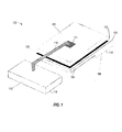
- FIG. 1 illustrates a leadframe having a die-pad with a die mount surface on an upper portion.
- the leadframe 100 includes one die-pad 102 and one lead-pad 110.
- the die-pad 102 has a base portion 106 and an upper portion 104 that extends laterally from the base portion 106.
- a bottom surface 112 of the base portion 106 and a bottom surface 118 of the lead-pad 110 form external contact terminals for the backside of the semiconductor package when packaging is completed.
- a semiconductor die 108 is mounted on a top surface 122 of the die-pad and affixed with a bonding material 120.
- the upper portion 104 of the die-pad 102 extending beyond the base portion 106 provides an area for die mounting that is greater in size than an area provided if only an area comparable in size to the base portion 106 were provided.
- contact pads 114 of the semiconductor die 108 are electrically coupled to lead-pads 110 with a wirebond 116.
- the base portion 106 of the die-pad 102 rests on an assembly surface during packaging. As discussed above, due to a particular design and associated design rules, the base portion 106 of the die-pad 102 may not provide adequate support for the die-pad. As a result, the weight of the semiconductor die 108 on the upper portion 104 or the forces of the wirebonding process may cause the die-pad 102 to tip, or otherwise become unbalanced during packaging.
- the leadframe 100 is implemented to include a support arm (not shown) extending from the upper portion 104 of the die-pad 102 to provide stability to the die-pad during packaging. The support arm is formed in a cutting lane, outside dimensions of the complete packaged semiconductor die, so that the support arm is removed during the packaging process. Because the support arm is not present in the final package, the support arm does not conflict with any restrictions imposed by design rules.
- FIGs. 2-4 show a leadframe having an example support arm structure in the cutting lane.
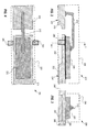
- FIG. 2 shows a side view of a die wirebonded on a leadframe
- FIG. 3 shows cross section I of the die wirebonded on the leadframe shown in FIG. 2
- FIG. 4 shows a top view of the die wirebonded on the leadframe.
- the illustrated leadframe 200 includes a die-pad having a base portion 202 and an upper portion 204.
- a semiconductor die 206 is mounted on the top surface of the die-pad, and a portion of the semiconductor die occupies an area of the upper portion 204 that is unsupported by the base portion 202.
- a contact of the semiconductor die 206 is wirebonded to a lead-pad 210 via wirebond 212.
- the wirebond 212 and lead-pad 210 form an electrical path from an external contact area on the bottom surface 232 of the lead-pad 210 to the semiconductor die 206.
- Block 230 in FIGs. 2, 3, and 4 shows the outline of what will eventually be the completed package after singulation.
- a support arm 208 extends from and provides support for the upper portion 204. Prior to singulation of the package, the support arm 208 extends beyond the package outline 230 ( FIGs. 3 and 4 ). In this embodiment, the support arm 208 extends laterally from the side of the upper portion 206, as shown in FIGs. 3 and 4 , and downward to an extent that is generally co-planar with bottom surfaces 234 and 232 of the base portion 202 and lead-pad 210, respectively. Because the support arm 208 extends beyond the dimensions of the completed package 230, the support arm can be removed during singulation of multiple packages. Thus, once the packages have been singulated the support arms will have been removed and will not violate any design rules regulating contact area and location of the die-pad 202 and lead-pad 210
- base portion 202 and upper portion 204 of the die-pad are depicted as separate elements. It will be appreciated that the base portion 202 and upper portion 204 may be a monolithic structure. Likewise, support arm 208 may be integrally formed as part of the die-pad. Alternatively, the portions and support arm may be formed separately and attached as shown.
- the die-pad may be electrically coupled to a contact pad on the bottom of the semiconductor die.
- the die contact may be electrically coupled to the die-pad using a conductive bonding substance, such as a conductive adhesive or a solderable material such as solder paste or solder.
- a contact pad of the semiconductor die may be wirebonded to the die-pad.
- FIG. 5 shows a flowchart of a method for packaging a semiconductor die.
- Die-pads and lead-pad(s) of leadframes are oriented on a manufacturing surface at process block 502.
- die-pads and lead-pads of leadframes may be pre-oriented and provided on support tape for ease of manufacturing.
- Semiconductor dice are bonded to the die-pads at block 504.
- the contacts of each die are wirebonded to lead-pads of the respective leadframe at block 506.
- the dice and leadframes are encapsulated in packaging material at block 508.
- Support tape, if used, is removed at block 510.
- the encapsulated dice and leadframes are cut into separate packages (singulated) at block 512. As a result of singulation, the support arms will have been removed from the finished package.
- FIGs. 6-10 illustrate packaging a plurality of semiconductor dice according to the process shown in FIG. 5 .
- FIG. 6 shows a plurality of leadframes arranged in a row prior to diebonding.
- each leadframe for example, leadframe 710, is illustrated in cross section similar to that shown in FIG. 3 .
- Each leadframe includes a die-pad having base portion 702 and an upper portion 704 that extends laterally from the base portion.
- a support arm 708 extends from and supports the upper portion of the die-pad.
- the leadframes are attached to support tape 712.
- FIG. 7 illustrates mounting and wirebonding semiconductor dice on the plurality of leadframes shown in FIG. 6 .
- a semiconductor die 722 is mounted on the upper portion 704 of the die-pad. Contacts of the dice are wirebonded, via wirebonds 724, to one or more lead-pads (not shown).
- FIG. 8 illustrates encapsulation of the leadframes and dice in packaging material, such as a resin polymer.
- packaging material such as a resin polymer.
- the die package is stabilized and sealed by applying packaging material over the leadframe carrier and dice by any suitable molding technique known in the art.
- the body may be applied to the carrier by molding in a suitable mold tray.
- the package material body may be formed by transfer or injection molding over the carrier.
- the packaging material body fully encapsulates the die-pad, die, and lead pad, filling any open spaces within the package dimensions, without covering the bottom surfaces of the die-pad and lead-pad since they are adhered to the tape 712.
- the bottom surfaces form external contacts on the backside of the package.
- the body of package material is cured and at least partially hardened, using techniques that are also known in the art, such as oven curing.
- the leadframes are encapsulated together, with the packaging material filling the areas in the cutting lanes between the leadframes.
- a portion of the support arm may be left exposed and not encased by packaging material.
- FIG. 9 illustrates removal of support tape 712 from the plurality 902 of encapsulated leadframes and dice after curing.
- FIG. 10 illustrates separation of the encapsulated leadframes into separate electronic packages.
- the packages, each of which includes one semiconductor die, are separated or singulated along a cutting lane 1004 between the individual ones of packages 1002. The singulation may be performed using techniques known to those skilled in the art. Once singulated, the packages may be electrically mounted to a substrate or printed circuit board.
- FIGs. 11-13 show a leadframe having an alternative structure for a support arm.
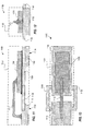
- FIG. 11 shows a side view of a die wirebonded on a leadframe
- FIG. 12 shows a front view of the die wirebonded on the leadframe shown in FIG. 11
- FIG. 13 shows a top view of the die wirebonded on the leadframe shown in FIG. 11
- the illustrated leadframe includes a die-pad having a base portion 1102 and an upper portion 1104. The upper portion extends laterally from the base portion. A bottom surface 1134 of the base portion 1102 of the die-pad and a bottom surface 1132 of the lead-pad 1110 form external contact terminals on the backside of the package when the package is complete.
- a semiconductor die 1106 is mounted on the upper portion 1104 of the die-pad.
- the die 1106 is wirebonded to a lead-pad contact 1110 via wirebond 1112.
- a support arm 1108 supports a part of the upper portion 1104 that is not supported by the base portion 1102. The support is provided by way of the support arm being attached to both the upper portion 1104 and to the lead-pad 1110. A portion of the support arm 1108 is located in the cutting lane. In this manner, when the packages are singulated, the die-pad will not be electrically coupled to the lead-pad 1110 via the support arm.
Landscapes
- Lead Frames For Integrated Circuits (AREA)
- Structures Or Materials For Encapsulating Or Coating Semiconductor Devices Or Solid State Devices (AREA)
Abstract
Description
- One of the major trends in the semiconductor packaging industry is to use surface-mount technology (SMT) as a replacement for conventional plated-through-hole (PTH) technology. SMT offers several distinct advantages over PTH technology, such as greater packaging density, higher lead counts with shorter interconnection lengths and easier automation. Since SMT requires electronic devices and components to be mountable on the surface of a printed circuit board (PCB) or substrate, the materials and structure of traditional through-hole components including capacitors, resistors, and inductors have to be redesigned to meet the modern-day demand for short, thin, light, and small electronic devices. Examples of semiconductor devices accomplishing these objects include quad flat non-leaded packages. Quad flat non-leaded packages have a package structure in which space-consuming outer leads protruding laterally out of a package are eliminated. Instead, external electrode pads to be electrically connected to a circuit board are provided on the bottom surface of the quad flat non-leaded package. The bottom surface of the package that connects to the circuit board may be referred to as the backside of the package as used herein.
- A quad flat non-leaded package, especially a leadless leadframe package, makes use of a metal leadframe as a support structure in the packaging of a semiconductor die. Typically a plurality of leadframes are provided together in a strip of leadframes for packaging multiple dice. Each leadframe includes a die attach pad (die-pad) and one or more contacts (lead-pads) disposed about the leadframe. During assembly, dice are attached to the respective die-pads and wire bonding is used to electrically couple contacts of each die to their associated lead-pads. Wirebonding may be performed using a number of different methods including ball bonding, wedge bonding, etc. As used herein wirebonding is generically used to refer to various methods known in the art used to electrically couple contacts of a die to associated lead-pads. After the wire bonding process, the leadframes and dice are encapsulated by molding a packaging material, for example, a resin, over the top surface of the wire-bonded dice and leadframes. The encapsulated leadless leadframe packages are then singulated using conventional sawing. The packaged die may then be mounted on a printed circuit board (PCB). When mounted, the bottom surface of lead-pads and/or die-pads on the backside of the package connect with PCB contacts to connect the die with PBC circuitry.
- The area of the die-pads and lead-pads on the backside of the package may be restricted to meet a set of design and layout rules. A design rule set specifies certain geometric and connectivity restrictions to ensure sufficient margins to account for variability in the manufacturing processes, ensure various electrical characteristics, and reduce area requirements of a circuit. However, it may be desirable to have a semiconductor die that is larger than the allowed area for the contact on the backside of the die-pad.
- One or more embodiments may address one or more of the above issues.
- In one embodiment, a method is provided for packaging a semiconductor die. A leadframe having a die-pad and one or more lead-pads is placed on an assembly surface. The die-pad has a base portion resting on the assembly surface, an upper portion on the base portion extending laterally from the base portion, and a support arm extending from and supporting the upper portion of die-pad. A semiconductor die is bonded to a top surface of the upper portion of the die-pad. The semiconductor die is wire bonded to the one or more lead-pads. The semiconductor die and leadframe are encased in a package material. The package material fills a space between the upper portion of the die-pad and the assembly surface. A portion of the support arm is removed.
- In another embodiment, an intermediate structure is provided for making an electronic package. The intermediate structure includes a die-pad having a base portion and an upper portion above and extending laterally from the base portion. A semiconductor die is mounted on a top surface of the upper portion of the die-pad. A support arm extends from and supports the upper portion of the die-pad. The support arm extends beyond an area defined by the outline of the electronic package.
- In yet another embodiment, an article of manufacture is provided. The article is characterized by a plurality of electronic packages arranged in a row or matrix. Each one of the electronic packages includes a die-pad and a semiconductor die mounted on a top surface of the die-pad. Between pairs of adjacent die-pads, respective connection arms connect the pairs of die-pads. A support arm extends from each connection arm and provides support for the die-pads connected thereto. The support arm extends into a cutting lane of the plurality of the electronic packages.
- The above discussion is not intended to describe each embodiment or every implementation. Various example embodiments may be more completely understood in consideration of the following detailed description in connection with the accompanying drawings, in which:
-
FIG. 1 shows a perspective view of a die wirebonded on a leadframe; -
FIG. 2 shows a side view of a die wirebonded on a leadframe; -
FIG. 3 shows cross-section I, of the die wirebonded on the leadframe shown in -
FIG. 2 ; -
FIG. 4 shows a top view of the die wirebonded on the leadframe shown inFIG. 2 ; -
FIG. 5 shows a flowchart of a method for packaging a semiconductor die; -
FIG. 6 shows a plurality of leadframes arranged in a row; -
FIG. 7 illustrates mounting and wirebonding semiconductor dice on the plurality of leadframes shown inFIG. 6 ; -
FIG. 8 illustrates encapsulation of the leadframes and dice in package material; -
FIG. 9 illustrates removal of support tape from the encapsulated leadframes; -
FIG. 10 illustrates separation of the encapsulated leadframes into separate electronic packages; -
FIG. 11 shows a side view of a die wirebonded on a leadframe; -
FIG. 12 shows a front view of the die wirebonded on the leadframe shown inFIG. 11 ; and -
FIG. 13 shows a top view of the die wirebonded on the leadframe shown inFIG. 11 . - While the disclosure is amenable to various modifications and alternative forms, examples thereof have been shown by way of example in the drawings and will be described in detail. It should be understood, however, that the intention is not to limit the disclosure to the particular embodiments shown and/or described. On the contrary, the intention is to cover all modifications, equivalents, and alternatives falling within the spirit and scope of the disclosure.
- In one or more embodiments, a leadframe and method for die packaging are provided. The leadframe and method utilize one or more lead-pads and one or more die-pads. Each die-pad includes a base portion and an upper portion over the base portion. The upper portion is larger than the base portion and provides a die mounting surface that is larger than a die mounting surface that would be available with just the base portion. The upper portion extends laterally from the base portion. During assembly, however, the part of the upper portion that extends from the base portion may cause the die-pad to become unbalanced or unstable during the wirebonding and packaging processes. In one or more embodiments, a support arm is disposed in a cutting lane between die packages. The support arm provides support and increases stability of the die-pad during the wirebonding process. Once the die and die-pad are encapsulated in packaging material, support arms located in the cutting lanes are removed as a result of singulation of the packages.
- It is recognized that the leadframe may include any number of die-pads and lead-pads to provide external contacts for respective contact pads of the die(s) included in each package. For ease of explanation, the embodiments and examples are primarily described with reference to a semiconductor package having two external contacts formed by a bottom surface of one die-pad and a bottom surface of one lead-pad.
-
FIG. 1 illustrates a leadframe having a die-pad with a die mount surface on an upper portion. In this example, theleadframe 100 includes one die-pad 102 and one lead-pad 110. The die-pad 102 has abase portion 106 and anupper portion 104 that extends laterally from thebase portion 106. Abottom surface 112 of thebase portion 106 and abottom surface 118 of the lead-pad 110 form external contact terminals for the backside of the semiconductor package when packaging is completed. A semiconductor die 108 is mounted on atop surface 122 of the die-pad and affixed with abonding material 120. Theupper portion 104 of the die-pad 102 extending beyond thebase portion 106 provides an area for die mounting that is greater in size than an area provided if only an area comparable in size to thebase portion 106 were provided. During packaging,contact pads 114 of the semiconductor die 108 are electrically coupled to lead-pads 110 with awirebond 116. - The
base portion 106 of the die-pad 102 rests on an assembly surface during packaging. As discussed above, due to a particular design and associated design rules, thebase portion 106 of the die-pad 102 may not provide adequate support for the die-pad. As a result, the weight of the semiconductor die 108 on theupper portion 104 or the forces of the wirebonding process may cause the die-pad 102 to tip, or otherwise become unbalanced during packaging. In one or more embodiments, theleadframe 100 is implemented to include a support arm (not shown) extending from theupper portion 104 of the die-pad 102 to provide stability to the die-pad during packaging. The support arm is formed in a cutting lane, outside dimensions of the complete packaged semiconductor die, so that the support arm is removed during the packaging process. Because the support arm is not present in the final package, the support arm does not conflict with any restrictions imposed by design rules. - Various structures for supporting the die-pad may be located in the cutting lane, and outside the dimensions of what will eventually be the completed package.
FIGs. 2-4 show a leadframe having an example support arm structure in the cutting lane.FIG. 2 shows a side view of a die wirebonded on a leadframe,FIG. 3 shows cross section I of the die wirebonded on the leadframe shown inFIG. 2, and FIG. 4 shows a top view of the die wirebonded on the leadframe. The illustratedleadframe 200 includes a die-pad having abase portion 202 and anupper portion 204. In this example illustration, asemiconductor die 206 is mounted on the top surface of the die-pad, and a portion of the semiconductor die occupies an area of theupper portion 204 that is unsupported by thebase portion 202. A contact of the semiconductor die 206 is wirebonded to a lead-pad 210 viawirebond 212. Thewirebond 212 and lead-pad 210 form an electrical path from an external contact area on thebottom surface 232 of the lead-pad 210 to the semiconductor die 206. -
Block 230 inFIGs. 2, 3, and 4 shows the outline of what will eventually be the completed package after singulation. Asupport arm 208 extends from and provides support for theupper portion 204. Prior to singulation of the package, thesupport arm 208 extends beyond the package outline 230 (FIGs. 3 and 4 ). In this embodiment, thesupport arm 208 extends laterally from the side of theupper portion 206, as shown inFIGs. 3 and 4 , and downward to an extent that is generally co-planar withbottom surfaces base portion 202 and lead-pad 210, respectively. Because thesupport arm 208 extends beyond the dimensions of the completedpackage 230, the support arm can be removed during singulation of multiple packages. Thus, once the packages have been singulated the support arms will have been removed and will not violate any design rules regulating contact area and location of the die-pad 202 and lead-pad 210 - For purposes of explanation,
base portion 202 andupper portion 204 of the die-pad are depicted as separate elements. It will be appreciated that thebase portion 202 andupper portion 204 may be a monolithic structure. Likewise,support arm 208 may be integrally formed as part of the die-pad. Alternatively, the portions and support arm may be formed separately and attached as shown. - In some embodiments, the die-pad may be electrically coupled to a contact pad on the bottom of the semiconductor die. For example, the die contact may be electrically coupled to the die-pad using a conductive bonding substance, such as a conductive adhesive or a solderable material such as solder paste or solder. In some other embodiments, a contact pad of the semiconductor die may be wirebonded to the die-pad.
-
FIG. 5 shows a flowchart of a method for packaging a semiconductor die. Die-pads and lead-pad(s) of leadframes are oriented on a manufacturing surface atprocess block 502. In some implementations, die-pads and lead-pads of leadframes may be pre-oriented and provided on support tape for ease of manufacturing. Semiconductor dice are bonded to the die-pads atblock 504. The contacts of each die are wirebonded to lead-pads of the respective leadframe atblock 506. The dice and leadframes are encapsulated in packaging material atblock 508. Support tape, if used, is removed atblock 510. The encapsulated dice and leadframes are cut into separate packages (singulated) atblock 512. As a result of singulation, the support arms will have been removed from the finished package. -
FIGs. 6-10 illustrate packaging a plurality of semiconductor dice according to the process shown inFIG. 5 .FIG. 6 shows a plurality of leadframes arranged in a row prior to diebonding. In this example illustration, each leadframe, for example,leadframe 710, is illustrated in cross section similar to that shown inFIG. 3 . Each leadframe includes a die-pad havingbase portion 702 and anupper portion 704 that extends laterally from the base portion. Asupport arm 708 extends from and supports the upper portion of the die-pad. In this example, the leadframes are attached to supporttape 712. -
FIG. 7 illustrates mounting and wirebonding semiconductor dice on the plurality of leadframes shown inFIG. 6 . A semiconductor die 722 is mounted on theupper portion 704 of the die-pad. Contacts of the dice are wirebonded, viawirebonds 724, to one or more lead-pads (not shown). -
FIG. 8 illustrates encapsulation of the leadframes and dice in packaging material, such as a resin polymer. The die package is stabilized and sealed by applying packaging material over the leadframe carrier and dice by any suitable molding technique known in the art. For example, the body may be applied to the carrier by molding in a suitable mold tray. For example, the package material body may be formed by transfer or injection molding over the carrier. The packaging material body fully encapsulates the die-pad, die, and lead pad, filling any open spaces within the package dimensions, without covering the bottom surfaces of the die-pad and lead-pad since they are adhered to thetape 712. The bottom surfaces form external contacts on the backside of the package. The body of package material is cured and at least partially hardened, using techniques that are also known in the art, such as oven curing. - In this illustrative example, the leadframes are encapsulated together, with the packaging material filling the areas in the cutting lanes between the leadframes. In some embodiments, a portion of the support arm may be left exposed and not encased by packaging material.
-
FIG. 9 illustrates removal ofsupport tape 712 from theplurality 902 of encapsulated leadframes and dice after curing.FIG. 10 illustrates separation of the encapsulated leadframes into separate electronic packages. The packages, each of which includes one semiconductor die, are separated or singulated along acutting lane 1004 between the individual ones ofpackages 1002. The singulation may be performed using techniques known to those skilled in the art. Once singulated, the packages may be electrically mounted to a substrate or printed circuit board. -
FIGs. 11-13 show a leadframe having an alternative structure for a support arm. -
FIG. 11 shows a side view of a die wirebonded on a leadframe,FIG. 12 shows a front view of the die wirebonded on the leadframe shown inFIG. 11, and FIG. 13 shows a top view of the die wirebonded on the leadframe shown inFIG. 11 . The illustrated leadframe includes a die-pad having abase portion 1102 and anupper portion 1104. The upper portion extends laterally from the base portion. Abottom surface 1134 of thebase portion 1102 of the die-pad and abottom surface 1132 of the lead-pad 1110 form external contact terminals on the backside of the package when the package is complete. In this example illustration, asemiconductor die 1106 is mounted on theupper portion 1104 of the die-pad. Thedie 1106 is wirebonded to a lead-pad contact 1110 viawirebond 1112. Asupport arm 1108 supports a part of theupper portion 1104 that is not supported by thebase portion 1102. The support is provided by way of the support arm being attached to both theupper portion 1104 and to the lead-pad 1110. A portion of thesupport arm 1108 is located in the cutting lane. In this manner, when the packages are singulated, the die-pad will not be electrically coupled to the lead-pad 1110 via the support arm. - Based upon the above discussion and illustrations, those skilled in the art will readily recognize that various modifications and changes may be made without strictly following the exemplary embodiments and applications illustrated and described herein. Such modifications do not depart from the true spirit and scope of the present disclosure, including that set forth in the following claims.
Claims (20)
- A method of packaging a semiconductor die, the method comprising:placing (502) a leadframe on an assembly surface, the leadframe having a die-pad (202/204) and one or more lead-pads (210), the die-pad having a base portion (202) resting on the assembly surface, an upper portion (204) on the base portion extending laterally from the base portion, and a support arm (208) extending from and supporting the upper portion of die-pad;bonding (504) a semiconductor die (206) to a top surface of the upper portion of the die-pad;wirebonding (506) the semiconductor die to the one or more lead-pads (210);encasing (508) the semiconductor die and leadframe in a package material (802), the package material filling a space between the upper portion of the die-pad and the assembly surface; andremoving (512) a portion of the support arm.
- The method of claim 1, wherein the support arm extends from the upper portion of the die-pad down to the assembly surface.
- The method of claim 1, wherein the support arm couples the upper portion of the die-pad to one of the one or more lead-pads.
- The method of claim 1, wherein the support arm couples the upper portion of the first mentioned die-pad to a second die pad.
- The method of claim 1, wherein:encasing the semiconductor die and leadframe in the package material encases the support arm in the package material; andremoving the portion of the support arm includes removing a portion of the package material extending outside an area defined by dimensions of the packaged semiconductor die.
- The method of claim 1, wherein encasing the semiconductor die and leadframe in the package material leaves the portion of the support arm, extending outside an area defined by the dimensions of the packaged semiconductor die, exposed.
- The method of claim 1, wherein the die-pad has at least a second support arm extending from the upper portion of the die-pad.
- The method of claim 7, wherein the second support arm extends from the upper portion in a direction opposite of the first mentioned support arm.
- The method of claim 1, wherein:the leadframe is coupled to a second like leadframe via the support arm; andthe portion of the support arm is removed by a process that includes separating the first mentioned leadframe from second like leadframe.
- An intermediate structure for making an electronic package, comprising:a die-pad having a base portion (202) and an upper portion (204) above and extending laterally from the base portion;a semiconductor die (206) mounted on a top surface of the upper portion of the die-pad; anda support arm (208) extending from and supporting the upper portion of the die-pad, the support arm extending beyond an area (230) defined by the electronic package.
- The leadframe structure of claim 10, wherein the support arm extends from the upper portion of the die-pad to a plane of a bottom surface of the base portion of the die-pad.
- The leadframe structure of claim 10, wherein the support arm couples the upper portion of the die-pad to a lead-pad.
- The leadframe structure of claim 10, wherein the support arm couples the upper portion of the first mentioned die-pad to a second die pad.
- The leadframe structure of claim 12, wherein the lead pad is wirebonded to the semiconductor die.
- An article of manufacture, comprising:a plurality of electronic packages (710) arranged in a row and matrix, each package including:a die-pad (702/704); anda semiconductor die (722) mounted on a top surface of the die-pad;between pairs of adjacent die-pads, respective connection arms connecting the pairs of die-pads; anda support arm (708) extending from each connection arm and providing support for the die-pads connected thereto, the support arm extending into a cutting lane (1004) of the plurality of the electronic packages.
- The article of claim 15, wherein each package further includes one or more lead-pads wirebonded to the semiconductor die of the package.
- The article of claim15, wherein the support arm couples the die-pad to one of the lead-pads of one of the plurality of semiconductor devices.
- The article of claim 15, wherein the support arm extends from the connection arm to a plane encompassing the bottom surface of the die-pad.
- The article of claim 15, wherein the support arm couples the connection arm to a lead-pad of one of the plurality of electronic packages.
- The article of claim 15, wherein the die-pad and semiconductor die together have a center of mass that is not oriented above a base of the die-pad.
Priority Applications (3)
| Application Number | Priority Date | Filing Date | Title |
|---|---|---|---|
| EP11165403.4A EP2523211B1 (en) | 2011-05-10 | 2011-05-10 | Leadframe and method for packaging semiconductor die |
| CN201210139755.0A CN102779761B (en) | 2011-05-10 | 2012-05-08 | Leadframe and method for packaging semiconductor die |
| US13/466,926 US20120286399A1 (en) | 2011-05-10 | 2012-05-08 | Leadframe and method for packaging semiconductor die |
Applications Claiming Priority (1)
| Application Number | Priority Date | Filing Date | Title |
|---|---|---|---|
| EP11165403.4A EP2523211B1 (en) | 2011-05-10 | 2011-05-10 | Leadframe and method for packaging semiconductor die |
Publications (2)
| Publication Number | Publication Date |
|---|---|
| EP2523211A1 true EP2523211A1 (en) | 2012-11-14 |
| EP2523211B1 EP2523211B1 (en) | 2019-10-23 |
Family
ID=44483824
Family Applications (1)
| Application Number | Title | Priority Date | Filing Date |
|---|---|---|---|
| EP11165403.4A Active EP2523211B1 (en) | 2011-05-10 | 2011-05-10 | Leadframe and method for packaging semiconductor die |
Country Status (3)
| Country | Link |
|---|---|
| US (1) | US20120286399A1 (en) |
| EP (1) | EP2523211B1 (en) |
| CN (1) | CN102779761B (en) |
Families Citing this family (4)
| Publication number | Priority date | Publication date | Assignee | Title |
|---|---|---|---|---|
| CN109065519B (en) * | 2018-06-13 | 2020-12-25 | 南通通富微电子有限公司 | Semiconductor chip packaging device |
| CN109037078A (en) * | 2018-06-13 | 2018-12-18 | 南通通富微电子有限公司 | A kind of semiconductor chip packaging method |
| CN109037183A (en) * | 2018-06-13 | 2018-12-18 | 南通通富微电子有限公司 | A kind of semiconductor chip packaging array and semiconductor chip packaging device |
| CN109065518B (en) * | 2018-06-13 | 2020-12-25 | 南通通富微电子有限公司 | Semiconductor chip packaging array |
Citations (5)
| Publication number | Priority date | Publication date | Assignee | Title |
|---|---|---|---|---|
| US5577617A (en) * | 1995-12-29 | 1996-11-26 | Xerox Corporation | Advanced technique for packaging multiple number of electrically stackable high voltage transistors in one package |
| US20010035569A1 (en) * | 2000-05-01 | 2001-11-01 | Rohm Co.,Ltd | Resin-packaged semiconductor device |
| US20030071344A1 (en) * | 2001-10-16 | 2003-04-17 | Shinko Electric Industries Co., Ltd. | Leadframe and method of manufacturing a semiconductor device using the same |
| US20040070056A1 (en) * | 2002-08-06 | 2004-04-15 | Hideki Matsuzawa | Lead frame and method of manufacturing the same |
| US20080135996A1 (en) * | 2006-09-22 | 2008-06-12 | Yamaha Corporation | Lead frame |
Family Cites Families (4)
| Publication number | Priority date | Publication date | Assignee | Title |
|---|---|---|---|---|
| JP2003086750A (en) * | 2001-09-11 | 2003-03-20 | Rohm Co Ltd | Manufacturing method of electronic components |
| WO2006090304A1 (en) * | 2005-02-23 | 2006-08-31 | Nxp B.V. | An integrated circuit package device with improved bond pad connections, a leadframe and an electronic device |
| US7629676B2 (en) * | 2006-09-07 | 2009-12-08 | Infineon Technologies Ag | Semiconductor component having a semiconductor die and a leadframe |
| US7683463B2 (en) * | 2007-04-19 | 2010-03-23 | Fairchild Semiconductor Corporation | Etched leadframe structure including recesses |
-
2011
- 2011-05-10 EP EP11165403.4A patent/EP2523211B1/en active Active
-
2012
- 2012-05-08 US US13/466,926 patent/US20120286399A1/en not_active Abandoned
- 2012-05-08 CN CN201210139755.0A patent/CN102779761B/en active Active
Patent Citations (5)
| Publication number | Priority date | Publication date | Assignee | Title |
|---|---|---|---|---|
| US5577617A (en) * | 1995-12-29 | 1996-11-26 | Xerox Corporation | Advanced technique for packaging multiple number of electrically stackable high voltage transistors in one package |
| US20010035569A1 (en) * | 2000-05-01 | 2001-11-01 | Rohm Co.,Ltd | Resin-packaged semiconductor device |
| US20030071344A1 (en) * | 2001-10-16 | 2003-04-17 | Shinko Electric Industries Co., Ltd. | Leadframe and method of manufacturing a semiconductor device using the same |
| US20040070056A1 (en) * | 2002-08-06 | 2004-04-15 | Hideki Matsuzawa | Lead frame and method of manufacturing the same |
| US20080135996A1 (en) * | 2006-09-22 | 2008-06-12 | Yamaha Corporation | Lead frame |
Also Published As
| Publication number | Publication date |
|---|---|
| US20120286399A1 (en) | 2012-11-15 |
| EP2523211B1 (en) | 2019-10-23 |
| CN102779761A (en) | 2012-11-14 |
| CN102779761B (en) | 2015-04-01 |
Similar Documents
| Publication | Publication Date | Title |
|---|---|---|
| US7816769B2 (en) | Stackable packages for three-dimensional packaging of semiconductor dice | |
| US7932587B2 (en) | Singulated semiconductor package | |
| US7348659B2 (en) | Semiconductor device and method of manufacturing thereof | |
| US20030006055A1 (en) | Semiconductor package for fixed surface mounting | |
| US20010017410A1 (en) | Mounting multiple semiconductor dies in a package | |
| JPH0546045U (en) | Semiconductor package | |
| US8963302B2 (en) | Stacked packaged integrated circuit devices, and methods of making same | |
| US9324637B1 (en) | Quad flat non-leaded semiconductor package with wettable flank | |
| CN117558699A (en) | SMD integration on QFN via 3D stacking solution | |
| US10090228B1 (en) | Semiconductor device with leadframe configured to facilitate reduced burr formation | |
| US8368192B1 (en) | Multi-chip memory package with a small substrate | |
| US10636735B2 (en) | Package structure and the method to fabricate thereof | |
| US11227820B2 (en) | Through hole side wettable flank | |
| CN1937194A (en) | Method of making stacked die package | |
| US10290593B2 (en) | Method of assembling QFP type semiconductor device | |
| EP2523211B1 (en) | Leadframe and method for packaging semiconductor die | |
| JP2002198482A (en) | Semiconductor device and method of manufacturing the same | |
| US20040021231A1 (en) | Semiconductor device and its manufacturing method | |
| US20110108967A1 (en) | Semiconductor chip grid array package and method for fabricating same | |
| JPH11297917A (en) | Semiconductor device and manufacturing method thereof | |
| CN101378023B (en) | Semiconductor package and fabrication method thereof | |
| KR101432486B1 (en) | Method for manufacturing of integrated circuit package | |
| US20260123458A1 (en) | Ic package structure with connections and method of manufacturing the same | |
| KR100537893B1 (en) | Leadframe and multichip package using the same | |
| EP4657521A1 (en) | A method of fabricating a semiconductor integrated circuits package |
Legal Events
| Date | Code | Title | Description |
|---|---|---|---|
| PUAI | Public reference made under article 153(3) epc to a published international application that has entered the european phase |
Free format text: ORIGINAL CODE: 0009012 |
|
| AK | Designated contracting states |
Kind code of ref document: A1 Designated state(s): AL AT BE BG CH CY CZ DE DK EE ES FI FR GB GR HR HU IE IS IT LI LT LU LV MC MK MT NL NO PL PT RO RS SE SI SK SM TR |
|
| AX | Request for extension of the european patent |
Extension state: BA ME |
|
| 17P | Request for examination filed |
Effective date: 20130514 |
|
| 17Q | First examination report despatched |
Effective date: 20140710 |
|
| RAP1 | Party data changed (applicant data changed or rights of an application transferred) |
Owner name: NEXPERIA B.V. |
|
| STAA | Information on the status of an ep patent application or granted ep patent |
Free format text: STATUS: EXAMINATION IS IN PROGRESS |
|
| GRAP | Despatch of communication of intention to grant a patent |
Free format text: ORIGINAL CODE: EPIDOSNIGR1 |
|
| STAA | Information on the status of an ep patent application or granted ep patent |
Free format text: STATUS: GRANT OF PATENT IS INTENDED |
|
| RIC1 | Information provided on ipc code assigned before grant |
Ipc: H01L 21/56 20060101AFI20190510BHEP Ipc: H01L 23/31 20060101ALI20190510BHEP Ipc: H01L 23/00 20060101ALI20190510BHEP Ipc: H01L 23/495 20060101ALI20190510BHEP |
|
| INTG | Intention to grant announced |
Effective date: 20190605 |
|
| GRAS | Grant fee paid |
Free format text: ORIGINAL CODE: EPIDOSNIGR3 |
|
| GRAA | (expected) grant |
Free format text: ORIGINAL CODE: 0009210 |
|
| STAA | Information on the status of an ep patent application or granted ep patent |
Free format text: STATUS: THE PATENT HAS BEEN GRANTED |
|
| AK | Designated contracting states |
Kind code of ref document: B1 Designated state(s): AL AT BE BG CH CY CZ DE DK EE ES FI FR GB GR HR HU IE IS IT LI LT LU LV MC MK MT NL NO PL PT RO RS SE SI SK SM TR |
|
| REG | Reference to a national code |
Ref country code: GB Ref legal event code: FG4D |
|
| REG | Reference to a national code |
Ref country code: CH Ref legal event code: EP |
|
| REG | Reference to a national code |
Ref country code: IE Ref legal event code: FG4D |
|
| REG | Reference to a national code |
Ref country code: DE Ref legal event code: R096 Ref document number: 602011062855 Country of ref document: DE |
|
| REG | Reference to a national code |
Ref country code: AT Ref legal event code: REF Ref document number: 1194643 Country of ref document: AT Kind code of ref document: T Effective date: 20191115 |
|
| REG | Reference to a national code |
Ref country code: NL Ref legal event code: MP Effective date: 20191023 |
|
| REG | Reference to a national code |
Ref country code: LT Ref legal event code: MG4D |
|
| PG25 | Lapsed in a contracting state [announced via postgrant information from national office to epo] |
Ref country code: PL Free format text: LAPSE BECAUSE OF FAILURE TO SUBMIT A TRANSLATION OF THE DESCRIPTION OR TO PAY THE FEE WITHIN THE PRESCRIBED TIME-LIMIT Effective date: 20191023 Ref country code: NO Free format text: LAPSE BECAUSE OF FAILURE TO SUBMIT A TRANSLATION OF THE DESCRIPTION OR TO PAY THE FEE WITHIN THE PRESCRIBED TIME-LIMIT Effective date: 20200123 Ref country code: LT Free format text: LAPSE BECAUSE OF FAILURE TO SUBMIT A TRANSLATION OF THE DESCRIPTION OR TO PAY THE FEE WITHIN THE PRESCRIBED TIME-LIMIT Effective date: 20191023 Ref country code: BG Free format text: LAPSE BECAUSE OF FAILURE TO SUBMIT A TRANSLATION OF THE DESCRIPTION OR TO PAY THE FEE WITHIN THE PRESCRIBED TIME-LIMIT Effective date: 20200123 Ref country code: NL Free format text: LAPSE BECAUSE OF FAILURE TO SUBMIT A TRANSLATION OF THE DESCRIPTION OR TO PAY THE FEE WITHIN THE PRESCRIBED TIME-LIMIT Effective date: 20191023 Ref country code: SE Free format text: LAPSE BECAUSE OF FAILURE TO SUBMIT A TRANSLATION OF THE DESCRIPTION OR TO PAY THE FEE WITHIN THE PRESCRIBED TIME-LIMIT Effective date: 20191023 Ref country code: LV Free format text: LAPSE BECAUSE OF FAILURE TO SUBMIT A TRANSLATION OF THE DESCRIPTION OR TO PAY THE FEE WITHIN THE PRESCRIBED TIME-LIMIT Effective date: 20191023 Ref country code: ES Free format text: LAPSE BECAUSE OF FAILURE TO SUBMIT A TRANSLATION OF THE DESCRIPTION OR TO PAY THE FEE WITHIN THE PRESCRIBED TIME-LIMIT Effective date: 20191023 Ref country code: GR Free format text: LAPSE BECAUSE OF FAILURE TO SUBMIT A TRANSLATION OF THE DESCRIPTION OR TO PAY THE FEE WITHIN THE PRESCRIBED TIME-LIMIT Effective date: 20200124 Ref country code: FI Free format text: LAPSE BECAUSE OF FAILURE TO SUBMIT A TRANSLATION OF THE DESCRIPTION OR TO PAY THE FEE WITHIN THE PRESCRIBED TIME-LIMIT Effective date: 20191023 Ref country code: PT Free format text: LAPSE BECAUSE OF FAILURE TO SUBMIT A TRANSLATION OF THE DESCRIPTION OR TO PAY THE FEE WITHIN THE PRESCRIBED TIME-LIMIT Effective date: 20200224 |
|
| PG25 | Lapsed in a contracting state [announced via postgrant information from national office to epo] |
Ref country code: IS Free format text: LAPSE BECAUSE OF FAILURE TO SUBMIT A TRANSLATION OF THE DESCRIPTION OR TO PAY THE FEE WITHIN THE PRESCRIBED TIME-LIMIT Effective date: 20200224 Ref country code: RS Free format text: LAPSE BECAUSE OF FAILURE TO SUBMIT A TRANSLATION OF THE DESCRIPTION OR TO PAY THE FEE WITHIN THE PRESCRIBED TIME-LIMIT Effective date: 20191023 Ref country code: HR Free format text: LAPSE BECAUSE OF FAILURE TO SUBMIT A TRANSLATION OF THE DESCRIPTION OR TO PAY THE FEE WITHIN THE PRESCRIBED TIME-LIMIT Effective date: 20191023 |
|
| PG25 | Lapsed in a contracting state [announced via postgrant information from national office to epo] |
Ref country code: AL Free format text: LAPSE BECAUSE OF FAILURE TO SUBMIT A TRANSLATION OF THE DESCRIPTION OR TO PAY THE FEE WITHIN THE PRESCRIBED TIME-LIMIT Effective date: 20191023 |
|
| REG | Reference to a national code |
Ref country code: DE Ref legal event code: R097 Ref document number: 602011062855 Country of ref document: DE |
|
| PG2D | Information on lapse in contracting state deleted |
Ref country code: IS |
|
| PG25 | Lapsed in a contracting state [announced via postgrant information from national office to epo] |
Ref country code: DK Free format text: LAPSE BECAUSE OF FAILURE TO SUBMIT A TRANSLATION OF THE DESCRIPTION OR TO PAY THE FEE WITHIN THE PRESCRIBED TIME-LIMIT Effective date: 20191023 Ref country code: EE Free format text: LAPSE BECAUSE OF FAILURE TO SUBMIT A TRANSLATION OF THE DESCRIPTION OR TO PAY THE FEE WITHIN THE PRESCRIBED TIME-LIMIT Effective date: 20191023 Ref country code: CZ Free format text: LAPSE BECAUSE OF FAILURE TO SUBMIT A TRANSLATION OF THE DESCRIPTION OR TO PAY THE FEE WITHIN THE PRESCRIBED TIME-LIMIT Effective date: 20191023 Ref country code: RO Free format text: LAPSE BECAUSE OF FAILURE TO SUBMIT A TRANSLATION OF THE DESCRIPTION OR TO PAY THE FEE WITHIN THE PRESCRIBED TIME-LIMIT Effective date: 20191023 Ref country code: IS Free format text: LAPSE BECAUSE OF FAILURE TO SUBMIT A TRANSLATION OF THE DESCRIPTION OR TO PAY THE FEE WITHIN THE PRESCRIBED TIME-LIMIT Effective date: 20200223 |
|
| REG | Reference to a national code |
Ref country code: AT Ref legal event code: MK05 Ref document number: 1194643 Country of ref document: AT Kind code of ref document: T Effective date: 20191023 |
|
| PLBE | No opposition filed within time limit |
Free format text: ORIGINAL CODE: 0009261 |
|
| STAA | Information on the status of an ep patent application or granted ep patent |
Free format text: STATUS: NO OPPOSITION FILED WITHIN TIME LIMIT |
|
| PG25 | Lapsed in a contracting state [announced via postgrant information from national office to epo] |
Ref country code: SK Free format text: LAPSE BECAUSE OF FAILURE TO SUBMIT A TRANSLATION OF THE DESCRIPTION OR TO PAY THE FEE WITHIN THE PRESCRIBED TIME-LIMIT Effective date: 20191023 Ref country code: IT Free format text: LAPSE BECAUSE OF FAILURE TO SUBMIT A TRANSLATION OF THE DESCRIPTION OR TO PAY THE FEE WITHIN THE PRESCRIBED TIME-LIMIT Effective date: 20191023 Ref country code: SM Free format text: LAPSE BECAUSE OF FAILURE TO SUBMIT A TRANSLATION OF THE DESCRIPTION OR TO PAY THE FEE WITHIN THE PRESCRIBED TIME-LIMIT Effective date: 20191023 |
|
| 26N | No opposition filed |
Effective date: 20200724 |
|
| PG25 | Lapsed in a contracting state [announced via postgrant information from national office to epo] |
Ref country code: AT Free format text: LAPSE BECAUSE OF FAILURE TO SUBMIT A TRANSLATION OF THE DESCRIPTION OR TO PAY THE FEE WITHIN THE PRESCRIBED TIME-LIMIT Effective date: 20191023 Ref country code: SI Free format text: LAPSE BECAUSE OF FAILURE TO SUBMIT A TRANSLATION OF THE DESCRIPTION OR TO PAY THE FEE WITHIN THE PRESCRIBED TIME-LIMIT Effective date: 20191023 |
|
| PG25 | Lapsed in a contracting state [announced via postgrant information from national office to epo] |
Ref country code: LI Free format text: LAPSE BECAUSE OF NON-PAYMENT OF DUE FEES Effective date: 20200531 Ref country code: MC Free format text: LAPSE BECAUSE OF FAILURE TO SUBMIT A TRANSLATION OF THE DESCRIPTION OR TO PAY THE FEE WITHIN THE PRESCRIBED TIME-LIMIT Effective date: 20191023 Ref country code: CH Free format text: LAPSE BECAUSE OF NON-PAYMENT OF DUE FEES Effective date: 20200531 |
|
| REG | Reference to a national code |
Ref country code: BE Ref legal event code: MM Effective date: 20200531 |
|
| GBPC | Gb: european patent ceased through non-payment of renewal fee |
Effective date: 20200510 |
|
| PG25 | Lapsed in a contracting state [announced via postgrant information from national office to epo] |
Ref country code: LU Free format text: LAPSE BECAUSE OF NON-PAYMENT OF DUE FEES Effective date: 20200510 |
|
| PG25 | Lapsed in a contracting state [announced via postgrant information from national office to epo] |
Ref country code: GB Free format text: LAPSE BECAUSE OF NON-PAYMENT OF DUE FEES Effective date: 20200510 Ref country code: FR Free format text: LAPSE BECAUSE OF NON-PAYMENT OF DUE FEES Effective date: 20200531 Ref country code: IE Free format text: LAPSE BECAUSE OF NON-PAYMENT OF DUE FEES Effective date: 20200510 |
|
| PG25 | Lapsed in a contracting state [announced via postgrant information from national office to epo] |
Ref country code: BE Free format text: LAPSE BECAUSE OF NON-PAYMENT OF DUE FEES Effective date: 20200531 |
|
| PG25 | Lapsed in a contracting state [announced via postgrant information from national office to epo] |
Ref country code: TR Free format text: LAPSE BECAUSE OF FAILURE TO SUBMIT A TRANSLATION OF THE DESCRIPTION OR TO PAY THE FEE WITHIN THE PRESCRIBED TIME-LIMIT Effective date: 20191023 Ref country code: MT Free format text: LAPSE BECAUSE OF FAILURE TO SUBMIT A TRANSLATION OF THE DESCRIPTION OR TO PAY THE FEE WITHIN THE PRESCRIBED TIME-LIMIT Effective date: 20191023 Ref country code: CY Free format text: LAPSE BECAUSE OF FAILURE TO SUBMIT A TRANSLATION OF THE DESCRIPTION OR TO PAY THE FEE WITHIN THE PRESCRIBED TIME-LIMIT Effective date: 20191023 |
|
| PG25 | Lapsed in a contracting state [announced via postgrant information from national office to epo] |
Ref country code: MK Free format text: LAPSE BECAUSE OF FAILURE TO SUBMIT A TRANSLATION OF THE DESCRIPTION OR TO PAY THE FEE WITHIN THE PRESCRIBED TIME-LIMIT Effective date: 20191023 |
|
| PGFP | Annual fee paid to national office [announced via postgrant information from national office to epo] |
Ref country code: DE Payment date: 20250528 Year of fee payment: 15 |
|
| REG | Reference to a national code |
Ref country code: DE Ref legal event code: R079 Ref document number: 602011062855 Country of ref document: DE Free format text: PREVIOUS MAIN CLASS: H01L0021560000 Ipc: H10W0074010000 |