EP2520632A2 - Compound for organic photoelectric device and organic photoelectric device including the compound - Google Patents
Compound for organic photoelectric device and organic photoelectric device including the compound Download PDFInfo
- Publication number
- EP2520632A2 EP2520632A2 EP10841123A EP10841123A EP2520632A2 EP 2520632 A2 EP2520632 A2 EP 2520632A2 EP 10841123 A EP10841123 A EP 10841123A EP 10841123 A EP10841123 A EP 10841123A EP 2520632 A2 EP2520632 A2 EP 2520632A2
- Authority
- EP
- European Patent Office
- Prior art keywords
- group
- substituted
- unsubstituted
- photoelectric device
- organic photoelectric
- Prior art date
- Legal status (The legal status is an assumption and is not a legal conclusion. Google has not performed a legal analysis and makes no representation as to the accuracy of the status listed.)
- Withdrawn
Links
- 0 CC(C*1CC1)(CC1)CC2C1C=CCC2 Chemical compound CC(C*1CC1)(CC1)CC2C1C=CCC2 0.000 description 3
Images




Classifications
-
- C—CHEMISTRY; METALLURGY
- C09—DYES; PAINTS; POLISHES; NATURAL RESINS; ADHESIVES; COMPOSITIONS NOT OTHERWISE PROVIDED FOR; APPLICATIONS OF MATERIALS NOT OTHERWISE PROVIDED FOR
- C09K—MATERIALS FOR MISCELLANEOUS APPLICATIONS, NOT PROVIDED FOR ELSEWHERE
- C09K11/00—Luminescent materials, e.g. electroluminescent or chemiluminescent
- C09K11/06—Luminescent materials, e.g. electroluminescent or chemiluminescent containing organic luminescent materials
-
- C—CHEMISTRY; METALLURGY
- C09—DYES; PAINTS; POLISHES; NATURAL RESINS; ADHESIVES; COMPOSITIONS NOT OTHERWISE PROVIDED FOR; APPLICATIONS OF MATERIALS NOT OTHERWISE PROVIDED FOR
- C09B—ORGANIC DYES OR CLOSELY-RELATED COMPOUNDS FOR PRODUCING DYES, e.g. PIGMENTS; MORDANTS; LAKES
- C09B57/00—Other synthetic dyes of known constitution
-
- H—ELECTRICITY
- H05—ELECTRIC TECHNIQUES NOT OTHERWISE PROVIDED FOR
- H05B—ELECTRIC HEATING; ELECTRIC LIGHT SOURCES NOT OTHERWISE PROVIDED FOR; CIRCUIT ARRANGEMENTS FOR ELECTRIC LIGHT SOURCES, IN GENERAL
- H05B33/00—Electroluminescent light sources
- H05B33/12—Light sources with substantially two-dimensional [2D] radiating surfaces
- H05B33/14—Light sources with substantially two-dimensional [2D] radiating surfaces characterised by the chemical or physical composition or the arrangement of the electroluminescent material, or by the simultaneous addition of the electroluminescent material in or onto the light source
-
- H—ELECTRICITY
- H10—SEMICONDUCTOR DEVICES; ELECTRIC SOLID-STATE DEVICES NOT OTHERWISE PROVIDED FOR
- H10K—ORGANIC ELECTRIC SOLID-STATE DEVICES
- H10K50/00—Organic light-emitting devices
- H10K50/10—OLEDs or polymer light-emitting diodes [PLED]
- H10K50/11—OLEDs or polymer light-emitting diodes [PLED] characterised by the electroluminescent [EL] layers
-
- H—ELECTRICITY
- H10—SEMICONDUCTOR DEVICES; ELECTRIC SOLID-STATE DEVICES NOT OTHERWISE PROVIDED FOR
- H10K—ORGANIC ELECTRIC SOLID-STATE DEVICES
- H10K50/00—Organic light-emitting devices
- H10K50/10—OLEDs or polymer light-emitting diodes [PLED]
- H10K50/14—Carrier transporting layers
- H10K50/16—Electron transporting layers
-
- H—ELECTRICITY
- H10—SEMICONDUCTOR DEVICES; ELECTRIC SOLID-STATE DEVICES NOT OTHERWISE PROVIDED FOR
- H10K—ORGANIC ELECTRIC SOLID-STATE DEVICES
- H10K85/00—Organic materials used in the body or electrodes of devices covered by this subclass
- H10K85/60—Organic compounds having low molecular weight
- H10K85/631—Amine compounds having at least two aryl rest on at least one amine-nitrogen atom, e.g. triphenylamine
-
- H—ELECTRICITY
- H10—SEMICONDUCTOR DEVICES; ELECTRIC SOLID-STATE DEVICES NOT OTHERWISE PROVIDED FOR
- H10K—ORGANIC ELECTRIC SOLID-STATE DEVICES
- H10K85/00—Organic materials used in the body or electrodes of devices covered by this subclass
- H10K85/60—Organic compounds having low molecular weight
- H10K85/649—Aromatic compounds comprising a hetero atom
- H10K85/654—Aromatic compounds comprising a hetero atom comprising only nitrogen as heteroatom
-
- H—ELECTRICITY
- H10—SEMICONDUCTOR DEVICES; ELECTRIC SOLID-STATE DEVICES NOT OTHERWISE PROVIDED FOR
- H10K—ORGANIC ELECTRIC SOLID-STATE DEVICES
- H10K85/00—Organic materials used in the body or electrodes of devices covered by this subclass
- H10K85/60—Organic compounds having low molecular weight
- H10K85/649—Aromatic compounds comprising a hetero atom
- H10K85/657—Polycyclic condensed heteroaromatic hydrocarbons
- H10K85/6572—Polycyclic condensed heteroaromatic hydrocarbons comprising only nitrogen in the heteroaromatic polycondensed ring system, e.g. phenanthroline or carbazole
-
- C—CHEMISTRY; METALLURGY
- C09—DYES; PAINTS; POLISHES; NATURAL RESINS; ADHESIVES; COMPOSITIONS NOT OTHERWISE PROVIDED FOR; APPLICATIONS OF MATERIALS NOT OTHERWISE PROVIDED FOR
- C09K—MATERIALS FOR MISCELLANEOUS APPLICATIONS, NOT PROVIDED FOR ELSEWHERE
- C09K2211/00—Chemical nature of organic luminescent or tenebrescent compounds
- C09K2211/10—Non-macromolecular compounds
- C09K2211/1003—Carbocyclic compounds
- C09K2211/1007—Non-condensed systems
-
- C—CHEMISTRY; METALLURGY
- C09—DYES; PAINTS; POLISHES; NATURAL RESINS; ADHESIVES; COMPOSITIONS NOT OTHERWISE PROVIDED FOR; APPLICATIONS OF MATERIALS NOT OTHERWISE PROVIDED FOR
- C09K—MATERIALS FOR MISCELLANEOUS APPLICATIONS, NOT PROVIDED FOR ELSEWHERE
- C09K2211/00—Chemical nature of organic luminescent or tenebrescent compounds
- C09K2211/10—Non-macromolecular compounds
- C09K2211/1003—Carbocyclic compounds
- C09K2211/1011—Condensed systems
-
- C—CHEMISTRY; METALLURGY
- C09—DYES; PAINTS; POLISHES; NATURAL RESINS; ADHESIVES; COMPOSITIONS NOT OTHERWISE PROVIDED FOR; APPLICATIONS OF MATERIALS NOT OTHERWISE PROVIDED FOR
- C09K—MATERIALS FOR MISCELLANEOUS APPLICATIONS, NOT PROVIDED FOR ELSEWHERE
- C09K2211/00—Chemical nature of organic luminescent or tenebrescent compounds
- C09K2211/10—Non-macromolecular compounds
- C09K2211/1018—Heterocyclic compounds
- C09K2211/1025—Heterocyclic compounds characterised by ligands
- C09K2211/1029—Heterocyclic compounds characterised by ligands containing one nitrogen atom as the heteroatom
-
- C—CHEMISTRY; METALLURGY
- C09—DYES; PAINTS; POLISHES; NATURAL RESINS; ADHESIVES; COMPOSITIONS NOT OTHERWISE PROVIDED FOR; APPLICATIONS OF MATERIALS NOT OTHERWISE PROVIDED FOR
- C09K—MATERIALS FOR MISCELLANEOUS APPLICATIONS, NOT PROVIDED FOR ELSEWHERE
- C09K2211/00—Chemical nature of organic luminescent or tenebrescent compounds
- C09K2211/10—Non-macromolecular compounds
- C09K2211/1018—Heterocyclic compounds
- C09K2211/1025—Heterocyclic compounds characterised by ligands
- C09K2211/1044—Heterocyclic compounds characterised by ligands containing two nitrogen atoms as heteroatoms
-
- Y—GENERAL TAGGING OF NEW TECHNOLOGICAL DEVELOPMENTS; GENERAL TAGGING OF CROSS-SECTIONAL TECHNOLOGIES SPANNING OVER SEVERAL SECTIONS OF THE IPC; TECHNICAL SUBJECTS COVERED BY FORMER USPC CROSS-REFERENCE ART COLLECTIONS [XRACs] AND DIGESTS
- Y02—TECHNOLOGIES OR APPLICATIONS FOR MITIGATION OR ADAPTATION AGAINST CLIMATE CHANGE
- Y02E—REDUCTION OF GREENHOUSE GAS [GHG] EMISSIONS, RELATED TO ENERGY GENERATION, TRANSMISSION OR DISTRIBUTION
- Y02E10/00—Energy generation through renewable energy sources
- Y02E10/50—Photovoltaic [PV] energy
- Y02E10/549—Organic PV cells
Definitions
- a compound for an organic photoelectric device being capable of providing an organic photoelectric device having excellent life-span, efficiency, electrochemical stability, and thermal stability, and an organic photoelectric device including the same are related.
- An organic photoelectric device is, in a broad sense, a device for transforming photo-energy to electrical energy, or conversely, a device for transforming electrical energy to photo-energy.
- An organic photoelectric device may be classified into two as follows in accordance with its driving principle.
- a organic photoelectric device is an electron device driven as follows: excitons are generated in an organic material layer by photons entering a device from an external light source; the excitons are separated into electrons and holes; and the electrons and holes are respectively transferred to different electrodes and used as a current source (a voltage source).
- a second organic photoelectric device is an electron device driven as follows: a voltage or a current is applied to at least two electrodes to inject holes and/or electrons into an organic material semiconductor positioned on an interface of the electrodes; and the injected electrons and holes drives the device.
- Examples of the organic photoelectric devices include an organic photoelectric device, an organic solar cell, an organic photo conductor drum, an organic transistor, and the like and require a hole injecting or transporting material, an electron injecting or transporting material, or a light emitting material.
- organic photoelectric device an organic light emitting diode, OLED
- OLED organic light emitting diode
- Such an organic photoelectric device transforms electrical energy into light by applying a current to an organic light emitting material and has a structure that a functional organic material layer is interposed between an anode and a cathode.
- the organic material layer includes a multi-layer respectively including different materials, for example, a hole injection layer (HIL), a hole transport layer (HTL), an emission layer, an electron transport layer (ETL), and an electron injection layer (EIL) in order to improve efficiency and stability of an organic photoelectric device.
- HIL hole injection layer
- HTL hole transport layer
- ETL electron transport layer
- EIL electron injection layer
- the organic layer has a structure that a diamine derivative thin film (hole transport layer (HTL)) and a tris(8-hydroxy-quinolate)aluminum (Alq 3 ) thin film are laminated.
- HTL hole transport layer
- Alq 3 tris(8-hydroxy-quinolate)aluminum
- a phosphorescent light emitting material as well as a fluorescent light emitting material has become known to be used for a light emitting material of an organic light emitting diode ( D. F. O'Brien et al., Applied Physics Letters, 74(3), 442-444, 1999 ; M. A. Baldo et al., Applied Physics letters, 75(1), 4-6, 1999 ).
- Such a phosphorescent material emits lights by transiting electrons from a ground state to an exited state, non-radiance transiting a singlet exciton to a triplet exciton through intersystem crossing, and transiting a triplet exciton to a ground state to emit a light.
- an organic material layer includes a light emitting material and a charge transport material, for example, a hole injection material, a hole transport material, an electron transport material, an electron injection material, and so on.
- the light emitting material is classified as blue, green, and red light emitting materials according to emitted colors and yellow and orange light emitting materials to emit colors approaching natural colors.
- a host/dopant system may be used therewith in order to improve color purity and increase luminous efficiency and stability through energy transfer.
- a material constituting an organic material layer for example, a hole injection material, a hole transport material, a light emitting material, an electron transport material, an electron injection material, and a light emitting material such as a host and/or a dopant, should be first supported by a stable and efficient material.
- a material for an organic material layer for an organic light emitting diode has far not been satisfactory, and thus, there is a need for a novel material. This development of a novel material is also required for other organic photoelectric devices.
- a compound for an organic photoelectric device that may act as a electron injection and/or transport material and also, as a light emitting host along with an appropriate dopant is provided.
- An organic photoelectric device having excellent life span, efficiency, driving voltage, electrochemical stability, and thermal stability is provided.
- a compound for an organic photoelectric device represented by the following Chemical Formula 1 is provided.
- Ar1 is a substituted or unsubstituted C2 to C30 heteroaryl group
- Ar2 to Ar5 are the same or different and independently a substituted or unsubstituted C6 to C30 aryl group
- L1 and L2 are the same or different and independently a substituted or unsubstituted C6 to C30 arylene group
- X1 to X3 are the same or different and independently a heteroatom or C-H, provided that at least one of X1 to X3 is a heteroatom
- Y1 to Y3 are the same or different and independently a heteroatom or C-H, provided that at least one of Y1 to Y3 is a heteroatom.
- Ar1 may be selected from the group consisting of a substituted or unsubstituted imidazolylene group, a substituted or unsubstituted thiazolylene group, a substituted or unsubstituted oxazolylene group, a substituted or unsubstituted oxadiazolylene group, a substituted or unsubstituted triazolylene group, a substituted or unsubstituted pyrimidinylene group, a substituted or unsubstituted pyridinylene group, a substituted or unsubstituted pyradazinylene group, a substituted or unsubstituted quinolinylene group, a substituted or unsubstituted isoquinolinylene group, a substituted or unsubstituted acridinylene group, a substituted or unsubstituted imidazopyridinylene group, and a substituted or unsubstituted
- Ar1 may be a substituent selected from the group consisting of the following Chemical Formulae 2 to 7.
- A1 to A6 are the same or different and independently a heteroatom or C-H, provided that at least one of A1 to A6 is a heteroatom
- B1 to B5 are the same or different and are independently a heteroatom or C-H
- C1 to C4 are the same or different and are independently a heteroatom or C-H
- D1 to D4 are the same or different and are independently a heteroatom or C-H
- E1 and E2 are the same or different and are independently a heteroatom or C-H
- R1 to R7 are the same or different and are independently selected from the group consisting of hydrogen, a substituted or unsubstituted C1 to C10 alkyl group, a substituted or unsubstitute
- Ar2 to Ar5 are the same or different and independently selected from the group consisting of a substituted or unsubstituted phenyl group, a substituted or unsubstituted naphthyl group, a substituted or unsubstituted anthracenyl group, a substituted or unsubstituted phenanthrenyl group, a substituted or unsubstituted pyrenyl group, a substituted or unsubstituted perylenyl group, and a substituted or unsubstituted chrysenyl group.
- L1 and L2 are the same or different and independently selected from the group consisting of a substituted or unsubstituted phenylene group, a substituted or unsubstituted naphthylene group, a substituted or unsubstituted anthracenylene group, a substituted or unsubstituted phenanthrenylene group, a substituted or unsubstituted pyrenylene group, a substituted or unsubstituted perylenylene group, and a substituted or unsubstituted chrysenylene group.
- an organic photoelectric device that includes an anode, a cathode, and at least one or more organic thin layers between the anode and the cathode, wherein at least one of the organic thin layer includes the compound for an organic photoelectric device.
- the organic thin layer may be selected from the group consisting of an emission layer, a hole transport layer (HTL), a hole injection layer (HIL), an electron transport layer (ETL), an electron injection layer (EIL), a hole blocking layer, and a combination thereof.
- HTL hole transport layer
- HIL hole injection layer
- ETL electron transport layer
- EIL electron injection layer
- the compound for an organic photoelectric device may be included in an electron transport layer (ETL) or an electron injection layer (EIL).
- ETL electron transport layer
- EIL electron injection layer
- the compound for an organic photoelectric device may be included in an emission layer.
- the compound for an organic photoelectric device may be used as a phosphorescent or fluorescent host material in an emission layer.
- the compound for an organic photoelectric device may be used as a fluorescent blue dopant material in an emission layer.
- the organic photoelectric device may be selected from the group consisting of an organic light emitting diode, an organic solar cell, an organic transistor, an organic photo conductor drum, and an organic memory device.
- a display device including the organic photoelectric device is provided.
- An organic photoelectric device having life-span characteristic and high luminous efficiency at a low driving voltage may be provided due to excellent electrochemical and thermal stability.
- organic photoelectric device 110 cathode 120: anode 105: organic thin layer 130: emission layer 140: hole transport layer (HTL) 150: electron transport layer (ETL) 160: electron injection layer (EIL) 170: hole injection layer (HIL) 230: emission layer + electron transport layer (ETL)
- substituted refers to one substituted with a C1 to C30 alkyl group, a C1 to C10 alkylsilyl group, a C3 to C30 cycloalkyl group, a C6 to C30 aryl group, a C1 to C10 alkoxy group, a fluoro group, a C1 to C10 trifluoroalkyl group such as a trifluoromethyl group, and the like, or a cyano group.
- hetero refers to one including 1 to 3 heteroatoms selected from the group consisting of N, O, S, and P and carbons in the rest thereof, in one ring.
- a combination thereof refers to at least two substituents bound to each other by a linker or at least two substituents fused to each other.
- alkyl refers to an aliphatic hydrocarbon group.
- the alkyl may be a "saturated alkyl group” that does not include any alkene or alkyne.
- the alkyl may be an "unsaturated alkyl group” that includes at least one alkene or alkyne.
- alkene refers to a group in which at least two carbon atoms are bound in at least one carbon-carbon double bond
- alkyne refers to a group in which at least two carbon atoms are bound in at least one carbon-carbon triple bond.
- the alkyl may be branched, linear, or cyclic.
- the alkyl group may have 1 to 20 carbon atoms.
- the alkyl group may be a medium-sized alkyl having 1 to 10 carbon atoms.
- the alkyl group may be a lower alkyl having 1 to 6 carbon atoms.
- a C1 to C4 alkyl may have 1 to 4 carbon atoms and may be selected from the group consisting of methyl, ethyl, propyl, iso-propyl, n-butyl, iso-butyl, sec-butyl, and t-butyl.
- Examples of an alkyl group may be selected from the group consisting of methyl, ethyl, propyl, isopropyl, butyl, isobutyl, t-butyl, pentyl, hexyl, ethenyl, propenyl, butenyl, cyclopropyl, cyclobutyl, cyclopentyl, cyclohexyl, or the like, which may be individually and independently substituted.
- aryl refers to an aryl group including a carbocyclic aryl (e.g., phenyl) having at least one ring having a covalent pi electron system.
- carbocyclic aryl e.g., phenyl
- the term also refers to monocyclic or fused polycyclic (i.e., rings sharing adjacent pairs of carbon atoms) groups.
- this term also refers to a spiro compound having a contact point of one carbon.
- heteroaryl refers to a heterocyclic aryl group including a carbocyclic aryl (e.g., pyridine) having at least one ring having a covalent pi electron system.
- carbocyclic aryl e.g., pyridine
- the term also refers to monocyclic or fusion ring polycyclic (i.e., groups sharing adjacent pairs of carbon atoms) groups.
- the term also refers to a spiro compound having a contact point of one carbon.
- a compound for an organic photoelectric device may have a structure that a substituent represented by at least two "*-arylene group-heteroaryl groups" is combined with the core of a heteroarylene group.
- "*" marks where a substituent is combined.
- the compound for an organic photoelectric device may have a core structure and include various substituents for the two substituents and thus, various energy band gaps and therefore, satisfy conditions required for an emission layer as well as an electron injection layer (EIL) and an electron transfer layer.
- EIL electron injection layer
- electron transfer capability may be reinforced and thus, excellent efficiency and driving voltage and excellent electrochemical and thermal stability may be improved resulting in improvement of life-span characteristics of the organic photoelectric device.
- a compound for an organic photoelectric device represented by the following Chemical Formula 1 is provided.
- Ar1 is a substituted or unsubstituted C2 to C30 heteroaryl group.
- Ar1 is selected from the group consisting of a substituted or unsubstituted imidazolylene group, a substituted or unsubstituted thiazolylene group, a substituted or unsubstituted oxazolylene group, a substituted or unsubstituted oxadiazolylene group, a substituted or unsubstituted triazolylene group, a substituted or unsubstituted pyrimidinylene group, a substituted or unsubstituted pyridinylene group, a substituted or unsubstituted pyradazinylene group, a substituted or unsubstituted quinolinylene group, a substituted or unsubstituted isoquinolinylene group, a substituted or unsubstituted acridinylene group, a substituted or unsubstituted
- Ar1 may be a substituent selected from the group consisting of the following Chemical Formulae 2 to 7.
- A1 to A6 are the same or different and are independently a heteroatom or C-H, provided that at least one of A1 to A6 is a heteroatom
- B1 to B5 are the same or different and are independently a heteroatom or C-H, provided that at least one of B1 to B5 is a heteroatom
- C1 to C4 are the same or different and are independently a heteroatom or C-H, provided that at least one of C1 to C4 is a heteroatom
- D1 to D4 are the same or different and are independently a heteroatom or C-H, provided that at least one of D1 to D4 is a heteroatom
- E1 and E2 are the same or different and are independently a heteroatom or C-H, provided that at least one of E1 and E2 is a heteroatom
- R1 to R7 are the same or different and are independently selected from the group consisting of hydrogen, a substituted or unsubstituted C1 to C10 alkyl group, a substituted or unsubstit
- the Ar1 is the core of the aforementioned heteroarylene group. As shown in Chemical Formula 1, L1 and L2 may be combined with the core.
- L1 and L2 are the same or different and independently a substituted or unsubstituted C6 to C30 arylene group.
- L1 and L2 are the same or different and are independently selected from the group consisting of a substituted or unsubstituted phenylene group, a substituted or unsubstituted naphthylene group, a substituted or unsubstituted anthracenylene group, a substituted or unsubstituted phenanthrenylene group, a substituted or unsubstituted pyrenylene group, a substituted or unsubstituted perylenyl group, and a substituted or unsubstituted chrysenylene group.
- the L1 and L2 may be adjusted about ⁇ -conjugation length to control light emission in a visible region. Accordingly, the compound may be usefully applied to an emission layer for an organic photoelectric device. However, when the number of carbons is out of the aforementioned range, the compound may not have sufficient effects on a device.
- a compound with the number of carbon of less than 6 may have inappropriate conjugation while a compound with the number of carbon more than 30 may inappropriately shift light-emitting colors toward an infrared region.
- a compound having the number of carbon of less than 6 may have inappropriate conjugation, while a compound having the number of carbon of less than 30 may decrease a band gap and deteriorate capability of inhibiting a hole.
- ETL electron transport layer
- a heteroaryl group may be independently combined with the L1 and L2.
- X1 to X3 are the same or different and independently a heteroatom or C-H, provided that at least one of X1 to X3 is a heteroatom, Y1 to Y3 are the same or different and are independently a heteroatom or C-H, provided that at least one of Y1 to Y3 is a heteroatom.
- the compound When the compound has a structure of combining the substituent, it may have excellent thermal stability due to hydrogen bonds of hetero atoms, improving life-span characteristics of an organic photoelectric device.
- Ar2 to Ar5 which are substituents combined with heteroaryl groups at the end, are the same or different and independently a substituted or unsubstituted C6 to C30 aryl group.
- Ar2 to Ar5 are the same or different and are independently selected from the group consisting of a substituted or unsubstituted phenyl group, a substituted or unsubstituted naphthyl group, a substituted or unsubstituted anthracenyl group, a substituted or unsubstituted phenanthrenyl group, a substituted or unsubstituted pyrenyl group, a substituted or unsubstituted perylenyl group, a substituted or unsubstituted chrysenyl group.
- the Ar2 to Ar5 may adjust various electron transfer capabilities of a compound.
- crystallinity of the compound may be adjusted, accomplishing long life-span of a device.
- the compound for an organic photoelectric device may be represented by the following Chemical Formulae 8 to 18.
- the present invention is not limited to the following compounds.
- the combination of the compounds may be represented by the following compounds 1 to 385.
- Ar2 to Ar5, X1 to X3, Y1 to Y3, L1, and L2 are the same as defined in the following Table 1.
- Table 1 Compound Ar2 and Ar4 Ar3 and Ar5 L1 and L2 X1 and Y1 X2 and Y2 X3 and Y3 1 N C C 2 C N C 3 C C N 4 N N C 5 N C N 6 C N N 7 N N N 8 N C C 9 C N C 10 C C C N 11 N N C 12 N C N 13 C N N 14 N N N 15 N C C 16 C N C 17 C C N 18 N N C 19 N C N 20 C N N 21 N N N N 22 N C C 23 C N C 24 C C N 25 N N C 26 N C N 27 C N N 28 N N N 29 N C C 30 C N C 31 C C N 32 N C 33 N C N 34 C N N 35 N N N N N N
- Ar2 to Ar5, X1 to X3, Y1 to Y3, L1, and L2 are the same as defined in the following Table 2.
- Table 2 Compound Ar2 and Ar4 Ar3 and Ar5 L1 and L2 X1 and Y1 X2 and Y2 X3 and Y3 36 N C C 37 C N C 38 C C N 39 N N C 40 N C N 41 C N N 42 N N N 43 N C C 44 C N C 45 C C N 46 N N C 47 N C N 48 C N N 49 N N N 50 N C C 51 C N C 52 C C C 53 N N C 54 N C N 55 C N N 56 N N N 57 N C C C 58 C N C 59 C C N 60 N N C 61 N C N 62 C N N 63 N N N 64 N C C 65 C N C 66 C C C N 67 N N C 68 N C N 69 C N N 70 N N N N N
- Ar2 to Ar5, X1 to X3, Y1 to Y3, L1, and L2 are the same as defined in the following Table 3. (Table 3)
- Table 3 Compound Ar2 and Ar4 Ar3 and Ar5 L1 and L2 X1 and Y1 X2 and Y2 X3 and Y3 71 N C C 72 C N C 73 C C N 74 N N C 75 N C N 76 C N N 77 N N N N 78 N C C C 79 C N C 80 C C N 81 N N C 82 N C N 83 C N N N N 85 N C C 86 C N C 87 C C N 88 N N C 89 N C N 90 C N N 91 N N N 92 N C C C 93 C N C 94 C C N 95 N N C 96 N C N 97 C N N 98 N N N 99 N C C 100 C N C 101 C C N 102 N N C 103 N C N 104 C N N 105 N N N N N N
- Ar2 to Ar5, X1 to X3, Y1 to Y3, L1, and L2 are the same as defined in the following Table 4. (Table 4) compound Ar2 and Ar4 Ar3 and Ar5 L1 and L2 X1 and Y1 X2 and Y2 X3 and Y3 106 N C C 107 C N C 108 C C N 109 N N C 110 N C N 111 C N N 112 N N N 113 N C C C 114 C N C 115 C C N 116 N N C 117 N C N 118 C N N 119 N N N 120 N C C C 121 C N C 122 C C N 123 N N C 124 N C N C N 125 C N N N N 126 N N N N 127 N C C C 128 C N C 129 C C N 130 N N N C 131 N C N 132 C N N 133 N N N 134 N C C 135 C N C 136 C C C N 137 N N C 138 N C N 139 C N N 140 N
- Ar2 to Ar5, X1 to X3, Y1 to Y3, L1, and L2 are the same as defined in the following Table 6. (Table 6)
- Table 6 Compound Ar2 and Ar4 Ar3 and Ar5 L1 and L2 X1 and Y1 X2 and Y2 X3 and Y3 176 N C C 177 C N C 178 C C N 179 N N C 180 N C N 181 C N N 182 N N N 183 N C C C 184 C N C 185 C C N 186 N N C 187 N C N 188 C N N N 189 N N N N 190 N C C 191 C N C 192 C C N 193 N N C 194 N C N 195 C N N N 196 N N N 197 N C C C 198 C N C 199 C C N 200 N N N C 201 N C N 202 C N N 203 N N N N 204 N C C C 205 C N C 206 C C N 207 N N C 208 N C N 209 C
- Ar2 to Ar5, X1 to X3, Y1 to Y3, L1, and L2 are the same as defined in the following Table 7. (Table 7)
- Table 7 Compound Ar2 and Ar4 Ar3 and Ar5 L1 and L2 X1 and Y1 X2 and Y2 X3 and Y3 211 N C C 212 C N C 213 C C N 214 N N C 215 N C N 216 C N N 217 N N N 218 N C C C 219 C N C 220 C C C N 221 N N N C 222 N C N 223 C N N N 224 N N N N 225 N C C 226 C N C 227 C C N 228 N N C 229 N C N 230 C N N 231 N N N N 232 N C C C 233 C N C 234 C C N 235 N N C 236 N C N 237 C N N 238 N N N N 239 N C C 240 C N C 241 C C N 242 N N C 243 N C N 24
- Ar2 to Ar5, X1 to X3, Y1 to Y3, L1, and L2 are the same as defined in the following Table 8. (Table 8) Compound Ar2 and Ar4 Ar3 and Ar5 L1 and L2 X1 and Y1 X2 and Y2 X3 and Y3 246 N C C 247 C N C 248 C C N 249 N N C 250 N C N 251 C N N 252 N N N 253 N C C 254 C N C 255 C C N 256 N N C 257 N C N 258 C N N 259 N N N N 260 N C C 261 C N C 262 C C C N 263 N N C 264 N C N 265 C N N 266 N N N 267 N C C 268 C N C 269 C C N 270 N N N C 271 N C N 272 C N N 273 N N N 274 N C C 275 C N C 276 C C N 277 N N C 278 N C N 279 C N N 280 N N N N
- Ar2 to Ar5, X1 to X3, Y1 to Y3, L1, and L2 are the same as defined in the following Table 9. (Table 9)
- Ar2 to Ar5, X1 to X3, Y1 to Y3, L1, and L2 are the same as defined in the following Table 10. (Table 10) compound Ar2 and Ar4 Ar3 and Ar5 L1 and L2 X1 and Y1 X2 and Y2 X3 and Y3 316 N C C 317 C N C 318 C C N 319 N N C 320 N C N 321 C N N 322 N N N 323 N C C 324 C N C 325 C C N 326 N N C 327 N C N 328 C N N 329 N N N 330 N C C 331 C N C 332 C C C N 333 N N C 334 N C N 335 C N N 336 N N N 337 N C C 338 C N C 339 C C N 340 N N N C 341 N C N 342 C N N 343 N N N 344 N C C 345 C N C 346 C C N 347 N N C 348 N C N 349 C N N 350 N N N N N
- Ar2 to Ar5, X1 to X3, Y1 to Y3, L1, and L2 are the same as defined in the following Table 11. (Table 11) Compound Ar2 and Ar4 Ar3 and Ar5 L1 and L2 X1 and Y1 X2 and Y2 X3 and Y3 351 N C C 352 C N C 353 C C N 354 N N C 355 N C N 356 C N N 357 N N N 358 N C C 359 C N C 360 C C N 361 N N C 362 N C N 363 C N N N 364 N N N N 365 N C C 366 C N C 367 C C N 368 N N C 369 N C N 370 C N N 371 N N N 372 N C C 373 C N C 374 C C N 375 N N C 376 N C N 377 C N N 378 N N N 379 N C C 380 C N C 381 C C N 382 N N C 383 N C N 384 C N N 385 N N N N
- the compound for an organic photoelectric device including the above compound has a glass transition temperature of higher than or equal to 110°C or and a thermal decomposition temperature of higher than or equal to 400°C, so as to improve thermal stability. Thereby, an organic photoelectric device having a high efficiency may be realized.
- the compound for an organic photoelectric device including the above compound may play a role for emitting light or injecting and/or transporting electrons, and it may act as a light emitting host together with a suitable dopant.
- the compound for an organic photoelectric device may be applied as a phosphorescent or fluorescent host material, a blue light emitting dopant material, or an electron transport material.
- the compound for an organic photoelectric device according to one embodiment is used for an organic thin layer, it may improve the life-span characteristic, efficiency characteristic, electrochemical stability, and thermal stability of an organic photoelectric device and decrease the driving voltage.
- an organic photoelectric device that includes the compound for an organic photoelectric device.
- the organic photoelectric device may include an organic photoelectric device, an organic solar cell, an organic transistor, an organic photosensitive drum, an organic memory device, or the like.
- the compound for an organic photoelectric device according to one embodiment may be included in an electrode or an electrode buffer layer in the organic solar cell to improve the quantum efficiency, and it may be used as an electrode material for a gate electrode, a source-drain electrode, or the like in the organic transistor.
- the organic photoelectric device includes an anode, a cathode, and at least one organic thin layer interposed between the anode and the cathode, wherein the at least one organic thin layer may provide an organic photoelectric device including the compound for an organic photoelectric device according to one embodiment.
- the organic thin layer that may include the compound for an organic photoelectric device may include a layer selected from the group consisting of an emission layer, a hole transport layer (HTL), a hole injection layer (HIL), an electron transport layer (ETL), an electron injection layer (EIL), a hole blocking film, and a combination thereof.
- the at least one layer includes the compound for an organic photoelectric device according to one embodiment.
- the electron transport layer (ETL) or the electron injection layer (EIL) may include the compound for an organic photoelectric device according to one embodiment.
- the compound for an organic photoelectric device when included in the emission layer, the compound for an organic photoelectric device may be included as a phosphorescent or fluorescent host, and particularly, as a fluorescent blue dopant material.
- FIGS. 1 to 5 are cross-sectional views showing an organic photoelectric device including the compound for an organic photoelectric device according to one embodiment of the present invention.
- organic photoelectric devices 100, 200, 300, 400, and 500 include at least one organic thin layer 105 interposed between an anode 120 and a cathode 110.
- the anode 120 includes an anode material laving a large work function to help hole injection into an organic thin layer.
- the anode material includes: a metal such as nickel, platinum, vanadium, chromium, copper, zinc, and gold, or alloys thereof; a metal oxide such as zinc oxide, indium oxide, indium tin oxide (ITO), and indium zinc oxide (IZO); a combined metal and oxide such as ZnO:Al or SnO 2 :Sb; or a conductive polymer such as poly(3-methylthiophene), poly[3,4-(ethylene-1,2-dioxy)thiophene] (PEDT), polypyrrole, and polyaniline, but is not limited thereto. It is preferable to include a transparent electrode including indium tin oxide (ITO) as an anode.
- ITO indium tin oxide
- the cathode 110 includes a cathode material having a small work function to help electron injection into an organic thin layer.
- the cathode material includes: a metal such as magnesium, calcium, sodium, potassium, titanium, indium, yttrium, lithium, gadolinium, aluminum, silver, tin, and lead, or alloys thereof; or a multi-layered material such as LiF/Al, Liq/Al, LiO 2 /Al, LiF/Ca, LiF/Al, and BaF 2 /Ca, but is not limited thereto. It is preferable to include a metal electrode including aluminum as a cathode.
- the organic photoelectric device 100 includes an organic thin layer 105 including only an emission layer 130.
- a double-layered organic photoelectric device 200 includes an organic thin layer 105 including an emission layer 230 including an electron transport layer (ETL), and a hole transport layer (HTL) 140. As shown in FIG. 2 , the organic thin layer 105 includes a double layer of the emission layer 230 and hole transport layer (HTL) 140. Referring to FIG. 2 , a double-layered organic photoelectric device 200 includes an organic thin layer 105 including an emission layer 230 including an electron transport layer (ETL), and a hole transport layer (HTL) 140.
- ETL electron transport layer
- HTL hole transport layer
- a three-layered organic photoelectric device 300 includes an organic thin layer 105 including an electron transport layer (ETL) 150, an emission layer 130, and a hole transport layer (HTL) 140.
- the emission layer 130 is independently installed, and layers having an excellent electron transporting property or an excellent hole transporting property are separately stacked.
- a four-layered organic photoelectric device 400 includes an organic thin layer 105 including an electron injection layer (EIL) 160, an emission layer 130, a hole transport layer (HTL) 140, and a hole injection layer (HIL) 170 for binding with the cathode of ITO.
- EIL electron injection layer
- HTL hole transport layer
- HIL hole injection layer
- a five layered organic photoelectric device 500 includes an organic thin layer 105 including an electron transport layer (ETL) 150, an emission layer 130, a hole transport layer (HTL) 140, and a hole injection layer (HIL) 170, and further includes an electron injection layer (EIL) 160 to achieve a low voltage.
- ETL electron transport layer
- HTL hole transport layer
- HIL hole injection layer
- EIL electron injection layer
- the organic thin layer 105 including at least one selected from the group consisting of an electron transport layer (ETL) 150, an electron injection layer (EIL) 160, an emission layer 130 and 230, a hole transport layer (HTL) 140, a hole injection layer (HIL) 170, and combinations thereof includes a compound for an organic photoelectric device.
- the compound for the organic photoelectric device may be used for an electron transport layer (ETL) 150 including the electron transport layer (ETL) 150 or electron injection layer (EIL) 160.
- ETL electron transport layer
- EIL electron injection layer
- the material for the organic photoelectric device may be included as a phosphorescent or fluorescent host or a fluorescent blue dopant.
- the organic photoelectric device may be fabricated by: forming an anode on a substrate; forming an organic thin layer in accordance with a dry coating method such as evaporation, sputtering, plasma plating, and ion plating or a wet coating method such as spin coating, dipping, and flow coating; and providing a cathode thereon.
- a dry coating method such as evaporation, sputtering, plasma plating, and ion plating
- a wet coating method such as spin coating, dipping, and flow coating
- Another embodiment of the present invention provides a display device including the organic photoelectric device according to the above embodiment.
- the compound 246 as an example of the present invention was synthesized according to Reaction Scheme 1.
- the mixture was heated and refluxed for 12 hours.
- the liquid reactant was separated into two layers, and the organic layer thereof was cleaned with a sodium chloride saturated aqueous solution dried with anhydrous sodium sulfate.
- the organic solvent therein was distilled and removed under a reduced pressure, and the residue was recrystallized with toluene. Then, the precipitate was separated with a filter and cleaned with toluene, obtaining 16.7g of a compound (yield: 80.3%).
- the compound 248 as an example of the present invention was synthesized according to the following Reaction Scheme 2.
- the liquid reactant was separated into two layers, and the organic layer thereof was cleaned with a sodium chloride saturated aqueous solution and dried with anhydrous sodium sulfate. Then, an organic solvent therein was removed under a reduced pressure, and its residue was recrystallized for precipitation with toluene. The precipitate was filtered and cleaned with toluene, obtaining 6.2g of a compound (yield: 83.5%).
- the compound 283 as an exampleof the present invention was synthesized according to the following Reaction Scheme 3.
- the compound 318 as an exampleof the present invention was synthesized according to the following Reaction Scheme 4.
- the compound 177 as an example of the present invention was synthesized according to the following Reaction Scheme 5.
- a glass transition temperature and a thermal decomposition temperature of the synthesized materials were measured using DSC and TGA.
- An organic photoelectric device was fabricated using 1000 A-thick ITO as an anode and 1000 A-thick aluminum (Al) as a cathode.
- the anode was prepared cutting an ITO glass substrate having a sheet resistance of 15 ⁇ /cm 2 into a size of 50 mm x 50 mm x 0.7 mm and cleaning it in acetone, isopropylalcohol, and pure water, respectively for 5 minutes and with UV ozone for 30 minutes.
- N1,N1'-(biphenyl-4,4'-diyl)bis(N1-(naphthalen-2-yl)-N4,N4-diphenylbenzene-1,4-diamine) was deposited to be 65 nm thick as a hole injection layer (HIL) on the glass substrate
- N,N'-di(1-naphthyl)-N,N'-diphenylbenzidine was deposited to be 40 nm thick as a hole transport layer (HTL).
- HIL hole injection layer
- the compound according to Example 1 was deposited to be 30 nm thick on the emission layer as an electron transport layer (ETL).
- ETL electron transport layer
- Liq was vacuum-deposited to be 0.5 nm thick on the electron injection layer (EIL), and Al was vacuum-deposited to be 100 nm thick, forming a Liq/Al electrode.
- An organic photoelectric device was fabricated according to the same method as Example 6 except for using the compound according to Example 2 instead of the compound according to Example 1 to form an electron transport layer (ETL).
- ETL electron transport layer
- An organic photoelectric device was fabricated according to the same method as Example 6 except for using the compound according to Example 4 instead of the compound according to Example 1 to form an electron transport layer (ETL).
- ETL electron transport layer
- An organic photoelectric device was fabricated according to the same method as Example 6 except for using 35 nm-thick tris(8-hydroxy quinolato)aluminum (Alq 3 ) instead of the compound according to Example 1 to form an electron transport layer (ETL).
- ETL electron transport layer
- the obtained organic photoelectric devices were measured for current values flowing in the unit devices while increasing the voltages using a current-voltage meter (Keithley 2400), and the measured current values were divided by an area to provide the results. The results are shown in FIG. 6 .
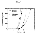
- the obtained organic photoelectric devices were measured for luminance using a luminance meter (Minolta Cs-000A) while increasing the voltage. The results are shown in FIG. 7 .
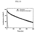
- Example 6 and Comparative Example 1 were compared about life-span by decreasing luminance depending on time with a reference to reference luminance of 1000 cd/m 2 . The results are shown in FIG. 10 .
- the organic photoelectric devices according to Examples 6 to 7 had remarkably better current density than the one according to Comparative Example 1 at the same voltage. A larger current density difference was shown at a higher high voltage.
- the organic photoelectric devices according to Examples 6 to 7 had remarkably better light emitting luminance than the one according to Comparative Example 1 at the same voltage. A larger light-emitting luminance difference was shown at a higher voltage.
- the organic photoelectric device according to Example 6 had greater than or equal to 20 times longer life-span than the one according to Comparative Example 1.
- Organic photoelectric devices including the compounds according to embodiments disclosed in the invention showed a low driving voltage and high luminous efficiency and thus an increased life span of a device, which was confirmed by device operation experiments.
Landscapes
- Chemical & Material Sciences (AREA)
- Engineering & Computer Science (AREA)
- Materials Engineering (AREA)
- Physics & Mathematics (AREA)
- Spectroscopy & Molecular Physics (AREA)
- Organic Chemistry (AREA)
- Optics & Photonics (AREA)
- Electroluminescent Light Sources (AREA)
- Photovoltaic Devices (AREA)
- Heterocyclic Carbon Compounds Containing A Hetero Ring Having Oxygen Or Sulfur (AREA)
- Plural Heterocyclic Compounds (AREA)
- Nitrogen Condensed Heterocyclic Rings (AREA)
Abstract
Description
- This application claims priority to and the benefit of Korean Patent Application No.
10-2009-0136182 - A compound for an organic photoelectric device being capable of providing an organic photoelectric device having excellent life-span, efficiency, electrochemical stability, and thermal stability, and an organic photoelectric device including the same are related.
- An organic photoelectric device is, in a broad sense, a device for transforming photo-energy to electrical energy, or conversely, a device for transforming electrical energy to photo-energy.
- An organic photoelectric device may be classified into two as follows in accordance with its driving principle. A organic photoelectric device is an electron device driven as follows: excitons are generated in an organic material layer by photons entering a device from an external light source; the excitons are separated into electrons and holes; and the electrons and holes are respectively transferred to different electrodes and used as a current source (a voltage source).
- A second organic photoelectric device is an electron device driven as follows: a voltage or a current is applied to at least two electrodes to inject holes and/or electrons into an organic material semiconductor positioned on an interface of the electrodes; and the injected electrons and holes drives the device.
- Examples of the organic photoelectric devices include an organic photoelectric device, an organic solar cell, an organic photo conductor drum, an organic transistor, and the like and require a hole injecting or transporting material, an electron injecting or transporting material, or a light emitting material.
- Particularly, an organic photoelectric device (an organic light emitting diode, OLED) has recently drawn attention due to an increasing demand for a flat panel display. In general, organic light emission refers to transformation of electrical energy to photo-energy.
- Such an organic photoelectric device transforms electrical energy into light by applying a current to an organic light emitting material and has a structure that a functional organic material layer is interposed between an anode and a cathode. The organic material layer includes a multi-layer respectively including different materials, for example, a hole injection layer (HIL), a hole transport layer (HTL), an emission layer, an electron transport layer (ETL), and an electron injection layer (EIL) in order to improve efficiency and stability of an organic photoelectric device.
- In such an organic photoelectric device, when a voltage is applied between an anode and a cathode, holes from the anode and electrons from the cathode are injected to an organic material layer and recombined to generate excitons having high energy. The generated excitons generate a light having a certain wavelength while shifting to a ground state.
- In 1987, Eastman Kodak, Inc. firstly developed an organic light emitting diode including a low molecular aromatic diamine and aluminum complex as an emission layer forming material (Applied Physics Letters. 51, 913, 1987). C.W Tang et al. firstly disclosed a practicable device as an organic light emitting diode in 1987 (Applied Physics Letters, 51 12, 913-915, 1987).
- According to the reference, the organic layer has a structure that a diamine derivative thin film (hole transport layer (HTL)) and a tris(8-hydroxy-quinolate)aluminum (Alq3) thin film are laminated.
- Recently, a phosphorescent light emitting material as well as a fluorescent light emitting material has become known to be used for a light emitting material of an organic light emitting diode (D. F. O'Brien et al., Applied Physics Letters, 74(3), 442-444, 1999; M. A. Baldo et al., Applied Physics letters, 75(1), 4-6, 1999). Such a phosphorescent material emits lights by transiting electrons from a ground state to an exited state, non-radiance transiting a singlet exciton to a triplet exciton through intersystem crossing, and transiting a triplet exciton to a ground state to emit a light.
- As described above, in an organic light emitting diode, an organic material layer includes a light emitting material and a charge transport material, for example, a hole injection material, a hole transport material, an electron transport material, an electron injection material, and so on.
- The light emitting material is classified as blue, green, and red light emitting materials according to emitted colors and yellow and orange light emitting materials to emit colors approaching natural colors.
- Since one light emitting material has a maximum light emitting wavelength shifted to a long wavelength and decrease color purity because of interactions among molecules or deteriorate device efficiency because of light emitting quenching effects, a host/dopant system may be used therewith in order to improve color purity and increase luminous efficiency and stability through energy transfer.
- In order to implement the aforementioned excellent performances of an organic photoelectric device, a material constituting an organic material layer, for example, a hole injection material, a hole transport material, a light emitting material, an electron transport material, an electron injection material, and a light emitting material such as a host and/or a dopant, should be first supported by a stable and efficient material. However, development of a material for an organic material layer for an organic light emitting diode has far not been satisfactory, and thus, there is a need for a novel material. This development of a novel material is also required for other organic photoelectric devices.
- A compound for an organic photoelectric device that may act as a electron injection and/or transport material and also, as a light emitting host along with an appropriate dopant is provided.
- An organic photoelectric device having excellent life span, efficiency, driving voltage, electrochemical stability, and thermal stability is provided.
- According to one aspect of the present invention, a compound for an organic photoelectric device represented by the following Chemical Formula 1 is provided.

- In
Chemical Formula 1, Ar1 is a substituted or unsubstituted C2 to C30 heteroaryl group, Ar2 to Ar5 are the same or different and independently a substituted or unsubstituted C6 to C30 aryl group, L1 and L2 are the same or different and independently a substituted or unsubstituted C6 to C30 arylene group, X1 to X3 are the same or different and independently a heteroatom or C-H, provided that at least one of X1 to X3 is a heteroatom, Y1 to Y3 are the same or different and independently a heteroatom or C-H, provided that at least one of Y1 to Y3 is a heteroatom. - According to one exemplary embodiment, Ar1 may be selected from the group consisting of a substituted or unsubstituted imidazolylene group, a substituted or unsubstituted thiazolylene group, a substituted or unsubstituted oxazolylene group, a substituted or unsubstituted oxadiazolylene group, a substituted or unsubstituted triazolylene group, a substituted or unsubstituted pyrimidinylene group, a substituted or unsubstituted pyridinylene group, a substituted or unsubstituted pyradazinylene group, a substituted or unsubstituted quinolinylene group, a substituted or unsubstituted isoquinolinylene group, a substituted or unsubstituted acridinylene group, a substituted or unsubstituted imidazopyridinylene group, and a substituted or unsubstituted imidazopyrimidinylene group.
- According to one exemplary embodiment, Ar1 may be a substituent selected from the group consisting of the following Chemical Formulae 2 to 7.


- In
Chemical Formulae 2 to 7, A1 to A6 are the same or different and independently a heteroatom or C-H, provided that at least one of A1 to A6 is a heteroatom, B1 to B5 are the same or different and are independently a heteroatom or C-H, provided that at least one of B1 to B5 is a heteroatom, C1 to C4 are the same or different and are independently a heteroatom or C-H, provided that at least one of C1 to C4 is a heteroatom, D1 to D4 are the same or different and are independently a heteroatom or C-H, provided that at least one of D1 to D4 is a heteroatom, E1 and E2 are the same or different and are independently a heteroatom or C-H, provided that at least one of E1 and E2 is a heteroatom, and R1 to R7 are the same or different and are independently selected from the group consisting of hydrogen, a substituted or unsubstituted C1 to C10 alkyl group, a substituted or unsubstituted C5 to C30 aryl group, and a substituted or unsubstituted C2 to C30 heteroaryl group. - According to one exemplary embodiment, Ar2 to Ar5 are the same or different and independently selected from the group consisting of a substituted or unsubstituted phenyl group, a substituted or unsubstituted naphthyl group, a substituted or unsubstituted anthracenyl group, a substituted or unsubstituted phenanthrenyl group, a substituted or unsubstituted pyrenyl group, a substituted or unsubstituted perylenyl group, and a substituted or unsubstituted chrysenyl group.
- According to one exemplary embodiment, L1 and L2 are the same or different and independently selected from the group consisting of a substituted or unsubstituted phenylene group, a substituted or unsubstituted naphthylene group, a substituted or unsubstituted anthracenylene group, a substituted or unsubstituted phenanthrenylene group, a substituted or unsubstituted pyrenylene group, a substituted or unsubstituted perylenylene group, and a substituted or unsubstituted chrysenylene group.
- According to another aspect of the present invention, provided is an organic photoelectric device that includes an anode, a cathode, and at least one or more organic thin layers between the anode and the cathode, wherein at least one of the organic thin layer includes the compound for an organic photoelectric device.
- The organic thin layer may be selected from the group consisting of an emission layer, a hole transport layer (HTL), a hole injection layer (HIL), an electron transport layer (ETL), an electron injection layer (EIL), a hole blocking layer, and a combination thereof.
- The compound for an organic photoelectric device may be included in an electron transport layer (ETL) or an electron injection layer (EIL).
- The compound for an organic photoelectric device may be included in an emission layer.
- The compound for an organic photoelectric device may be used as a phosphorescent or fluorescent host material in an emission layer.
- The compound for an organic photoelectric device may be used as a fluorescent blue dopant material in an emission layer.
- The organic photoelectric device may be selected from the group consisting of an organic light emitting diode, an organic solar cell, an organic transistor, an organic photo conductor drum, and an organic memory device.
- According to another aspect of the present invention, a display device including the organic photoelectric device is provided.
- An organic photoelectric device having life-span characteristic and high luminous efficiency at a low driving voltage may be provided due to excellent electrochemical and thermal stability.
-
-
FIGS. 1 to 5 are cross-sectional views showing organic photoelectric devices including compounds for an organic photoelectric device according to various embodiments of the present invention. -
FIG. 6 shows current density changes depending on voltage change according to Examples of the present invention and Comparative Example. -
FIG. 7 shows luminance changes depending on voltage change according to Examples of the present invention and Comparative Example. -
FIG. 8 shows luminous efficiency experimental data according to Examples of the present invention and Comparative Example. -
FIG. 9 shows electric power efficiency experimental data according to Examples of the present invention and Comparative Example. -
FIG. 10 shows life-span measurements and experimental data of the organic photoelectric devices according to Examples of the present invention and Comparative Example. -
100: organic photoelectric device 110: cathode 120: anode 105: organic thin layer 130: emission layer 140: hole transport layer (HTL) 150: electron transport layer (ETL) 160: electron injection layer (EIL) 170: hole injection layer (HIL) 230: emission layer + electron transport layer (ETL) - Exemplary embodiments of the present invention will hereinafter be described in detail. However, these embodiments are only exemplary, and the present invention is not limited thereto.
- Through the specification, the term "substituted" refers to one substituted with a C1 to C30 alkyl group, a C1 to C10 alkylsilyl group, a C3 to C30 cycloalkyl group, a C6 to C30 aryl group, a C1 to C10 alkoxy group, a fluoro group, a C1 to C10 trifluoroalkyl group such as a trifluoromethyl group, and the like, or a cyano group.
- Through the specification, the term "hetero" refers to one including 1 to 3 heteroatoms selected from the group consisting of N, O, S, and P and carbons in the rest thereof, in one ring.
- Through the specification, the term "a combination thereof" refers to at least two substituents bound to each other by a linker or at least two substituents fused to each other.
- Through the specification, when a definition is not otherwise provided, the term "alkyl" refers to an aliphatic hydrocarbon group. The alkyl may be a "saturated alkyl group" that does not include any alkene or alkyne. Alternatively, the alkyl may be an "unsaturated alkyl group" that includes at least one alkene or alkyne. The term "alkene" refers to a group in which at least two carbon atoms are bound in at least one carbon-carbon double bond, and the term "alkyne" refers to a group in which at least two carbon atoms are bound in at least one carbon-carbon triple bond. Regardless of being saturated or unsaturated, the alkyl may be branched, linear, or cyclic.
- The alkyl group may have 1 to 20 carbon atoms. The alkyl group may be a medium-sized alkyl having 1 to 10 carbon atoms. The alkyl group may be a lower alkyl having 1 to 6 carbon atoms.
- For example, a C1 to C4 alkyl may have 1 to 4 carbon atoms and may be selected from the group consisting of methyl, ethyl, propyl, iso-propyl, n-butyl, iso-butyl, sec-butyl, and t-butyl.
- Examples of an alkyl group may be selected from the group consisting of methyl, ethyl, propyl, isopropyl, butyl, isobutyl, t-butyl, pentyl, hexyl, ethenyl, propenyl, butenyl, cyclopropyl, cyclobutyl, cyclopentyl, cyclohexyl, or the like, which may be individually and independently substituted.
- The term "aryl" refers to an aryl group including a carbocyclic aryl (e.g., phenyl) having at least one ring having a covalent pi electron system. The term also refers to monocyclic or fused polycyclic (i.e., rings sharing adjacent pairs of carbon atoms) groups. In addition, this term also refers to a spiro compound having a contact point of one carbon.
- The term "heteroaryl" refers to a heterocyclic aryl group including a carbocyclic aryl (e.g., pyridine) having at least one ring having a covalent pi electron system. The term also refers to monocyclic or fusion ring polycyclic (i.e., groups sharing adjacent pairs of carbon atoms) groups. In addition, the term also refers to a spiro compound having a contact point of one carbon.
- According to one embodiment of the present invention, a compound for an organic photoelectric device may have a structure that a substituent represented by at least two "*-arylene group-heteroaryl groups" is combined with the core of a heteroarylene group. In the specification, "*" marks where a substituent is combined.
- In addition, the compound for an organic photoelectric device may have a core structure and include various substituents for the two substituents and thus, various energy band gaps and therefore, satisfy conditions required for an emission layer as well as an electron injection layer (EIL) and an electron transfer layer.
- When the compound having appropriate energy levels due to substituents is used for an organic photoelectric device, electron transfer capability may be reinforced and thus, excellent efficiency and driving voltage and excellent electrochemical and thermal stability may be improved resulting in improvement of life-span characteristics of the organic photoelectric device.
- According to one embodiment of the present invention, a compound for an organic photoelectric device represented by the following
Chemical Formula 1 is provided.
- In
Chemical Formula 1, Ar1 is a substituted or unsubstituted C2 to C30 heteroaryl group. For example, Ar1 is selected from the group consisting of a substituted or unsubstituted imidazolylene group, a substituted or unsubstituted thiazolylene group, a substituted or unsubstituted oxazolylene group, a substituted or unsubstituted oxadiazolylene group, a substituted or unsubstituted triazolylene group, a substituted or unsubstituted pyrimidinylene group, a substituted or unsubstituted pyridinylene group, a substituted or unsubstituted pyradazinylene group, a substituted or unsubstituted quinolinylene group, a substituted or unsubstituted isoquinolinylene group, a substituted or unsubstituted acridinylene group, a substituted or unsubstituted imidazopyridinylene group, and substituted or unsubstituted imidazopyrimidinylene group. - Specific examples of Ar1 may be a substituent selected from the group consisting of the following
Chemical Formulae 2 to 7.


- In
Chemical Formulae 2 to 7, A1 to A6 are the same or different and are independently a heteroatom or C-H, provided that at least one of A1 to A6 is a heteroatom, B1 to B5 are the same or different and are independently a heteroatom or C-H, provided that at least one of B1 to B5 is a heteroatom, C1 to C4 are the same or different and are independently a heteroatom or C-H, provided that at least one of C1 to C4 is a heteroatom, D1 to D4 are the same or different and are independently a heteroatom or C-H, provided that at least one of D1 to D4 is a heteroatom, E1 and E2 are the same or different and are independently a heteroatom or C-H, provided that at least one of E1 and E2 is a heteroatom, and R1 to R7 are the same or different and are independently selected from the group consisting of hydrogen, a substituted or unsubstituted C1 to C10 alkyl group, a substituted or unsubstituted C5 to C30 aryl group, and a substituted or unsubstituted C2 to C30 heteroaryl group. - The Ar1 is the core of the aforementioned heteroarylene group. As shown in
Chemical Formula 1, L1 and L2 may be combined with the core. - L1 and L2 are the same or different and independently a substituted or unsubstituted C6 to C30 arylene group. For example, L1 and L2 are the same or different and are independently selected from the group consisting of a substituted or unsubstituted phenylene group, a substituted or unsubstituted naphthylene group, a substituted or unsubstituted anthracenylene group, a substituted or unsubstituted phenanthrenylene group, a substituted or unsubstituted pyrenylene group, a substituted or unsubstituted perylenyl group, and a substituted or unsubstituted chrysenylene group.
- The L1 and L2 may be adjusted aboutπ-conjugation length to control light emission in a visible region. Accordingly, the compound may be usefully applied to an emission layer for an organic photoelectric device. However, when the number of carbons is out of the aforementioned range, the compound may not have sufficient effects on a device.
- When the compound is used to form an emission layer, a compound with the number of carbon of less than 6 may have inappropriate conjugation while a compound with the number of carbon more than 30 may inappropriately shift light-emitting colors toward an infrared region.
- In addition, even when the compound forms an electron transport layer (ETL), a compound having the number of carbon of less than 6 may have inappropriate conjugation, while a compound having the number of carbon of less than 30 may decrease a band gap and deteriorate capability of inhibiting a hole.
- As shown in
Chemical Formula 1, a heteroaryl group may be independently combined with the L1 and L2. - In
Chemical Formula 1, X1 to X3 are the same or different and independently a heteroatom or C-H, provided that at least one of X1 to X3 is a heteroatom, Y1 to Y3 are the same or different and are independently a heteroatom or C-H, provided that at least one of Y1 to Y3 is a heteroatom. - When the compound has a structure of combining the substituent, it may have excellent thermal stability due to hydrogen bonds of hetero atoms, improving life-span characteristics of an organic photoelectric device.
- In addition, Ar2 to Ar5, which are substituents combined with heteroaryl groups at the end, are the same or different and independently a substituted or unsubstituted C6 to C30 aryl group. For example, Ar2 to Ar5 are the same or different and are independently selected from the group consisting of a substituted or unsubstituted phenyl group, a substituted or unsubstituted naphthyl group, a substituted or unsubstituted anthracenyl group, a substituted or unsubstituted phenanthrenyl group, a substituted or unsubstituted pyrenyl group, a substituted or unsubstituted perylenyl group, a substituted or unsubstituted chrysenyl group.
- The Ar2 to Ar5 may adjust various electron transfer capabilities of a compound. In addition, crystallinity of the compound may be adjusted, accomplishing long life-span of a device.
- The compound for an organic photoelectric device may be represented by the following
Chemical Formulae 8 to 18. However, the present invention is not limited to the following compounds. The combination of the compounds may be represented by the followingcompounds 1 to 385.
- In
Chemical Formula 8, Ar2 to Ar5, X1 to X3, Y1 to Y3, L1, and L2 are the same as defined in the following Table 1.(Table 1) Compound Ar2 and Ar4 Ar3 and Ar5 L1 and L2 X1 and Y1 X2 and Y2 X3 and Y3 1 


N C C 2 C N C 3 C C N 4 N N C 5 N C N 6 C N N 7 N N N 8 


N C C 9 C N C 10 C C N 11 N N C 12 N C N 13 C N N 14 N N N 15 


N C C 16 C N C 17 C C N 18 N N C 19 N C N 20 C N N 21 N N N 22 


N C C 23 C N C 24 C C N 25 N N C 26 N C N 27 C N N 28 N N N 29 


N C C 30 C N C 31 C C N 32 N N C 33 N C N 34 C N N 35 N N N 
- In Chemical Formula 9, Ar2 to Ar5, X1 to X3, Y1 to Y3, L1, and L2 are the same as defined in the following Table 2.
(Table 2) Compound Ar2 and Ar4 Ar3 and Ar5 L1 and L2 X1 and Y1 X2 and Y2 X3 and Y3 36 


N C C 37 C N C 38 C C N 39 N N C 40 N C N 41 C N N 42 N N N 43 

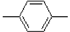
N C C 44 C N C 45 C C N 46 N N C 47 N C N 48 C N N 49 N N N 50 


N C C 51 C N C 52 C C N 53 N N C 54 N C N 55 C N N 56 N N N 57 


N C C 58 C N C 59 C C N 60 N N C 61 N C N 62 C N N 63 N N N 64 


N C C 65 C N C 66 C C N 67 N N C 68 N C N 69 C N N 70 N N N 

- In
Chemical Formula 10, Ar2 to Ar5, X1 to X3, Y1 to Y3, L1, and L2 are the same as defined in the following Table 3.(Table 3) Compound Ar2 and Ar4 Ar3 and Ar5 L1 and L2 X1 and Y1 X2 and Y2 X3 and Y3 71 
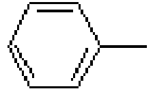

N C C 72 C N C 73 C C N 74 N N C 75 N C N 76 C N N 77 N N N 78 


N C C 79 C N C 80 C C N 81 N N C 82 N C N 83 C N N 84 N N N 85 


N C C 86 C N C 87 C C N 88 N N C 89 N C N 90 C N N 91 N N N 92 


N C C 93 C N C 94 C C N 95 N N C 96 N C N 97 C N N 98 N N N 99 


N C C 100 C N C 101 C C N 102 N N C 103 N C N 104 C N N 105 N N N 
- In Chemical Formula 11, Ar2 to Ar5, X1 to X3, Y1 to Y3, L1, and L2 are the same as defined in the following Table 4.
(Table 4) compound Ar2 and Ar4 Ar3 and Ar5 L1 and L2 X1 and Y1 X2 and Y2 X3 and Y3 106 


N C C 107 C N C 108 C C N 109 N N C 110 N C N 111 C N N 112 N N N 113 
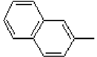

N C C 114 C N C 115 C C N 116 N N C 117 N C N 118 C N N 119 N N N 120 


N C C 121 C N C 122 C C N 123 N N C 124 N C N 125 C N N 126 N N N 127 


N C C 128 C N C 129 C C N 130 N N C 131 N C N 132 C N N 133 N N N 134 


N C C 135 C N C 136 C C N 137 N N C 138 N C N 139 C N N 140 N N N 
- In Chemical Formula 12, Ar2 to Ar5, X1 to X3, Y1 to Y3, L1, and L2 are the same as defined in the following Table 5.
(Table 5) Compound Ar2 and Ar4 Ar3 and Ar5 L1 and L2 X1 and Y1 X2 and Y2 X3 and Y3 141 


N C C 142 C N C 143 C C N 144 N N C 145 N C N 146 C N N 147 N N N 148 


N C C 149 C N C 150 C C N 151 N N C 152 N C N 153 C N N 154 N N N 155 


N C C 156 C N C 157 C C N 158 N N CC 159 N C N 160 C N N 161 N N N 162 


N C C 163 C N C 164 C C N 165 N N C 166 N C N 167 C N N 168 N N N 169 


N C C 170 C N C 171 C C N 172 N N C 173 N C N 174 C N N 175 N N N 

- In Chemical Formula 13, Ar2 to Ar5, X1 to X3, Y1 to Y3, L1, and L2 are the same as defined in the following Table 6.
(Table 6) Compound Ar2 and Ar4 Ar3 and Ar5 L1 and L2 X1 and Y1 X2 and Y2 X3 and Y3 176 


N C C 177 C N C 178 C C N 179 N N C 180 N C N 181 C N N 182 N N N 183 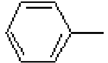


N C C 184 C N C 185 C C N 186 N N C 187 N C N 188 C N N 189 N N N 190 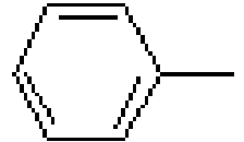


N C C 191 C N C 192 C C N 193 N N C 194 N C N 195 C N N 196 N N N 197 


N C C 198 C N C 199 C C N 200 N N C 201 N C N 202 C N N 203 N N N 204 


N C C 205 C N C 206 C C N 207 N N C 208 N C N 209 C N N 210 N N N 
- In Chemical Formula 14, Ar2 to Ar5, X1 to X3, Y1 to Y3, L1, and L2 are the same as defined in the following Table 7.
(Table 7) Compound Ar2 and Ar4 Ar3 and Ar5 L1 and L2 X1 and Y1 X2 and Y2 X3 and Y3 211 


N C C 212 C N C 213 C C N 214 N N C 215 N C N 216 C N N 217 N N N 218 


N C C 219 C N C 220 C C N 221 N N C 222 N C N 223 C N N 224 N N N 225 


N C C 226 C N C 227 C C N 228 N N C 229 N C N 230 C N N 231 N N N 232 


N C C 233 C N C 234 C C N 235 N N C 236 N C N 237 C N N 238 N N N 239 


N C C 240 C N C 241 C C N 242 N N C 243 N C N 244 C N N 245 N N N 
- In
Chemical Formula 15, Ar2 to Ar5, X1 to X3, Y1 to Y3, L1, and L2 are the same as defined in the following Table 8.(Table 8) Compound Ar2 and Ar4 Ar3 and Ar5 L1 and L2 X1 and Y1 X2 and Y2 X3 and Y3 246 


N C C 247 C N C 248 C C N 249 N N C 250 N C N 251 C N N 252 N N N 253 


N C C 254 C N C 255 C C N 256 N N C 257 N C N 258 C N N 259 N N N 260 


N C C 261 C N C 262 C C N 263 N N C 264 N C N 265 C N N 266 N N N 267 
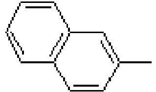

N C C 268 C N C 269 C C N 270 N N C 271 N C N 272 C N N 273 N N N 274 


N C C 275 C N C 276 C C N 277 N N C 278 N C N 279 C N N 280 N N N 

- In Chemical Formula 16, Ar2 to Ar5, X1 to X3, Y1 to Y3, L1, and L2 are the same as defined in the following Table 9.
(Table 9) Compound Ar2 and Ar4 Ar3 and Ar5 L1 and L2 X1 and Y1 X2 and Y2 X3 and Y3 281 


N C C 282 C N C 283 C C N 284 N N C 285 N C N 286 C N N 287 N N N 288 


N C C 289 C N C 290 C C N 291 N N C 292 N C N 293 C N N 294 N N N 295 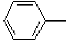


N C C 296 C N C 297 C C N 298 N N C 299 N C N 300 C N N 301 N N N 302 


N C C 303 C N C 304 C C N 305 N N C 306 N C N 307 C N N 308 N N N 309 


N C C 310 C N C 311 C C N 312 N N C 313 N C N 314 C N N 315 N N N 
- In Chemical Formula 17, Ar2 to Ar5, X1 to X3, Y1 to Y3, L1, and L2 are the same as defined in the following Table 10.
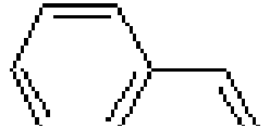
(Table 10) compound Ar2 and Ar4 Ar3 and Ar5 L1 and L2 X1 and Y1 X2 and Y2 X3 and Y3 316 


N C C 317 C N C 318 C C N 319 N N C 320 N C N 321 C N N 322 N N N 323 


N C C 324 C N C 325 C C N 326 N N C 327 N C N 328 C N N 329 N N N 330 


N C C 331 C N C 332 C C N 333 N N C 334 N C N 335 C N N 336 N N N 337 

N C C 338 C N C 339 C C N 340 N N C 341 N C N 342 C N N 343 N N N 344 


N C C 345 C N C 346 C C N 347 N N C 348 N C N 349 C N N 350 N N N 
- In Chemical Formula 18, Ar2 to Ar5, X1 to X3, Y1 to Y3, L1, and L2 are the same as defined in the following Table 11.
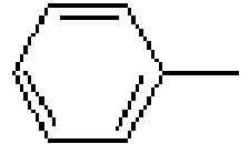
(Table 11) Compound Ar2 and Ar4 Ar3 and Ar5 L1 and L2 X1 and Y1 X2 and Y2 X3 and Y3 351 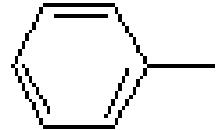

N C C 352 C N C 353 C C N 354 N N C 355 N C N 356 C N N 357 N N N 358 
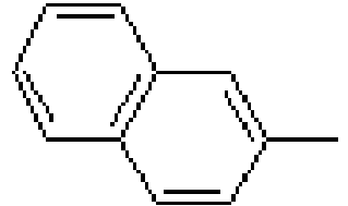

N C C 359 C N C 360 C C N 361 N N C 362 N C N 363 C N N 364 N N N 365 


N C C 366 C N C 367 C C N 368 N N C 369 N C N 370 C N N 371 N N N 372 


N C C 373 C N C 374 C C N 375 N N C 376 N C N 377 C N N 378 N N N 379 


N C C 380 C N C 381 C C N 382 N N C 383 N C N 384 C N N 385 N N N - The compound for an organic photoelectric device including the above compound has a glass transition temperature of higher than or equal to 110°C or and a thermal decomposition temperature of higher than or equal to 400°C, so as to improve thermal stability. Thereby, an organic photoelectric device having a high efficiency may be realized.
- The compound for an organic photoelectric device including the above compound may play a role for emitting light or injecting and/or transporting electrons, and it may act as a light emitting host together with a suitable dopant. The compound for an organic photoelectric device may be applied as a phosphorescent or fluorescent host material, a blue light emitting dopant material, or an electron transport material.
- Since the compound for an organic photoelectric device according to one embodiment is used for an organic thin layer, it may improve the life-span characteristic, efficiency characteristic, electrochemical stability, and thermal stability of an organic photoelectric device and decrease the driving voltage.
- Therefore, according to another embodiment, an organic photoelectric device is provided that includes the compound for an organic photoelectric device. The organic photoelectric device may include an organic photoelectric device, an organic solar cell, an organic transistor, an organic photosensitive drum, an organic memory device, or the like. For example, the compound for an organic photoelectric device according to one embodiment may be included in an electrode or an electrode buffer layer in the organic solar cell to improve the quantum efficiency, and it may be used as an electrode material for a gate electrode, a source-drain electrode, or the like in the organic transistor.
- Hereinafter, a detailed description relating to the organic photoelectric device will be provided.
- According to another embodiment of the present invention, the organic photoelectric device includes an anode, a cathode, and at least one organic thin layer interposed between the anode and the cathode, wherein the at least one organic thin layer may provide an organic photoelectric device including the compound for an organic photoelectric device according to one embodiment.
- The organic thin layer that may include the compound for an organic photoelectric device may include a layer selected from the group consisting of an emission layer, a hole transport layer (HTL), a hole injection layer (HIL), an electron transport layer (ETL), an electron injection layer (EIL), a hole blocking film, and a combination thereof. The at least one layer includes the compound for an organic photoelectric device according to one embodiment. Particularly, the electron transport layer (ETL) or the electron injection layer (EIL) may include the compound for an organic photoelectric device according to one embodiment. In addition, when the compound for an organic photoelectric device is included in the emission layer, the compound for an organic photoelectric device may be included as a phosphorescent or fluorescent host, and particularly, as a fluorescent blue dopant material.
-
FIGS. 1 to 5 are cross-sectional views showing an organic photoelectric device including the compound for an organic photoelectric device according to one embodiment of the present invention. - Referring to
FIGS. 1 to 5 , organicphotoelectric devices thin layer 105 interposed between ananode 120 and acathode 110. - The
anode 120 includes an anode material laving a large work function to help hole injection into an organic thin layer. The anode material includes: a metal such as nickel, platinum, vanadium, chromium, copper, zinc, and gold, or alloys thereof; a metal oxide such as zinc oxide, indium oxide, indium tin oxide (ITO), and indium zinc oxide (IZO); a combined metal and oxide such as ZnO:Al or SnO2:Sb; or a conductive polymer such as poly(3-methylthiophene), poly[3,4-(ethylene-1,2-dioxy)thiophene] (PEDT), polypyrrole, and polyaniline, but is not limited thereto. It is preferable to include a transparent electrode including indium tin oxide (ITO) as an anode. - The
cathode 110 includes a cathode material having a small work function to help electron injection into an organic thin layer. The cathode material includes: a metal such as magnesium, calcium, sodium, potassium, titanium, indium, yttrium, lithium, gadolinium, aluminum, silver, tin, and lead, or alloys thereof; or a multi-layered material such as LiF/Al, Liq/Al, LiO2/Al, LiF/Ca, LiF/Al, and BaF2/Ca, but is not limited thereto. It is preferable to include a metal electrode including aluminum as a cathode. - Referring to
FIG. 1 , the organicphotoelectric device 100 includes an organicthin layer 105 including only anemission layer 130. - Referring to
FIG. 2 , a double-layered organicphotoelectric device 200 includes an organicthin layer 105 including anemission layer 230 including an electron transport layer (ETL), and a hole transport layer (HTL) 140. As shown inFIG. 2 , the organicthin layer 105 includes a double layer of theemission layer 230 and hole transport layer (HTL) 140. Referring toFIG. 2 , a double-layered organicphotoelectric device 200 includes an organicthin layer 105 including anemission layer 230 including an electron transport layer (ETL), and a hole transport layer (HTL) 140. - Referring to
FIG. 3 , a three-layered organicphotoelectric device 300 includes an organicthin layer 105 including an electron transport layer (ETL) 150, anemission layer 130, and a hole transport layer (HTL) 140. Theemission layer 130 is independently installed, and layers having an excellent electron transporting property or an excellent hole transporting property are separately stacked. - As shown in
FIG. 4 , a four-layered organicphotoelectric device 400 includes an organicthin layer 105 including an electron injection layer (EIL) 160, anemission layer 130, a hole transport layer (HTL) 140, and a hole injection layer (HIL) 170 for binding with the cathode of ITO. - As shown in
FIG. 5 , a five layered organicphotoelectric device 500 includes an organicthin layer 105 including an electron transport layer (ETL) 150, anemission layer 130, a hole transport layer (HTL) 140, and a hole injection layer (HIL) 170, and further includes an electron injection layer (EIL) 160 to achieve a low voltage. - In
FIGS. 1 to 5 , the organicthin layer 105 including at least one selected from the group consisting of an electron transport layer (ETL) 150, an electron injection layer (EIL) 160, anemission layer - Furthermore, when the compound for an organic photoelectric device is included in the emission layers 130 and 230, the material for the organic photoelectric device may be included as a phosphorescent or fluorescent host or a fluorescent blue dopant.
- The organic photoelectric device may be fabricated by: forming an anode on a substrate; forming an organic thin layer in accordance with a dry coating method such as evaporation, sputtering, plasma plating, and ion plating or a wet coating method such as spin coating, dipping, and flow coating; and providing a cathode thereon.
- Another embodiment of the present invention provides a display device including the organic photoelectric device according to the above embodiment.
- Hereinafter, the embodiments are illustrated in more detail with reference to examples. However, the following are exemplary embodiments and are not limiting.
- The compound 246 as an example of the present invention was synthesized according to
Reaction Scheme 1.
- g (25 mmol) of 2,4-dichloro-6-(naphthalen-7-yl)pyrimidine, 24.3 g (56mmol) of 4-(4-(4,4,5,5-tetramethyl-1,3,2-dioxaborolan-2-yl)phenyl)-2,6-diphenyl pyridine, and 1.5g (1.3mmol) of tetrakis-(triphenylphosphine)palladium were suspended in a mixed solvent of 210 ml of tetrahydrofuran and 140 mL of toluene, and a solution prepared by dissolving 14.1g (100mmol) of potassium carbonate in 140mL of water was added thereto. The mixture was heated and refluxed for 12 hours. The liquid reactant was separated into two layers, and the organic layer thereof was cleaned with a sodium chloride saturated aqueous solution dried with anhydrous sodium sulfate. The organic solvent therein was distilled and removed under a reduced pressure, and the residue was recrystallized with toluene. Then, the precipitate was separated with a filter and cleaned with toluene, obtaining 16.7g of a compound (yield: 80.3%).
- (Calculation value : 816.99 / Measurement value : MS[M+1] 816)
- The compound 248 as an example of the present invention was synthesized according to the following
Reaction Scheme 2.
- 100 g (360 mmol) of 4-bromophenacyl bromide was slowly put into 1000 mL of pyridine, and the mixture was agitated at room temperature for 1 hour. The precipitated solid was filtered and cleaned with diethyl ether, obtaining 127.4 g of an intermediate product A (yield : 99 %).
- 185.2g (86.4 mmol) of the intermediate product A, 90 g (43.2 mmol) of trans chalcone, and 333 g (432 mmol) of ammonium acetate was suspended in 1200 mL of methanol, and the mixture was heated and refluxed for 12 hours. After cooling down the reactant, the precipitated solid was filtered and clean with methanol, obtaining 88.4 g of an intermediate product (B) (yield: 53 %).
- 130 g (337 mmol) of the intermediate product (B), 102.7 g (404.4 mmol) of bis(pinacolato)diboron, 6.9 g (8.4 mmol) of [1,1'-bis(diphenylphosphino)ferrocene]dichloropalladium (II), and 99.2 g (1011 mmol) of potassium acetate were suspended in 650 mL of dimethylformamide. The suspended reactant was agitated at 80°C for 12 hours. After cooling the reactant, the reactant was poured in distilled water to precipitate a solid. The solid was filtered and separated. The filtered solid was recrystallized with ethylacetate/hexane, obtaining 88.4 g of an intermediate product (C) (yield: 53%).
- 2.5 g (9.1 mmol) of 2,4-dichloro-6-(naphthalen-7-yl)pyrimidine, 8.7 g (20 mmol) of the intermediate product (C), and 0.5 g (0.5 mmol) of tetrakis-(triphenylphosphine)palladium were suspended in a mixed solvent of 75 mL of tetrahydrofuran and 50 mL of toluene, and a solution prepared by dissolving 5g (36.4 mmol) of potassium carbonate in 140 mL of water was added thereto. The mixture was heated and refluxed for 12 hours. The liquid reactant was separated into two layers, and the organic layer thereof was cleaned with a sodium chloride saturated aqueous solution and dried with anhydrous sodium sulfate. Then, an organic solvent therein was removed under a reduced pressure, and its residue was recrystallized for precipitation with toluene. The precipitate was filtered and cleaned with toluene, obtaining 6.2g of a compound (yield: 83.5%).
- (Calculation value: 816.99 / Measurement value: MS[M+1] 816)
- The compound 283 as an exampleof the present invention was synthesized according to the following Reaction Scheme 3.

- 24.9 g (100 mmol) of 2-bromo acetyl naphthalene and 25.2 g (100 ml) of 2-amino-3,5-dibromopyridine were suspended in 300 mL of ethanol. The suspension solution was heated and refluxed for 12 hours. After cooling down the reactant, the precipitated solid was filtered and cleaned with ethanol, obtaining 26.8 g of an intermediate product (D) (yield : 66 %).
- 3.5 g (8.7 mmol) of the intermediate product (D), 9.4 g (21.7 mmol) of the compound (C), and 0.5g (0.44 mmol) of tetrakis-(triphenylphosphine)palladium were suspended in 400 mL of tetrahydrofuran, and a solution prepared by dissolving 4.8 g (34.8 mmol) of potassium carbonate in 200 mL of water. The mixture was heated and refluxed for 12 hours. The liquid reactant was separated into two layers, and an organic layer thereof was cleaned with a sodium chloride saturated aqueous solution and dried with anhydrous sodium sulfate. Then, an organic solvent was distilled and removed under a reduced pressure, and its residue was recrystallized with tetrahydrofuran/methanol. The precipitate was filtered and separated and then, cleaned with methanol, obtaining 6.1g of a compound (yield: 82%).
- (Calculation value: 855.03 / Measurement value: MS[M+1] 855)
- The compound 318 as an exampleof the present invention was synthesized according to the following Reaction Scheme 4.


- 50 mL (451 mmol) of ethylbromoacetate was slowly put into 700 mL of pyridine. The mixture was agitated at room temperature for 2 hours. The precipitated solid therein was filtered and separated and cleaned with diethyl ether, obtaining 105 g of an intermediate product (E) (yield : 94 %).
- 42.5 g (172.9 mmol) of the intermediate product (E), 30 g (144 mmol) of transchalcone, and 111 g (1440 mmol) of ammonium acetate were suspended in 600 mL of methanol, and the mixture was heated and refluxed for 12 hours. After cooling down the reactant, the precipitated solid therein was filtered and separated and cleaned with methanol, obtaining 831.2 g of an intermediate product (F) (yield : 87 %).
- 20 g (80.9 mmol) of the intermediate product (F) and 25 g (87.2 mmol) of phosphoric acid tribromide were agitated together at 130°C for 2 hours. The liquid reactant was cooled down to room temperature, and water was poured for neutralization thereto. A solid produced therein was filtered. The obtained solid was cleaned with methanol, obtaining 17.3 g of an intermediate product (G) (yield : 68%).
- 50 g (180 mmol) of 4-bromophenacyl bromide and 20.3 g (220 ml) of 2-aminopyridine were suspended in 300 mL of ethanol. The suspension reactant was heated and refluxed for 12 hours. After cooling down the reactant , the precipitated solid produced therein was filtered and separated and cleaned with ethanol, obtaining 36.6 g of an intermediate product (H) (yield : 74 %).
- 27.3 g (100 mmol) of the intermediate product (H), 30.5 g (120 mmol) of bis(pinacolato)diboron, 0.82g (1mmol) of [1,1'-bis(diphenylphosphino)ferrocene]dichloropalladium (II), and 29.4g (300 mmol) of potassium acetate were suspended in 250 mL of dimethylformamide and agitated together at 80°C for 12 hours. After cooling down the reaction solution, it was poured down to distilled water for precipitation. The precipitated solid was filtered and separated. The filtered solid was recrystallized with ethylacetate/hexane, obtaining 22.6 g of an intermediate product (I) (yield : 70 %).
- 9.1 g (25.8 mmol) of the intermediate product (I), 8 g (21.7 mmol) of the compound (G), and 0.9 g (0.8 mmol) of tetrakis-(triphenylphosphine)palladium were suspended in 200 mL of tetrahydrofuran, and a solution prepared by dissolving 7.1 g (51.6 mmol) of potassium carbonate in 100 mL of water. The mixture was heated and refluxed for 12 hours. The liquid reactant was separated into two layers. The organic layer therein was cleaned with a sodium chloride saturated aqueous solution and dried with anhydrous sodium sulfate. Then, an organic solvent therein was distilled and removed under a reduced pressure, and its residue was separated with a silica gel column, obtaining 3.35g of a compound (J) (yield: 30%).
- 3.3 g (7.8 mmol) of the intermediate product (J) and 2.1 g (9.4 mmol) of N-iodosuccinimide were dissolved in 150 mL of tetrahydrofuran, and the solution was agitated at 50°C for 12 hours. After cooling down the reactant, its solvent was distilled under a reduced pressure. The obtained solid was dissolved in dichloromethane, and the solution was reprecipitated in methanol and filtered, obtaining 4.3 g of a compound (K) (yield: 100 %).
- 4.3 g (7.8 mmol) of the intermediate product (K), 4.1 g (9.4 mmol) of the compound (C), and 0.27 g (0.23 mmol) of tetrakis-(triphenylphosphine)palladium were suspended in 400 mL of tetrahydrofuran, and a solution prepared by dissolving 2.2 g (17.2 mmol) of potassium carbonate in 200 mL of water was added thereto. The mixture was heated and refluxed for 12 hours. The liquid reactant was separated into two layers, and the organic layer therein was cleaned with a sodium chloride saturated aqueous solution and dried with anhydrous sodium sulfate. Then, an organic solvent therein was distilled and removed under a reduced pressure, and its residue was separated with a silica gel column, obtaining 5.36 g of a compound (yield: 93%).
- (Calculation value: 728.88 / Measurement value: MS[M+1] 728)
- The compound 177 as an example of the present invention was synthesized according to the following
Reaction Scheme 5.
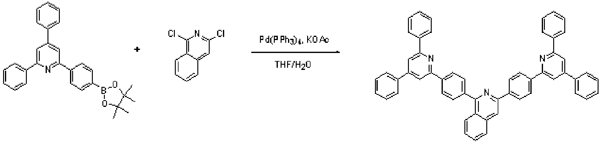
- 3 g (15.1 mmol) of 1,3-dichloroisoquinoline, 16.4 g (37.8 mmol) of the compound (C), and 0.9 g (0.76 mmol) of tetrakis-(triphenylphosphine)palladium were suspended in 180 mL of tetrahydrofuran, and a solution prepared by dissolving 8.3 g (60.4 mmol) of potassium carbonate in 90 mL of water was added thereto. The mixture was heated and refluxed for 12 hours. The liquid reactant was separated into two layers, and an organic layer therein was cleaned with a sodium chloride-saturated aqueous solution and dried with anhydrous sodium sulfate. Then, an organic solvent therein was distilled under a reduced pressure, and its residue was recrystallized with chlorobenzene, obtaining 5.4g of a compound (yield: 48%).
- (Calculation value: 739.90 / Measurement value: MS[M+1] 739)
- A glass transition temperature and a thermal decomposition temperature of the synthesized materials were measured using DSC and TGA.
- An organic photoelectric device was fabricated using 1000 A-thick ITO as an anode and 1000 A-thick aluminum (Al) as a cathode.
- In particular, the anode was prepared cutting an ITO glass substrate having a sheet resistance of 15 Ω/cm2 into a size of 50 mm x 50 mm x 0.7 mm and cleaning it in acetone, isopropylalcohol, and pure water, respectively for 5 minutes and with UV ozone for 30 minutes.
- Next, N1,N1'-(biphenyl-4,4'-diyl)bis(N1-(naphthalen-2-yl)-N4,N4-diphenylbenzene-1,4-diamine) was deposited to be 65 nm thick as a hole injection layer (HIL) on the glass substrate, and N,N'-di(1-naphthyl)-N,N'-diphenylbenzidine was deposited to be 40 nm thick as a hole transport layer (HTL).
- Then, 5% of N,N,N',N'-tetrakis(3,4-dimethylphenyl)chrysene-6,12-diamine and 95 % of 9-(3-(naphthalen-1-yl)phenyl)-10-(naphthalen-2-yl)anthracene were deposited to be 25 nm thick as an emission layer on the hole transport layer (HTL).
- Then, the compound according to Example 1 was deposited to be 30 nm thick on the emission layer as an electron transport layer (ETL).
- On the electron transport layer (ETL), Liq was vacuum-deposited to be 0.5 nm thick on the electron injection layer (EIL), and Al was vacuum-deposited to be 100 nm thick, forming a Liq/Al electrode.
- An organic photoelectric device was fabricated according to the same method as Example 6 except for using the compound according to Example 2 instead of the compound according to Example 1 to form an electron transport layer (ETL).
- An organic photoelectric device was fabricated according to the same method as Example 6 except for using the compound according to Example 4 instead of the compound according to Example 1 to form an electron transport layer (ETL).
- An organic photoelectric device was fabricated according to the same method as Example 6 except for using 35 nm-thick tris(8-hydroxy quinolato)aluminum (Alq3) instead of the compound according to Example 1 to form an electron transport layer (ETL).
- Each of the obtained organic photoelectric devices according to Examples 6 to 8 and Comparative Example 1 was measured for luminance change, current density change depending upon the voltage, and luminous efficiency. The specific method was as follows.
- The obtained organic photoelectric devices were measured for current values flowing in the unit devices while increasing the voltages using a current-voltage meter (Keithley 2400), and the measured current values were divided by an area to provide the results. The results are shown in
FIG. 6 . - The obtained organic photoelectric devices were measured for luminance using a luminance meter (Minolta Cs-000A) while increasing the voltage. The results are shown in
FIG. 7 . - Current efficiency and electric power efficiency were calculated by using luminance and current density from 1) and 2) and voltage. The results are shown in
FIGS. 8 and9 , and Table 12. - The organic photoelectric devices according to Example 6 and Comparative Example 1 were compared about life-span by decreasing luminance depending on time with a reference to reference luminance of 1000 cd/m2. The results are shown in
FIG. 10 . - As shown in
FIG. 6 , the organic photoelectric devices according to Examples 6 to 7 had remarkably better current density than the one according to Comparative Example 1 at the same voltage. A larger current density difference was shown at a higher high voltage. - In addition, as shown in
FIG. 7 , the organic photoelectric devices according to Examples 6 to 7 had remarkably better light emitting luminance than the one according to Comparative Example 1 at the same voltage. A larger light-emitting luminance difference was shown at a higher voltage. - As shown in
FIGS. 8 and9 and the following Table 12, the organic photoelectric devices according to Examples 6 and 7 had remarkably excellent luminous efficiency and electric power efficiency compared with the one according to Comparative Example 1.(Table 12) Luminance at 500 cd/m2 Driving voltage (V) Luminous efficiency (cd/A) Electric power efficiency (Im/W) Example 6 4.3 9.1 6.7 Example 7 4 5.85 4.59 Example 8 5.8 4.39 2.38 Comparative Example 1 6.6 3.58 1.70 - As shown in
FIG. 10 , the organic photoelectric device according to Example 6 had greater than or equal to 20 times longer life-span than the one according to Comparative Example 1. - Organic photoelectric devices including the compounds according to embodiments disclosed in the invention showed a low driving voltage and high luminous efficiency and thus an increased life span of a device, which was confirmed by device operation experiments.
- While this invention has been described in connection with what is presently considered to be practical exemplary embodiments, it is to be understood that the invention is not limited to the disclosed embodiments, but, on the contrary, is intended to cover various modifications and equivalent arrangements included within the spirit and scope of the appended claims. Therefore, the aforementioned embodiments should be understood to be exemplary but not limiting the present invention in any way.
Claims (13)
- A compound for an organic photoelectric device represented by the following Chemical Formula 1:

Ar1 is a substituted or unsubstituted C2 to C30 heteroaryl group,
Ar2 to Ar5 are the same or different and independently a substituted or unsubstituted C6 to C30 aryl group,
L1 and L2 are the same or different and independently a substituted or unsubstituted C6 to C30 arylene group,
X1 to X3 are the same or different and independently a heteroatom or C-H, provided that at least one of X1 to X3 is a heteroatom, and
Y1 to Y3 are the same or different and independently a heteroatom or C-H, provided that at least one of Y1 to Y3 is a heteroatom. - The compound of claim 1, wherein Ar1 is selected from the group consisting of a substituted or unsubstituted imidazolylene group, a substituted or unsubstituted thiazolylene group, a substituted or unsubstituted oxazolylene group, a substituted or unsubstituted oxadiazolylene group, a substituted or unsubstituted triazolylene group, a substituted or unsubstituted pyrimidinylene group, a substituted or unsubstituted pyridinylene group, a substituted or unsubstituted pyradazinylene group, a substituted or unsubstituted quinolinylene group, a substituted or unsubstituted isoquinolinylene group, a substituted or unsubstituted acridinylene group, a substituted or unsubstituted imidazopyridinylene group, and a substituted or unsubstituted imidazopyrimidinylene group.
- The compound of claim 1, wherein Ar1 is a substituent selected from the group consisting of the following Chemical Formulae 2 to 7:

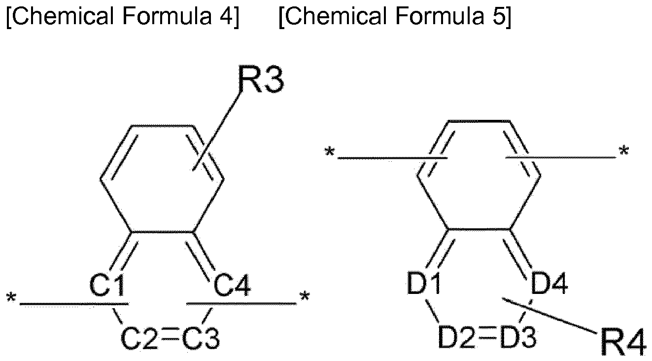

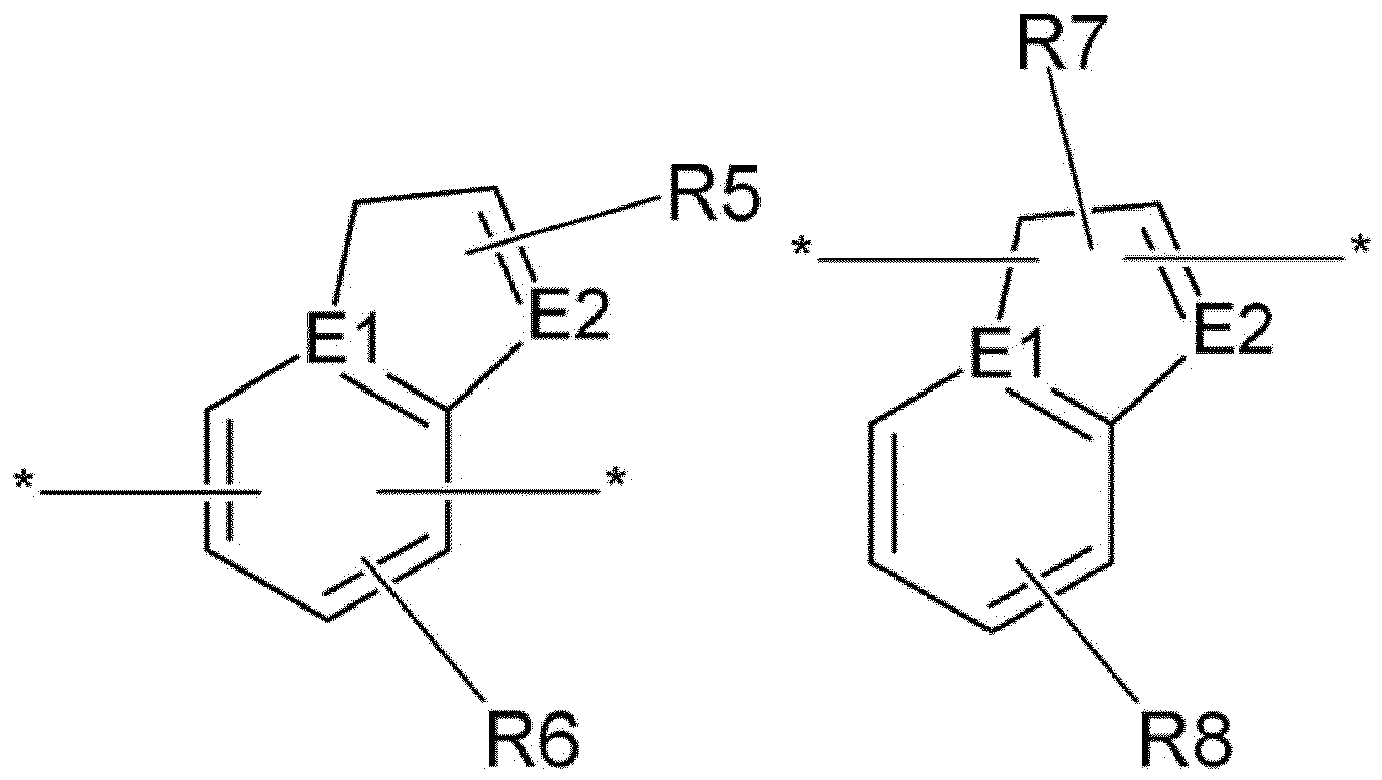
A1 to A6 are the same or different and independently a heteroatom or C-H, provided that at least one of A1 to A6 is a heteroatom,
B1 to B5 are the same or different and independently a heteroatom or C-H, provided that at least one of B1 to B5 is a heteroatom,
C1 to C4 are the same or different and independently a heteroatom or C-H, provided that at least one of C1 to C4 is a heteroatom,
D1 to D4 are the same or different and independently a heteroatom or C-H, provided that at least one of D1 to D4 is a heteroatom,
E1 and E2 are the same or different and independently a heteroatom or C-H, provided that at least one of E1 and E2 is a heteroatom, and
R1 to R7 are the same or different and independently selected from the group consisting of hydrogen, a substituted or unsubstituted C1 to C10 alkyl group, a substituted or unsubstituted C5 to C30 aryl group, and a substituted or unsubstituted C2 to C30 heteroaryl group. - The compound of claim 1, wherein Ar2 to Ar5 are the same or different and are independently selected from the group consisting of a substituted or unsubstituted phenyl group, a substituted or unsubstituted naphthyl group, a substituted or unsubstituted anthracenyl group, a substituted or unsubstituted phenanthrenyl group, a substituted or unsubstituted pyrenyl group, a substituted or unsubstituted perylenyl group, a substituted or unsubstituted chrysenyl group.
- The compound of claim 1, wherein L1 and L2 are the same or different and are independently selected from the group consisting of a substituted or unsubstituted phenylene group, a substituted or unsubstituted naphthylene group, a substituted or unsubstituted anthracenylene group, a substituted or unsubstituted phenanthrenylene group, a substituted or unsubstituted pyrenylene group, a substituted or unsubstituted perylenylene group, and a substituted or unsubstituted chrysenylene group.
- An organic photoelectric device comprising
an anode, a cathode, and at least one or more organic thin layers between the anode and the cathode,
wherein at least one of the organic thin layer comprises the compound for an organic photoelectric device according to one of claims 1 to 5. - The organic photoelectric device of claim 6, wherein the organic thin layer is selected from the group consisting of an emission layer, a hole transport layer (HTL), a hole injection layer (HIL), an electron transport layer (ETL), an electron injection layer (EIL), a hole blocking layer, and a combination thereof.
- The organic photoelectric device of claim 6, wherein the compound for an organic photoelectric device is included in an electron transport layer (ETL) or an electron injection layer (EIL).
- The organic photoelectric device of claim 6, wherein the compound for an organic photoelectric device is included in an emission layer.
- The organic photoelectric device of claim 6, wherein the compound for an organic photoelectric device is used as a phosphorescent or fluorescent host material in an emission layer.
- The organic photoelectric device of claim 6, wherein the compound for an organic photoelectric device is used as a fluorescent blue dopant material in an emission layer.
- The organic photoelectric device of claim 6, wherein the organic photoelectric device is selected from the group consisting of an organic light emitting diode, an organic solar cell, an organic transistor, an organic photo conductor drum, and an organic memory device.
- A display device including the organic photoelectric device according to claim 6.
Applications Claiming Priority (2)
| Application Number | Priority Date | Filing Date | Title |
|---|---|---|---|
| KR1020090136182A KR20110079197A (en) | 2009-12-31 | 2009-12-31 | Compound for organic photoelectric device and organic photoelectric device comprising same |
| PCT/KR2010/007763 WO2011081290A2 (en) | 2009-12-31 | 2010-11-04 | Compound for organic photoelectric device and organic photoelectric device including the compound |
Publications (1)
| Publication Number | Publication Date |
|---|---|
| EP2520632A2 true EP2520632A2 (en) | 2012-11-07 |
Family
ID=44226929
Family Applications (1)
| Application Number | Title | Priority Date | Filing Date |
|---|---|---|---|
| EP10841123A Withdrawn EP2520632A2 (en) | 2009-12-31 | 2010-11-04 | Compound for organic photoelectric device and organic photoelectric device including the compound |
Country Status (5)
| Country | Link |
|---|---|
| US (1) | US20120273771A1 (en) |
| EP (1) | EP2520632A2 (en) |
| JP (1) | JP2013516405A (en) |
| KR (1) | KR20110079197A (en) |
| WO (1) | WO2011081290A2 (en) |
Cited By (1)
| Publication number | Priority date | Publication date | Assignee | Title |
|---|---|---|---|---|
| CN114478416A (en) * | 2022-02-14 | 2022-05-13 | 季华恒烨(佛山)电子材料有限公司 | Pyrene-triazine-based organic compound, organic electroluminescent composition and organic electroluminescent device |
Families Citing this family (12)
| Publication number | Priority date | Publication date | Assignee | Title |
|---|---|---|---|---|
| KR101474800B1 (en) * | 2011-08-19 | 2014-12-19 | 제일모직 주식회사 | Compound for organic OPTOELECTRONIC device, ORGANIC LIGHT EMITTING DIODE INCLUDING THE SAME and DISPLAY INCLUDING THE organic LIGHT EMITTING DIODE |
| US9847501B2 (en) | 2011-11-22 | 2017-12-19 | Idemitsu Kosan Co., Ltd. | Aromatic heterocyclic derivative, material for organic electroluminescent element, and organic electroluminescent element |
| JP2015524610A (en) | 2012-07-04 | 2015-08-24 | サムスン エスディアイ カンパニー,リミテッド | Composition for organic light emitting device, organic light emitting layer containing the same, and organic light emitting device |
| WO2014010823A1 (en) | 2012-07-13 | 2014-01-16 | 주식회사 엘지화학 | Heterocyclic compound and organic electronic element containing same |
| KR101499356B1 (en) | 2013-06-28 | 2015-03-05 | 주식회사 엘지화학 | Hetero-cyclic compound and organic light emitting device comprising the same |
| KR101644700B1 (en) * | 2013-09-24 | 2016-08-01 | 주식회사 엘지화학 | Hetero-cyclic compound and organic light emitting device comprising the same |
| KR101602533B1 (en) * | 2013-09-30 | 2016-03-10 | 주식회사 엘지화학 | Hetero-cyclic compound and organic light emitting device comprising the same |
| EP3040335B1 (en) | 2013-11-13 | 2019-04-03 | Idemitsu Kosan Co., Ltd | Compound, organic electroluminescent element, and electronic device |
| EP3156402B1 (en) * | 2014-06-11 | 2021-11-10 | Hodogaya Chemical Co., Ltd. | Pyrimidine derivative and organic electroluminescent element |
| WO2016084962A1 (en) | 2014-11-28 | 2016-06-02 | 出光興産株式会社 | Compound, organic electroluminescence element material, organic electroluminescence element and electronic device |
| EP3515447A4 (en) * | 2016-09-26 | 2020-05-27 | Tufts University | NUCLEOSIDE URIDINE DERIVATIVES, COMPOSITIONS AND METHODS OF USE |
| KR102019923B1 (en) * | 2019-01-23 | 2019-09-11 | 솔브레인 주식회사 | Compound and organic light emitting device comprising the same |
Family Cites Families (6)
| Publication number | Priority date | Publication date | Assignee | Title |
|---|---|---|---|---|
| US6057048A (en) * | 1998-10-01 | 2000-05-02 | Xerox Corporation | Electroluminescent (EL) devices |
| DE10229370A1 (en) * | 2002-06-29 | 2004-01-15 | Covion Organic Semiconductors Gmbh | 2,1,3-benzothiadiazoles |
| KR100994083B1 (en) * | 2003-07-31 | 2010-11-12 | 미쓰비시 가가꾸 가부시키가이샤 | Compound, charge transport material and organic electroluminescent device |
| JP2009114068A (en) * | 2007-11-01 | 2009-05-28 | Canon Inc | Triphenylene compound and organic light emitting device using the same |
| KR100948853B1 (en) * | 2007-11-16 | 2010-03-22 | 삼성모바일디스플레이주식회사 | Heterocyclic compound and organic electroluminescent device using same |
| KR20090131958A (en) * | 2008-06-19 | 2009-12-30 | 제일모직주식회사 | Compound for organic photoelectric device and organic photoelectric device including same |
-
2009
- 2009-12-31 KR KR1020090136182A patent/KR20110079197A/en not_active Ceased
-
2010
- 2010-11-04 WO PCT/KR2010/007763 patent/WO2011081290A2/en not_active Ceased
- 2010-11-04 EP EP10841123A patent/EP2520632A2/en not_active Withdrawn
- 2010-11-04 JP JP2012546983A patent/JP2013516405A/en active Pending
-
2012
- 2012-06-29 US US13/537,952 patent/US20120273771A1/en not_active Abandoned
Non-Patent Citations (1)
| Title |
|---|
| See references of WO2011081290A2 * |
Cited By (2)
| Publication number | Priority date | Publication date | Assignee | Title |
|---|---|---|---|---|
| CN114478416A (en) * | 2022-02-14 | 2022-05-13 | 季华恒烨(佛山)电子材料有限公司 | Pyrene-triazine-based organic compound, organic electroluminescent composition and organic electroluminescent device |
| CN114478416B (en) * | 2022-02-14 | 2023-11-14 | 季华恒烨(佛山)电子材料有限公司 | Pyrene-triazine-based organic compound, organic electroluminescent composition and organic electroluminescent device |
Also Published As
| Publication number | Publication date |
|---|---|
| WO2011081290A9 (en) | 2012-09-20 |
| US20120273771A1 (en) | 2012-11-01 |
| WO2011081290A3 (en) | 2011-09-22 |
| WO2011081290A4 (en) | 2011-12-01 |
| KR20110079197A (en) | 2011-07-07 |
| WO2011081290A2 (en) | 2011-07-07 |
| JP2013516405A (en) | 2013-05-13 |
Similar Documents
| Publication | Publication Date | Title |
|---|---|---|
| EP2514798B1 (en) | Compound for organic photoelectric device and organic photoelectric device including same | |
| KR101387738B1 (en) | Compound for organic photoelectric device and organic photoelectric device including the same | |
| EP2842954B1 (en) | Compound for organic optoelectric device, organic light emitting device containing same, and display device containing said organic light emitting device | |
| EP3460024B1 (en) | Compound for an organic photoelectric device, and organic photoelectric device comprising same | |
| KR101297158B1 (en) | Compound for organic photoelectric device and organic photoelectric device including the same | |
| KR101233380B1 (en) | Novel compound for organic photoelectric device and organic photoelectric device including the same | |
| KR101508424B1 (en) | Hetero-cyclic compound and organic electronic device comprising the same | |
| US8697257B2 (en) | Compound for organic photoelectric device, organic photoelectric device including the same, and display device including the organic photoelectric device | |
| CN104245697B (en) | Nitrogen-containing heterocyclic compounds and organic electronic devices containing them | |
| KR101565200B1 (en) | New compound and organic light emitting device using the same | |
| KR101174090B1 (en) | Material for organic photoelectric device and organic photoelectric device including the same | |
| EP2508585B1 (en) | Compound for organic optoelectronic device, organic light emitting diode including the same, and display device including organic light emitting diode | |
| US20120273771A1 (en) | Compound for organic photoelectric device and organic photoelectric device including the same | |
| US20130200356A1 (en) | Compound for organic optoelectronic device, organic light emitting diode including the same and display including the organic light emitting diode | |
| US20130299794A1 (en) | Compound for organic optoelectronic device, organic light emitting diode including the same and display including the organic light emitting diode | |
| KR20140087647A (en) | Compound for organic optoelectronic device, organic light emitting diode including the same and display including the organic light emitting diode | |
| KR20140087996A (en) | Compound for organic optoelectronic device, organic light emitting diode including the same and display including the organic light emitting diode | |
| KR101897039B1 (en) | Organic compound and composition and organic optoelectric device and display device | |
| KR101497137B1 (en) | Compound for organic optoelectronic device, organic light emitting diode including the same and display including the organic light emitting diode | |
| EP2998380A1 (en) | Compound for organic optoelectric device, organic light-emitting diode including same, display device including organic light-emitting diode | |
| KR102092799B1 (en) | Organic compound and organic optoelectronic device and display device | |
| KR20190089763A (en) | Multicyclic compound and organic light emitting device comprising the same | |
| KR20140087648A (en) | Compound for organic optoelectronic device, organic light emitting diode including the same and display including the organic light emitting diode | |
| KR20140102024A (en) | Compound for organic optoelectronic device, organic light emitting diode including the same and display including the organic light emitting diode |
Legal Events
| Date | Code | Title | Description |
|---|---|---|---|
| PUAI | Public reference made under article 153(3) epc to a published international application that has entered the european phase |
Free format text: ORIGINAL CODE: 0009012 |
|
| 17P | Request for examination filed |
Effective date: 20120720 |
|
| AK | Designated contracting states |
Kind code of ref document: A2 Designated state(s): AL AT BE BG CH CY CZ DE DK EE ES FI FR GB GR HR HU IE IS IT LI LT LU LV MC MK MT NL NO PL PT RO RS SE SI SK SM TR |
|
| RIN1 | Information on inventor provided before grant (corrected) |
Inventor name: LEE, NAM-HEON Inventor name: CHAE, MI-YOUNG Inventor name: JUNG, HO-KUK Inventor name: KIM, NAM-SOO Inventor name: KANG, EUI-SU Inventor name: JUNG, SUNG-HYUN Inventor name: KANG, MYEONG-SOON Inventor name: IN, KYU-YEOL Inventor name: KANG, DONG-MIN |
|
| DAX | Request for extension of the european patent (deleted) | ||
| STAA | Information on the status of an ep patent application or granted ep patent |
Free format text: STATUS: THE APPLICATION HAS BEEN WITHDRAWN |
|
| 18W | Application withdrawn |
Effective date: 20130807 |