EP2520406A2 - Communications terminal and method of manufacturing the same - Google Patents
Communications terminal and method of manufacturing the same Download PDFInfo
- Publication number
- EP2520406A2 EP2520406A2 EP12275041A EP12275041A EP2520406A2 EP 2520406 A2 EP2520406 A2 EP 2520406A2 EP 12275041 A EP12275041 A EP 12275041A EP 12275041 A EP12275041 A EP 12275041A EP 2520406 A2 EP2520406 A2 EP 2520406A2
- Authority
- EP
- European Patent Office
- Prior art keywords
- communications terminal
- antenna pattern
- terminal
- antenna
- case
- Prior art date
- Legal status (The legal status is an assumption and is not a legal conclusion. Google has not performed a legal analysis and makes no representation as to the accuracy of the status listed.)
- Withdrawn
Links
- 238000004891 communication Methods 0.000 title claims abstract description 60
- 238000004519 manufacturing process Methods 0.000 title claims abstract description 17
- 238000001746 injection moulding Methods 0.000 claims abstract description 24
- 238000003780 insertion Methods 0.000 claims description 29
- 230000037431 insertion Effects 0.000 claims description 29
- 238000000034 method Methods 0.000 claims description 21
- 239000011347 resin Substances 0.000 claims description 12
- 229920005989 resin Polymers 0.000 claims description 12
- 239000000463 material Substances 0.000 claims description 7
- 230000008878 coupling Effects 0.000 claims description 6
- 238000010168 coupling process Methods 0.000 claims description 6
- 238000005859 coupling reaction Methods 0.000 claims description 6
- 230000000149 penetrating effect Effects 0.000 claims description 3
- 239000012790 adhesive layer Substances 0.000 description 6
- 229910052751 metal Inorganic materials 0.000 description 5
- 239000002184 metal Substances 0.000 description 5
- 239000000853 adhesive Substances 0.000 description 3
- 230000001070 adhesive effect Effects 0.000 description 3
- 239000010410 layer Substances 0.000 description 3
- 238000007747 plating Methods 0.000 description 3
- 230000008569 process Effects 0.000 description 3
- PXHVJJICTQNCMI-UHFFFAOYSA-N Nickel Chemical compound [Ni] PXHVJJICTQNCMI-UHFFFAOYSA-N 0.000 description 2
- 238000005516 engineering process Methods 0.000 description 2
- 238000012986 modification Methods 0.000 description 2
- 230000004048 modification Effects 0.000 description 2
- 238000003825 pressing Methods 0.000 description 2
- RYGMFSIKBFXOCR-UHFFFAOYSA-N Copper Chemical compound [Cu] RYGMFSIKBFXOCR-UHFFFAOYSA-N 0.000 description 1
- 239000004831 Hot glue Substances 0.000 description 1
- 229910052782 aluminium Inorganic materials 0.000 description 1
- XAGFODPZIPBFFR-UHFFFAOYSA-N aluminium Chemical compound [Al] XAGFODPZIPBFFR-UHFFFAOYSA-N 0.000 description 1
- 230000001413 cellular effect Effects 0.000 description 1
- 229910052802 copper Inorganic materials 0.000 description 1
- 239000010949 copper Substances 0.000 description 1
- 238000007429 general method Methods 0.000 description 1
- PCHJSUWPFVWCPO-UHFFFAOYSA-N gold Chemical compound [Au] PCHJSUWPFVWCPO-UHFFFAOYSA-N 0.000 description 1
- 229910052737 gold Inorganic materials 0.000 description 1
- 239000010931 gold Substances 0.000 description 1
- 238000002347 injection Methods 0.000 description 1
- 239000007924 injection Substances 0.000 description 1
- 238000009413 insulation Methods 0.000 description 1
- 239000007769 metal material Substances 0.000 description 1
- 239000012778 molding material Substances 0.000 description 1
- 238000000465 moulding Methods 0.000 description 1
- 229910052759 nickel Inorganic materials 0.000 description 1
- 238000007639 printing Methods 0.000 description 1
- 238000011160 research Methods 0.000 description 1
- 238000000926 separation method Methods 0.000 description 1
- 229910000679 solder Inorganic materials 0.000 description 1
- 238000004544 sputter deposition Methods 0.000 description 1
- 239000000758 substrate Substances 0.000 description 1
Images



Classifications
-
- H—ELECTRICITY
- H04—ELECTRIC COMMUNICATION TECHNIQUE
- H04B—TRANSMISSION
- H04B1/00—Details of transmission systems, not covered by a single one of groups H04B3/00 - H04B13/00; Details of transmission systems not characterised by the medium used for transmission
- H04B1/38—Transceivers, i.e. devices in which transmitter and receiver form a structural unit and in which at least one part is used for functions of transmitting and receiving
-
- H—ELECTRICITY
- H04—ELECTRIC COMMUNICATION TECHNIQUE
- H04M—TELEPHONIC COMMUNICATION
- H04M1/00—Substation equipment, e.g. for use by subscribers
- H04M1/02—Constructional features of telephone sets
- H04M1/0202—Portable telephone sets, e.g. cordless phones, mobile phones or bar type handsets
- H04M1/026—Details of the structure or mounting of specific components
-
- B—PERFORMING OPERATIONS; TRANSPORTING
- B29—WORKING OF PLASTICS; WORKING OF SUBSTANCES IN A PLASTIC STATE IN GENERAL
- B29C—SHAPING OR JOINING OF PLASTICS; SHAPING OF MATERIAL IN A PLASTIC STATE, NOT OTHERWISE PROVIDED FOR; AFTER-TREATMENT OF THE SHAPED PRODUCTS, e.g. REPAIRING
- B29C45/00—Injection moulding, i.e. forcing the required volume of moulding material through a nozzle into a closed mould; Apparatus therefor
- B29C45/14—Injection moulding, i.e. forcing the required volume of moulding material through a nozzle into a closed mould; Apparatus therefor incorporating preformed parts or layers, e.g. injection moulding around inserts or for coating articles
- B29C45/14639—Injection moulding, i.e. forcing the required volume of moulding material through a nozzle into a closed mould; Apparatus therefor incorporating preformed parts or layers, e.g. injection moulding around inserts or for coating articles for obtaining an insulating effect, e.g. for electrical components
-
- B—PERFORMING OPERATIONS; TRANSPORTING
- B29—WORKING OF PLASTICS; WORKING OF SUBSTANCES IN A PLASTIC STATE IN GENERAL
- B29C—SHAPING OR JOINING OF PLASTICS; SHAPING OF MATERIAL IN A PLASTIC STATE, NOT OTHERWISE PROVIDED FOR; AFTER-TREATMENT OF THE SHAPED PRODUCTS, e.g. REPAIRING
- B29C45/00—Injection moulding, i.e. forcing the required volume of moulding material through a nozzle into a closed mould; Apparatus therefor
- B29C45/16—Making multilayered or multicoloured articles
- B29C45/1671—Making multilayered or multicoloured articles with an insert
-
- H—ELECTRICITY
- H01—ELECTRIC ELEMENTS
- H01Q—ANTENNAS, i.e. RADIO AERIALS
- H01Q1/00—Details of, or arrangements associated with, antennas
- H01Q1/12—Supports; Mounting means
- H01Q1/22—Supports; Mounting means by structural association with other equipment or articles
- H01Q1/24—Supports; Mounting means by structural association with other equipment or articles with receiving set
-
- H—ELECTRICITY
- H01—ELECTRIC ELEMENTS
- H01Q—ANTENNAS, i.e. RADIO AERIALS
- H01Q1/00—Details of, or arrangements associated with, antennas
- H01Q1/12—Supports; Mounting means
- H01Q1/22—Supports; Mounting means by structural association with other equipment or articles
- H01Q1/24—Supports; Mounting means by structural association with other equipment or articles with receiving set
- H01Q1/241—Supports; Mounting means by structural association with other equipment or articles with receiving set used in mobile communications, e.g. GSM
- H01Q1/242—Supports; Mounting means by structural association with other equipment or articles with receiving set used in mobile communications, e.g. GSM specially adapted for hand-held use
- H01Q1/243—Supports; Mounting means by structural association with other equipment or articles with receiving set used in mobile communications, e.g. GSM specially adapted for hand-held use with built-in antennas
-
- H—ELECTRICITY
- H01—ELECTRIC ELEMENTS
- H01Q—ANTENNAS, i.e. RADIO AERIALS
- H01Q7/00—Loop antennas with a substantially uniform current distribution around the loop and having a directional radiation pattern in a plane perpendicular to the plane of the loop
-
- H—ELECTRICITY
- H04—ELECTRIC COMMUNICATION TECHNIQUE
- H04M—TELEPHONIC COMMUNICATION
- H04M1/00—Substation equipment, e.g. for use by subscribers
- H04M1/02—Constructional features of telephone sets
-
- B—PERFORMING OPERATIONS; TRANSPORTING
- B29—WORKING OF PLASTICS; WORKING OF SUBSTANCES IN A PLASTIC STATE IN GENERAL
- B29C—SHAPING OR JOINING OF PLASTICS; SHAPING OF MATERIAL IN A PLASTIC STATE, NOT OTHERWISE PROVIDED FOR; AFTER-TREATMENT OF THE SHAPED PRODUCTS, e.g. REPAIRING
- B29C45/00—Injection moulding, i.e. forcing the required volume of moulding material through a nozzle into a closed mould; Apparatus therefor
- B29C45/16—Making multilayered or multicoloured articles
- B29C45/1671—Making multilayered or multicoloured articles with an insert
- B29C2045/1673—Making multilayered or multicoloured articles with an insert injecting the first layer, then feeding the insert, then injecting the second layer
-
- B—PERFORMING OPERATIONS; TRANSPORTING
- B29—WORKING OF PLASTICS; WORKING OF SUBSTANCES IN A PLASTIC STATE IN GENERAL
- B29L—INDEXING SCHEME ASSOCIATED WITH SUBCLASS B29C, RELATING TO PARTICULAR ARTICLES
- B29L2031/00—Other particular articles
- B29L2031/34—Electrical apparatus, e.g. sparking plugs or parts thereof
- B29L2031/3431—Telephones, Earphones
- B29L2031/3437—Cellular phones
-
- B—PERFORMING OPERATIONS; TRANSPORTING
- B29—WORKING OF PLASTICS; WORKING OF SUBSTANCES IN A PLASTIC STATE IN GENERAL
- B29L—INDEXING SCHEME ASSOCIATED WITH SUBCLASS B29C, RELATING TO PARTICULAR ARTICLES
- B29L2031/00—Other particular articles
- B29L2031/34—Electrical apparatus, e.g. sparking plugs or parts thereof
- B29L2031/3456—Antennas, e.g. radomes
Definitions
- the present invention relates to a communications terminal in which an antenna and a case are integrally formed and a method of manufacturing the same.
- an external antenna such as a rod antenna or a helical antenna, among communications terminal antennas, protrudes outwardly of the terminal by a predetermined length, miniaturization of a terminal may be difficult and portability thereof may be deteriorated. In addition, an external antenna may be damaged in the case that a communications terminal is dropped.
- the wireless module is detachable from the communications terminal. Therefore, a method of easily electrically connecting a detachable wireless module having the form of a memory card, as described above, to an antenna attached to a case, has been demanded.
- An aspect of the present invention provides a communications terminal in which an antenna and a case are integrally formed, and a method of manufacturing the same.
- Another aspect of the present invention provides a communications terminal in which an antenna, formed integrally with a case, is easily electrically connected to a wireless module, and a method of manufacturing the same.
- Another aspect of the present invention provides a communications terminal in which a detachable wireless module, having a form of a memory card, may be electrically connected to an antenna formed integrally with a case, and a method of manufacturing the same.
- a communications terminal including: a terminal body; a case coupled to the terminal body to form an exterior of the terminal; and an antenna part including an antenna pattern integrally formed with the case and an elastic pin formed at one end of the antenna pattern to be electrically connected to a wireless module provided in the terminal body.
- the antenna part may include an exposure pad formed at a distal end of the antenna pattern, and the elastic pin may be partially protruded outwardly therefrom.
- the elastic pin may be inserted into a pin insertion hole formed in the case and electrically connected to the exposure pad.
- the antenna pattern may be embedded within the case, and the exposure pad may be exposed to an inner surface of the case.
- the elastic pin may include: a contact part protruded outwardly from the exposure pad; an elastic supporting part connected to the contact part to thereby provide elastic force to the contact part; and a housing receiving the contact part and the elastic supporting part therein.
- the elastic supporting part may be formed of a coil spring.
- the case may include an outer plate forming an exterior of the terminal, and an inner plate coupled to an inner surface of the outer plate, and the antenna pattern may be interposed between the inner plate and the outer plate.
- the exposure pad may be exposed to an inner surface of the inner plate.
- the wireless module may be detachable from the terminal body.
- the wireless module may be detached from the terminal body in a sliding scheme.
- the inner plate and the outer plate may be formed of the same material.
- a method of manufacturing a communications terminal including: preparing a primary injection molding product in which an antenna pattern is coupled to an inner plate; coupling an elastic pin to the inner plate to be electrically connected to the antenna pattern of the primary injection molding product; and forming an outer plate on one surface of the primary injection molding product.
- the preparing of the primary injection molding product may include: disposing the antenna pattern in a first mold; and forming the inner plate by injecting a resin into the first mold.
- the elastic pin may include a contact part elastically contacting the outside, and the coupling of the elastic pin to the inner plate may include allowing the contact part to be protruded outwardly while penetrating through the antenna pattern.
- the forming of the outer plate on one surface of the primary injection molding product may include: disposing the primary injection molding product in a second mold; and forming the outer plate while covering the antenna pattern by injecting a resin into the second mold.
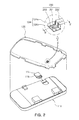
- FIG. 1 is a partially cut-away perspective view of a communications terminal according to an embodiment of the present invention
- FIG. 2 is a partially exploded perspective view of the communications terminal shown in FIG. 1 .
- a communications terminal 100 may include a terminal body 110, an antenna part 200, and a cover 120.
- the terminal body 110 may be formed by coupling main components of the communications terminal 100 to each other, and perform main functions of the communications terminal. To this end, the terminal body 110 may include a wireless module 115 therein.
- the wireless module 115 may transceive electrical signals and perform wireless communications with the outside.
- the wireless module 115 may be mounted on a circuit board, or the like, provided in the communications terminal and may be fixedly attached to the circuit board, and have memory card form to be insertedly fixed into a card insertion space formed in the terminal body 110 as shown in FIG. 2 .
- the wireless module 115 may include connection terminals 116 for electrically connecting the wireless module 115 and the antenna part 200 to be described below to each other.
- the cover 120 may form a portion of a case of the communications terminal 100 and may be coupled to the terminal body 110 to complete the communications terminal.
- the cover 120 may be a battery cover 120, provided in order to allow for the separation of a battery (not shown) from the terminal body 110 or to exchange the battery.
- the cover 120 according to the embodiment of the present invention is not limited thereto, but may be variously applied to any case forming the communications terminal 100.
- FIG. 3 is a cross-sectional view taken along line B-B' of FIG. 2 .
- the cover 120 may include an outer plate 123 and an inner plate 124.
- the outer plate 123 which forms an exterior of the cover may be formed to have a generally flat plate shape.
- a specific shape of the outer plate 123 may correspond to the exterior of the communications terminal 100.
- the inner plate 124 may be formed in an inner surface of the outer plate 123 to reinforce a thickness (that is, rigidity) of the cover 120. Further, the inner plate 124 may include a plate part 124a having an antenna pattern 220 disposed therein and a pin insertion part 124b having an exposure pad 201 formed therein.
- a thickness of the pin insertion part 124b may be greater than that of the plate part 124a. This configuration has been derived since an elastic pin 250 to be described below may be inserted into the pin insertion part 124b of the inner plate 124.
- the pin insertion part 124b of the inner plate 124 may have a size corresponding to that of the elastic pin 250. Therefore, in the case in which the elastic pin 250 is small, the thickness of the pin insertion part 124b may be identical to that of the plate part 124a. In the case in which the plate part 124a is thick, the pin insertion part 124b may have the same thickness as that of the plate part 124a.
- the pin insertion part 124b may have a pin insertion hole 125 formed therein.
- the pin insertion hole 125 may have an elastic pin 250 to be described below insertedly fixed therein. Therefore, the size and shape of the pin insertion hole 125 may correspond to an exterior of the elastic pin 250, and the pin insertion hole 125 may be formed at a position corresponding to that of a through-hole 202 of the exposure pad 201 to be described below.
- the pin insertion hole 125 may have an inner diameter equal to or slightly smaller than an outer diameter of the elastic pin 250 to be described below.
- the elastic pin 250 may be fitted into the pin insertion hole 125 and may be coupled to the pin insertion part 124b.
- the present invention is not limited thereto.
- the cover 120 may include the antenna part 200 interposed between the inner plate 124 and the outer plate 123.
- the antenna part 200 may include the antenna pattern 220 and the elastic pin 250.
- the antenna pattern 220 may only be formed of a metal radiator having a specific pattern or be formed to have an insulation layer on an outer portion of the metal radiator as needed.
- the antenna pattern may also be formed by using a metal pattern formed on a flexible film.
- the antenna pattern 220 may be formed by pressing a thin metal plate and be formed by using a metal pattern on a film (for example, a flexible substrate, or the like) by a sputtering method, a printing method, a plating method, a stamping method, a drawing method, a dispensing method, or the like.
- This antenna pattern 220 may be formed of copper, aluminum, or the like, and have a plating layer formed on an upper surface thereof.
- the plating layer is formed of nickel, gold, or the like.
- a plurality of exposure pads 201 may be formed at ends of the antenna pattern 220 to correspond to positions of the connection terminals 116 of the wireless module 115 described above.
- the exposure pad 201 according to the present embodiment may be formed at the ends of the antenna pattern 220 and include at least one through-hole 202 formed therein.
- This through-hole 202 may be disposed to correspond to the pin insertion hole 125 of the pin insertion part 124b as described above.
- the antenna pattern 220 may be interposed between the outer plate 123 and the inner plate 124. Therefore, the antenna pattern 220 is disposed in an inner portion of the cover 120, such that the antenna pattern 220 is not exposed to the outside.
- the elastic pin 250 may be inserted into the pin insertion hole 125 to electrically connect the connection terminals 116 of the wireless module 115 and the antenna pattern 220 to each other.
- FIG. 4 is a perspective view and a cross-sectional view schematically showing an elastic pin according to the present embodiment.
- the elastic pin 250 according to the present embodiment may include a contact part 252, an elastic supporting part 254, and a housing 256.
- the contact part 252 protruded outwardly to contact the outside, that is, the connection terminal 116, may have a tip shape.
- a lower surface of the contact part 252 may be formed as a smooth curved surface so that the contact part 252 may be easily inserted into the housing 256 when it contacts the wireless module 115 inserted from the side of the communications terminal, as shown in FIGS. 6A and 6B .
- the elastic supporting part 254 may be provided in order to provide elastic force to the contact part 252.
- the elastic supporting part 254 may be a coil spring having one end connected to the contact part 252 and the other end contacting an inner surface of the housing 256.
- the elastic supporting part 254 according to the embodiment of the present invention is not limited thereto. That is, various elastic providing devices such as a leaf spring, a torsion spring, and the like, may be used as long as they may provide elastic force to the contact part 252.
- the housing 256 may receive the contact part 252 and the elastic supporting part 254 therein and protect the contact part 252 and the elastic supporting part 254 form the outside. Therefore, the housing 256 may have various shapes according to a shape or a structure of the contact part 252 and the elastic supporting part 254.
- All of the contact part 252, the elastic supporting part 254, and the housing 256 of the elastic pin 250 may be formed of a metal material having high electric conductivity.
- the housing 256 of the elastic pin 250 may contact an inner surface of the exposure pad 201 to be electrically connected to the exposure pad 201.
- the elastic pin 250 may have a conductive line formed through the contact part 252, the elastic supporting part 254, and the housing 256 to electrically connect the connection terminal 116 (See FIG. 6B ) contacting the contact part 252 and the exposure pad 201 contacting the housing 256 to each other.
- the elastic pin 250 configured as described above may be maintained in a state in which the contact part 252 is basically protruded outwardly due to the elastic force provided by the elastic supporting part 254.
- the contact part 252 in this state may be protruded outwardly of the exposure pad 201 while penetrating through the through-hole 202 of the exposure pad 201.
- the contact part 252 may be inserted into the housing 256 (or into the exposure pad) while pressing the elastic supporting part 254.
- the elastic pin 250 according to the embodiment of the present invention is not limited to the above-mentioned configuration. That is, any device capable of being protruded outwardly of the exposure pad 201 and elastically moving by external force may be used.
- the antenna part 200 and the cover 120 are manufactured to be integrally formed. Therefore, a description of a general method of manufacturing a communications terminal will be omitted, and a method of integrally manufacturing a cover 120 and an antenna 200 will be mainly described.
- FIGS. 5A through 5D are views describing a method of manufacturing a communications terminal according to the embodiment of the present invention.
- the antenna pattern 220 may be coupled to the inner plate 124. This operation may be performed by disposing the antenna pattern 220 in a first mold (not shown) having the shape of the inner plate 124 formed therein and then injecting a resin thereinto.
- the first mold may have a similar structure to that of a second mold 300 (See FIG. 5C ) to be described below and is different from the second mold only in that an internal space thereof has a shape corresponding to that of the primary injection molding product.
- the elastic pin 250 may be coupled to the pin insertion hole 125 formed in the inner plate 124. As described above, the elastic pin 250 may be fitted into the pin insertion hole 125.
- the present invention is not limited thereto. That is, a method of fixing the elastic pin 250 by shielding an inlet of an upper end of the pin insertion hole 125, into which the elastic pin 250 is inserted, using a separate shielding member (not shown) may be also used.
- the shielding member may be connected to the antenna pattern 220 using a conductive member (for example, a solder paste, or the like).
- a conductive member for example, a solder paste, or the like.
- the elastic pin 250 may be fixedly inserted into the pin insertion hole 125 by various methods such as a method of fixing the elastic pin 250 by filling a filling material such as a resin in an inner wall of the pin insertion hole 125.
- an adhesive layer may be applied to the primary injection molding product.
- the adhesive layer may be formed by applying an adhesive such as a hot melt adhesive to an upper surface of the inner plate 124 or attaching an adhesive sheet thereto.
- This adhesive layer may be provided to firmly adhere the inner plate 124 and the outer plate 123 to each other. Meanwhile, in the case in which the inner plate 124 and the outer plate 123 are formed of the same material, the inner plate 124 and the outer plate 123 may be firmly adhered to each other even without a separate adhesive layer. Therefore, in this case, the adhesive layer may be omitted. That is, the adhesive layer may be selectively formed according to a material, or the like, of the inner plate 124 and the outer plate 123.
- the primary injection molding product may be disposed in the second mold 300.
- the second mold 300 may have the shape of the cover 120 formed therein.
- the second mold 300 may include an upper mold 300a and a lower mold 300b.
- An internal space 310 having the shape of the cover 120 may be formed in the second mold 300 by the upper and lower molds 300a and 300b.
- the primary injection molding product according to the present embodiment may be disposed in the internal space 310.
- the lower mold 300b on which the primary injection molding product is seated may have an inner surface formed such that the pin insertion part 124b of the primary injection molding product is inserted thereinto while being firmly closely adhered thereto. Therefore, during a resin injection process to be described below, a resin injected into the second mold 300 does not flow in a lower surface of the pin insertion part 124b, thereby preventing a problem in the driving of the elastic pin 250 in the case in which the resin flows in the pin insertion hole 125.
- the second mold 300 may include an introduction path 312 through which a molding material, that is, the resin, injected from the outside moves to the internal space of the second mold 300.
- a resin 128 may be injected into the second mold 300 through the introduction path 312 to complete the cover 120.
- the resin 128 injected into the mold 300 forms the outer plate 123 while covering the antenna pattern 220 on the primary injection molding product.
- the outer plate 123 may be formed on the upper portions of the inner plate 124 and the antenna pattern 220. Therefore, the cover 120, a final injection molding product, having the antenna pattern 220 interposed between the inner plate 124 and the outer plate 123, may be formed.
- the inner plate 124 and the outer plate 123 may be formed of the same material.
- the completed cover 120 may be integrally formed such that a boundary between the inner plate 124 and the outer plate 123 may not be readily distinguished.
- the present invention is not limited thereto, but may be variously applied as needed. That is, the inner plate 124 and the outer plate 123 may be formed of different materials.
- a contact structure between an antenna part and a wireless module according to the present embodiment is as follows.
- FIGS. 6A and 6B are views describing a contact structure between an antenna part and a wireless module according to the embodiment of the present invention.
- the wireless module 115 may have the form of the memory card to be insertedly fixed to the terminal body 110 in a sliding scheme.
- FIG. 6A shows a point in time at which the wireless module 115 enters the terminal body 110 while being slid.
- the elastic pin 250 may be maintained in a state in which the contact part 252 is protruded outwardly by as much as possible.
- the contact part 252 of the elastic pin 250 is pushed upwardly by the wireless module 115.
- the contact part 252 may firmly contact the connection terminal 116 of the wireless module 115 to be electrically connected thereto.
- the wireless module 115 is electrically connected to the antenna pattern 220, such that it may perform wireless transceiving through the antenna part 20 integrally 0 formed with the cover 120.
- the antenna pattern is embedded in the cover during a process of injecting the cover, a process of separately manufacturing an antenna pattern and then coupling the antenna pattern to a communications terminal as in the related art, or the like, may be omitted.
- the antenna pattern according to the embodiment of the present invention may be electrically connected to the wireless module using the elastic pin. Therefore, even in the case that a detachable wireless module is inserted into the terminal body in a sliding scheme, the wireless module and the antenna pattern may be easily electrically connected to each other.
- This configuration may be easily applied to a relatively large low frequency antenna. That is, a large low frequency antenna pattern may be embedded in the cover or the case of the communications terminal, and the wireless module may be inserted into the communications terminal to be used as necessary.
- the present invention may be usefully applied to a communications terminal, in which a wireless module is fixedly embedded and a cover coupled to an antenna part is opened and closed, as well as to a communications terminal including a detachable wireless module.
- the communications terminal and the method of manufacturing the same according to the embodiment of the present invention are not limited to the above-mentioned embodiments, but may be variously applied.
- the antenna pattern is embedded in the cover integrated with the cover by way of example in the foregoing embodiment, the present invention is not limited thereto. That is, the antenna pattern may be easily applied to any position of the case forming the terminal body, including the cover.
- the antenna pattern is embedded within the cover by way of example in the foregoing embodiment, the present invention is not limited thereto, but may be variously applied.
- the antenna pattern may be attached to one surface of the cover.
- the antenna is included in the communications terminal by way of example in the foregoing embodiment, the present invention is not limited thereto, but may be widely applied to all electronic devices including the antenna.
Landscapes
- Engineering & Computer Science (AREA)
- Manufacturing & Machinery (AREA)
- Mechanical Engineering (AREA)
- Signal Processing (AREA)
- Computer Networks & Wireless Communication (AREA)
- Telephone Set Structure (AREA)
- Details Of Aerials (AREA)
- Support Of Aerials (AREA)
Abstract
Description
- This application claims the priority of Korean Patent Application No.
10-2011-0041506 filed on May 2, 2011 - The present invention relates to a communications terminal in which an antenna and a case are integrally formed and a method of manufacturing the same.
- Recently, as communications terminals such as global positioning systems (GPSs), personal digital assistants (PDAs), cellular phones, wireless notebook computers, and the like, have been widely used and the portability thereof has been emphasized, slimness and lightness have been required therein. In addition, in order to satisfy these requirements, various technologies for reducing communications terminal volumes, while maintaining various functions thereof, have been developed.
- Accordingly, various attempts at reducing communications terminal volumes have been made with respect to antennas, essential components thereof.
- Generally, since an external antenna such as a rod antenna or a helical antenna, among communications terminal antennas, protrudes outwardly of the terminal by a predetermined length, miniaturization of a terminal may be difficult and portability thereof may be deteriorated. In addition, an external antenna may be damaged in the case that a communications terminal is dropped.
- Unlike the external antenna, in the case of an internal antenna mounted in the communications terminal, a risk of damage thereto may be reduced. However, it may be difficult to miniaturize the communications terminal due to a physical size of the internal antenna.
- Therefore, research into a technology of integrally forming an antenna radiator with a terminal case has been actively undertaken. For example, a method of attaching an antenna to a terminal case using an adhesive, a method of molding an antenna film in a case in a mold, and the like, have been suggested. In addition, various methods of electrically connecting an antenna attached to a case and a wireless module of a communications terminal to each other have been suggested.
- Particularly, in the case in which a wireless module is formed to have a form of a memory card, the wireless module is detachable from the communications terminal. Therefore, a method of easily electrically connecting a detachable wireless module having the form of a memory card, as described above, to an antenna attached to a case, has been demanded.
- An aspect of the present invention provides a communications terminal in which an antenna and a case are integrally formed, and a method of manufacturing the same.
- Another aspect of the present invention provides a communications terminal in which an antenna, formed integrally with a case, is easily electrically connected to a wireless module, and a method of manufacturing the same.
- Another aspect of the present invention provides a communications terminal in which a detachable wireless module, having a form of a memory card, may be electrically connected to an antenna formed integrally with a case, and a method of manufacturing the same.
- According to an aspect of the present invention, there is provided a communications terminal including: a terminal body; a case coupled to the terminal body to form an exterior of the terminal; and an antenna part including an antenna pattern integrally formed with the case and an elastic pin formed at one end of the antenna pattern to be electrically connected to a wireless module provided in the terminal body.
- The antenna part may include an exposure pad formed at a distal end of the antenna pattern, and the elastic pin may be partially protruded outwardly therefrom.
- The elastic pin may be inserted into a pin insertion hole formed in the case and electrically connected to the exposure pad.
- The antenna pattern may be embedded within the case, and the exposure pad may be exposed to an inner surface of the case.
- The elastic pin may include: a contact part protruded outwardly from the exposure pad; an elastic supporting part connected to the contact part to thereby provide elastic force to the contact part; and a housing receiving the contact part and the elastic supporting part therein.
- The elastic supporting part may be formed of a coil spring.
- The case may include an outer plate forming an exterior of the terminal, and an inner plate coupled to an inner surface of the outer plate, and the antenna pattern may be interposed between the inner plate and the outer plate.
- The exposure pad may be exposed to an inner surface of the inner plate.
- The wireless module may be detachable from the terminal body.
- The wireless module may be detached from the terminal body in a sliding scheme.
- The inner plate and the outer plate may be formed of the same material.
- According to another aspect of the present invention, there is provided a method of manufacturing a communications terminal, the method including: preparing a primary injection molding product in which an antenna pattern is coupled to an inner plate; coupling an elastic pin to the inner plate to be electrically connected to the antenna pattern of the primary injection molding product; and forming an outer plate on one surface of the primary injection molding product.
- The preparing of the primary injection molding product may include: disposing the antenna pattern in a first mold; and forming the inner plate by injecting a resin into the first mold.
- The elastic pin may include a contact part elastically contacting the outside, and the coupling of the elastic pin to the inner plate may include allowing the contact part to be protruded outwardly while penetrating through the antenna pattern.
- The forming of the outer plate on one surface of the primary injection molding product may include: disposing the primary injection molding product in a second mold; and forming the outer plate while covering the antenna pattern by injecting a resin into the second mold.
- The above and other aspects, features and other advantages of the present invention will be more clearly understood from the following detailed description taken in conjunction with the accompanying drawings, in which:
-
FIG. 1 is a partially cut-away perspective view of a communications terminal according to an embodiment of the present invention; -
FIG. 2 is a partially exploded perspective view of the communications terminal shown inFIG. 1 ; -
FIG. 3 is a cross-sectional view taken along line B-B' ofFIG. 2 ; -
FIG. 4 is a perspective view and a cross-sectional view schematically showing an elastic pin according to an embodiment of the present invention; -
FIGS. 5A through 5D are views describing a method of manufacturing a communications terminal according to an embodiment of the present invention; and -
FIGS. 6A and 6B are views describing a contact structure between an antenna part and a wireless module according to an embodiment of the present invention. - Prior to a detailed description of the present invention, the terms or words, which are used in the specification and claims to be described below, should not be construed as having typical or dictionary meanings. The terms or words should be construed in conformity with the technical idea of the present invention on the basis of the principle that the inventor(s) can appropriately define terms in order to describe his or her invention in the best way. Embodiments described in the specification and structures illustrated in drawings are merely exemplary embodiments of the present invention. Thus, it is intended that the present invention covers the modifications and variations of this invention, provided they fall within the scope of their equivalents at the time of filing this application.
- Exemplary embodiments of the present invention will be described in detail with reference to the accompanying drawings. The same reference numerals will be used throughout to designate the same or like elements in the accompanying drawings. Moreover, detailed descriptions related to well-known functions or configurations will be ruled out in order not to unnecessarily obscure subject matters of the present invention. In the drawings, the shapes and dimensions of some elements may be exaggerated, omitted or schematically illustrated. Also, the size of each element does not entirely reflect an actual size.
- Hereinafter, embodiments of the present invention will be described in detail with reference to the accompanying drawings.
-
FIG. 1 is a partially cut-away perspective view of a communications terminal according to an embodiment of the present invention; andFIG. 2 is a partially exploded perspective view of the communications terminal shown inFIG. 1 . - Referring to
FIGS. 1 and2 , acommunications terminal 100 according to an embodiment of the present invention may include aterminal body 110, anantenna part 200, and acover 120. - The
terminal body 110 may be formed by coupling main components of thecommunications terminal 100 to each other, and perform main functions of the communications terminal. To this end, theterminal body 110 may include awireless module 115 therein. - The
wireless module 115 may transceive electrical signals and perform wireless communications with the outside. Thewireless module 115 may be mounted on a circuit board, or the like, provided in the communications terminal and may be fixedly attached to the circuit board, and have memory card form to be insertedly fixed into a card insertion space formed in theterminal body 110 as shown inFIG. 2 . - In addition, the
wireless module 115 may includeconnection terminals 116 for electrically connecting thewireless module 115 and theantenna part 200 to be described below to each other. - The
cover 120 may form a portion of a case of thecommunications terminal 100 and may be coupled to theterminal body 110 to complete the communications terminal. Thecover 120 may be abattery cover 120, provided in order to allow for the separation of a battery (not shown) from theterminal body 110 or to exchange the battery. However, thecover 120 according to the embodiment of the present invention is not limited thereto, but may be variously applied to any case forming thecommunications terminal 100. -
FIG. 3 is a cross-sectional view taken along line B-B' ofFIG. 2 . - Referring to
FIG.3 , thecover 120 according to the embodiment of the present invention may include anouter plate 123 and aninner plate 124. - The
outer plate 123 which forms an exterior of the cover may be formed to have a generally flat plate shape. A specific shape of theouter plate 123 may correspond to the exterior of thecommunications terminal 100. - The
inner plate 124 may be formed in an inner surface of theouter plate 123 to reinforce a thickness (that is, rigidity) of thecover 120. Further, theinner plate 124 may include aplate part 124a having anantenna pattern 220 disposed therein and apin insertion part 124b having anexposure pad 201 formed therein. - Here, a thickness of the
pin insertion part 124b may be greater than that of theplate part 124a. This configuration has been derived since anelastic pin 250 to be described below may be inserted into thepin insertion part 124b of theinner plate 124. - That is, the
pin insertion part 124b of theinner plate 124 may have a size corresponding to that of theelastic pin 250. Therefore, in the case in which theelastic pin 250 is small, the thickness of thepin insertion part 124b may be identical to that of theplate part 124a. In the case in which theplate part 124a is thick, thepin insertion part 124b may have the same thickness as that of theplate part 124a. - The
pin insertion part 124b may have apin insertion hole 125 formed therein. Thepin insertion hole 125 may have anelastic pin 250 to be described below insertedly fixed therein. Therefore, the size and shape of thepin insertion hole 125 may correspond to an exterior of theelastic pin 250, and thepin insertion hole 125 may be formed at a position corresponding to that of a through-hole 202 of theexposure pad 201 to be described below. - Meanwhile, the
pin insertion hole 125 may have an inner diameter equal to or slightly smaller than an outer diameter of theelastic pin 250 to be described below. In this case, theelastic pin 250 may be fitted into thepin insertion hole 125 and may be coupled to thepin insertion part 124b. However, the present invention is not limited thereto. - In addition, the
cover 120 according to the present embodiment may include theantenna part 200 interposed between theinner plate 124 and theouter plate 123. - The
antenna part 200 may include theantenna pattern 220 and theelastic pin 250. - The
antenna pattern 220 may only be formed of a metal radiator having a specific pattern or be formed to have an insulation layer on an outer portion of the metal radiator as needed. In addition, the antenna pattern may also be formed by using a metal pattern formed on a flexible film. - Therefore, the
antenna pattern 220 according to the present embodiment may be formed by pressing a thin metal plate and be formed by using a metal pattern on a film (for example, a flexible substrate, or the like) by a sputtering method, a printing method, a plating method, a stamping method, a drawing method, a dispensing method, or the like. - This
antenna pattern 220 may be formed of copper, aluminum, or the like, and have a plating layer formed on an upper surface thereof. Here, the plating layer is formed of nickel, gold, or the like. - In addition, a plurality of
exposure pads 201 may be formed at ends of theantenna pattern 220 to correspond to positions of theconnection terminals 116 of thewireless module 115 described above. Theexposure pad 201 according to the present embodiment may be formed at the ends of theantenna pattern 220 and include at least one through-hole 202 formed therein. - This through-
hole 202 may be disposed to correspond to thepin insertion hole 125 of thepin insertion part 124b as described above. - The
antenna pattern 220, with the exception of theexposure pad 201, may be interposed between theouter plate 123 and theinner plate 124. Therefore, theantenna pattern 220 is disposed in an inner portion of thecover 120, such that theantenna pattern 220 is not exposed to the outside. - The
elastic pin 250 may be inserted into thepin insertion hole 125 to electrically connect theconnection terminals 116 of thewireless module 115 and theantenna pattern 220 to each other. -
FIG. 4 is a perspective view and a cross-sectional view schematically showing an elastic pin according to the present embodiment. Referring toFIG. 4 , theelastic pin 250 according to the present embodiment may include acontact part 252, an elastic supportingpart 254, and ahousing 256. - The
contact part 252, protruded outwardly to contact the outside, that is, theconnection terminal 116, may have a tip shape. According to the present embodiment, a lower surface of thecontact part 252 may be formed as a smooth curved surface so that thecontact part 252 may be easily inserted into thehousing 256 when it contacts thewireless module 115 inserted from the side of the communications terminal, as shown inFIGS. 6A and 6B . - The elastic supporting
part 254 may be provided in order to provide elastic force to thecontact part 252. To this end, the elastic supportingpart 254 may be a coil spring having one end connected to thecontact part 252 and the other end contacting an inner surface of thehousing 256. However, the elastic supportingpart 254 according to the embodiment of the present invention is not limited thereto. That is, various elastic providing devices such as a leaf spring, a torsion spring, and the like, may be used as long as they may provide elastic force to thecontact part 252. - The
housing 256 may receive thecontact part 252 and the elastic supportingpart 254 therein and protect thecontact part 252 and the elastic supportingpart 254 form the outside. Therefore, thehousing 256 may have various shapes according to a shape or a structure of thecontact part 252 and the elastic supportingpart 254. - All of the
contact part 252, the elastic supportingpart 254, and thehousing 256 of theelastic pin 250 may be formed of a metal material having high electric conductivity. In addition, when theelastic pin 250 is inserted into thepin insertion hole 125, thehousing 256 of theelastic pin 250 may contact an inner surface of theexposure pad 201 to be electrically connected to theexposure pad 201. - Therefore, the
elastic pin 250 may have a conductive line formed through thecontact part 252, the elastic supportingpart 254, and thehousing 256 to electrically connect the connection terminal 116 (SeeFIG. 6B ) contacting thecontact part 252 and theexposure pad 201 contacting thehousing 256 to each other. - The
elastic pin 250 configured as described above may be maintained in a state in which thecontact part 252 is basically protruded outwardly due to the elastic force provided by the elastic supportingpart 254. Thecontact part 252 in this state may be protruded outwardly of theexposure pad 201 while penetrating through the through-hole 202 of theexposure pad 201. - In addition, in the case in which external force stronger than the elastic force is applied to the
contact part 252, thecontact part 252 may be inserted into the housing 256 (or into the exposure pad) while pressing the elastic supportingpart 254. - Meanwhile, the
elastic pin 250 according to the embodiment of the present invention is not limited to the above-mentioned configuration. That is, any device capable of being protruded outwardly of theexposure pad 201 and elastically moving by external force may be used. - Next, a method of manufacturing a communications terminal according to an embodiment of the present invention will be described in detail. The configuration of the
communications terminal 100 described above will be further clear from the following description of a method of manufacturing a communications terminal. - In the
communications terminal 100 according to the present embodiment, theantenna part 200 and thecover 120 are manufactured to be integrally formed. Therefore, a description of a general method of manufacturing a communications terminal will be omitted, and a method of integrally manufacturing acover 120 and anantenna 200 will be mainly described. -
FIGS. 5A through 5D are views describing a method of manufacturing a communications terminal according to the embodiment of the present invention. - Referring to
FIG. 5A through 5D , in the method of manufacturing thecommunications terminal 100 according to the present embodiment, as shown inFIG. 5A , theantenna pattern 220 may be coupled to theinner plate 124. This operation may be performed by disposing theantenna pattern 220 in a first mold (not shown) having the shape of theinner plate 124 formed therein and then injecting a resin thereinto. - Therefore, a primary injection molding product in which the
antenna pattern 220 is coupled to theinner plate 124 is formed. Meanwhile, the first mold may have a similar structure to that of a second mold 300 (SeeFIG. 5C ) to be described below and is different from the second mold only in that an internal space thereof has a shape corresponding to that of the primary injection molding product. - Next, as shown in
FIG. 5B , theelastic pin 250 may be coupled to thepin insertion hole 125 formed in theinner plate 124. As described above, theelastic pin 250 may be fitted into thepin insertion hole 125. - However, the present invention is not limited thereto. That is, a method of fixing the
elastic pin 250 by shielding an inlet of an upper end of thepin insertion hole 125, into which theelastic pin 250 is inserted, using a separate shielding member (not shown) may be also used. Here, the shielding member may be connected to theantenna pattern 220 using a conductive member (for example, a solder paste, or the like). In this case, since theelastic pin 250 may be electrically connected to theantenna pattern 220 by the shielding member as well as anexposure pad 201, the reliability of connection may be secured. - In addition, according to the embodiment of the present invention, the
elastic pin 250 may be fixedly inserted into thepin insertion hole 125 by various methods such as a method of fixing theelastic pin 250 by filling a filling material such as a resin in an inner wall of thepin insertion hole 125. - After the primary injection molding product is completed, an adhesive layer may be applied to the primary injection molding product. The adhesive layer may be formed by applying an adhesive such as a hot melt adhesive to an upper surface of the
inner plate 124 or attaching an adhesive sheet thereto. - This adhesive layer may be provided to firmly adhere the
inner plate 124 and theouter plate 123 to each other. Meanwhile, in the case in which theinner plate 124 and theouter plate 123 are formed of the same material, theinner plate 124 and theouter plate 123 may be firmly adhered to each other even without a separate adhesive layer. Therefore, in this case, the adhesive layer may be omitted. That is, the adhesive layer may be selectively formed according to a material, or the like, of theinner plate 124 and theouter plate 123. - Then, as shown in
FIG. 5C , the primary injection molding product may be disposed in thesecond mold 300. Thesecond mold 300 may have the shape of thecover 120 formed therein. - The
second mold 300 may include anupper mold 300a and alower mold 300b. Aninternal space 310 having the shape of thecover 120 may be formed in thesecond mold 300 by the upper andlower molds internal space 310. - Meanwhile, the
lower mold 300b on which the primary injection molding product is seated may have an inner surface formed such that thepin insertion part 124b of the primary injection molding product is inserted thereinto while being firmly closely adhered thereto. Therefore, during a resin injection process to be described below, a resin injected into thesecond mold 300 does not flow in a lower surface of thepin insertion part 124b, thereby preventing a problem in the driving of theelastic pin 250 in the case in which the resin flows in thepin insertion hole 125. - In addition, the
second mold 300 may include anintroduction path 312 through which a molding material, that is, the resin, injected from the outside moves to the internal space of thesecond mold 300. - After the primary injection molding product is seated in the
internal space 310 of thesecond mold 300, as shown inFIG. 5D , a resin 128 may be injected into thesecond mold 300 through theintroduction path 312 to complete thecover 120. Here, the resin 128 injected into themold 300 forms theouter plate 123 while covering theantenna pattern 220 on the primary injection molding product. - Therefore, as shown in
FIG. 3 , theouter plate 123 may be formed on the upper portions of theinner plate 124 and theantenna pattern 220. Therefore, thecover 120, a final injection molding product, having theantenna pattern 220 interposed between theinner plate 124 and theouter plate 123, may be formed. - Meanwhile, the
inner plate 124 and theouter plate 123 may be formed of the same material. In this case, the completedcover 120 may be integrally formed such that a boundary between theinner plate 124 and theouter plate 123 may not be readily distinguished. - However, the present invention is not limited thereto, but may be variously applied as needed. That is, the
inner plate 124 and theouter plate 123 may be formed of different materials. - Next, a contact structure between an antenna part and a wireless module according to the present embodiment is as follows.
-
FIGS. 6A and 6B are views describing a contact structure between an antenna part and a wireless module according to the embodiment of the present invention. - As described above, the
wireless module 115 according to the present embodiment may have the form of the memory card to be insertedly fixed to theterminal body 110 in a sliding scheme. -
FIG. 6A shows a point in time at which thewireless module 115 enters theterminal body 110 while being slid. During this operation, theelastic pin 250 may be maintained in a state in which thecontact part 252 is protruded outwardly by as much as possible. - Then, as shown in
FIG. 6B , when thewireless module 115 is completely inserted into the circuit board, thecontact part 252 of theelastic pin 250 is pushed upwardly by thewireless module 115. In this case, since thecontact part 252 is continuously applied with downward force by the elastic supportingpart 254, thecontact part 252 may firmly contact theconnection terminal 116 of thewireless module 115 to be electrically connected thereto. - Therefore, the
wireless module 115 is electrically connected to theantenna pattern 220, such that it may perform wireless transceiving through the antenna part 20 integrally 0 formed with thecover 120. - As set forth above, in the case of the communications terminal according to the embodiment of the present invention, since the antenna pattern is embedded in the cover during a process of injecting the cover, a process of separately manufacturing an antenna pattern and then coupling the antenna pattern to a communications terminal as in the related art, or the like, may be omitted.
- In addition, the antenna pattern according to the embodiment of the present invention may be electrically connected to the wireless module using the elastic pin. Therefore, even in the case that a detachable wireless module is inserted into the terminal body in a sliding scheme, the wireless module and the antenna pattern may be easily electrically connected to each other.
- This configuration may be easily applied to a relatively large low frequency antenna. That is, a large low frequency antenna pattern may be embedded in the cover or the case of the communications terminal, and the wireless module may be inserted into the communications terminal to be used as necessary.
- In addition, the present invention may be usefully applied to a communications terminal, in which a wireless module is fixedly embedded and a cover coupled to an antenna part is opened and closed, as well as to a communications terminal including a detachable wireless module.
- Meanwhile, the communications terminal and the method of manufacturing the same according to the embodiment of the present invention are not limited to the above-mentioned embodiments, but may be variously applied. Although the antenna pattern is embedded in the cover integrated with the cover by way of example in the foregoing embodiment, the present invention is not limited thereto. That is, the antenna pattern may be easily applied to any position of the case forming the terminal body, including the cover.
- In addition, although the antenna pattern is embedded within the cover by way of example in the foregoing embodiment, the present invention is not limited thereto, but may be variously applied. For example, the antenna pattern may be attached to one surface of the cover.
- Further, although the antenna is included in the communications terminal by way of example in the foregoing embodiment, the present invention is not limited thereto, but may be widely applied to all electronic devices including the antenna.
- While the present invention has been shown and described in connection with the embodiments, it will be apparent to those skilled in the art that modifications and variations can be made without departing from the spirit and scope of the invention as defined by the appended claims.
Claims (15)
- A communications terminal comprising:a terminal body;a case coupled to the terminal body to form an exterior of the terminal; andan antenna part including an antenna pattern integrally formed with the case and an elastic pin formed at one end of the antenna pattern to be electrically connected to a wireless module provided in the terminal body.
- The communications terminal of claim 1, wherein the antenna part includes an exposure pad formed at a distal end of the antenna pattern, and
the elastic pin is partially protruded outwardly therefrom. - The communications terminal of claim 2, wherein the elastic pin is inserted into a pin insertion hole formed in the case and is electrically connected to the exposure pad.
- The communications terminal of claim 2, wherein the antenna pattern is embedded within the case, and
the exposure pad is exposed to an inner surface of the case. - The communications terminal of claim 2, wherein the elastic pin includes:a contact part protruded outwardly from the exposure pad;an elastic supporting part connected to the contact part to thereby provide elastic force to the contact part; anda housing receiving the contact part and the elastic supporting part therein.
- The communications terminal of claim 5, wherein the elastic supporting part is formed of a coil spring.
- The communications terminal of claim 2, wherein the case includes:an outer plate forming an exterior of the terminal; andan inner plate coupled to an inner surface of the outer plate,wherein the antenna pattern is interposed between the inner plate and the outer plate.
- The communications terminal of claim 7, wherein the exposure pad is exposed to an inner surface of the inner plate.
- The communications terminal of claim 1, wherein the wireless module is detachable from the terminal body.
- The communications terminal of claim 9, wherein the wireless module is detached from the terminal body in a sliding scheme.
- The communications terminal of claim 7, wherein the inner plate and the outer plate are formed of the same material.
- A method of manufacturing a communications terminal, the method comprising:preparing a primary injection molding product in which an antenna pattern is coupled to an inner plate;coupling an elastic pin to the inner plate to be electrically connected to the antenna pattern of the primary injection molding product; andforming an outer plate on one surface of the primary injection molding product.
- The method of claim 12, wherein the preparing of the primary injection molding product includes:disposing the antenna pattern in a first mold; andforming the inner plate by injecting a resin into the first mold.
- The method of claim 12, wherein the elastic pin includes a contact part elastically contacting the outside, and
the coupling of the elastic pin to the inner plate includes allowing the contact part to be protruded outwardly while penetrating through the antenna pattern. - The method of claim 12, wherein the forming of the outer plate on one surface of the primary injection molding product includes:disposing the primary injection molding product in a second mold; andforming the outer plate while covering the antenna pattern by injecting a resin into the second mold.
Applications Claiming Priority (1)
| Application Number | Priority Date | Filing Date | Title |
|---|---|---|---|
| KR1020110041506A KR20120123895A (en) | 2011-05-02 | 2011-05-02 | Terminal for communication and method of manufacturing the same |
Publications (2)
| Publication Number | Publication Date |
|---|---|
| EP2520406A2 true EP2520406A2 (en) | 2012-11-07 |
| EP2520406A3 EP2520406A3 (en) | 2013-06-05 |
Family
ID=46046050
Family Applications (1)
| Application Number | Title | Priority Date | Filing Date |
|---|---|---|---|
| EP12275041.7A Withdrawn EP2520406A3 (en) | 2011-05-02 | 2012-04-10 | Communications terminal and method of manufacturing the same |
Country Status (4)
| Country | Link |
|---|---|
| US (1) | US20120281384A1 (en) |
| EP (1) | EP2520406A3 (en) |
| JP (1) | JP2012235451A (en) |
| KR (1) | KR20120123895A (en) |
Families Citing this family (4)
| Publication number | Priority date | Publication date | Assignee | Title |
|---|---|---|---|---|
| JP5700055B2 (en) | 2013-01-17 | 2015-04-15 | 株式会社村田製作所 | Antenna device |
| KR101547131B1 (en) * | 2014-03-20 | 2015-08-25 | 스카이크로스 인코포레이티드 | Antenna with radiator fixed by fusion, and manufacturing method thereof |
| US9596331B2 (en) * | 2015-01-10 | 2017-03-14 | Seungman Kim | Electronic apparatus having interface to wirelessly communicate with internal wireless device disposed in a housing of the electronic apparatus and a method thereof |
| DE102018124028A1 (en) * | 2018-09-28 | 2020-04-02 | Lisa Dräxlmaier GmbH | SENSOR DEVICE, POWER SUPPLY SYSTEM AND METHOD |
Family Cites Families (11)
| Publication number | Priority date | Publication date | Assignee | Title |
|---|---|---|---|---|
| FR2775373A1 (en) * | 1998-02-24 | 1999-08-27 | Jean Pierre Gerbaulet | CONNECTOR AND CHIP CARD READER COMPRISING SUCH A CONNECTOR |
| JP2002064316A (en) * | 2000-08-17 | 2002-02-28 | Sony Corp | Antenna device and portable wireless device |
| JP4734808B2 (en) * | 2001-09-13 | 2011-07-27 | 株式会社村田製作所 | Card type wireless communication terminal device |
| JP2003234668A (en) * | 2002-02-12 | 2003-08-22 | Matsushita Electric Ind Co Ltd | Communication equipment |
| KR100905858B1 (en) * | 2007-08-21 | 2009-07-02 | 삼성전기주식회사 | Case integrated antenna and manufacturing method |
| TWM354252U (en) * | 2008-11-21 | 2009-04-01 | Cheng Uei Prec Ind Co Ltd | Pogo pin connector |
| KR100955510B1 (en) * | 2009-04-23 | 2010-04-30 | 삼성전기주식회사 | Antenna pattern frame, method and mould for manufacturing the same |
| KR100945123B1 (en) * | 2009-04-23 | 2010-03-02 | 삼성전기주식회사 | Antenna pattern frame, method and mould for manufacturing the same,and electronic device |
| JP5442376B2 (en) * | 2009-09-28 | 2014-03-12 | 京セラ株式会社 | Portable electronic devices |
| KR20120013838A (en) * | 2010-08-06 | 2012-02-15 | 삼성전기주식회사 | Electronic device with antenna pattern embedded in case and manufacturing method |
| KR101153673B1 (en) * | 2010-12-29 | 2012-06-18 | 삼성전기주식회사 | Sim card assembly, method for manufacturing the same, and electronic device including the same |
-
2011
- 2011-05-02 KR KR1020110041506A patent/KR20120123895A/en not_active Withdrawn
-
2012
- 2012-03-28 JP JP2012073415A patent/JP2012235451A/en active Pending
- 2012-04-10 EP EP12275041.7A patent/EP2520406A3/en not_active Withdrawn
- 2012-05-01 US US13/461,321 patent/US20120281384A1/en not_active Abandoned
Non-Patent Citations (1)
| Title |
|---|
| None |
Also Published As
| Publication number | Publication date |
|---|---|
| EP2520406A3 (en) | 2013-06-05 |
| US20120281384A1 (en) | 2012-11-08 |
| JP2012235451A (en) | 2012-11-29 |
| KR20120123895A (en) | 2012-11-12 |
Similar Documents
| Publication | Publication Date | Title |
|---|---|---|
| EP2421089A2 (en) | Electronic device having antenna pattern embedded in case and method for manufacturing the same | |
| EP2418731A2 (en) | Electronic device having transmission line pattern embedded in case and method for manufacturing the same | |
| US8982009B2 (en) | Antenna pattern frame, method and mold for manufacturing the same, and electronic device | |
| US8618989B2 (en) | Electronic device case, method and mold for manufacturing the same, and mobile communications terminal | |
| EP2403065A2 (en) | Electronic device case having antenna pattern embedded therein, method for manufacturing the same, mold for manufacturing antenna pattern frame, and electronic device | |
| KR101153673B1 (en) | Sim card assembly, method for manufacturing the same, and electronic device including the same | |
| EP2386401A1 (en) | Case of electronic device having antenna pattern embedde therein, and mold therefor and mthod of manufacturing thereof | |
| EP2367231A1 (en) | Electronic device case, mold for manufacturing the same, and mobile communications terminal | |
| EP2361744A1 (en) | Antenna pattern frame and mold for manufacturing electronic device case including the same | |
| CN105048083A (en) | Antenna pattern frame and method of manufacturing the same | |
| EP2284947A1 (en) | Antenna pattern frame, method and mold for manufacturing the same, electronic device case having antenna pattern frame embedded therein, and method for manufacturing the same | |
| US20100271265A1 (en) | Antenna pattern frame and method and mold for manufacturing the same | |
| EP2386400A1 (en) | Case of electronic device having antenna pattern frame embedded therein, mold therefor and method of manufacturing thereof | |
| JP5951540B2 (en) | Method for manufacturing electronic device case including antenna pattern frame, and method for manufacturing electronic device including electronic device case | |
| EP2387106A1 (en) | Case of electronic device having low frequency antenna pattern embedded therein, mold therefor and method of manufacturing thereof | |
| US20120281384A1 (en) | Communications terminal and method of manufacturing the same | |
| KR20160055573A (en) | Antenna module and electronic device including the same | |
| KR20110092975A (en) | Portable terminal with stabilized contact structure using permanent magnet | |
| WO2012168536A1 (en) | Two shot molding antenna with conductive plastic | |
| KR20110034320A (en) | Contact structure of built-in antenna and mobile communication terminal including same | |
| KR20110124670A (en) | Case of electronic device with antenna pattern embedded, manufacturing mold and manufacturing method thereof |
Legal Events
| Date | Code | Title | Description |
|---|---|---|---|
| PUAI | Public reference made under article 153(3) epc to a published international application that has entered the european phase |
Free format text: ORIGINAL CODE: 0009012 |
|
| AK | Designated contracting states |
Kind code of ref document: A2 Designated state(s): AL AT BE BG CH CY CZ DE DK EE ES FI FR GB GR HR HU IE IS IT LI LT LU LV MC MK MT NL NO PL PT RO RS SE SI SK SM TR |
|
| AX | Request for extension of the european patent |
Extension state: BA ME |
|
| PUAL | Search report despatched |
Free format text: ORIGINAL CODE: 0009013 |
|
| AK | Designated contracting states |
Kind code of ref document: A3 Designated state(s): AL AT BE BG CH CY CZ DE DK EE ES FI FR GB GR HR HU IE IS IT LI LT LU LV MC MK MT NL NO PL PT RO RS SE SI SK SM TR |
|
| AX | Request for extension of the european patent |
Extension state: BA ME |
|
| RIC1 | Information provided on ipc code assigned before grant |
Ipc: H01Q 1/24 20060101ALI20130426BHEP Ipc: B29L 31/34 20060101ALN20130426BHEP Ipc: H01Q 7/00 20060101ALI20130426BHEP Ipc: H04M 1/02 20060101ALI20130426BHEP Ipc: B29C 45/14 20060101AFI20130426BHEP Ipc: B29C 45/16 20060101ALI20130426BHEP |
|
| STAA | Information on the status of an ep patent application or granted ep patent |
Free format text: STATUS: THE APPLICATION IS DEEMED TO BE WITHDRAWN |
|
| 18D | Application deemed to be withdrawn |
Effective date: 20131206 |