EP2519079B1 - Solid light-emitting element lighting device and illumination fixture using the same - Google Patents
Solid light-emitting element lighting device and illumination fixture using the same Download PDFInfo
- Publication number
- EP2519079B1 EP2519079B1 EP12159970.8A EP12159970A EP2519079B1 EP 2519079 B1 EP2519079 B1 EP 2519079B1 EP 12159970 A EP12159970 A EP 12159970A EP 2519079 B1 EP2519079 B1 EP 2519079B1
- Authority
- EP
- European Patent Office
- Prior art keywords
- switching element
- lighting device
- current
- solid light
- emitting element
- Prior art date
- Legal status (The legal status is an assumption and is not a legal conclusion. Google has not performed a legal analysis and makes no representation as to the accuracy of the status listed.)
- Not-in-force
Links
Images


Classifications
-
- H—ELECTRICITY
- H05—ELECTRIC TECHNIQUES NOT OTHERWISE PROVIDED FOR
- H05B—ELECTRIC HEATING; ELECTRIC LIGHT SOURCES NOT OTHERWISE PROVIDED FOR; CIRCUIT ARRANGEMENTS FOR ELECTRIC LIGHT SOURCES, IN GENERAL
- H05B45/00—Circuit arrangements for operating light-emitting diodes [LED]
- H05B45/30—Driver circuits
- H05B45/37—Converter circuits
Definitions
- the present invention relates to a solid light-emitting element lighting device and to an illumination fixture using the same.
- the LED lighting device for supplying lighting power to an LED illumination module (for example, refer to JPT 2006-511078 and paragraphs [0015] to [0017] and Fig. 7 to Fig. 9 ).
- the LED lighting device includes: a control switch Q3 for being turned on and off in accordance with a dual signal including a low-frequency burst of high-frequency pulse, the control switch Q3 being connected to an LED illumination module 104 in series; an inductor L2 for accumulating energy when the control switch Q3 is turned on, the inductor similarly being connected to the LED illumination module 104 in series; and a diode D2 for regenerating the energy accumulated in the inductor L2 to the LED illumination module 104 at the turning-off of the control switch Q3.
- the above-mentioned dual signal is an AND output of a high-frequency drive pulse and a low-frequency PWM signal to the control switch Q3, an average current flowing to the LED illumination module 104 is varied by changing a duty ratio of the PWM signal, and thus a light intensity outputted from the LED illumination module 104 is changed (so-called burst dimming).
- US 2007/0188112 A1 shows a solid light-emitting element lighting device comprising: a series circuit of an inductor and a switching element that are connected between output terminals of a direct-current power source via a load; a diode for regenerating, during turning-off of the switching element, energy accumulated during turning-on of the switching element in the inductor to the load; and a control circuit part for controlling on and off of the switching element.
- the control circuit part includes a drive signal generation part for generating the drive signal whose pulse width varies in accordance with an amplitude of a load current.
- the device in order to prevent an excessive current flowing through the load, the device according to US 2007/0188112 A1 further contains a blocking means that blocks a PWM signal so that the drive signal is low if the current flowing through the load exceeds a preset value when the PWM signal is high.
- the current through the load is determined by measuring a shunt voltage that is subtracted from the high level voltage of the PWM signal and the difference is compared with a preset voltage value.
- WO 2010/046065 A1 proposes a lighting device for an LED module.
- a diode for regenerating, during turning-off of the switching element, energy accumulated during turning-on of the switching element in the inductor to the LED module is provided.
- a capacitor is connected parallel with the LED module to minimize ripples of the current flowing through the LED module.
- the switching element ist preferably switched when the current through the switching element is zero to avoid losses.
- the high-frequency drive pulse to the control switch Q3 is the AND output including the low-frequency PWM signal, and when an edge of the above-mentioned PWM signal is inputted during the turning-on of the control switch Q3, the drive pulse to the control switch Q3 becomes Low.
- the on-period of the control switch Q3 is changed due to the variation of the low-frequency PWM signal, and accordingly an LED current, that is, an optical output of the LED illumination module 104 varies.
- the regeneration current of the inductor L2 flows to the LED illumination module 104 via the diode D2; however, even when the above-mentioned PWM signal varies, the LED current does not change during the period. That is, despite the variation of the PWM signal, the optical output of the LED module 104 does not change.
- Fig. 8 is a time chart of the case where the control switch Q3 is operated in a critical mode (a mode in which the control switch Q3 is switched from being turned off to being turned on at timing when the current flowing to the inductor L2 becomes zero).
- a critical mode a mode in which the control switch Q3 is switched from being turned off to being turned on at timing when the current flowing to the inductor L2 becomes zero.
- a load current I1 of the LED illumination module 104 will increase by one cycle of the drive signal (the broken line in Fig. 8 ).
- the optical output to the duty variation will be stepwise as shown in Fig. 9 .
- the optical output difference of the one step is equivalent to the optical output of the one cycle of the high-frequency drive pulse for the control switch Q3, and accordingly the stepwise variation of the optical output can be watched.
- the stepwise variation will be more apparent.
- the ratio of the period where the optical output does not vary in the sweeping of the PWM signal is large, and consequently there causes a problem that the optical output appears to vary in a stepwise fashion.
- the present invention is achieved in consideration of the above-mentioned problems, and a purpose of the present invention is to provide a solid light-emitting element lighting device and an illumination fixture using the same that are able to smoothly change the optical output in the sweeping of the PWM signal for dimming.
- a solid light-emitting element lighting device of the present invention includes the features of claim 1.
- control circuit part includes a zero current detection circuit for detection that a current flowing to the inductor becomes zero, and switches the switching element from being turned off to being turned on in synchronization with detection timing of the zero current detection circuit.
- control circuit part switches the switching element to be turned on before the current flowing to the inductor during the turning-off of the switching element becomes zero.
- the direct-current power source includes an AC-DC converter or a DC-DC converter to which a detection result of the load voltage is feed backed and that controls an output voltage to be a voltage proportional to the detection result, and includes a voltage detection part for detecting the load voltage and feed backing the load voltage to the direct-current power source.
- the direct-current power source includes the AC-DC converter, and a frequency of the PWM signal is set to 600Hz or multiples of 600Hz.
- An illumination fixture of the present invention includes: the solid light-emitting element lighting device according to any one of claims 1 to 5; and a solid light-emitting element to which lighting power is supplied from the solid light-emitting element lighting device.
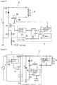
- Fig. 1 is a schematic circuit view showing an LED lighting device (a solid light-light emitting device lighting device) according to a first example.
- the LED lighting device includes: a step-down chopper circuit part 2 for stepping down an output voltage of a direct-current power source 1 to a direct current of a desired voltage value; and a control circuit part 3 for controlling a switching element Q1 to be turned on and off, the switching element Q1 described later constituting the step-down chopper circuit part 2.
- an illumination fixture according to the present example includes: the LED lighting device; and a LED module (a solid light-emitting element, a load) 4 to which lighting power is supplied from the LED lighting device.
- the LED module 4 includes three LEDs (light-emitting diodes); however, the number of LEDs is not limited to the present example and may be one, two, four or more.
- the step-down chopper circuit part 2 includes: a series circuit of an inductor L1 and the switching element Q1, the series circuit being connected between output terminals of the direct-current power source 1 via the LED module 4; and a diode D1 for regenerating energy during the turning-off of the switching element Q1, the energy being accumulated in the inductor L1 during the turning-on of the switching element Q1.
- the control circuit part 3 includes: a starter 32 for outputting a start-up signal to generate a drive pulse during stopping of oscillation at regular intervals; a zero current detection circuit 31 for detecting that a current flowing to a secondary wiring N2 of the inductor L1 becomes zero; and a drive pulse generation part 34 for generating the drive pulse to turn on and off the switching element Q1.
- the control circuit part 3 includes: a drive circuit 33 for driving the switching element Q1 in response to the drive pulse from the drive pulse generation part 34; a comparator 35 for outputting a reset signal to the drive pulse generation part 34 when a current flowing to the switching element Q1 reaches a reference value.
- the drive pulse generation part 34 includes a RS flip-flop; to a set terminal of the RS flip-flop, an OR output of a detection signal of the zero current detection circuit 31 and the start-up signal of the starter 32 is inputted via an OR circuit 36, and an output of the drive pulse generation part 34 becomes High when the set signal is inputted.
- the output of the drive pulse generation part 34 becomes Low when the reset signal is inputted from the comparator 35, and thus a high-frequency drive pulse where the High and Low are alternately repeated is outputted from the drive pulse generation part 34.
- an AND output of the high-frequency drive pulse inputted from the drive pulse generation part 34 and the lower-frequency PWM signal than the drive pulse is inputted via an AND circuit 37, and the drive circuit 33 controls the switching element Q1 to be turned on and off in accordance with the AND output.
- the above-mentioned drive pulse changes the pulse width on the basis of amplitude of a load current flowing to the LED module 4, and the above-mentioned PWM signal changes the on-duty on the basis of a dimming level.
- a resistance R1 in Fig. 1 is a resistance for current detection to detect the current flowing to the switching element Q1.
- the switching element Q1 is switched from being turned off to being turned on at timing when the current I2 flowing to the inductor L1 becomes zero, and the mode is referred to as a critical mode.
- the above-mentioned PWM signal becomes Low, it is stopped to input the drive pulse to the drive circuit 33, and accordingly the oscillation is stopped during the period, that is, a state where the LED module 4 is lighted off is produced. Then, by varying the on-duty of the above-mentioned PWM signal, a ratio between a lighting-on state and the lighted-off state is changed, and consequently the output of the LED module 4 can be controlled.
- Ton L 1 Vout ⁇ V 1 Idp
- Toff L 1 V 1 Idp
- the load current I1 of the LED module 4 is slightly increased even when the PWM signal is varied, for example, from a solid line to a broken line. And accordingly the rapid change of the optical output can be suppressed.
- Fig. 3 shows change of the optical output to the duty ratio of the PWM signal
- the optical output appears to change in a stepwise fashion when the LED module 4 is directly looked; however, the change was in a level where the change cannot be recognized on an irradiation surface of the light as a flicker.
- K>2.5 the change is recognized on the above-mentioned irradiation surface as the flicker, and accordingly it is preferable to set the output voltage Vout of the direct-current power source 1 to be two and half times larger than the load voltage V1 of the LED module 4 or less.
- the lower limit of the output voltage Vout requires K>1, it is preferable to satisfy 1 ⁇ K ⁇ 2.5.
- the variation of the load voltage V1 due to a temperature characteristic of the LED and the like it is more preferable to satisfy 1.2 ⁇ K ⁇ 2.5.
- Fig. 4 is a schematic circuit diagram showing another example of the LED lighting device according to the present embodiment.
- a drive pulse of the drive pulse generation part 34 and an AND output of the PWM signal are outputted to the drive circuit 33 with use of the AND circuit 37; however, in the present example, a voltage superimposing the PWM signal on the voltage of the resistance R1 is compared with the reference voltage Vref, and the reset signal is outputted to the drive pulse generation part 34 in the case of exceeding the reference voltage Vref.
- other configurations are the same as those of Fig. 1 , and accordingly the same numerals are given to the same components to omit the explanations.
- a signal of the reference voltage Vref or more is inputted to the comparator 35 when the PWM signal is Low, and thus the reset signal continues to be inputted to the drive pulse generation part 34. Accordingly, on this occasion, the drive pulse is not inputted to the drive circuit 33, and the switching element Q1 is kept to be off.
- the PWM signal is High, the output of the drive pulse generation part 34 becomes High due to the inputting of the output signal from the starter 32 or the zero current detection circuit 31 to turn on the switching element Q1 via the drive circuit 33, in the same manner as that of the LED lighting device shown in Fig. 1 .
- the comparator 35 outputs the reset signal, and accordingly the output of the drive pulse generation part 34 becomes Low to turn off the switching element Q1.
- the switching element Q1 is controlled to be on and off due to the drive pulse from the drive pulse generation part 34 in the same manner as that of the LED lighting device shown in Fig. 1 .
- a universal IC for PFC MC33262 manufactured by the ON Semiconductor Co., Ltd. and L6562 manufactured by STMicroelectronics Co., Ltd.
- the control circuit part 3 can be used as the control circuit part 3, and consequently the number of parts can be reduced.
- the off period Toff where the optical output does not vary due to the change of the duty ratio of the above-mentioned PWM signal can be shortened, and consequently the optical output can be smoothly changed in the sweeping of the PWM signal.
- the switching element Q1 by switching the switching element Q1 to be turned on in synchronization with detection timing of the zero current detection circuit 31, the on/off control of the switching element Q1 can be certainly performed.
- an illumination fixture able to smoothly change the optical output in the sweeping of the PWM signal can be provided by using the LED lighting device according to the present embodiment.
- the switching element Q1 is controlled in the critical mode; however, the switching element Q1 may be controlled in a sequential mode for switching the switching element Q1 to be turned on, for example, before the current I2 flowing to the inductor L1 in the turning-off of the switching element Q1 becomes zero (I2>0). Also in this case, by setting the output voltage Vout of the direct-current power source 1 to be larger than the load voltage V1 of the LED module 4 and to be 2.5 times as large as the load voltage V1 or less, the optical output can be smoothly changed in the sweeping of the PWM signal, and additionally the on/off control of the switching element Q1 can be certainly performed.
- the switching element Q1 is controlled in a non-sequential mode (an operation mode having a period where the current I2 flowing to the inductor L1 becomes zero), the off-period of the switching element Q1 becomes long, and accordingly the operation mode is disadvantageous with respect to the above-mentioned critical mode and sequential mode, but has an advantage that the change of the optical output can be smooth.
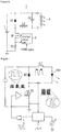
- the present embodiment is different from the first example in that the direct-current power source 1 includes an AC-DC converter and further the load voltage V1 of the LED module 4 is feed backed to the AC-DC converter. Meanwhile, other configurations are the same as those of the first embodiment, and accordingly explanations of the same components will be omitted by adding the same reference numerals.
- the LED lighting device includes: the step-down chopper circuit part 2, the control circuit part 3, and a voltage detection part 6 for detecting the load voltage V1 of the LED module 4 and feed backing the load voltage V1 to the direct-current power source 1.
- the direct-current power source 1 includes the AC-DC converter for converting an alternating-current output of a commercial alternating-current power source 5 into a direct-current voltage of a desired voltage value, and includes: an error amplifier 12 for comparing the load voltage V1 of the LED module 4 with the output voltage Vout and amplifying and outputting the error, and a control circuit 11 for controlling the switching element Q2 to be turned on and off in accordance with an output value of the error amplifier 12.
- the voltage detection part 6 detects the load voltage V1 of the LED module 4 and feed backs the load voltage V1 to the direct-current power source 1, and in the direct-current power source 1, the feedback controls is performed so that the output voltage Vout can be K times larger than the feed backed load voltage V1. Accordingly, in the same manner as that of the first example when 1 ⁇ K ⁇ 2.5 is set, the off period Toff where the optical output does not vary due to the change of the duty ratio of the PWM signal can be shortened, and consequently the optical output can be smoothly changed in the sweeping of the PWM signal.
- the load voltage V1 when the load voltage V1 is feed backed to the direct-current power source 1, a relationship between the output voltage Vout of the direct-current power source 1 and the load voltage V1 of the LED module 4 can be retained to be constant even in the case where the load voltage V1 caries, and consequently, the optical output variation more close to a linear-shape with respect to the PWM signal can be realized.
- the on-duty of the switching element Q1 is 1/K, and the more the K is close to 1, the more the illumination variation becomes smooth.
- ripples of 100Hz/120Hz appear in the output voltage Vout due to a capacity of an electrolytic capacitor C1 and the like, and thus the flicker of the optical output of the LED module 4 may occur due to interference between the ripples and a frequency of the PWM signal.
- Fig. 6 is a schematic circuit diagram showing another example of the LED lighting device according to the present embodiment, the illustrations of the AC-DC converter and the voltage detection part 6 in Fig. 5 are omitted.
- an electrolytic capacitor C2 is connected in parallel with the LED module 4, the ripples of the current flowing to the LED module 4 can be reduced by the electrolytic capacitor C2, and consequently the flicker of the optical output can be suppressed.
- the illumination fixture able to smoothly change the optical output in the sweeping of the PWM signal can be provided by using the LED lighting device according to the present embodiment.
- the direct-current power source 1 includes the AC-DC converter but may include a DC-DC converter.
- the step-down chopper circuit part 2 is provided on a low-voltage side of the direct-current power source 1; however, the step-down chopper circuit part 2 may be provided on a high-voltage side of the direct-current power source 1.
- the LED lighting device employing the LED as loads is explained as an example; however, the load is desired to be the solid light-emitting element, for example, may be an organic EL.
- the on/off of the switching element Q1 is controlled in accordance with the drive pulse in the on-period of the PWM signal (refer to Fig. 2 ); however, the on/off of the switching element Q1 may be controlled in accordance with the drive pulse in the off-period of the PWM signal. Meanwhile, in this case, it is required to set the length of the off-period of the PWM signal in accordance with the dimming level.
Landscapes
- Circuit Arrangement For Electric Light Sources In General (AREA)
Description
- The present invention relates to a solid light-emitting element lighting device and to an illumination fixture using the same.
- Conventionally, an LED lighting device for supplying lighting power to an LED illumination module is provided (for example, refer to JPT 2006-511078 and paragraphs [0015] to [0017] and
Fig. 7 to Fig. 9 ). As shown inFig. 7 , the LED lighting device includes: a control switch Q3 for being turned on and off in accordance with a dual signal including a low-frequency burst of high-frequency pulse, the control switch Q3 being connected to anLED illumination module 104 in series; an inductor L2 for accumulating energy when the control switch Q3 is turned on, the inductor similarly being connected to theLED illumination module 104 in series; and a diode D2 for regenerating the energy accumulated in the inductor L2 to theLED illumination module 104 at the turning-off of the control switch Q3. The above-mentioned dual signal is an AND output of a high-frequency drive pulse and a low-frequency PWM signal to the control switch Q3, an average current flowing to theLED illumination module 104 is varied by changing a duty ratio of the PWM signal, and thus a light intensity outputted from theLED illumination module 104 is changed (so-called burst dimming). -
US 2007/0188112 A1 shows a solid light-emitting element lighting device comprising: a series circuit of an inductor and a switching element that are connected between output terminals of a direct-current power source via a load; a diode for regenerating, during turning-off of the switching element, energy accumulated during turning-on of the switching element in the inductor to the load; and a control circuit part for controlling on and off of the switching element. The control circuit part includes a drive signal generation part for generating the drive signal whose pulse width varies in accordance with an amplitude of a load current. - In order to prevent an excessive current flowing through the load, the device according to
US 2007/0188112 A1 further contains a blocking means that blocks a PWM signal so that the drive signal is low if the current flowing through the load exceeds a preset value when the PWM signal is high. The current through the load is determined by measuring a shunt voltage that is subtracted from the high level voltage of the PWM signal and the difference is compared with a preset voltage value. -
WO 2010/046065 A1 proposes a lighting device for an LED module. A series circuit of an inductor and a switching element that are connected between output terminals of a direct-current power source via the LED module. A diode for regenerating, during turning-off of the switching element, energy accumulated during turning-on of the switching element in the inductor to the LED module is provided. A capacitor is connected parallel with the LED module to minimize ripples of the current flowing through the LED module. The switching element ist preferably switched when the current through the switching element is zero to avoid losses. - In the LED lighting device shown in above-mentioned JPT 2006-511078, the high-frequency drive pulse to the control switch Q3 is the AND output including the low-frequency PWM signal, and when an edge of the above-mentioned PWM signal is inputted during the turning-on of the control switch Q3, the drive pulse to the control switch Q3 becomes Low. Specifically, the on-period of the control switch Q3 is changed due to the variation of the low-frequency PWM signal, and accordingly an LED current, that is, an optical output of the
LED illumination module 104 varies. On the other hand, during the off-period of the control switch Q3, the regeneration current of the inductor L2 flows to theLED illumination module 104 via the diode D2; however, even when the above-mentioned PWM signal varies, the LED current does not change during the period. That is, despite the variation of the PWM signal, the optical output of theLED module 104 does not change. -
Fig. 8 is a time chart of the case where the control switch Q3 is operated in a critical mode (a mode in which the control switch Q3 is switched from being turned off to being turned on at timing when the current flowing to the inductor L2 becomes zero). As shown inFig. 8 , in the case where the PWM signal changed from the solid line to the broken line, that is, in the case where the on-period of the PWM signal becomes long, a load current I1 of theLED illumination module 104 will increase by one cycle of the drive signal (the broken line inFig. 8 ). In addition, since the larger a difference between an input voltage and an output voltage is, the more a slope of the current at the turning-on of the control switch Q3 becomes steep, in the case of obtaining the same output, the on-period will be short, and thus the off-period of the control switch Q3 is lengthened by the shortened on-period to extend the regeneration period (refer to the drive signal inFig. 8 ). - Accordingly, since the optical output does not vary during the off-period of the control switch Q3 even in the case of trying to smoothly change a dimming level, for example, by sweeping the duty of the above-mentioned PWM signal, the optical output to the duty variation will be stepwise as shown in
Fig. 9 . Then, the optical output difference of the one step is equivalent to the optical output of the one cycle of the high-frequency drive pulse for the control switch Q3, and accordingly the stepwise variation of the optical output can be watched. Specifically, since a variation rate of the optical output at the sweeping is large under a low light flux state, the stepwise variation will be more apparent. - As described above, in the case where the difference between the input voltage and the output voltage is large, the ratio of the period where the optical output does not vary in the sweeping of the PWM signal is large, and consequently there causes a problem that the optical output appears to vary in a stepwise fashion.
- The present invention is achieved in consideration of the above-mentioned problems, and a purpose of the present invention is to provide a solid light-emitting element lighting device and an illumination fixture using the same that are able to smoothly change the optical output in the sweeping of the PWM signal for dimming.
- A solid light-emitting element lighting device of the present invention includes the features of
claim 1. - In the solid light-emitting element lighting device, it is preferred that the control circuit part includes a zero current detection circuit for detection that a current flowing to the inductor becomes zero, and switches the switching element from being turned off to being turned on in synchronization with detection timing of the zero current detection circuit.
- Additionally, in the solid light-emitting element lighting device, it is preferred that the control circuit part switches the switching element to be turned on before the current flowing to the inductor during the turning-off of the switching element becomes zero.
- Moreover, in the solid light-emitting element lighting device, it is preferred that the direct-current power source includes an AC-DC converter or a DC-DC converter to which a detection result of the load voltage is feed backed and that controls an output voltage to be a voltage proportional to the detection result, and includes a voltage detection part for detecting the load voltage and feed backing the load voltage to the direct-current power source.
- Furthermore, in the solid light-emitting element lighting device, it is preferred that the direct-current power source includes the AC-DC converter, and a frequency of the PWM signal is set to 600Hz or multiples of 600Hz.
- An illumination fixture of the present invention includes: the solid light-emitting element lighting device according to any one of
claims 1 to 5; and a solid light-emitting element to which lighting power is supplied from the solid light-emitting element lighting device. - An effect to provide a solid light-emitting element lighting device and an illumination fixture using the same that are able to smoothly change the optical output in the sweeping of the PWM signal for dimming can be obtained.
-
- [
Fig. 1] Fig. 1 is a schematic circuit diagram showing an example LED lighting device. - [
Fig. 2] Fig. 2 is a time chart for explaining an operation of the above-mentioned device. - [
Fig. 3] Fig. 3 is a graph for explaining the operation of the above-mentioned device. - [
Fig. 4] Fig. 4 is a schematic circuit diagram showing another example of the above-mentioned LED lighting device. - [
Fig. 5] Fig. 5 is a schematic circuit diagram showing an LED lighting device according an embodiment of the invention. - [
Fig. 6] Fig. 6 is a schematic circuit diagram showing another example of the above-mentioned LED lighting device. - [
Fig. 7] Fig. 7 is a schematic circuit diagram showing a conventional LED lighting device. - [
Fig. 8] Fig. 8 is a time chart for explaining an operation of the above-mentioned device. - [
Fig. 9] Fig. 9 is a graph for explaining the operation of the above-mentioned device. - On the basis of drawings, embodiments of an illumination fixture using a LED lighting device will be explained below.
-
Fig. 1 is a schematic circuit view showing an LED lighting device (a solid light-light emitting device lighting device) according to a first example. The LED lighting device includes: a step-downchopper circuit part 2 for stepping down an output voltage of a direct-current power source 1 to a direct current of a desired voltage value; and acontrol circuit part 3 for controlling a switching element Q1 to be turned on and off, the switching element Q1 described later constituting the step-downchopper circuit part 2. In addition, an illumination fixture according to the present example includes: the LED lighting device; and a LED module (a solid light-emitting element, a load) 4 to which lighting power is supplied from the LED lighting device. Meanwhile, in the present embodiment, theLED module 4 includes three LEDs (light-emitting diodes); however, the number of LEDs is not limited to the present example and may be one, two, four or more. - The step-down
chopper circuit part 2 includes: a series circuit of an inductor L1 and the switching element Q1, the series circuit being connected between output terminals of the direct-current power source 1 via theLED module 4; and a diode D1 for regenerating energy during the turning-off of the switching element Q1, the energy being accumulated in the inductor L1 during the turning-on of the switching element Q1. - The
control circuit part 3 includes: astarter 32 for outputting a start-up signal to generate a drive pulse during stopping of oscillation at regular intervals; a zerocurrent detection circuit 31 for detecting that a current flowing to a secondary wiring N2 of the inductor L1 becomes zero; and a drivepulse generation part 34 for generating the drive pulse to turn on and off the switching element Q1. In addition, thecontrol circuit part 3 includes: adrive circuit 33 for driving the switching element Q1 in response to the drive pulse from the drivepulse generation part 34; acomparator 35 for outputting a reset signal to the drivepulse generation part 34 when a current flowing to the switching element Q1 reaches a reference value. - In the present example, the drive
pulse generation part 34 includes a RS flip-flop; to a set terminal of the RS flip-flop, an OR output of a detection signal of the zerocurrent detection circuit 31 and the start-up signal of thestarter 32 is inputted via anOR circuit 36, and an output of the drivepulse generation part 34 becomes High when the set signal is inputted. In addition, the output of the drivepulse generation part 34 becomes Low when the reset signal is inputted from thecomparator 35, and thus a high-frequency drive pulse where the High and Low are alternately repeated is outputted from the drivepulse generation part 34. - Additionally, to the
drive circuit 33, an AND output of the high-frequency drive pulse inputted from the drivepulse generation part 34 and the lower-frequency PWM signal than the drive pulse is inputted via anAND circuit 37, and thedrive circuit 33 controls the switching element Q1 to be turned on and off in accordance with the AND output. Here, the above-mentioned drive pulse changes the pulse width on the basis of amplitude of a load current flowing to theLED module 4, and the above-mentioned PWM signal changes the on-duty on the basis of a dimming level. Meanwhile, a resistance R1 inFig. 1 is a resistance for current detection to detect the current flowing to the switching element Q1. - Next, an operation of the LED lighting device will be explained. When the reset signal is inputted to the drive
pulse generation part 34 due to an output signal from thestarter 32 or the zerocurrent detection circuit 31 during a period where the above-mentioned PWM signal is High, the output of the drivepulse generation part 34 becomes High, the switching element Q1 is turned on via thedrive circuit 33, and thus a current flows to light theLED module 4. On this occasion, a temporal change of the load current I1 flowing to the switching element Q1 is shown as follows.
[Expression 1]
expression 1, Vout represents the output voltage of the direct-current source 1, V1 represents the load voltage of theLED module 4, t represents an elapsed time, L1 represents an impedance of the inductor, and a starting time of the turning-on of the switching element Q1 is t = 0. - When a voltage between both ends of the resistance R1 (that is, I1 × R1) reaches a reference voltage Vref, the output of the
comparator 35 is inverted, the reset signal is inputted to the drivepulse generation part 34, the output of the drivepulse generation part 34 becomes Low, and thus the switching element Q1 is turned off. When the switching element Q1 is turned off, the energy accumulated in the inductor L1 is regenerated to theLED module 4, and thus theLED module 4 is lighted by the regeneration current. On this occasion, the temporal change of the current I2 flowing to the inductor L1 is represented as follows.
[Expression 2]
expression 2, Ton represents the on-period of the switching element Q1 and Idp represents a peak current flowing to the inductor L1. - And, when the current I2 flowing to the inductor L1 during the turning-off of the switching element Q1 becomes zero, thereby inverting the current due to a function of the inductor L1, the electric charge charged in the switching element Q1 is discharged. As the result, the voltage between the drain and source of the switching element Q1 is decreased, and the voltage of the inductor L1 is inverted. The zero
current detection circuit 31 detects the voltage inverting and outputs the set signal to the drivepulse generation part 34, and thereby the switching element Q1 is turned on again at near zero of the current I2 flowing to the inductor L1. Then, the chopper operation is realized by repeating a series of the operations. Here, in the present example, the switching element Q1 is switched from being turned off to being turned on at timing when the current I2 flowing to the inductor L1 becomes zero, and the mode is referred to as a critical mode. - On the other hand, when the above-mentioned PWM signal becomes Low, it is stopped to input the drive pulse to the
drive circuit 33, and accordingly the oscillation is stopped during the period, that is, a state where theLED module 4 is lighted off is produced. Then, by varying the on-duty of the above-mentioned PWM signal, a ratio between a lighting-on state and the lighted-off state is changed, and consequently the output of theLED module 4 can be controlled. - Meanwhile, even if the above-mentioned PWM signal is varied during the off-period of the switching element Q1, the load current I1 flowing to the
LED module 4 does not change. That is, even when the on-duty of the PWM signal is varied, the optical output of theLED module 4 does not change. Here, the on-period Ton and on-period Toff of the switching element Q1 are represented as follows in accordance with expression (1) and expression (2).
[Expression 3]
[Expression 4]
- And, the on-duty Don of the switching element Q1 is represented as follows in accordance with expression (3) and expression (4).
[Expression 5]
- According to expression (5), it is found that the on-duty of the switching element Q1 is determined only by the output voltage Vout of the direct-
current power source 1 and the load voltage V1 of theLED module 4. - Here, when the output voltage Vout of the direct-
current power source 1 is defined as "Vout = K × V1", K = 1/Don is drawn from expression (5).Fig. 2 is a time chart for explaining the operation of the LED lighting device according to the present example, and shows a case of K = 1.2.
As will be understood in comparison withFig. 8 , since the off-period Toff of the switching element Q1 is very short in comparison with the on-period Ton, the load current I1 of theLED module 4 is slightly increased even when the PWM signal is varied, for example, from a solid line to a broken line. And accordingly the rapid change of the optical output can be suppressed. -
Fig. 3 shows change of the optical output to the duty ratio of the PWM signal, and a solid line b inFig. 3 shows the above-mentioned conventional LED lighting device, which corresponds to K = 10 in this case. A dashed line c inFig. 3 corresponds to K = 1.1, the optical output substantially continuously changes in accordance with the variation of the duty ratio, and thus the stepwise changing of the optical output can be reduced even in the extraordinary deep dimming level. Additionally, a broken line d inFig. 3 corresponds to K = 2.5, a period where the optical output is constant is approximately 60% on this occasion; however, the optical output variation is slower in comparison with the case of K = 10. In this case, the optical output appears to change in a stepwise fashion when theLED module 4 is directly looked; however, the change was in a level where the change cannot be recognized on an irradiation surface of the light as a flicker. Meanwhile, when K>2.5 is satisfied, the change is recognized on the above-mentioned irradiation surface as the flicker, and accordingly it is preferable to set the output voltage Vout of the direct-current power source 1 to be two and half times larger than the load voltage V1 of theLED module 4 or less. Additionally, in order to realize the step-down chopper operation, the lower limit of the output voltage Vout requires K>1, it is preferable to satisfy 1<K≤2.5. Moreover, considering the variation of the load voltage V1 due to a temperature characteristic of the LED and the like, it is more preferable to satisfy 1.2≤K≤2.5. - Next,
Fig. 4 is a schematic circuit diagram showing another example of the LED lighting device according to the present embodiment. In the example shown inFig. 1 , a drive pulse of the drivepulse generation part 34 and an AND output of the PWM signal are outputted to thedrive circuit 33 with use of the ANDcircuit 37; however, in the present example, a voltage superimposing the PWM signal on the voltage of the resistance R1 is compared with the reference voltage Vref, and the reset signal is outputted to the drivepulse generation part 34 in the case of exceeding the reference voltage Vref. Meanwhile, other configurations are the same as those ofFig. 1 , and accordingly the same numerals are given to the same components to omit the explanations. - According to the present configuration, a signal of the reference voltage Vref or more is inputted to the
comparator 35 when the PWM signal is Low, and thus the reset signal continues to be inputted to the drivepulse generation part 34. Accordingly, on this occasion, the drive pulse is not inputted to thedrive circuit 33, and the switching element Q1 is kept to be off. On the other hand, when the PWM signal is High, the output of the drivepulse generation part 34 becomes High due to the inputting of the output signal from thestarter 32 or the zerocurrent detection circuit 31 to turn on the switching element Q1 via thedrive circuit 33, in the same manner as that of the LED lighting device shown inFig. 1 . Then, when the load current I1 flowing to the switching element Q1 increases and the signal inputted to thecomparator 35 via the resistance R2 becomes the reference voltage Vref or more, thecomparator 35 outputs the reset signal, and accordingly the output of the drivepulse generation part 34 becomes Low to turn off the switching element Q1. Specifically, when the PWM signal is High, the switching element Q1 is controlled to be on and off due to the drive pulse from the drivepulse generation part 34 in the same manner as that of the LED lighting device shown inFig. 1 . In addition, according to the configuration, a universal IC for PFC (MC33262 manufactured by the ON Semiconductor Co., Ltd. and L6562 manufactured by STMicroelectronics Co., Ltd.) can be used as thecontrol circuit part 3, and consequently the number of parts can be reduced. - Thus, according to the present example, by setting the output voltage Vout of the direct-
current power source 1 to be larger than the load voltage V1 of theLED module 4 and to be 2.5 times as large as the load voltage V1 or less, the off period Toff where the optical output does not vary due to the change of the duty ratio of the above-mentioned PWM signal can be shortened, and consequently the optical output can be smoothly changed in the sweeping of the PWM signal. In addition, by switching the switching element Q1 to be turned on in synchronization with detection timing of the zerocurrent detection circuit 31, the on/off control of the switching element Q1 can be certainly performed. Moreover, an illumination fixture able to smoothly change the optical output in the sweeping of the PWM signal can be provided by using the LED lighting device according to the present embodiment. - Here, in the present example, the switching element Q1 is controlled in the critical mode; however, the switching element Q1 may be controlled in a sequential mode for switching the switching element Q1 to be turned on, for example, before the current I2 flowing to the inductor L1 in the turning-off of the switching element Q1 becomes zero (I2>0). Also in this case, by setting the output voltage Vout of the direct-
current power source 1 to be larger than the load voltage V1 of theLED module 4 and to be 2.5 times as large as the load voltage V1 or less, the optical output can be smoothly changed in the sweeping of the PWM signal, and additionally the on/off control of the switching element Q1 can be certainly performed. Meanwhile, in the case where the switching element Q1 is controlled in a non-sequential mode (an operation mode having a period where the current I2 flowing to the inductor L1 becomes zero), the off-period of the switching element Q1 becomes long, and accordingly the operation mode is disadvantageous with respect to the above-mentioned critical mode and sequential mode, but has an advantage that the change of the optical output can be smooth. - An embodiment of an illumination fixture using the LED lighting device will be explained on the basis of
Figs. 5 and6 . The present embodiment is different from the first example in that the direct-current power source 1 includes an AC-DC converter and further the load voltage V1 of theLED module 4 is feed backed to the AC-DC converter. Meanwhile, other configurations are the same as those of the first embodiment, and accordingly explanations of the same components will be omitted by adding the same reference numerals. - The LED lighting device according to the present embodiment includes: the step-down
chopper circuit part 2, thecontrol circuit part 3, and avoltage detection part 6 for detecting the load voltage V1 of theLED module 4 and feed backing the load voltage V1 to the direct-current power source 1. - The direct-
current power source 1 includes the AC-DC converter for converting an alternating-current output of a commercial alternating-current power source 5 into a direct-current voltage of a desired voltage value, and includes: anerror amplifier 12 for comparing the load voltage V1 of theLED module 4 with the output voltage Vout and amplifying and outputting the error, and acontrol circuit 11 for controlling the switching element Q2 to be turned on and off in accordance with an output value of theerror amplifier 12. - Here, in the present embodiment, the
voltage detection part 6 detects the load voltage V1 of theLED module 4 and feed backs the load voltage V1 to the direct-current power source 1, and in the direct-current power source 1, the feedback controls is performed so that the output voltage Vout can be K times larger than the feed backed load voltage V1. Accordingly, in the same manner as that of the first example when 1<K<2.5 is set, the off period Toff where the optical output does not vary due to the change of the duty ratio of the PWM signal can be shortened, and consequently the optical output can be smoothly changed in the sweeping of the PWM signal. In addition, as in the present embodiment, when the load voltage V1 is feed backed to the direct-current power source 1, a relationship between the output voltage Vout of the direct-current power source 1 and the load voltage V1 of theLED module 4 can be retained to be constant even in the case where the load voltage V1 caries, and consequently, the optical output variation more close to a linear-shape with respect to the PWM signal can be realized. Meanwhile, the on-duty of the switching element Q1 is 1/K, and the more the K is close to 1, the more the illumination variation becomes smooth. - Meanwhile, in the case of using the AC-DC converter as in the present embodiment, ripples of 100Hz/120Hz appear in the output voltage Vout due to a capacity of an electrolytic capacitor C1 and the like, and thus the flicker of the optical output of the
LED module 4 may occur due to interference between the ripples and a frequency of the PWM signal. In order to avoid the interference, it is preferable to set the frequency of the PWM signal to 600Hz or multiples of 600Hz, and consequently the interference of the ripples can be suppressed in both cases of 100Hz and 120Hz to allow obtaining substantially constant optical output where the flicker is suppressed. - In addition,
Fig. 6 is a schematic circuit diagram showing another example of the LED lighting device according to the present embodiment, the illustrations of the AC-DC converter and thevoltage detection part 6 inFig. 5 are omitted. In the example shown inFig. 6 , an electrolytic capacitor C2 is connected in parallel with theLED module 4, the ripples of the current flowing to theLED module 4 can be reduced by the electrolytic capacitor C2, and consequently the flicker of the optical output can be suppressed. Moreover, the illumination fixture able to smoothly change the optical output in the sweeping of the PWM signal can be provided by using the LED lighting device according to the present embodiment. - Here, in the present embodiment, the direct-
current power source 1 includes the AC-DC converter but may include a DC-DC converter. Additionally, in the present embodiment, the step-downchopper circuit part 2 is provided on a low-voltage side of the direct-current power source 1; however, the step-downchopper circuit part 2 may be provided on a high-voltage side of the direct-current power source 1. Moreover, in the above-mentioned first and second embodiments, the LED lighting device employing the LED as loads is explained as an example; however, the load is desired to be the solid light-emitting element, for example, may be an organic EL. Furthermore, in the above-mentioned first and second embodiments, the on/off of the switching element Q1 is controlled in accordance with the drive pulse in the on-period of the PWM signal (refer toFig. 2 ); however, the on/off of the switching element Q1 may be controlled in accordance with the drive pulse in the off-period of the PWM signal. Meanwhile, in this case, it is required to set the length of the off-period of the PWM signal in accordance with the dimming level. -
- 1
- Direct-current power source
- 3
- Control circuit part
- 4
- LED module (Solid light-emitting element and loads)
- 34
- Drive pulse generation part
- D1
- Diode
- L1
- Inductor
- Q1
- Switching element
Claims (5)
- A solid light-emitting element lighting device comprising:a direct-current power source (1), and a series circuit of an inductor (L1) and a switching element (Q1) that
are connected between output terminals of the direct-current power source (1) via a load (4);a diode (D1) for regenerating, during turning-off of the switching element (Q1) energy accumulated during turning-on of the switching element (Q1) in the inductor (L1) to the load (4);and a control circuit part (3) for controlling on and off of the switching element (Q1), whereinthe control circuit part (3) includes a drive signal generation part (34) for generating a drive signal whose pulse width varies in accordance with an amplitude of a load current (Il), and controls the on and off of the switching element (Q1) according to the drive signal in an on-period or an off-period of a PWM signal whose on-duty varies in accordance with a dimming level, the PWM signal being a lower frequency than the drive signal ; anda voltage detection part (6) for detecting the load voltage (V1) applied to the load (4) and
feeding back the load voltage (V1) to the direct-current power source (1) is provided;characterized in that the direct-current power source (1) includes an AC-DC converter or a DC-DC converter to which the detected load voltage (V1) is fed back and that controls the output voltage (Vout) to be K times larger than the detected load voltage (V1) according to wherein the the on-duty (Don) of the switching element (Q1) is
- The solid light-emitting element lighting device according to claim 1, wherein
the control circuit part (3) includes a zero current detection circuit (31) for detection that a current flowing to the inductor (L1) becomes zero, and switches the switching element (Q1) from being turned off to being turned on in synchronization with detection timing of the zero current detection circuit (31). - The solid light-emitting element lighting device according to claim 1, wherein
the control circuit part (3) switches the switching element (Q1) to be turned on before a current flowing to the inductor (L1) during the turning-off of the switching element (Q1) becomes zero. - The solid light-emitting element lighting device according to any one of claims 1 to 3, wherein
the direct-current power source (1) includes the AC-DC converter, and a frequency of the PWM signal is set to 600Hz or multiples of 600Hz. - An illumination fixture comprising: the solid light-emitting element lighting device according to any one of claims 1 to 4; and a solid light-emitting element to which lighting power is supplied from the solid light-emitting element lighting device.
Applications Claiming Priority (1)
| Application Number | Priority Date | Filing Date | Title |
|---|---|---|---|
| JP2011060866A JP5821023B2 (en) | 2011-03-18 | 2011-03-18 | Solid state light emitting device lighting device and lighting apparatus using the same |
Publications (2)
| Publication Number | Publication Date |
|---|---|
| EP2519079A1 EP2519079A1 (en) | 2012-10-31 |
| EP2519079B1 true EP2519079B1 (en) | 2017-11-22 |
Family
ID=46044310
Family Applications (1)
| Application Number | Title | Priority Date | Filing Date |
|---|---|---|---|
| EP12159970.8A Not-in-force EP2519079B1 (en) | 2011-03-18 | 2012-03-16 | Solid light-emitting element lighting device and illumination fixture using the same |
Country Status (3)
| Country | Link |
|---|---|
| EP (1) | EP2519079B1 (en) |
| JP (1) | JP5821023B2 (en) |
| CN (1) | CN102685977B (en) |
Families Citing this family (9)
| Publication number | Priority date | Publication date | Assignee | Title |
|---|---|---|---|---|
| JP6167400B2 (en) * | 2013-08-02 | 2017-07-26 | パナソニックIpマネジメント株式会社 | Lighting device, lighting fixture, lighting device design method, and lighting device manufacturing method |
| JP6493725B2 (en) | 2014-08-27 | 2019-04-03 | パナソニックIpマネジメント株式会社 | Lighting device and lighting apparatus |
| JP6315336B2 (en) | 2014-08-27 | 2018-04-25 | パナソニックIpマネジメント株式会社 | Lighting device and lighting apparatus |
| CN104467422B (en) * | 2014-12-22 | 2017-04-26 | 英飞特电子(杭州)股份有限公司 | Constant-current Buck converter and constant-current control circuit thereof |
| CN108243542B (en) * | 2016-12-26 | 2021-07-27 | 精工爱普生株式会社 | Light emission control circuit, light source device, and projection type image display device |
| EP3639623B1 (en) | 2017-06-12 | 2024-05-29 | Signify Holding B.V. | Method and apparatus for driving an led |
| CN107333358B (en) * | 2017-08-10 | 2023-09-22 | 浙江生辉照明有限公司 | Induction type bulb |
| CN109640433B (en) * | 2017-10-05 | 2023-03-31 | 精工爱普生株式会社 | Light emission control circuit, light source device, and projection type image display device |
| GB2587285B (en) * | 2018-07-13 | 2022-05-18 | Tridonic Gmbh & Co Kg | Method and device of controlling dimmable driver, dimmable driver |
Family Cites Families (8)
| Publication number | Priority date | Publication date | Assignee | Title |
|---|---|---|---|---|
| JP2767781B2 (en) * | 1993-09-17 | 1998-06-18 | 東光株式会社 | AC-DC converter |
| WO2001058218A1 (en) * | 2000-02-03 | 2001-08-09 | Koninklijke Philips Electronics N.V. | Supply assembly for a led lighting module |
| US7071762B2 (en) * | 2001-01-31 | 2006-07-04 | Koninklijke Philips Electronics N.V. | Supply assembly for a led lighting module |
| JP4796849B2 (en) * | 2006-01-12 | 2011-10-19 | 日立アプライアンス株式会社 | DC power supply, light-emitting diode power supply, and lighting device |
| KR100917623B1 (en) * | 2006-02-13 | 2009-09-17 | 삼성전자주식회사 | LED Driving Apparatus |
| CN101237190A (en) * | 2008-01-25 | 2008-08-06 | 魏其萃 | High-precision average output current control scheme for critical interrupted and continuous current mode of power current converter |
| JP2010040878A (en) * | 2008-08-06 | 2010-02-18 | Toshiba Lighting & Technology Corp | Lighting device for light-emitting diode |
| GB2476609B (en) * | 2008-10-20 | 2014-02-19 | Tridonic Ag | Operating circuit for light diodes |
-
2011
- 2011-03-18 JP JP2011060866A patent/JP5821023B2/en active Active
-
2012
- 2012-03-08 CN CN201210059376.0A patent/CN102685977B/en active Active
- 2012-03-16 EP EP12159970.8A patent/EP2519079B1/en not_active Not-in-force
Non-Patent Citations (1)
| Title |
|---|
| None * |
Also Published As
| Publication number | Publication date |
|---|---|
| JP5821023B2 (en) | 2015-11-24 |
| CN102685977B (en) | 2015-04-01 |
| JP2012199002A (en) | 2012-10-18 |
| EP2519079A1 (en) | 2012-10-31 |
| CN102685977A (en) | 2012-09-19 |
Similar Documents
| Publication | Publication Date | Title |
|---|---|---|
| EP2519079B1 (en) | Solid light-emitting element lighting device and illumination fixture using the same | |
| CN102695328B (en) | Lamp device and lighting apparatus | |
| EP2503846B1 (en) | Lighting device and illumination apparatus using the same | |
| JP5089193B2 (en) | Light emitting device | |
| US8698409B2 (en) | Lighting device and lighting fixture using the same | |
| TWI533746B (en) | Controller and method for dimming and light source driving circuit thereof | |
| US8203283B2 (en) | Light emitting diode (LED) arrangement with bypass driving | |
| JP5263503B2 (en) | Light emitting diode lighting device | |
| US20130278145A1 (en) | Circuits and methods for driving light sources | |
| US9078319B2 (en) | Conversion control circuit and converter thereof | |
| US8922130B2 (en) | Solid-state light-emitting element drive device, lighting system and lighting fixture | |
| JP2009277514A (en) | Led dimming lighting device, illumination device for vehicle, and luminaire | |
| TW201519695A (en) | Light source driving circuit, color temperature controller and method for controlling color temperature of light source | |
| KR101933823B1 (en) | A LED lighting device with the power supply equipped with a plurality of converters | |
| JP7425399B2 (en) | Power supplies and lighting equipment | |
| JP7273356B2 (en) | Lighting device and lighting device | |
| JP2012195252A (en) | Lighting device and lighting fixture using the lighting device | |
| JP2023079689A (en) | Lighting device and illuminating fixture |
Legal Events
| Date | Code | Title | Description |
|---|---|---|---|
| PUAI | Public reference made under article 153(3) epc to a published international application that has entered the european phase |
Free format text: ORIGINAL CODE: 0009012 |
|
| AK | Designated contracting states |
Kind code of ref document: A1 Designated state(s): AL AT BE BG CH CY CZ DE DK EE ES FI FR GB GR HR HU IE IS IT LI LT LU LV MC MK MT NL NO PL PT RO RS SE SI SK SM TR |
|
| AX | Request for extension of the european patent |
Extension state: BA ME |
|
| 17P | Request for examination filed |
Effective date: 20121119 |
|
| 17Q | First examination report despatched |
Effective date: 20141204 |
|
| RAP1 | Party data changed (applicant data changed or rights of an application transferred) |
Owner name: PANASONIC INTELLECTUAL PROPERTY MANAGEMENT CO., LT |
|
| GRAP | Despatch of communication of intention to grant a patent |
Free format text: ORIGINAL CODE: EPIDOSNIGR1 |
|
| STAA | Information on the status of an ep patent application or granted ep patent |
Free format text: STATUS: GRANT OF PATENT IS INTENDED |
|
| INTG | Intention to grant announced |
Effective date: 20170802 |
|
| RIN1 | Information on inventor provided before grant (corrected) |
Inventor name: IDO, SHIGERU Inventor name: NARUO, MASAHIRO |
|
| GRAJ | Information related to disapproval of communication of intention to grant by the applicant or resumption of examination proceedings by the epo deleted |
Free format text: ORIGINAL CODE: EPIDOSDIGR1 |
|
| STAA | Information on the status of an ep patent application or granted ep patent |
Free format text: STATUS: EXAMINATION IS IN PROGRESS |
|
| GRAR | Information related to intention to grant a patent recorded |
Free format text: ORIGINAL CODE: EPIDOSNIGR71 |
|
| GRAS | Grant fee paid |
Free format text: ORIGINAL CODE: EPIDOSNIGR3 |
|
| STAA | Information on the status of an ep patent application or granted ep patent |
Free format text: STATUS: GRANT OF PATENT IS INTENDED |
|
| GRAA | (expected) grant |
Free format text: ORIGINAL CODE: 0009210 |
|
| STAA | Information on the status of an ep patent application or granted ep patent |
Free format text: STATUS: THE PATENT HAS BEEN GRANTED |
|
| INTC | Intention to grant announced (deleted) | ||
| AK | Designated contracting states |
Kind code of ref document: B1 Designated state(s): AL AT BE BG CH CY CZ DE DK EE ES FI FR GB GR HR HU IE IS IT LI LT LU LV MC MK MT NL NO PL PT RO RS SE SI SK SM TR |
|
| INTG | Intention to grant announced |
Effective date: 20171017 |
|
| REG | Reference to a national code |
Ref country code: GB Ref legal event code: FG4D |
|
| REG | Reference to a national code |
Ref country code: CH Ref legal event code: EP |
|
| REG | Reference to a national code |
Ref country code: IE Ref legal event code: FG4D |
|
| REG | Reference to a national code |
Ref country code: AT Ref legal event code: REF Ref document number: 949517 Country of ref document: AT Kind code of ref document: T Effective date: 20171215 |
|
| REG | Reference to a national code |
Ref country code: DE Ref legal event code: R096 Ref document number: 602012040000 Country of ref document: DE |
|
| REG | Reference to a national code |
Ref country code: NL Ref legal event code: MP Effective date: 20171122 |
|
| REG | Reference to a national code |
Ref country code: LT Ref legal event code: MG4D |
|
| REG | Reference to a national code |
Ref country code: AT Ref legal event code: MK05 Ref document number: 949517 Country of ref document: AT Kind code of ref document: T Effective date: 20171122 |
|
| PG25 | Lapsed in a contracting state [announced via postgrant information from national office to epo] |
Ref country code: ES Free format text: LAPSE BECAUSE OF FAILURE TO SUBMIT A TRANSLATION OF THE DESCRIPTION OR TO PAY THE FEE WITHIN THE PRESCRIBED TIME-LIMIT Effective date: 20171122 Ref country code: NL Free format text: LAPSE BECAUSE OF FAILURE TO SUBMIT A TRANSLATION OF THE DESCRIPTION OR TO PAY THE FEE WITHIN THE PRESCRIBED TIME-LIMIT Effective date: 20171122 Ref country code: LT Free format text: LAPSE BECAUSE OF FAILURE TO SUBMIT A TRANSLATION OF THE DESCRIPTION OR TO PAY THE FEE WITHIN THE PRESCRIBED TIME-LIMIT Effective date: 20171122 Ref country code: NO Free format text: LAPSE BECAUSE OF FAILURE TO SUBMIT A TRANSLATION OF THE DESCRIPTION OR TO PAY THE FEE WITHIN THE PRESCRIBED TIME-LIMIT Effective date: 20180222 Ref country code: FI Free format text: LAPSE BECAUSE OF FAILURE TO SUBMIT A TRANSLATION OF THE DESCRIPTION OR TO PAY THE FEE WITHIN THE PRESCRIBED TIME-LIMIT Effective date: 20171122 Ref country code: SE Free format text: LAPSE BECAUSE OF FAILURE TO SUBMIT A TRANSLATION OF THE DESCRIPTION OR TO PAY THE FEE WITHIN THE PRESCRIBED TIME-LIMIT Effective date: 20171122 |
|
| PG25 | Lapsed in a contracting state [announced via postgrant information from national office to epo] |
Ref country code: RS Free format text: LAPSE BECAUSE OF FAILURE TO SUBMIT A TRANSLATION OF THE DESCRIPTION OR TO PAY THE FEE WITHIN THE PRESCRIBED TIME-LIMIT Effective date: 20171122 Ref country code: BG Free format text: LAPSE BECAUSE OF FAILURE TO SUBMIT A TRANSLATION OF THE DESCRIPTION OR TO PAY THE FEE WITHIN THE PRESCRIBED TIME-LIMIT Effective date: 20180222 Ref country code: GR Free format text: LAPSE BECAUSE OF FAILURE TO SUBMIT A TRANSLATION OF THE DESCRIPTION OR TO PAY THE FEE WITHIN THE PRESCRIBED TIME-LIMIT Effective date: 20180223 Ref country code: AT Free format text: LAPSE BECAUSE OF FAILURE TO SUBMIT A TRANSLATION OF THE DESCRIPTION OR TO PAY THE FEE WITHIN THE PRESCRIBED TIME-LIMIT Effective date: 20171122 Ref country code: LV Free format text: LAPSE BECAUSE OF FAILURE TO SUBMIT A TRANSLATION OF THE DESCRIPTION OR TO PAY THE FEE WITHIN THE PRESCRIBED TIME-LIMIT Effective date: 20171122 Ref country code: HR Free format text: LAPSE BECAUSE OF FAILURE TO SUBMIT A TRANSLATION OF THE DESCRIPTION OR TO PAY THE FEE WITHIN THE PRESCRIBED TIME-LIMIT Effective date: 20171122 |
|
| PG25 | Lapsed in a contracting state [announced via postgrant information from national office to epo] |
Ref country code: CZ Free format text: LAPSE BECAUSE OF FAILURE TO SUBMIT A TRANSLATION OF THE DESCRIPTION OR TO PAY THE FEE WITHIN THE PRESCRIBED TIME-LIMIT Effective date: 20171122 Ref country code: CY Free format text: LAPSE BECAUSE OF FAILURE TO SUBMIT A TRANSLATION OF THE DESCRIPTION OR TO PAY THE FEE WITHIN THE PRESCRIBED TIME-LIMIT Effective date: 20171122 Ref country code: EE Free format text: LAPSE BECAUSE OF FAILURE TO SUBMIT A TRANSLATION OF THE DESCRIPTION OR TO PAY THE FEE WITHIN THE PRESCRIBED TIME-LIMIT Effective date: 20171122 Ref country code: DK Free format text: LAPSE BECAUSE OF FAILURE TO SUBMIT A TRANSLATION OF THE DESCRIPTION OR TO PAY THE FEE WITHIN THE PRESCRIBED TIME-LIMIT Effective date: 20171122 Ref country code: SK Free format text: LAPSE BECAUSE OF FAILURE TO SUBMIT A TRANSLATION OF THE DESCRIPTION OR TO PAY THE FEE WITHIN THE PRESCRIBED TIME-LIMIT Effective date: 20171122 |
|
| REG | Reference to a national code |
Ref country code: DE Ref legal event code: R097 Ref document number: 602012040000 Country of ref document: DE |
|
| PG25 | Lapsed in a contracting state [announced via postgrant information from national office to epo] |
Ref country code: IT Free format text: LAPSE BECAUSE OF FAILURE TO SUBMIT A TRANSLATION OF THE DESCRIPTION OR TO PAY THE FEE WITHIN THE PRESCRIBED TIME-LIMIT Effective date: 20171122 Ref country code: SM Free format text: LAPSE BECAUSE OF FAILURE TO SUBMIT A TRANSLATION OF THE DESCRIPTION OR TO PAY THE FEE WITHIN THE PRESCRIBED TIME-LIMIT Effective date: 20171122 Ref country code: RO Free format text: LAPSE BECAUSE OF FAILURE TO SUBMIT A TRANSLATION OF THE DESCRIPTION OR TO PAY THE FEE WITHIN THE PRESCRIBED TIME-LIMIT Effective date: 20171122 Ref country code: PL Free format text: LAPSE BECAUSE OF FAILURE TO SUBMIT A TRANSLATION OF THE DESCRIPTION OR TO PAY THE FEE WITHIN THE PRESCRIBED TIME-LIMIT Effective date: 20171122 |
|
| PLBE | No opposition filed within time limit |
Free format text: ORIGINAL CODE: 0009261 |
|
| STAA | Information on the status of an ep patent application or granted ep patent |
Free format text: STATUS: NO OPPOSITION FILED WITHIN TIME LIMIT |
|
| 26N | No opposition filed |
Effective date: 20180823 |
|
| REG | Reference to a national code |
Ref country code: CH Ref legal event code: PL |
|
| GBPC | Gb: european patent ceased through non-payment of renewal fee |
Effective date: 20180316 |
|
| PG25 | Lapsed in a contracting state [announced via postgrant information from national office to epo] |
Ref country code: MC Free format text: LAPSE BECAUSE OF FAILURE TO SUBMIT A TRANSLATION OF THE DESCRIPTION OR TO PAY THE FEE WITHIN THE PRESCRIBED TIME-LIMIT Effective date: 20171122 Ref country code: SI Free format text: LAPSE BECAUSE OF FAILURE TO SUBMIT A TRANSLATION OF THE DESCRIPTION OR TO PAY THE FEE WITHIN THE PRESCRIBED TIME-LIMIT Effective date: 20171122 |
|
| REG | Reference to a national code |
Ref country code: BE Ref legal event code: MM Effective date: 20180331 |
|
| REG | Reference to a national code |
Ref country code: IE Ref legal event code: MM4A |
|
| PG25 | Lapsed in a contracting state [announced via postgrant information from national office to epo] |
Ref country code: LU Free format text: LAPSE BECAUSE OF NON-PAYMENT OF DUE FEES Effective date: 20180316 |
|
| PG25 | Lapsed in a contracting state [announced via postgrant information from national office to epo] |
Ref country code: IE Free format text: LAPSE BECAUSE OF NON-PAYMENT OF DUE FEES Effective date: 20180316 |
|
| PG25 | Lapsed in a contracting state [announced via postgrant information from national office to epo] |
Ref country code: BE Free format text: LAPSE BECAUSE OF NON-PAYMENT OF DUE FEES Effective date: 20180331 Ref country code: CH Free format text: LAPSE BECAUSE OF NON-PAYMENT OF DUE FEES Effective date: 20180331 Ref country code: LI Free format text: LAPSE BECAUSE OF NON-PAYMENT OF DUE FEES Effective date: 20180331 Ref country code: GB Free format text: LAPSE BECAUSE OF NON-PAYMENT OF DUE FEES Effective date: 20180316 |
|
| PG25 | Lapsed in a contracting state [announced via postgrant information from national office to epo] |
Ref country code: FR Free format text: LAPSE BECAUSE OF NON-PAYMENT OF DUE FEES Effective date: 20180331 |
|
| PGFP | Annual fee paid to national office [announced via postgrant information from national office to epo] |
Ref country code: DE Payment date: 20190430 Year of fee payment: 8 |
|
| REG | Reference to a national code |
Ref country code: DE Ref legal event code: R079 Ref document number: 602012040000 Country of ref document: DE Free format text: PREVIOUS MAIN CLASS: H05B0033080000 Ipc: H05B0045000000 |
|
| PG25 | Lapsed in a contracting state [announced via postgrant information from national office to epo] |
Ref country code: MT Free format text: LAPSE BECAUSE OF NON-PAYMENT OF DUE FEES Effective date: 20180316 |
|
| PG25 | Lapsed in a contracting state [announced via postgrant information from national office to epo] |
Ref country code: TR Free format text: LAPSE BECAUSE OF FAILURE TO SUBMIT A TRANSLATION OF THE DESCRIPTION OR TO PAY THE FEE WITHIN THE PRESCRIBED TIME-LIMIT Effective date: 20171122 |
|
| PG25 | Lapsed in a contracting state [announced via postgrant information from national office to epo] |
Ref country code: HU Free format text: LAPSE BECAUSE OF FAILURE TO SUBMIT A TRANSLATION OF THE DESCRIPTION OR TO PAY THE FEE WITHIN THE PRESCRIBED TIME-LIMIT; INVALID AB INITIO Effective date: 20120316 Ref country code: PT Free format text: LAPSE BECAUSE OF FAILURE TO SUBMIT A TRANSLATION OF THE DESCRIPTION OR TO PAY THE FEE WITHIN THE PRESCRIBED TIME-LIMIT Effective date: 20171122 |
|
| PG25 | Lapsed in a contracting state [announced via postgrant information from national office to epo] |
Ref country code: MK Free format text: LAPSE BECAUSE OF NON-PAYMENT OF DUE FEES Effective date: 20171122 |
|
| PG25 | Lapsed in a contracting state [announced via postgrant information from national office to epo] |
Ref country code: AL Free format text: LAPSE BECAUSE OF FAILURE TO SUBMIT A TRANSLATION OF THE DESCRIPTION OR TO PAY THE FEE WITHIN THE PRESCRIBED TIME-LIMIT Effective date: 20171122 Ref country code: IS Free format text: LAPSE BECAUSE OF FAILURE TO SUBMIT A TRANSLATION OF THE DESCRIPTION OR TO PAY THE FEE WITHIN THE PRESCRIBED TIME-LIMIT Effective date: 20180322 |
|
| REG | Reference to a national code |
Ref country code: DE Ref legal event code: R119 Ref document number: 602012040000 Country of ref document: DE |
|
| PG25 | Lapsed in a contracting state [announced via postgrant information from national office to epo] |
Ref country code: DE Free format text: LAPSE BECAUSE OF NON-PAYMENT OF DUE FEES Effective date: 20201001 |