EP2518820A1 - Line conversion structure and antenna using same - Google Patents
Line conversion structure and antenna using same Download PDFInfo
- Publication number
- EP2518820A1 EP2518820A1 EP10839294A EP10839294A EP2518820A1 EP 2518820 A1 EP2518820 A1 EP 2518820A1 EP 10839294 A EP10839294 A EP 10839294A EP 10839294 A EP10839294 A EP 10839294A EP 2518820 A1 EP2518820 A1 EP 2518820A1
- Authority
- EP
- European Patent Office
- Prior art keywords
- slot
- conductor
- ground
- line
- dielectric layer
- Prior art date
- Legal status (The legal status is an assumption and is not a legal conclusion. Google has not performed a legal analysis and makes no representation as to the accuracy of the status listed.)
- Withdrawn
Links
- 238000006243 chemical reaction Methods 0.000 title claims abstract description 100
- 239000004020 conductor Substances 0.000 claims abstract description 418
- 230000005540 biological transmission Effects 0.000 claims description 33
- 239000010410 layer Substances 0.000 description 236
- 238000012360 testing method Methods 0.000 description 96
- 238000004088 simulation Methods 0.000 description 60
- 230000009467 reduction Effects 0.000 description 17
- 230000000694 effects Effects 0.000 description 14
- 238000007747 plating Methods 0.000 description 13
- 229920005989 resin Polymers 0.000 description 12
- 239000011347 resin Substances 0.000 description 12
- 238000000034 method Methods 0.000 description 11
- 230000008878 coupling Effects 0.000 description 9
- 238000010168 coupling process Methods 0.000 description 9
- 238000005859 coupling reaction Methods 0.000 description 9
- 238000010586 diagram Methods 0.000 description 7
- 230000005672 electromagnetic field Effects 0.000 description 7
- PNEYBMLMFCGWSK-UHFFFAOYSA-N aluminium oxide Inorganic materials [O-2].[O-2].[O-2].[Al+3].[Al+3] PNEYBMLMFCGWSK-UHFFFAOYSA-N 0.000 description 6
- 229910052751 metal Inorganic materials 0.000 description 5
- 239000002184 metal Substances 0.000 description 5
- 238000000151 deposition Methods 0.000 description 4
- 239000000463 material Substances 0.000 description 4
- 238000007639 printing Methods 0.000 description 4
- 239000000919 ceramic Substances 0.000 description 3
- 229910010293 ceramic material Inorganic materials 0.000 description 3
- 229920000840 ethylene tetrafluoroethylene copolymer Polymers 0.000 description 3
- 239000011888 foil Substances 0.000 description 3
- 239000002241 glass-ceramic Substances 0.000 description 3
- 239000007788 liquid Substances 0.000 description 3
- 238000004519 manufacturing process Methods 0.000 description 3
- 230000008569 process Effects 0.000 description 3
- 239000004065 semiconductor Substances 0.000 description 3
- 230000001629 suppression Effects 0.000 description 3
- 229910000881 Cu alloy Inorganic materials 0.000 description 2
- 229910018487 Ni—Cr Inorganic materials 0.000 description 2
- 229910052581 Si3N4 Inorganic materials 0.000 description 2
- VYPSYNLAJGMNEJ-UHFFFAOYSA-N Silicium dioxide Chemical compound O=[Si]=O VYPSYNLAJGMNEJ-UHFFFAOYSA-N 0.000 description 2
- 229910045601 alloy Inorganic materials 0.000 description 2
- 239000000956 alloy Substances 0.000 description 2
- 238000004140 cleaning Methods 0.000 description 2
- 229920006026 co-polymeric resin Polymers 0.000 description 2
- 239000012141 concentrate Substances 0.000 description 2
- 229910052593 corundum Inorganic materials 0.000 description 2
- 238000009826 distribution Methods 0.000 description 2
- 239000003822 epoxy resin Substances 0.000 description 2
- 230000005284 excitation Effects 0.000 description 2
- 239000010408 film Substances 0.000 description 2
- 239000011521 glass Substances 0.000 description 2
- 239000006112 glass ceramic composition Substances 0.000 description 2
- 229910052737 gold Inorganic materials 0.000 description 2
- 230000002452 interceptive effect Effects 0.000 description 2
- 239000011229 interlayer Substances 0.000 description 2
- 238000010030 laminating Methods 0.000 description 2
- 238000003475 lamination Methods 0.000 description 2
- 229920000647 polyepoxide Polymers 0.000 description 2
- 229920001343 polytetrafluoroethylene Polymers 0.000 description 2
- 239000004810 polytetrafluoroethylene Substances 0.000 description 2
- HQVNEWCFYHHQES-UHFFFAOYSA-N silicon nitride Chemical compound N12[Si]34N5[Si]62N3[Si]51N64 HQVNEWCFYHHQES-UHFFFAOYSA-N 0.000 description 2
- 229910052709 silver Inorganic materials 0.000 description 2
- 230000007704 transition Effects 0.000 description 2
- 229910052721 tungsten Inorganic materials 0.000 description 2
- 229910001845 yogo sapphire Inorganic materials 0.000 description 2
- PIGFYZPCRLYGLF-UHFFFAOYSA-N Aluminum nitride Chemical compound [Al]#N PIGFYZPCRLYGLF-UHFFFAOYSA-N 0.000 description 1
- 229910017309 Mo—Mn Inorganic materials 0.000 description 1
- 239000004642 Polyimide Substances 0.000 description 1
- 238000009825 accumulation Methods 0.000 description 1
- 239000000853 adhesive Substances 0.000 description 1
- 230000001070 adhesive effect Effects 0.000 description 1
- 230000015572 biosynthetic process Effects 0.000 description 1
- 230000008859 change Effects 0.000 description 1
- 229910052681 coesite Inorganic materials 0.000 description 1
- 239000002131 composite material Substances 0.000 description 1
- 238000005260 corrosion Methods 0.000 description 1
- 230000007797 corrosion Effects 0.000 description 1
- 229910052906 cristobalite Inorganic materials 0.000 description 1
- 238000013461 design Methods 0.000 description 1
- 238000001035 drying Methods 0.000 description 1
- 238000001704 evaporation Methods 0.000 description 1
- 230000008020 evaporation Effects 0.000 description 1
- 230000002349 favourable effect Effects 0.000 description 1
- 238000010304 firing Methods 0.000 description 1
- NBVXSUQYWXRMNV-UHFFFAOYSA-N fluoromethane Chemical compound FC NBVXSUQYWXRMNV-UHFFFAOYSA-N 0.000 description 1
- LNEPOXFFQSENCJ-UHFFFAOYSA-N haloperidol Chemical compound C1CC(O)(C=2C=CC(Cl)=CC=2)CCN1CCCC(=O)C1=CC=C(F)C=C1 LNEPOXFFQSENCJ-UHFFFAOYSA-N 0.000 description 1
- 239000011256 inorganic filler Substances 0.000 description 1
- 229910003475 inorganic filler Inorganic materials 0.000 description 1
- 238000009413 insulation Methods 0.000 description 1
- 238000003754 machining Methods 0.000 description 1
- CPLXHLVBOLITMK-UHFFFAOYSA-N magnesium oxide Inorganic materials [Mg]=O CPLXHLVBOLITMK-UHFFFAOYSA-N 0.000 description 1
- 229910052750 molybdenum Inorganic materials 0.000 description 1
- 238000000465 moulding Methods 0.000 description 1
- 229920011301 perfluoro alkoxyl alkane Polymers 0.000 description 1
- 229920013653 perfluoroalkoxyethylene Polymers 0.000 description 1
- 229920001721 polyimide Polymers 0.000 description 1
- -1 polytetrafluoroethylene Polymers 0.000 description 1
- 238000003825 pressing Methods 0.000 description 1
- 238000012545 processing Methods 0.000 description 1
- 238000007650 screen-printing Methods 0.000 description 1
- 230000008054 signal transmission Effects 0.000 description 1
- 239000000377 silicon dioxide Substances 0.000 description 1
- 229910052682 stishovite Inorganic materials 0.000 description 1
- 238000003860 storage Methods 0.000 description 1
- BFKJFAAPBSQJPD-UHFFFAOYSA-N tetrafluoroethene Chemical group FC(F)=C(F)F BFKJFAAPBSQJPD-UHFFFAOYSA-N 0.000 description 1
- 239000010409 thin film Substances 0.000 description 1
- 238000012546 transfer Methods 0.000 description 1
- 229910052905 tridymite Inorganic materials 0.000 description 1
- WFKWXMTUELFFGS-UHFFFAOYSA-N tungsten Chemical compound [W] WFKWXMTUELFFGS-UHFFFAOYSA-N 0.000 description 1
- 239000010937 tungsten Substances 0.000 description 1
Images









Classifications
-
- H—ELECTRICITY
- H01—ELECTRIC ELEMENTS
- H01P—WAVEGUIDES; RESONATORS, LINES, OR OTHER DEVICES OF THE WAVEGUIDE TYPE
- H01P5/00—Coupling devices of the waveguide type
- H01P5/08—Coupling devices of the waveguide type for linking dissimilar lines or devices
- H01P5/10—Coupling devices of the waveguide type for linking dissimilar lines or devices for coupling balanced lines or devices with unbalanced lines or devices
- H01P5/1007—Microstrip transitions to Slotline or finline
-
- H—ELECTRICITY
- H01—ELECTRIC ELEMENTS
- H01P—WAVEGUIDES; RESONATORS, LINES, OR OTHER DEVICES OF THE WAVEGUIDE TYPE
- H01P5/00—Coupling devices of the waveguide type
- H01P5/08—Coupling devices of the waveguide type for linking dissimilar lines or devices
- H01P5/10—Coupling devices of the waveguide type for linking dissimilar lines or devices for coupling balanced lines or devices with unbalanced lines or devices
- H01P5/107—Hollow-waveguide/strip-line transitions
-
- H—ELECTRICITY
- H01—ELECTRIC ELEMENTS
- H01Q—ANTENNAS, i.e. RADIO AERIALS
- H01Q13/00—Waveguide horns or mouths; Slot antennas; Leaky-waveguide antennas; Equivalent structures causing radiation along the transmission path of a guided wave
- H01Q13/10—Resonant slot antennas
Definitions
- the present invention relates to a line conversion structure in which a high-frequency transmission line formed in a dielectric layer is converted into a slot line, and in particular to a line conversion structure suitable for interlayer connection in a transmission line, connection to an antenna, connection to a waveguide, or the like in a semiconductor element storage package or a wiring board that is preferable for housing or mounting semiconductor elements intended for high frequencies ranging from microwave to millimeter-wave frequency bands, and to an antenna using such a line conversion structure.
- high-frequency elements semiconductor elements for high frequencies (hereinafter simply referred to as "high-frequency elements") used in such an applied system or the like are housed/mounted, interlayer connection in a transmission line or connection to an antenna, for example, is in many cases established via a slot line.
- Patent Literature 1 A wiring board disclosed in Patent Literature 1 is known as an example of a wiring board using such transmission line connection via a slot line.
- a microstrip line configured in an upper dielectric layer and an output microstrip line configured in a lower dielectric layer are connected at high frequencies with electromagnetic coupling via a slot provided between the dielectric layers.
- the characteristic of the electromagnetic coupling between the microstrip lines and the slot in such a wiring board varies depending on a stub length and a slot length, the stub length being a length from an open end of each microstrip line to the center of the slot.
- the variation in the slot length is determined by only the variation in print dimensions and is thus relatively small.
- the variation in the stub length readily increases due to the variation in print position in forming the microstrip lines, the variation in print position in forming the slot, and layer-to-layer misalignment in laminating the upper and lower dielectric layers, which results in the problem that there is variation in the characteristic of the electromagnetic coupling between the microstrip lines and the slot.
- a wiring board disclosed in Patent Literature 2 is also known as an example of a line conversion structure in which a line for transmitting high frequencies is converted into a slot line.
- This example gives a wiring board for connecting a coplanar line to a dielectric waveguide via a slot formed in the same plane as the coplanar line.
- the variation in the stub length is relatively small because it depends only on the variation in print dimensions without experiencing the influence of the variation in print position and the layer-to-layer misalignment as described in the above case. Accordingly, the variation in the characteristic of the conversion from the coplanar line to the slot is reduced.
- a wiring board disclosed in Patent Literature 3 is known as an example of a line conversion structure in which a microstrip line is converted into a coplanar line.
- This example gives a wiring board in which the conversion into a coplanar line is achieved by, while reducing the width of a signal conductor of the microstrip line, forming a ground conductor on both sides of the signal conductor with a gap provided between the ground conductors and the signal conductor, and reducing these gaps so as to make the impedance constant.
- a line conversion structure is a line conversion structure for converting a high-frequency transmission line into a slot line.
- the high-frequency transmission line includes a dielectric layer, a signal conductor disposed on an upper surface of the dielectric layer, and a ground layer disposed on a lower surface of the dielectric layer.
- the slot line includes a slot ground conductor, a slot signal conductor, and a slot.
- the slot ground conductor is disposed on the upper surface of the dielectric layer and connected to the ground layer with a through conductor that passes through the dielectric layer.
- the slot signal conductor is disposed on the upper surface of the dielectric layer.
- the slot is disposed between the slot ground conductor and the slot signal conductor.
- the signal conductor of the high-frequency transmission line is orthogonal to the slot ground conductor and the slot, with a gap between the signal conductor and the slot ground conductor, and an end of the signal conductor is connected to the slot signal conductor.
- a length of a portion of the slot ground conductor, the portion being parallel to the signal conductor with the gap, is less than or equal to 0.25 time a wavelength of a signal transmitted through the high-frequency transmission line.
- An antenna according to an embodiment of the invention includes the above-described line conversion structure in which both end portions of the slot are closed, a lower dielectric layer, a lower ground layer, a first opening, a second opening, and a plurality of shield conductors.
- the lower dielectric layer is formed on the lower surface of the dielectric layer.
- the lower ground layer is formed on a lower surface of the lower dielectric layer.
- the first opening is formed in a portion of the ground layer that faces the slot.
- the second opening is formed in a portion of the lower ground layer that faces the slot.
- the plurality of shield conductors are configured to surround the first opening and the second opening in a plan view, and to connect the ground layer and the lower ground layer.
- the signal conductor of the high-frequency transmission line is orthogonal to the slot ground conductor and the slot, with a gap between the signal conductor and the slot ground conductor, an end of the signal conductor is connected to the slot signal conductor, and the length of the portion of the slot ground conductor, the portion being parallel to the signal conductor with the gap, is less than or equal to 0.25 times the wavelength of the signal transmitted through the high-frequency transmission line. Accordingly, in the portion where the signal conductor is orthogonal to the slot ground conductor with a gap between the signal conductor and the slot ground conductor, no transition to a coplanar line transmission mode occurs, and the high-frequency transmission line can be converted directly into the slot line. This also produces no resonance, thus achieving a line conversion structure with a small loss in conversion.
- the antenna according to the embodiment of the invention includes the line conversion structure of the above embodiment of the invention, in which both end portions of the slot are closed, the lower dielectric layer, the lower ground layer, the first opening, the second opening, and the plurality of shield conductors.
- signals that have been transmitted through the high-frequency transmission line are stored efficiently in the slot line as signal energy, and of the lower dielectric layer disposed on the underside of the slot, a portion that is surrounded by the shield conductors functions as a dielectric matching unit that achieves high-frequency matching between the slot and a space located on the underside of the lower dielectric layer. Accordingly, it is possible to emit signals through the first opening and the second opening to the space with a small loss (high efficiency).
- a microstrip line 1 serving as a high-frequency transmission line, a dielectric layer 2, a lower dielectric layer 2a, a signal conductor 3, a ground layer 4, a first opening 4a, a slot line 5, through conductors 6, ground-reinforcing conductors 6a, upper ground-reinforcing conductors 6b, a slot ground conductor 7, a slot signal conductor 8, a slot 9, a slot pattern conductor 9a, an upper dielectric layer 10 or 16, an upper ground layer 11 or 17, an output signal conductor 12, an output microstrip line 13, and a strip line 18 serving as a high-frequency transmission line are shown in Figs.
- FIG. 1A to 1D 2A to 2C, 3A to 3C, 4A to 4C, and 5A to 5C .
- the dielectric layer 2, the lower dielectric layer 2a, and the upper dielectric layer 10 or 16 are shown in a see-through manner in Figs. 1A to 5C .
- the dashed dotted line in Fig. 1B indicates a center line of the slot 9 in the widthwise direction.
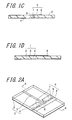
- Figs. 1A to 1D are schematic diagrams for illustrating an example of the line conversion structure according to the embodiment of the invention, Fig. 1A being a perspective view, Fig. 1B being a plan view, Fig. 1C being a cross-sectional view taken along the line A-A indicated in Fig. 1A , and Fig. 1D being a cross-sectional view taken along the line B-B indicated in Fig. 1A .
- the microstrip line 1 includes the dielectric layer 2, the signal conductor 3 disposed on an upper surface of the dielectric layer 2, and the ground layer 4 disposed on a lower surface of the dielectric layer 2 as in the example shown in Figs. 1A to 1D .
- the slot line 5 includes the slot ground conductor 7, the slot signal conductor 8, and the slot 9.
- the slot ground conductor 7 is disposed on the upper surface of the dielectric layer 2 and connected to the ground layer 4 with the through conductors 6 that pass through the dielectric layer 2.
- the slot signal conductor 8 is disposed on the upper surface of the dielectric layer 2.
- the slot 9 is disposed between the slot ground conductor 7 and the slot signal conductor 8.
- the signal conductor 3 of the microstrip line 1 is orthogonal to the slot ground conductor 7 and the slot 9, with a gap between the signal conductor 3 and the slot ground conductor 7, and one end of the signal conductor 3 is connected to the slot signal conductor 8.
- a stub length (which is indicated by ML in Fig. 1B , and in the example, half the width of the slot 9) that is a factor of the characteristic of conversion to the slot line 5 is not affected by a shift in print position and layer-to-layer misalignment during manufacture and depends only on the variation in print dimensions.
- the length of a portion of the slot ground conductor 7 (indicated by L in Fig. 1B ), the portion being parallel to the signal conductor 3 with a gap, is less than or equal to 0.25 times the wavelength of signals transmitted through the microstrip line 1. Accordingly, in a portion where the signal conductor 3 is orthogonal to the slot ground conductor 7 with a gap between the signal conductor 3 and the slot ground conductor 7, no transition to a coplanar line transmission mode occurs, and the microstrip line 1 can be converted directly into the slot line 5. This also produces no resonance, thus achieving a line conversion structure with a small loss in conversion.
- a distance (indicated by D in Fig. 1B ) between the signal conductor 3 and a through conductor 6 that is located closest to the portion of the slot ground conductor 7, the portion being parallel to the signal conductor 3 with a gap in between, is less than or equal to 0.13 times the wavelength of signals transmitted through the microstrip line 1
- the distance from the ground layer 4 located immediately under the signal conductor 3 of the microstrip line 1 via that through conductor 6 to the slot ground conductor 7 is sufficiently short. This allows the ground potential of the microstrip line 1 to be transmitted to the slot ground conductor 7 without delay, thus further reducing the loss in conversion from the microstrip line 1 to the slot line 5.
- Figs. 2A to 2C are schematic diagrams for illustrating another example of the line conversion structure according to the embodiment of the invention, Fig. 2A being a perspective view, Fig. 2B being a plan view, and Fig. 2C being a cross-sectional view taken along the line A-A indicated in Fig. 2A .
- the slot ground conductor 7 has a greater width and the through conductors 6 that connect the slot ground conductor 7 and the ground layer 4 have a greater diameter than in the example shown in Figs. 1A to 1D .
- a length L of only the portion of the slot ground conductor 7, the portion being parallel to the signal conductor 3 with a gap is made less than or equal to 0.25 times the wavelength of signals transmitted through the microstrip line 1.
- the width of the portion of the slot ground conductor 7 which portion is farther from the gap is greater than the width of the portion of the slot ground conductor 7 which portion is parallel to the signal conductor 3 with the gap in between.
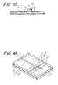
- Figs. 3A to 3C are schematic diagrams for illustrating still another example of the line conversion structure according to the embodiment of the invention, Fig. 3A being a perspective view, Fig. 3B being a plan view, and Fig. 3C being a cross-sectional view taken along the line A-A indicated in Fig. 3B . As in the example shown in Figs.
- an upper ground layer 11 is formed via an upper dielectric layer 10 on the dielectric layer 2 so as to cover a portion of the signal line 3 which portion is orthogonal to the slot line 5 and a gap therebetween, as well as a portion of the slot line 5 between the gap and the slot signal conductor 8, that is, to cover a line conversion unit.
- the line conversion unit in the line conversion structure of the embodiment is a portion where an electromagnetic field mode of signals transmitted through a microstrip line 1 is converted directly into an electromagnetic field mode of signals transmitted through the slot line 5.
- the electromagnetic field mode of that portion is thus more complex than the electromagnetic field mode of signals transmitted through a simple transmission line, and the line conversion unit has a structure susceptible to the influence of the emission to the outside or the incidence from the outside.
- covering the line conversion unit with the upper ground layer 11 achieves an effective reduction in the influence of the emission to the outside or the incidence from the outside.
- the upper ground layer 11 is formed only over the line conversion unit in the example shown in Figs. 3A to 3C , it is preferable that the upper ground layer 11 to be formed is larger than the line conversion unit in a plan view because this further enhances the above-described shield effect, and in the case of creating a wiring board or the like that includes the line conversion structure of the embodiment, allows the line conversion unit to be reliably covered even if there is somewhat of a shift in the position of the upper ground layer 11. Furthermore, if the entire upper surface of the dielectric layer 2 is covered with the upper ground layer 11 via the upper dielectric layer 10, the line conversion unit is completely shielded from above and below by the upper ground layer 11 located above and the ground layer 4 located below.
- multiple through conductors 6 may be provided in a line in the lengthwise direction of a slot ground conductor 7 (in a direction away from the gap). By doing so, it is possible to allow the through conductors 6 to pass through the dielectric layer 2, and thus suppress the incidence of noise from the outside to a slot 9 and the line conversion unit.
- a slot pattern conductor 9a is disposed on the upper surface of the dielectric layer 2 so as to close at least one end portion of the slot 9, it is possible to change the direction of signal transmission to the desired direction. For example, if the slot pattern conductor 9a is disposed so as to close only one end portion of the slot 9 as in the example shown in Figs. 2A to 2C , signals will be totally reflected at that closed end portion and transmitted to the other end portion of the slot 9. Thus, signals transmitted through the microstrip line 1 can be transmitted toward the desired one end portion of the slot 9.
- Figs. 4A to 4C are schematic diagrams for illustrating still another example of the line conversion structure according to the embodiment of the invention, Fig. 4A being a perspective view, Fig. 4B being a plan view, and Fig. 4C being a cross-sectional view taken along the line A-A indicated in Fig. 4A . If two slot pattern conductors 9a are disposed so as to close both end portions of a slot 9 as in the example shown in Figs.
- signals transmitted through a microstrip line 1 are temporarily stored in a slot line 5 as energy and transmitted, for example through a first opening 4a of a ground layer 4 formed on a lower surface of a dielectric layer 2, to another transmission line such as an output microstrip line 13 configured by the ground layer 4, a lower dielectric layer 2a formed therebelow, and an output signal conductor 12 formed on a lower surface of the lower dielectric layer 2a, or to an antenna, a waveguide, or the like that is disposed in a direction vertical to the slot.
- signals can be transmitted via the slot line 5 to an external element with electromagnetic coupling.
- Figs. 5A to 5C are schematic diagrams for illustrating still another example of the line conversion structure according to the embodiment of the invention, Fig. 5A being a plan view, Fig. 5B being a cross-sectional view taken along the line A-A indicated in Fig. 5A , and Fig. 5C being a cross-sectional view taken along the line B-B indicated in Fig. 5A .
- a strip line 18 serving as a high-frequency transmission line is converted into a slot line 5.
- Figs. 5A being a plan view
- Fig. 5B being a cross-sectional view taken along the line A-A indicated in Fig. 5A
- Fig. 5C being a cross-sectional view taken along the line B-B indicated in Fig. 5A .
- a strip line 18 serving as a high-frequency transmission line is converted into a slot line 5.
- Figs. 5A to 5C are schematic diagrams for illustrating still another example of the line conversion structure according to the embodiment of
- the strip line 18 includes an upper dielectric layer 16, an upper ground layer 17 disposed on an upper surface of the upper dielectric layer 16, a dielectric layer 2, a signal conductor 3 disposed on an upper surface of the dielectric layer 2, and a ground layer 4 disposed on a lower surface of the dielectric layer 2.
- the slot line 5 includes a slot ground conductor 7, a slot signal conductor 8, and a slot 9.
- the slot ground conductor 7 is disposed on the upper surface of the dielectric layer 2 and connected to the ground layer 4 with through conductors 6 that pass through the dielectric layer 2.
- the slot signal conductor 8 is disposed on the upper surface of the dielectric layer 2.
- the slot 9 is disposed between the slot ground conductor 7 and the slot signal conductor 8.
- the signal conductor 3 of the strip line 18 is orthogonal to the slot ground conductor 7 and the slot 9, with a gap provided between the signal conductor 3 and the slot ground conductor 7, and the end of the signal conductor 3 is connected to the slot signal conductor 8.
- slot pattern conductors 9a are disposed on the upper surface of the dielectric layer 2 so as to close both end portions of the slot 9.
- the length of a portion of each slot pattern conductor 9a, the portion being perpendicular to the signal conductor 3 (slot pattern width SW), is less than or equal to 0.25 times the wavelength of signals transmitted through the strip line 18.
- a ground-reinforcing conductor 6a that passes through the dielectric layer 2 and connects the slot ground conductor 7 and the ground layer 4 is formed in a region that extends from each end portion of the slot 9 in a direction away from the signal conductor 3 and ranges within 0.25 times the wavelength of signals transmitted through the strip line 18.
- the ground-reinforcing conductors 6a are provided such that clearance G between the ground-reinforcing conductors 6a and the ends of the slot 9 is less than or equal to 0.25 times the wavelength of signals transmitted through the strip line 18.
- the upper ground layer 17 enables suppression of signal emissions from above to the outside, thus suppressing a reduction in gain in the case where the line conversion structure is used in an antenna.
- upper ground-reinforcing conductors 6b that pass through the upper dielectric layer 16 and connect the slot ground conductor 7 and the upper ground layer 17.
- the provision of the upper ground-reinforcing conductors 6b in this way enables the potential at the end portions of the slot 9 on the slot ground conductor 7 side to be closer to the ground potential, thus further suppressing a reduction in gain.
- signals transmitted through the strip line 18 are temporarily stored in the slot line 5 as energy and transmitted, for example through a first opening 4a of the ground layer 4 formed on the lower surface of the dielectric layer 2, to another transmission line such as an output microstrip line 13 configured by the ground layer 4, a lower dielectric layer 2a formed therebelow, and an output signal conductor 12 formed on the lower surface of the lower dielectric layer 2a, or to an antenna, a waveguide, or the like that is disposed in a direction vertical to the slot 9.
- signals can be transmitted via the slot line 5 to an external element with electromagnetic coupling.
- a low-loss antenna can be configured.
- Figs. 6A to 6C are schematic diagrams for illustrating an example of an antenna according to an embodiment of the invention, Fig. 6A being a plan view, Fig. 6B being a cross-sectional view taken along the line A-A indicated in Fig. 6A , and Fig. 6C being a bottom view.
- a lower ground layer 14, a second opening 14a formed in the lower ground layer 14, and shield conductors 15 are shown in Figs. 6A to 6C , and other reference numerals denote components that are the same as those shown in Figs. 1A to 5C .
- the dielectric layer 2 and the lower dielectric layer 2a are shown in a see-through manner in Figs. 6A to 6C , as in Figs. 1A to 5C .
- the antenna in the example shown in Figs. 6A to 6C includes a line conversion structure having one of the configurations shown in Figs. 1A to 4C , in which both end portions of the slot 9 are closed, the lower dielectric layer 2a, the lower ground layer 14, the first opening 4a, the second opening 14a, and the plurality of shield conductors 15.
- the lower dielectric layer 2a is formed on the lower surface of the dielectric layer 2.
- the lower ground layer 14 is formed on the lower surface of the lower dielectric layer 2a.
- the first opening 4a is formed in a portion of the ground layer 4 that faces the slot 9.
- the second opening 14a is formed in a portion of the lower ground layer 14 that faces the slot 9.
- the plurality of shield conductors 15 are configured to surround the first opening 4a and the second opening 14a in a plan view, and connect the ground layer 4 and the lower ground layer 14. With the antenna configured in this way, signals transmitted through the microstrip line 1 is efficiently stored in the slot line 5 as signal energy, and out of the lower dielectric layer 2a that is disposed on the underside of the slot 9, the portion surrounded by the shield conductors 15 functions as a dielectric matching unit that achieves high-frequency matching between the slot 9 and a space below the lower dielectric layer 2a. It is thus possible to emit signals through the first opening 4a and the second opening 14a into the space with a small loss (high efficiency).
- the antenna will also achieve a smaller loss (higher efficiency).
- a loss in conversion from the microstrip line 1 to the slot line 5 is further reduced if the length (indicated by L in Fig. 1B ) of a portion of the slot ground conductor 7, the portion being parallel to the signal conductor 3 with a gap, is less than or equal to 0.25 times the wavelength of signals transmitted through the microstrip line 1 and if the distance (indicated by D in Fig.
- the antenna with such a configuration can efficiently emit high-frequency signals. Furthermore, with the antenna in the example shown in Figs. 6A to 6C , if an upper ground layer 11 is formed on the dielectric layer 2 via the upper dielectric layer 10 so as to cover a portion of the signal conductor 3, the portion being orthogonal to the slot line 5, the gap, and a portion of the slot line 5 between the gap and the slot signal conductor 8, that is, to cover the line conversion unit, as in the example shown in Figs.
- the antenna with such a configuration will be a lower-loss (more highly efficient) antenna, or a noise-resistant antenna.
- the antenna with such a configuration is a more highly efficient antenna that is capable of suppressing the occurrence of unnecessary resonance in the dielectric matching unit due to a disturbed electromagnetic field mode.
- the thickness of the lower dielectric layer 2a is set to one fourth the wavelength of signals in the lower dielectric layer 2a, so that the portion of the lower dielectric layer 2a that is surrounded by the shield conductors 15 functions as a dielectric matching unit that achieves impedance matching between the slot 9 and a space below the lower dielectric layer 2a into which signals are to be emitted. Since the wavelength of signals in the lower dielectric layer 2a varies depending on the frequency of signals transmitted through the microstrip line 1 and the effective dielectric constant of the lower dielectric layer 2a, the thickness of the lower dielectric layer 2a is set in accordance therewith.
- the plurality of shield conductors 15 are formed in the lower dielectric layer 2a and arranged so as to surround the first opening 4a and the second opening 14a in a plan view. Each of the shield conductors 15 connects the ground layer 4 and the lower ground layer 14.
- the shield conductors 15 are preferably arranged in close proximity outside the second opening. Since signals that have passed through the first opening 4a pass through the portion surrounded by the shield conductors 15, if a portion of the lower ground layer 14 that is located inside the shield conductors 15 is made smaller, it is possible to suppress interference with signal emissions in that portion. More preferably, the shield conductors 15 may be arranged adjacently outside the second opening 14a. In this case, the lower ground layer 14 will not interfere with signal emissions because there is almost no lower ground layer 14 inside the shield conductors 15.
- the distances between the plurality of shield conductors 15 are preferably less than or equal to one fourth the wavelength of signals transmitted through the dielectric matching unit, so as to avoid leakage of high-frequency signals from the gaps between the adjacent shield conductors 15.
- the slot 9, the first opening 4a, and the second opening 14a are disposed so as to face one another, i.e., to overlap one another in a plan view.
- the first opening 4a is larger than the slot 9, and the first opening 4a and the slot 9 are disposed so as to make their centers coincide.
- the second opening 14a is larger than the first opening 4a, and the first opening 4a and the second opening 14a are disposed so as to make their centers coincide.
- Such dimensions and disposition of the slot 9, the first opening 4a, and the second opening 14a enable signals to be favorably emitted from the slot 9 through the first opening 4a and the second opening 14a into the space thereunder.
- the first opening 4a has a shorter length than the second opening 14a in the direction parallel to the signal conductor 3.
- a magnetic field of unnecessary resonance in the dielectric matching unit is likely to occur along the outer periphery of the dielectric matching unit (a region close to the shield conductors 15), and a magnetic field of unnecessary resonance occurs as a result of excitation caused by a magnetic field occurring around the signal conductor 3, that is, a magnetic field occurring in a direction perpendicular to the signal conductor 3 in a plan view. For this reason, a magnetic field of unnecessary resonance is likely to occur in a portion on the outer periphery of the dielectric matching unit that extends in the direction perpendicular to the signal conductor 3.
- the ground layer 4 is between the portion where a magnetic field of unnecessary resonance is likely to occur and the signal conductor 3, and the ground layer 4 can serve as a shield against a magnetic field occurring around the signal conductor 3. It is thus possible to suppress the occurrence of a magnetic field of unnecessary resonance. Since a magnetic field of unnecessary resonance is likely to concentrate in a region that ranges within one fourth the distance between the shield conductors 15 and the center of the dielectric matching unit from the shield conductors 15, it is preferable that the length of the first opening 4a in the direction parallel to the signal conductor 3 (indicated by OL1 in Fig.
- the first opening 4a and the second opening 14a are disposed so as to make their centers coincide, and the length OL1 of the first opening 4a in the direction parallel to the signal conductor 3 is made shorter than half the length OL2 of the second opening 14a in the direction parallel to the signal conductor 3, a portion of the ground layer 4 around the first opening 4a is located on the region where a magnetic field of unnecessary resonance is likely to concentrate in the dielectric matching unit. This portion serves as an effective shield against a magnetic field occurring around the signal conductor 3, thus improving the effect of suppressing the occurrence of unnecessary resonance in the dielectric matching unit.
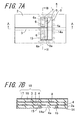
- Figs. 7A to 7C are schematic diagrams for illustrating another example of the antenna according to the embodiment of the invention, Fig. 7A being a plan view, Fig. 7B being a cross-sectional view taken along the line A-A indicated in Fig. 7A , and Fig. 7C being a cross-sectional view taken along the line B-B indicated in Fig. 7A .
- the dielectric layer 2, the lower dielectric layer 2a, and the upper dielectric layer 16 are shown in a see-through manner in Figs. 7A to 7C , as in Figs. 1A to 6C .
- the antenna in the example shown in Figs. 7A to 7C is configured in the same manner as the antenna shown in Figs.
- the antenna in the example shown in Figs. 7A to 7C includes the line conversion structure shown in Figs. 5A to 5C in which both end portions of the slot 9 are closed, the lower dielectric layer 2a, the lower ground layer 14, the first opening 4a, the second opening 14a, and the plurality of shield conductors 15.
- the lower dielectric layer 2a is formed on the lower surface of the dielectric layer 2.
- the lower ground layer 14 is formed on the lower surface of the lower dielectric layer 2a.
- the first opening 4a is formed in a portion of the ground layer 4 that faces the slot 9.
- the second opening 14a is formed in a portion of the lower ground layer 14 that faces the slot 9.
- the plurality of shield conductors 15 are arranged so as to surround the first opening 4a and the second opening 14a in a plan view, and connect the ground layer 4 and the lower ground layer 14.
- the portion surrounded by the shield conductors 15 functions as a dielectric matching unit that achieves high-frequency matching between the slot 9 and the space located below the lower dielectric layer 2a. It is thus possible to emit signals through the first opening 4a and the second opening 14a into the space with a small loss (high efficiency).
- the line conversion structure provided in the antenna is a structure as described above that is capable of suppressing a loss, the antenna can also suppress a reduction in gain.
- the dielectric layer 2, the upper dielectric layer 10 or 16, and the lower dielectric layer 2a are made of ceramics, an organic resin, or a composite of these two.
- the ceramics include ceramic materials such as an alumina (Al 2 O 3 ) sintered compact, an aluminum nitride (AlN) sintered compact, and a silicon nitride (Si 3 N 4 ) sintered compact, glass materials, and glass ceramic materials made of a complex of glass and an inorganic filler such as Al 2 O 3 , SiO 2 , or MgO.
- organic resins examples include fluorocarbon resins such as tetrafluoroethylene resins (polytetrafluoroethylene (PTFE)), ethylene-tetrafluoroethylene copolymer resins (ethylene-tetrafluoroethylene copolymer resin (ETFE)), and tetrafluoroethylene-perfluoroalkoxy ethylene copolymer resins (tetrafluoroethylene-perfluoroalkyl vinyl ether copolymer resins (PFA)), epoxy resins, glass-epoxy resins, and polyimide.
- fluorocarbon resins such as tetrafluoroethylene resins (polytetrafluoroethylene (PTFE)), ethylene-tetrafluoroethylene copolymer resins (ethylene-tetrafluoroethylene copolymer resin (ETFE)), and tetrafluoroethylene-perfluoroalkoxy ethylene copolymer resins (tetrafluoroethylene-perfluor
- a glass ceramic material that is capable of being co-fired with a conductor material made of a low-resistance metal such as Au, Ag, or Cu that is capable of transmitting high-frequency signals.
- the thickness of the dielectric layer 2 made of these materials is set according to the frequency to be used or the application, for example.
- the signal conductor 3, the ground layer 4, the slot ground conductor 7, the slot signal conductor 8, the slot pattern conductor(s) 9a, the upper ground layer 11 or 17, and the lower ground layer 14 are formed of a metalized layer that is made primarily of a metal such as W, Mo, Mo-Mn, Au, Ag, or Cu.
- these conductors and layers are formed of a metal layer formed by a thick-film printing method, various types of thin-film forming methods, a plating method, a foil transfer method, or the like, or formed of a layer configured by forming a plating layer on such a metal layer, examples of which include a Cu layer, a Cr-Cu alloy layer, a layer configured by depositing a Ni plating layer and a Au plating layer on a Cr-Cu alloy layer, a layer configured by depositing a Ni-Cr alloy layer and a Au plating layer on a TaN layer, a layer configured by depositing a Pt layer and a Au plating layer on a Ti layer, and a layer configured by depositing a Pt layer and a Au plating layer on a Ni-Cr alloy layer.
- the thicknesses and widths thereof are set according to the frequency of high-frequency signals to be transmitted or the application, for example.
- a known method may be used to form the signal conductor 3, the ground layer 4, the slot ground conductor 7, the slot signal conductor 8, the slot pattern conductor(s) 9a, the upper ground layer 11 or 17, and the lower ground layer 14.
- the dielectric layer 2 is made of glass ceramics
- green sheets of glass ceramics to be formed into the dielectric layer 2 are prepared first and then conductor patterns for the signal conductor 3, the ground layer 4, the slot ground conductor 7, the slot signal conductor 8, the slot pattern conductor(s) 9a, the upper ground layer 11 or 17, and the lower ground layer 14 are formed by applying conductor pastes such as Ag in a predetermined shape on the green sheets by printing using a screen printing technique.
- the signal conductor 3, the slot ground conductor 7, the slot signal conductor 8, and the slot pattern conductor(s) 9a are formed on the same green sheet at the same time.
- the green sheets with the conductor patterns having formed thereon are, for example, overlaid and bonded to one another by pressing so as to create a laminated body, which is then shaped by undergoing firing at 850 to 1000°C.
- films of plating such as Ni plating and Au plating are formed over the conductors exposed to the outer surface.
- the dielectric layer 2 is made of an organic resin material, for example, the signal conductor 3, the ground layer 4, the slot ground conductor 7, the slot signal conductor 8, the slot pattern conductor(s) 9a, the upper ground layer 11 or 17, and the lower ground layer 14 are formed by transferring, to organic resin sheets, Cu foils that have been processed into the shapes of the conductor patterns for these conductors and layers, and laminating and bonding the organic resin sheets, on which the Cu foils have been transferred, with an adhesive.
- organic resin sheets Cu foils that have been processed into the shapes of the conductor patterns for these conductors and layers, and laminating and bonding the organic resin sheets, on which the Cu foils have been transferred, with an adhesive.
- the through conductors 6, the ground-reinforcing conductors 6a, and the upper ground-reinforcing conductors 6b can be formed by, for example prior to the formation of the conductor patterns for the signal conductor 3, the ground layer 4, the slot ground conductor 7, the slot signal conductor 8, the slot pattern conductor(s) 9a, the upper ground layer 11 or 17, and the lower ground layer 14 in the aforementioned manufacturing method, forming through holes in green sheets in advance by metal molding or laser machining and filling the through holes with a similar conductor paste using a print process or the like.
- the dielectric layer 2 is made of an organic resin
- organic resin sheets are used instead of green sheets, and through conductors may be formed in through holes by printing or plating of a conductor paste.
- the shield conductors 15 may also be formed in the same manner as the through conductors 6, the ground-reinforcing conductors 6a, and the upper ground-reinforcing conductors 6b.
- a loss in conversion from the microstrip line 1 to the slot line 5 was estimated by simulating a loss caused during processing in which a signal inputted from the microstrip line 1 was output to the output microstrip line 13 on the lower surface of the dielectric layer 2.
- the first opening 4a for coupling the slot line 5 and the output microstrip line 13 was provided in the ground layer 4 inside the dielectric layer 2.
- the dielectric layer 2 was made of alumina
- the relative dielectric constant was set to 8.6
- the conductivity of the conductors was set to 6.6 ⁇ 10 6 (S/m)
- the signal frequency was set to 60 GHz.
- the thicknesses of the dielectric layer 2 and the lower dielectric layer 2a were set to 0.15 mm, and in order to set the impedance of the microstrip line 1 and the output microstrip line 13 to 50 Q, the widths of the signal conductor 3 and the output signal conductor 12 were set to 0.14 mm.
- the effective dielectric constant of the microstrip line 1 and the output microstrip line 13 was 6.3, and the wavelength of the signals at 60 GHz was 2.0 mm.
- the diameter of the through conductors 6 was set to 0.1 mm.
- the width of the slot 9 (the distance between the slot ground conductor 7 and the slot signal conductor 8) was set to 0.1 mm, and the length SL was set to 1.4 mm.
- the stub length ML of the output microstrip line 13 was set to 0.4 mm.
- the first opening 4a was assumed to have the shape of a rectangle of 1.8 mm ⁇ 0.35 mm, and was disposed so that the slot 9 was located in the center of the first opening 4a when viewed from above.
- the length L of the portion of the slot ground conductor 7 that was parallel to the signal conductor 3 with a gap in between was set to 0.25 times (0.5 mm) the wavelength of signals transmitted through the microstrip line 1, and the distance D between the signal conductor 3 and the through conductor 6 was set to 0.13 times (0.26 mm) the signal wavelength.
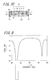
- Fig. 8 is a graph showing the frequency characteristics of the loss caused between the microstrip line 1 and the output microstrip line 13 of the simulation model, the vertical axis indicating the loss and the horizontal axis the frequency. It can be seen from Fig. 8 that signals were transmitted in the range of approximately 50 to 70 GHz, and favorable electromagnetic coupling between the microstrip line 1 and the output microstrip line 13 was observed in the 60 GHz band, which indicates that the conversion from the microstrip line 1 into the slot line 5 was made favorably.
- the loss at 60 GHz was 1.1 dB.
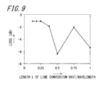
- Fig. 9 is a graph showing a relationship between the loss and the parallel length L at 60 GHz.
- the parallel length L shown was normalized in accordance with the wavelength of 60 GHz signals transmitted through the microstrip line 1 (in the form of a ratio of the parallel length L to the wavelength). It can be seen from Fig.
- the loss was small, approximately 1.1 dB, if the parallel length L was less than or equal to 0.25 times the wavelength, but the loss increased sharply if the parallel length L exceeded 0.25 times the wavelength.
- the loss was in particular great for the parallel length L being 0.5 times the wavelength, which was due to the influence of resonance. Although there was no influence of resonance if the parallel length L was 0.75 times the wavelength, the loss in this case was approximately 2.1 dB, which was greater by the order of 1 dB than that for the parallel length L being less than or equal to 0.25 times the wavelength.
- Fig. 10 is a graph showing a relationship between the loss and the distance D between the signal conductor 3 and the through conductor 6 at 60 GHz.
- the distance D between the signal conductor 3 and the through conductor 6 shown was normalized in accordance with the wavelength of 60 GHz signals transmitted through the microstrip line 1 (in the form of a ratio of the distance D to the wavelength). It can be seen from Fig. 10 that the loss was small, approximately 1.1 dB, if the distance D was less than or equal to 0.13 times the wavelength, but the loss increased sharply if the distance D exceeds 0.13 times the wavelength. The loss was in particular great for the distance D being 0.25 times the wavelength, which was due to the influence of resonance as described above. Similarly, if the distance D was 0.25n times (n being a positive integer), the loss would increase due to the influence of resonance.
- the loss in this case was approximately 2.1 dB, which was greater by the order of 1 dB than that for the distance D being less than or equal to 0.13 times the wavelength. This was considered because of a loss caused by an increase in the length of a transmission path when the potential of the ground layer 4 immediately below the signal conductor 3 of the microstrip line 1 was transmitted to the slot ground conductor 7 via the through conductors 6.
- the bandwidth of the antenna was estimated from the reflection characteristics of signals that were inputted from the microstrip line 1.
- the first opening 4a for coupling the slot line 5 and the dielectric matching unit was provided in the ground layer 4 on the lower surface of the dielectric layer 2.
- the relative dielectric constant was set to 8.6
- the conductivity of the conductors was set to 6.6 ⁇ 10 6 (S/m)
- the signal frequency was set to 60 GHz.
- the thickness of the dielectric layer 2 was set to 0.15 mm and the thickness of the lower dielectric layer 2a to 0.4 mm, and in order to set the impedance of the microstrip line 1 to 50 Q, the width of the signal conductor 3 was set to 0.14 mm.
- the diameters of the through conductors 6 and the shield conductors 15 were set to 0.1 mm.
- the width of the slot 9 (the distance between the slot ground conductor 7 and the slot signal conductor 8) was set to 0.1 mm, and the length SL was set to 1.4 mm.
- the first opening 4a was assumed to have the shape of a rectangle of 1.8 mm ⁇ 0.35 mm, and was disposed so that the slot 9 was located in the center of the first opening 4a when viewed from above.
- the shield conductors 15 were arranged at 0.3 mm pitch so that their center positions were located on the sides of a rectangle of 3.6 mm ⁇ 1.5 mm.
- the second opening 14a was assumed to have the shape of a rectangle of 3.6 mm ⁇ 1.5 mm.
- the rectangle that connected the shield conductors 15 and the second opening 14a were disposed so as to make their centers coincide with the center of the first opening 4a.
- Fig. 11 is a graph showing a frequency characteristic of the reflection of high-frequency signals to be inputted from the microstrip line 1 of the simulation model, the vertical axis indicating the reflection and the horizontal axis the frequency. It can be seen from Fig. 11 that the reflection was small, -10 dB or less, in the range of approximately 57 to 75GHz, which indicated that the antenna emitted high-frequency signals into the space over a wide band.
- the first opening 4a for coupling the slot line 5 and the dielectric matching unit was provided in the ground layer 4 on the lower surface of the dielectric layer 2.
- the relative dielectric constant was set to 9.2
- the conductivity of the conductors assumed to be metalized with tungsten was set to 6.6 ⁇ 10 6 (S/m)
- the signal frequency was set to 60 GHz.
- the thicknesses of the upper dielectric layer 16 and the dielectric layer 2 were set to 0.125 mm
- the thickness of the lower dielectric layer 2a was set to 0.4 mm
- the width of the signal conductor 3 of the strip line 18 was set to 0.1 mm.
- the gap between the slot ground conductor 7 and the signal conductor 3 was set to 0.1 mm.
- the diameters of the through conductors 6 and the shield conductors 15 were set to 0.1 mm, and the distance D between the through conductor 6 and the signal conductor 3 was set to 0.23 mm.
- the width of the slot 9 (the distance between the slot ground conductor 7 and the slot signal conductor 8) was set to 0.1 mm, and the length SL was set to 0.8 mm.
- the width of the slot signal conductor 8 was set to 0.205 mm.
- the two slot pattern conductors 9a were configured on the upper surface of the dielectric layer 2 so as to close both end portions of the slot 9, and the length of the portions of the slot pattern conductors 9a that were perpendicular to the signal conductor 3 (slot pattern width SW) was set to 0.35 times (0.577 mm) the wavelength of signals transmitted through the strip line 18. Note that, in Test Case 1, the simulations were conducted on the assumption that neither ground-reinforcing conductors 6a nor the upper ground-reinforcing conductors 6b were formed.
- Test Case 2 simulations were conducted in the same manner as in Test Case 1, with the exception that the length of the portions of the slot pattern conductors 9a that were perpendicular to the signal conductor 3 (slot pattern width SW) was set to 0.3 times (0.495 mm) the wavelength of signals transmitted through the strip line 18.
- Test Case 3 simulations were conducted in the same manner as in Test Case 1, with the exception that the length of the portions of the slot pattern conductors 9a that were perpendicular to the signal conductor 3 (slot pattern width SW) was set to 0.25 times (0.412 mm) the wavelength of signals transmitted through the strip line 18.
- Test Case 4 simulations were conducted in the same manner as in Test Case 1, with the exception that the length of the portions of the slot pattern conductors 9a that were perpendicular to the signal conductor 3 (slot pattern width SW) was set to 0.2 times (0.33 mm) the wavelength of signals transmitted through the strip line 18.
- Test Case 5 simulations were conducted in the same manner as in Test Case 1, with the exception that the length of the portions of the slot pattern conductors 9a that were perpendicular to the signal conductor 3 (slot pattern width SW) was set to 0.15 times (0.247 mm) the wavelength of signals transmitted through the strip line 18.
- Fig. 12 is a graph showing the relationship between the gain of the antenna and the slot pattern width in the case where no ground-reinforcing conductors are formed.
- the vertical axis indicates the gain (dBi), and the horizontal axis indicates the slot pattern width with respect to the wavelength.
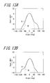
- Figs. 13A to 13C are graphs showing the simulation results for the gain of the antenna in Test Cases 1, 3, and 5.
- Fig. 13A shows the simulation results for Test Case 1, Fig. 13B for Test Case 3, and Fig.
- the vertical axis indicating the gain (dBi) and the horizontal axis indicating the angle (deg).
- the solid line A indicates the gain of the antenna in a plane that is parallel to the signal conductor 3 and perpendicular to the dielectric layer 2
- the broken line B indicates the gain of the antenna in a plane that is perpendicular to the signal conductor 3 and perpendicular to the dielectric layer 2.
- Test Case 1 0.35 0.577 5.3 Test Case 2 0.3 0.495 5.2 Test Case 3 0.25 0.412 3.5 Test Case 4 0.2 0.33 2.9 Test Case 5 0.15 0.247 1.8
- Test Case 6 simulations were conducted in the same manner as in Test Case 1, with the exception that the length of the portions of the slot pattern conductors 9a that were perpendicular to the signal conductor 3 (slot pattern width SW) was set to 0.25 times (0.412 mm) the wavelength of signals transmitted through the strip line 18, and the ground-reinforcing conductors 6a were disposed corresponding to the respective end portions of the slot 9 at positions that were spaced 0.25 times the wavelength of signals transmitted through the strip line 18 from the respective end portions of the slot 9 in directions away from the signal conductor 3 (that is, the clearance between the conductors and the end portions of the slot 9 was 0.25 times the wavelength). Note that in Test Case 6, the simulations were conducted on the assumption that no upper ground-reinforcing conductors 6b were formed.
- Test Case 7 simulations were conducted in the same manner as in Test Case 6, with the exception that the clearance between the ground-reinforcing conductors 6a and the end portions of the slot 9 was set to 0.125 times the wavelength.
- Test Case 8 simulations were conducted in the same manner as in Test Case 6, with the exception that the clearance between the ground-reinforcing conductors 6a and the end portions of the slot 9 was set to 0 times the wavelength, that is, the center positions of the ground-reinforcing conductors 6a were made coincide with the positions of the end portions of the slot 9.
- Test Case 9 simulations were conducted in the same manner as in Test Case 6, with the exception that the length of the portions of the slot pattern conductors 9a that were perpendicular to the signal conductor 3 (slot pattern width SW) was set to 0.15 times (0.247 mm) the wavelength of signals transmitted through the strip line 18, and the clearance between the ground-reinforcing conductors 6a and the end portions of the slot 9 was set to 0.15 times the wavelength.
- Test Case 10 simulations were conducted in the same manner as in Test Case 6, with the exception that the length of the portions of the slot pattern conductors 9a that were perpendicular to the signal conductor 3 (slot pattern width SW) was set to 0.15 times (0.247 mm) the wavelength of signals transmitted through the strip line 18, and the clearance between the ground-reinforcing conductors 6a and the end portions of the slot 9 was set to 0 times the wavelength, that is, the center positions of the ground-reinforcing conductors 6a were made coincide with the positions of the end portions of the slot 9.
- slot pattern width SW 0.15 times (0.247 mm) the wavelength of signals transmitted through the strip line 18
- the clearance between the ground-reinforcing conductors 6a and the end portions of the slot 9 was set to 0 times the wavelength, that is, the center positions of the ground-reinforcing conductors 6a were made coincide with the positions of the end portions of the slot 9.
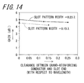
- Fig. 14 is a graph showing the relationship between the gain of the antenna and the clearance between the ground-reinforcing conductors and the end portions of the slot.
- the vertical axis indicates the gain (dBi)
- the horizontal axis indicates the clearance between the ground-reinforcing conductors and the end portions of the slot with respect to the wavelength.
- ⁇ denotes the wavelength of signals transmitted through the strip line 18.
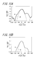
- Figs. 15A to 15C are graphs showing the simulation results for the gain of the antenna in Test Cases 6, 7, and 8.
- Fig. 15A shows the simulation results for Test Case 6, Fig. 15B for Test Case 7, and Fig. 15C for Test Case 8, the vertical axis indicating the gain (dBi) and the horizontal axis the angle (deg).
- the solid line A indicates the gain of the antenna in a plane that is parallel to the signal conductor 3 and perpendicular to the dielectric layer 2
- the broken line B indicates the gain of the antenna in a plane that is perpendicular to the signal conductor 3 and perpendicular to the dielectric layer 2.
- Test Case 6 0.25 0.25 4.6 Test Case 7 0.25 0.125 4.7 Test Case 8 0.25 0 5 Test Case 9 0.15 0.15 4.2 Test Case 10 0.15 0 4.5
- Test Case 11 simulations were conducted in the same manner as in Test Case 1, with the exception that the length of the portions of the slot pattern conductors 9a that were perpendicular to the signal conductor 3 (slot pattern width SW) was set to 0.25 times (0.412 mm) the wavelength of signals transmitted through the strip line 18, and the ground-reinforcing conductors 6a were provided on the extension of the signal conductor 3 so that the ground-reinforcing conductors 6a connected the slot signal conductor 8 and the ground layer 4.
- Fig. 16 is a graph showing the simulation results for the gain of the antenna in Test Case 11.
- the vertical axis indicates the gain (dBi), and the horizontal axis the angle (deg).
- the solid line A indicates the gain of the antenna in a plane that is parallel to the signal conductor 3 and perpendicular to the dielectric layer 2
- the broken line B indicates the gain of the antenna in a plane that is perpendicular to the signal conductor 3 and perpendicular to the dielectric layer 2. It can be seen from Fig. 16 that the effect of suppressing a reduction in gain was not obtained if the ground-reinforcing conductors 6a were provided so as to connect the slot signal conductor 8 and the ground layer 4.
- Test Case 12 simulations were conducted in the same manner as in Test Case 1, with the exception that the length of the portions of the slot pattern conductors 9a that were perpendicular to the signal conductor 3 (slot pattern width SW) was set to 0.15 times (0.247 mm) the wavelength of signals transmitted through the strip line 18, and a ground-reinforcing conductor 6a was disposed corresponding to only one end portion of the slot 9 at a position that was spaced 0.15 times the wavelength of signals transmitted through the strip line 18 from the one end portion of the slot 9 in a direction away from the signal conductor 3 (that is, the clearance between the conductor and the one end of the slot 9 was 0.15 times the wavelength).
- Test Case 13 simulations were conducted in the same manner as in Test Case 1, with the exception that the length of the portions of the slot pattern conductors 9a that were perpendicular to the signal conductor 3 (slot pattern width SW) was set to 0.15 times (0.247 mm) the wavelength of signals transmitted through the strip line 18, and the two ground-reinforcing conductors 6a were disposed at positions, specifically, at the position spaced 0.15 times the signal wavelength from one end portion of the slot 9 (i.e., the clearance between the conductor and the end of the slot 9 was 0.15 times the wavelength) and at the position spaced 0 times the signal wavelength from the other end portion of the slot 9 (i.e., the center position of the ground-reinforcing conductor 6a was made coincide with the position of the end portion of the slot 9).
- the positions where the two ground-reinforcing conductors 6a were disposed were asymmetrical with respect to the signal conductor 3.
- Table 4 Slot Patten Width with respect to Wavelength Clearance between Ground-Reinforcing Conductor and One End portion of Slot Clearance between Ground-Reinforcing Conductor and Other End Portion of Slot Gain (times) (times) (dBi) Test Case 13 0.15 0.15 0 2.8 Test Case 5 0.15 - - 1.8 Test case 9 0,15 0.15 0.15 4.2
- Test Case 14 simulations were conducted in the same manner as in Test Case 1, with the exception that the length of the portions of the slot pattern conductors 9a that were perpendicular to the signal conductor 3 (slot pattern width SW) was set to 0.15 times (0.247 mm) the wavelength of signals transmitted through the strip line 18, the ground-reinforcing conductors 6a were disposed corresponding to the respective end portions of the slot 9 at positions spaced 0.15 times the signal wavelength from the end portions of the slot 9 in directions away from the signal conductor 3 (i.e., the clearance between the conductors and the end portions of the slot 9 was 0.15 times the wavelength), and the upper ground-reinforcing conductors 6b were disposed corresponding to the respective end portions of the slot 9 at positions spaced 0.15 times the signal wavelength from the end portions of the slot 9 in directions away from the signal conductor 3 (i.e., the clearance between the conductors and the end portions of the slot 9 was 0.15 times the wavelength).
- Test Case 15 simulations were conducted in the same manner as in Test Case 14, with the exception that the upper ground-reinforcing conductors 6b were disposed corresponding to the respective end portions of the slot 9 at positions spaced 0 times the signal wavelength from the end portions of the slot 9 in directions away from the signal conductor 3 (i.e., the center positions of the upper ground-reinforcing conductors 6b were made coincide with the positions of the ends of the slot 9).
- the upper ground-reinforcing conductors 6b were disposed at positions that were shifted from the ground-reinforcing conductors 6a.
- Test Case 14 0.15 0.15 0.15 4.9
- Test Case 15 0.15 0.15 0 4.4
- Test Case 5 0.15 - - 1.8
- Test case 9 0.15 0.15 - 4.2
Landscapes
- Waveguide Aerials (AREA)
- Waveguides (AREA)
Abstract
Description
- The present invention relates to a line conversion structure in which a high-frequency transmission line formed in a dielectric layer is converted into a slot line, and in particular to a line conversion structure suitable for interlayer connection in a transmission line, connection to an antenna, connection to a waveguide, or the like in a semiconductor element storage package or a wiring board that is preferable for housing or mounting semiconductor elements intended for high frequencies ranging from microwave to millimeter-wave frequency bands, and to an antenna using such a line conversion structure.
- With the arrival of the advanced information age in recent years, utilization of radio waves ranging from the microwave frequency band of 1 to 30 GHz to even the millimeter-wave frequency band of 30 to 300 GHz for information transmission is being considered. For example, an applied system such as a domestic high-speed wireless transmission system (wireless personal area network (PAN)) using 60 GHz has now been proposed.
- Conventionally, with a wiring board in/on which semiconductor elements for high frequencies (hereinafter simply referred to as "high-frequency elements") used in such an applied system or the like are housed/mounted, interlayer connection in a transmission line or connection to an antenna, for example, is in many cases established via a slot line.
- A wiring board disclosed in
Patent Literature 1 is known as an example of a wiring board using such transmission line connection via a slot line. In this wiring board, a microstrip line configured in an upper dielectric layer and an output microstrip line configured in a lower dielectric layer are connected at high frequencies with electromagnetic coupling via a slot provided between the dielectric layers. - The characteristic of the electromagnetic coupling between the microstrip lines and the slot in such a wiring board varies depending on a stub length and a slot length, the stub length being a length from an open end of each microstrip line to the center of the slot. In the case where such a wiring board is manufactured using a printing or lamination technique, the variation in the slot length is determined by only the variation in print dimensions and is thus relatively small. On the other hand, the variation in the stub length readily increases due to the variation in print position in forming the microstrip lines, the variation in print position in forming the slot, and layer-to-layer misalignment in laminating the upper and lower dielectric layers, which results in the problem that there is variation in the characteristic of the electromagnetic coupling between the microstrip lines and the slot.
- A wiring board disclosed in
Patent Literature 2 is also known as an example of a line conversion structure in which a line for transmitting high frequencies is converted into a slot line. This example gives a wiring board for connecting a coplanar line to a dielectric waveguide via a slot formed in the same plane as the coplanar line. In this case, since the coplanar line and the slot are formed in the same plane, the variation in the stub length is relatively small because it depends only on the variation in print dimensions without experiencing the influence of the variation in print position and the layer-to-layer misalignment as described in the above case. Accordingly, the variation in the characteristic of the conversion from the coplanar line to the slot is reduced. - Furthermore, a wiring board disclosed in
Patent Literature 3 is known as an example of a line conversion structure in which a microstrip line is converted into a coplanar line. This example gives a wiring board in which the conversion into a coplanar line is achieved by, while reducing the width of a signal conductor of the microstrip line, forming a ground conductor on both sides of the signal conductor with a gap provided between the ground conductors and the signal conductor, and reducing these gaps so as to make the impedance constant. With such a wiring board, it is not easy to prepare such a design for reducing the gaps between the signal conductor and the ground conductors formed on both sides of the signal conductor in order to make the impedance constant. -
- Patent Literature 1: Japanese Unexamined Patent Publication
JP-A 3-129903 (1991 - Patent Literature 2: Japanese Unexamined Patent Publication
JP-A 2002-26611 - Patent Literature 3: Japanese Unexamined Patent Publication
JP-A 6-303010 (1994 - It is an object of the invention to provide a line conversion structure that converts a high-frequency transmission line into a slot line with a small variation in conversion characteristics and a small loss in conversion.
- A line conversion structure according to an embodiment of the invention is a line conversion structure for converting a high-frequency transmission line into a slot line. The high-frequency transmission line includes a dielectric layer, a signal conductor disposed on an upper surface of the dielectric layer, and a ground layer disposed on a lower surface of the dielectric layer. The slot line includes a slot ground conductor, a slot signal conductor, and a slot. The slot ground conductor is disposed on the upper surface of the dielectric layer and connected to the ground layer with a through conductor that passes through the dielectric layer. The slot signal conductor is disposed on the upper surface of the dielectric layer. The slot is disposed between the slot ground conductor and the slot signal conductor. The signal conductor of the high-frequency transmission line is orthogonal to the slot ground conductor and the slot, with a gap between the signal conductor and the slot ground conductor, and an end of the signal conductor is connected to the slot signal conductor. A length of a portion of the slot ground conductor, the portion being parallel to the signal conductor with the gap, is less than or equal to 0.25 time a wavelength of a signal transmitted through the high-frequency transmission line.
- An antenna according to an embodiment of the invention includes the above-described line conversion structure in which both end portions of the slot are closed, a lower dielectric layer, a lower ground layer, a first opening, a second opening, and a plurality of shield conductors. The lower dielectric layer is formed on the lower surface of the dielectric layer. The lower ground layer is formed on a lower surface of the lower dielectric layer. The first opening is formed in a portion of the ground layer that faces the slot. The second opening is formed in a portion of the lower ground layer that faces the slot. The plurality of shield conductors are configured to surround the first opening and the second opening in a plan view, and to connect the ground layer and the lower ground layer.
- In the line conversion structure according to the embodiment of the invention, the signal conductor of the high-frequency transmission line is orthogonal to the slot ground conductor and the slot, with a gap between the signal conductor and the slot ground conductor, an end of the signal conductor is connected to the slot signal conductor, and the length of the portion of the slot ground conductor, the portion being parallel to the signal conductor with the gap, is less than or equal to 0.25 times the wavelength of the signal transmitted through the high-frequency transmission line. Accordingly, in the portion where the signal conductor is orthogonal to the slot ground conductor with a gap between the signal conductor and the slot ground conductor, no transition to a coplanar line transmission mode occurs, and the high-frequency transmission line can be converted directly into the slot line. This also produces no resonance, thus achieving a line conversion structure with a small loss in conversion.
- As described above, the antenna according to the embodiment of the invention includes the line conversion structure of the above embodiment of the invention, in which both end portions of the slot are closed, the lower dielectric layer, the lower ground layer, the first opening, the second opening, and the plurality of shield conductors. Thus, with such an antenna, signals that have been transmitted through the high-frequency transmission line are stored efficiently in the slot line as signal energy, and of the lower dielectric layer disposed on the underside of the slot, a portion that is surrounded by the shield conductors functions as a dielectric matching unit that achieves high-frequency matching between the slot and a space located on the underside of the lower dielectric layer. Accordingly, it is possible to emit signals through the first opening and the second opening to the space with a small loss (high efficiency).
- Other and further objects, features, and advantages of the invention will be more explicit from the following detailed description taken with reference to the drawings wherein:
-
Fig. 1A is a schematic perspective view for illustrating an example of a line conversion structure according to an embodiment of the invention; -
Fig. 1B is a schematic plan view for illustrating an example of the line conversion structure according to the embodiment of the invention; -
Fig. 1C is a schematic cross-sectional view taken along the line A-A indicated inFig. 1A for illustrating an example of the line conversion structure according to the embodiment of the invention; -
Fig. 1D is a schematic cross-sectional view taken along the line B-B indicated inFig. 1A for illustrating an example of the line conversion structure according to the embodiment of the invention; -
Fig. 2A is a schematic perspective view for illustrating another example of the line conversion structure according to the embodiment of the invention; -
Fig. 2B is a schematic plan view for illustrating another example of the line conversion structure according to the embodiment of the invention; -
Fig. 2C is a schematic cross-sectional view taken along the line A-A indicated inFig. 2A for illustrating another example of the line conversion structure according to the embodiment of the invention; -
Fig. 3A is a schematic perspective view for illustrating still another example of the line conversion structure according to the embodiment of the invention; -
Fig. 3B is a schematic plan view for illustrating still another example of the line conversion structure according to the embodiment of the invention; -
Fig. 3C is a schematic cross-sectional view taken along the line A-A indicated inFig. 3B for illustrating still another example of the line conversion structure according to the embodiment of the invention; -
Fig. 4A is a schematic perspective view for illustrating still another example of the line conversion structure according to the embodiment of the invention; -
Fig. 4B a schematic plan view for illustrating still another example of the line conversion structure according to the embodiment of the invention; -
Fig. 4C a schematic cross-sectional view taken along the line A-A indicated inFig. 4A for illustrating still another example of the line conversion structure according to the embodiment of the invention; -
Fig. 5A is a schematic plan view for illustrating still another example of the line conversion structure according to the embodiment of the invention; -
Fig. 5B is a schematic cross-sectional view taken along the line A-A indicated inFig. 5A for illustrating still another example of the line conversion structure according to the embodiment of the invention; -
Fig. 5C is a schematic cross-sectional view taken along the line B-B indicated inFig. 5A for illustrating still another example of the line conversion structure according to the embodiment of the invention; -
Fig. 6A is a schematic plan view for illustrating an example of an antenna according to an embodiment of the invention; -
Fig. 6B is a schematic cross-sectional view taken along the line A-A indicated inFig. 6A for illustrating an example of the antenna according to the embodiment of the invention; -
Fig. 6C is a schematic bottom view for illustrating an example of an antenna according to the embodiment of the invention; -
Fig. 7A is a schematic plan view for illustrating another example of the antenna according to the embodiment of the invention; -
Fig. 7B is a schematic cross-sectional view taken along the line A-A indicated inFig. 7A for illustrating another example of the antenna according to the embodiment of the invention; -
Fig. 7C is a schematic cross-sectional view taken along the line B-B indicated inFig. 7A ; -
Fig. 8 is a graph showing a frequency characteristic of a loss caused between a microstrip line and an output microstrip line, as a result of simulations for verifying an effect of the line conversion structure of the embodiment; -
Fig. 9 is a graph showing a relationship between a loss and a length of a portion of the slot ground conductor which portion is parallel to a signal conductor with a gap in between, as a result of simulations for verifying an effect of the line conversion structure of the embodiment; -
Fig. 10 is a graph showing a relationship between a loss and a distance between the signal conductor and the through conductor, as a result of simulations for verifying an effect of the line conversion structure of the embodiment. -
Fig. 11 is a graph showing simulation results for a reflection of the antenna of the embodiment. -
Fig. 12 is a graph showing the relationship between a gain of the antenna and a slot pattern width in a case where no ground-reinforcing conductors are formed; -
Fig. 13A is a graph showing a simulation result for a gain of the antenna inTest Cases 1; -
Fig. 13B is a graph showing a simulation result for a gain of the antenna inTest Cases 3; -
Fig. 13C is a graph showing a simulation result for a gain of the antenna inTest Cases 5; -
Fig. 14 is a graph showing a relationship between a gain of the antenna and a clearance between ground-reinforcing conductors and end portions of the slot; -
Fig. 15A is a graph showing a simulation result for a gain of the antenna inTest Cases 6; -
Fig. 15B is a graph showing a simulation result for a gain of the antenna inTest Cases 7; -
Fig. 15C is a graph showing a simulation result for a gain of the antenna inTest Cases 8; and -
Fig. 16 is a graph showing a simulation result for a gain of the antenna inTest Case 11. - Hereinafter, an embodiment of a line conversion structure according to the invention will be described in detail with reference to the attached drawings. A
microstrip line 1 serving as a high-frequency transmission line, adielectric layer 2, a lowerdielectric layer 2a, asignal conductor 3, aground layer 4, afirst opening 4a, aslot line 5, throughconductors 6, ground-reinforcingconductors 6a, upper ground-reinforcingconductors 6b, aslot ground conductor 7, aslot signal conductor 8, aslot 9, aslot pattern conductor 9a, anupper dielectric layer upper ground layer output signal conductor 12, anoutput microstrip line 13, and astrip line 18 serving as a high-frequency transmission line are shown inFigs. 1A to 1D ,2A to 2C, 3A to 3C, 4A to 4C, and 5A to 5C . Note that, for easier understanding of the structure, thedielectric layer 2, the lowerdielectric layer 2a, and theupper dielectric layer Figs. 1A to 5C . The dashed dotted line inFig. 1B indicates a center line of theslot 9 in the widthwise direction. -
Figs. 1A to 1D are schematic diagrams for illustrating an example of the line conversion structure according to the embodiment of the invention,Fig. 1A being a perspective view,Fig. 1B being a plan view,Fig. 1C being a cross-sectional view taken along the line A-A indicated inFig. 1A , andFig. 1D being a cross-sectional view taken along the line B-B indicated inFig. 1A . In a line conversion structure of the embodiment in which themicrostrip line 1 serving as a high-frequency transmission line is converted into theslot line 5, themicrostrip line 1 includes thedielectric layer 2, thesignal conductor 3 disposed on an upper surface of thedielectric layer 2, and theground layer 4 disposed on a lower surface of thedielectric layer 2 as in the example shown inFigs. 1A to 1D . Theslot line 5 includes theslot ground conductor 7, theslot signal conductor 8, and theslot 9. Theslot ground conductor 7 is disposed on the upper surface of thedielectric layer 2 and connected to theground layer 4 with the throughconductors 6 that pass through thedielectric layer 2. Theslot signal conductor 8 is disposed on the upper surface of thedielectric layer 2. Theslot 9 is disposed between theslot ground conductor 7 and theslot signal conductor 8. Thesignal conductor 3 of themicrostrip line 1 is orthogonal to theslot ground conductor 7 and theslot 9, with a gap between thesignal conductor 3 and theslot ground conductor 7, and one end of thesignal conductor 3 is connected to theslot signal conductor 8. With such a configuration, since thesignal conductor 3 and theslot 9 are formed on thesame dielectric layer 2, a stub length (which is indicated by ML inFig. 1B , and in the example, half the width of the slot 9) that is a factor of the characteristic of conversion to theslot line 5 is not affected by a shift in print position and layer-to-layer misalignment during manufacture and depends only on the variation in print dimensions. As a result, the variation in the stub length is reduced and the variation in the characteristic of conversion from themicrostrip line 1 to theslot line 5 is reduced. The length of a portion of the slot ground conductor 7 (indicated by L inFig. 1B ), the portion being parallel to thesignal conductor 3 with a gap, is less than or equal to 0.25 times the wavelength of signals transmitted through themicrostrip line 1. Accordingly, in a portion where thesignal conductor 3 is orthogonal to theslot ground conductor 7 with a gap between thesignal conductor 3 and theslot ground conductor 7, no transition to a coplanar line transmission mode occurs, and themicrostrip line 1 can be converted directly into theslot line 5. This also produces no resonance, thus achieving a line conversion structure with a small loss in conversion. - Furthermore, with the configuration described above, if a distance (indicated by D in
Fig. 1B ) between thesignal conductor 3 and a throughconductor 6 that is located closest to the portion of theslot ground conductor 7, the portion being parallel to thesignal conductor 3 with a gap in between, is less than or equal to 0.13 times the wavelength of signals transmitted through themicrostrip line 1, the distance from theground layer 4 located immediately under thesignal conductor 3 of themicrostrip line 1 via that throughconductor 6 to theslot ground conductor 7 is sufficiently short. This allows the ground potential of themicrostrip line 1 to be transmitted to theslot ground conductor 7 without delay, thus further reducing the loss in conversion from themicrostrip line 1 to theslot line 5. -
Figs. 2A to 2C are schematic diagrams for illustrating another example of the line conversion structure according to the embodiment of the invention,Fig. 2A being a perspective view,Fig. 2B being a plan view, andFig. 2C being a cross-sectional view taken along the line A-A indicated inFig. 2A . In the example shown inFigs. 2A to 2C , theslot ground conductor 7 has a greater width and the throughconductors 6 that connect theslot ground conductor 7 and theground layer 4 have a greater diameter than in the example shown inFigs. 1A to 1D . This enables a delay in propagation of the ground potential due to the inductance of the throughconductors 6 to be reduced when transmitting the ground potential of themicrostrip line 1 to theslot ground conductor 7, thus reducing a delay in the ground potential of theslot ground conductor 7. Accordingly, the loss in conversion from themicrostrip line 1 to theslot line 5 can be further reduced. Although such an effect is achieved by simply increasing the diameter of the throughconductors 6, the throughconductors 6 will extend beyond theslot ground conductor 7 and the end faces of the throughconductors 6 will be exposed at the surface of thedielectric layer 2 in this case. As a result, in the process of manufacturing a wiring board or the process of implementing elements on a wiring board, there are cases, for example, where in a plating step or a cleaning step that is performed after implementation of elements, a liquid such as a plating solution or a cleaning solution enters from a slight gap between the throughconductors 6 and thedielectric layer 2, resulting in an increase in conductivity resistance due to corrosion of the throughconductors 6, or in a liquid drying step, cracks occur in the wiring board due to stress caused by liquid expansion or evaporation, resulting in disconnections or poor insulation. For this reason, it is preferable to make the width of theslot ground conductor 7 greater than the diameter of the throughconductors 6. In this case, it is sufficient that a length L of only the portion of theslot ground conductor 7, the portion being parallel to thesignal conductor 3 with a gap, is made less than or equal to 0.25 times the wavelength of signals transmitted through themicrostrip line 1. Thus, as in the example shown inFigs. 2A to 2C , the width of the portion of theslot ground conductor 7 which portion is farther from the gap is greater than the width of the portion of theslot ground conductor 7 which portion is parallel to thesignal conductor 3 with the gap in between. -
Figs. 3A to 3C are schematic diagrams for illustrating still another example of the line conversion structure according to the embodiment of the invention,Fig. 3A being a perspective view,Fig. 3B being a plan view, andFig. 3C being a cross-sectional view taken along the line A-A indicated inFig. 3B . As in the example shown inFigs. 3A to 3C , it is preferable in the line conversion structure of the embodiment that anupper ground layer 11 is formed via anupper dielectric layer 10 on thedielectric layer 2 so as to cover a portion of thesignal line 3 which portion is orthogonal to theslot line 5 and a gap therebetween, as well as a portion of theslot line 5 between the gap and theslot signal conductor 8, that is, to cover a line conversion unit. Such a configuration enables the line conversion unit to be shielded from the outside, thus suppressing emission of signals from the conversion unit to the outside and incidence of noise from the outside to the line conversion unit. The line conversion unit in the line conversion structure of the embodiment is a portion where an electromagnetic field mode of signals transmitted through amicrostrip line 1 is converted directly into an electromagnetic field mode of signals transmitted through theslot line 5. The electromagnetic field mode of that portion is thus more complex than the electromagnetic field mode of signals transmitted through a simple transmission line, and the line conversion unit has a structure susceptible to the influence of the emission to the outside or the incidence from the outside. Thus, covering the line conversion unit with theupper ground layer 11 achieves an effective reduction in the influence of the emission to the outside or the incidence from the outside. - Although the
upper ground layer 11 is formed only over the line conversion unit in the example shown inFigs. 3A to 3C , it is preferable that theupper ground layer 11 to be formed is larger than the line conversion unit in a plan view because this further enhances the above-described shield effect, and in the case of creating a wiring board or the like that includes the line conversion structure of the embodiment, allows the line conversion unit to be reliably covered even if there is somewhat of a shift in the position of theupper ground layer 11. Furthermore, if the entire upper surface of thedielectric layer 2 is covered with theupper ground layer 11 via theupper dielectric layer 10, the line conversion unit is completely shielded from above and below by theupper ground layer 11 located above and theground layer 4 located below. This completely suppresses the emission to the outside or the incidence from the outside in the vertical direction, and also makes it easy to form theupper dielectric layer 10 in the case of creating a wiring board or the like that includes the line conversion structure of the embodiment using a green sheet lamination method. - Furthermore, as in the example shown in
Figs. 2A to 2C , multiple throughconductors 6 may be provided in a line in the lengthwise direction of a slot ground conductor 7 (in a direction away from the gap). By doing so, it is possible to allow the throughconductors 6 to pass through thedielectric layer 2, and thus suppress the incidence of noise from the outside to aslot 9 and the line conversion unit. - If a
slot pattern conductor 9a is disposed on the upper surface of thedielectric layer 2 so as to close at least one end portion of theslot 9, it is possible to change the direction of signal transmission to the desired direction. For example, if theslot pattern conductor 9a is disposed so as to close only one end portion of theslot 9 as in the example shown inFigs. 2A to 2C , signals will be totally reflected at that closed end portion and transmitted to the other end portion of theslot 9. Thus, signals transmitted through themicrostrip line 1 can be transmitted toward the desired one end portion of theslot 9. -
Figs. 4A to 4C are schematic diagrams for illustrating still another example of the line conversion structure according to the embodiment of the invention,Fig. 4A being a perspective view,Fig. 4B being a plan view, andFig. 4C being a cross-sectional view taken along the line A-A indicated inFig. 4A . If twoslot pattern conductors 9a are disposed so as to close both end portions of aslot 9 as in the example shown inFigs. 4A to 4C , signals transmitted through amicrostrip line 1 are temporarily stored in aslot line 5 as energy and transmitted, for example through afirst opening 4a of aground layer 4 formed on a lower surface of adielectric layer 2, to another transmission line such as anoutput microstrip line 13 configured by theground layer 4, a lowerdielectric layer 2a formed therebelow, and anoutput signal conductor 12 formed on a lower surface of the lowerdielectric layer 2a, or to an antenna, a waveguide, or the like that is disposed in a direction vertical to the slot. Thus, signals can be transmitted via theslot line 5 to an external element with electromagnetic coupling. -
Figs. 5A to 5C are schematic diagrams for illustrating still another example of the line conversion structure according to the embodiment of the invention,Fig. 5A being a plan view,Fig. 5B being a cross-sectional view taken along the line A-A indicated inFig. 5A , andFig. 5C being a cross-sectional view taken along the line B-B indicated inFig. 5A . In the line conversion structure in the example shown inFigs. 5A to 5C , astrip line 18 serving as a high-frequency transmission line is converted into aslot line 5. In the example shown inFigs. 5A to 5C , thestrip line 18 includes anupper dielectric layer 16, anupper ground layer 17 disposed on an upper surface of theupper dielectric layer 16, adielectric layer 2, asignal conductor 3 disposed on an upper surface of thedielectric layer 2, and aground layer 4 disposed on a lower surface of thedielectric layer 2. Theslot line 5 includes aslot ground conductor 7, aslot signal conductor 8, and aslot 9. Theslot ground conductor 7 is disposed on the upper surface of thedielectric layer 2 and connected to theground layer 4 with throughconductors 6 that pass through thedielectric layer 2. Theslot signal conductor 8 is disposed on the upper surface of thedielectric layer 2. Theslot 9 is disposed between theslot ground conductor 7 and theslot signal conductor 8. Thesignal conductor 3 of thestrip line 18 is orthogonal to theslot ground conductor 7 and theslot 9, with a gap provided between thesignal conductor 3 and theslot ground conductor 7, and the end of thesignal conductor 3 is connected to theslot signal conductor 8. - In the line conversion structure in the example shown in
Figs. 5A to 5C , twoslot pattern conductors 9a are disposed on the upper surface of thedielectric layer 2 so as to close both end portions of theslot 9. The length of a portion of eachslot pattern conductor 9a, the portion being perpendicular to the signal conductor 3 (slot pattern width SW), is less than or equal to 0.25 times the wavelength of signals transmitted through thestrip line 18. In the case where the length of the portion of eachslot pattern conductor 9a, the portion being perpendicular to the signal conductor 3 (slot pattern width SW), is short in this way, a ground-reinforcingconductor 6a that passes through thedielectric layer 2 and connects theslot ground conductor 7 and theground layer 4 is formed in a region that extends from each end portion of theslot 9 in a direction away from thesignal conductor 3 and ranges within 0.25 times the wavelength of signals transmitted through thestrip line 18. In other words, the ground-reinforcingconductors 6a are provided such that clearance G between the ground-reinforcingconductors 6a and the ends of theslot 9 is less than or equal to 0.25 times the wavelength of signals transmitted through thestrip line 18. This enables the potential at the end portions of theslot 9 on theslot ground conductor 7 side to be close to the ground potential. Resultant short circuiting of the potential of theslot signal conductor 8 and the ground potential of theslot ground conductor 7 at the end portions of theslot 9 makes symmetrical the distributions of currents flowing through the respective conductors and accordingly makes symmetrical the electromagnetic fields that depend on the current distributions. This enables suppression of unnecessary signal emissions, thus suppressing a reduction in gain in the case where the line conversion structure is used in an antenna. - Furthermore, in the line conversion structure in the example shown in
Figs. 5A to 5C in which thestrip line 18 includes theupper ground layer 17, theupper ground layer 17 enables suppression of signal emissions from above to the outside, thus suppressing a reduction in gain in the case where the line conversion structure is used in an antenna. - Furthermore, in the above-described configuration, it is preferable that there is provided upper ground-reinforcing
conductors 6b that pass through theupper dielectric layer 16 and connect theslot ground conductor 7 and theupper ground layer 17. The provision of the upper ground-reinforcingconductors 6b in this way enables the potential at the end portions of theslot 9 on theslot ground conductor 7 side to be closer to the ground potential, thus further suppressing a reduction in gain. - Furthermore, if the two
slot pattern conductors 9a are disposed so as to close both end portions of theslot 9 as in the example shown inFigs. 5A to 5C , signals transmitted through thestrip line 18 are temporarily stored in theslot line 5 as energy and transmitted, for example through afirst opening 4a of theground layer 4 formed on the lower surface of thedielectric layer 2, to another transmission line such as anoutput microstrip line 13 configured by theground layer 4, a lowerdielectric layer 2a formed therebelow, and anoutput signal conductor 12 formed on the lower surface of the lowerdielectric layer 2a, or to an antenna, a waveguide, or the like that is disposed in a direction vertical to theslot 9. Thus, signals can be transmitted via theslot line 5 to an external element with electromagnetic coupling. - By using the line conversion structure of the embodiment with such a configuration, a low-loss antenna can be configured.
-
Figs. 6A to 6C are schematic diagrams for illustrating an example of an antenna according to an embodiment of the invention,Fig. 6A being a plan view,Fig. 6B being a cross-sectional view taken along the line A-A indicated inFig. 6A , andFig. 6C being a bottom view. Alower ground layer 14, asecond opening 14a formed in thelower ground layer 14, and shieldconductors 15 are shown inFigs. 6A to 6C , and other reference numerals denote components that are the same as those shown inFigs. 1A to 5C . For easer understanding of the structure, thedielectric layer 2 and the lowerdielectric layer 2a are shown in a see-through manner inFigs. 6A to 6C , as inFigs. 1A to 5C . - The antenna in the example shown in
Figs. 6A to 6C includes a line conversion structure having one of the configurations shown inFigs. 1A to 4C , in which both end portions of theslot 9 are closed, the lowerdielectric layer 2a, thelower ground layer 14, thefirst opening 4a, thesecond opening 14a, and the plurality ofshield conductors 15. The lowerdielectric layer 2a is formed on the lower surface of thedielectric layer 2. Thelower ground layer 14 is formed on the lower surface of the lowerdielectric layer 2a. Thefirst opening 4a is formed in a portion of theground layer 4 that faces theslot 9. Thesecond opening 14a is formed in a portion of thelower ground layer 14 that faces theslot 9. The plurality ofshield conductors 15 are configured to surround thefirst opening 4a and thesecond opening 14a in a plan view, and connect theground layer 4 and thelower ground layer 14. With the antenna configured in this way, signals transmitted through themicrostrip line 1 is efficiently stored in theslot line 5 as signal energy, and out of the lowerdielectric layer 2a that is disposed on the underside of theslot 9, the portion surrounded by theshield conductors 15 functions as a dielectric matching unit that achieves high-frequency matching between theslot 9 and a space below the lowerdielectric layer 2a. It is thus possible to emit signals through thefirst opening 4a and thesecond opening 14a into the space with a small loss (high efficiency). - If the line conversion structure provided in the antenna has a lower-loss structure as described above, the antenna will also achieve a smaller loss (higher efficiency). In the line conversion structure, a loss in conversion from the
microstrip line 1 to theslot line 5 is further reduced if the length (indicated by L inFig. 1B ) of a portion of theslot ground conductor 7, the portion being parallel to thesignal conductor 3 with a gap, is less than or equal to 0.25 times the wavelength of signals transmitted through themicrostrip line 1 and if the distance (indicated by D inFig. 1B ) between thesignal conductor 3 and the throughconductor 6 that is located closest to the portion of theslot ground conductor 7 which portion is parallel to thesignal conductor 3 with a gap is less than or equal to 0.13 times the wavelength of signals transmitted through themicrostrip line 1. Accordingly, the antenna with such a configuration can efficiently emit high-frequency signals. Furthermore, with the antenna in the example shown inFigs. 6A to 6C , if anupper ground layer 11 is formed on thedielectric layer 2 via theupper dielectric layer 10 so as to cover a portion of thesignal conductor 3, the portion being orthogonal to theslot line 5, the gap, and a portion of theslot line 5 between the gap and theslot signal conductor 8, that is, to cover the line conversion unit, as in the example shown inFigs. 3A to 3C , it is possible to shield the line conversion unit from the outside. This enables suppression of the emission of signals from the line conversion unit to the outside and the incidence of noise from the outside to the line conversion unit. Accordingly, the antenna with such a configuration will be a lower-loss (more highly efficient) antenna, or a noise-resistant antenna. - Furthermore, in the above-described configuration of the antenna of the embodiment, if the
first opening 4a has a shorter length than thesecond opening 14a in the direction parallel to thesignal conductor 3 as in the example shown inFigs. 6A to 6C , a portion of theground layer 4 that overlaps thesecond opening 14a serves to suppress leakage of a disturbed electromagnetic field mode in the line conversion unit into a region (dielectric matching unit) surrounded by the plurality ofshield conductors 15. Accordingly, the antenna with such a configuration is a more highly efficient antenna that is capable of suppressing the occurrence of unnecessary resonance in the dielectric matching unit due to a disturbed electromagnetic field mode. - The thickness of the lower
dielectric layer 2a is set to one fourth the wavelength of signals in the lowerdielectric layer 2a, so that the portion of the lowerdielectric layer 2a that is surrounded by theshield conductors 15 functions as a dielectric matching unit that achieves impedance matching between theslot 9 and a space below the lowerdielectric layer 2a into which signals are to be emitted. Since the wavelength of signals in the lowerdielectric layer 2a varies depending on the frequency of signals transmitted through themicrostrip line 1 and the effective dielectric constant of the lowerdielectric layer 2a, the thickness of the lowerdielectric layer 2a is set in accordance therewith. - The plurality of
shield conductors 15 are formed in the lowerdielectric layer 2a and arranged so as to surround thefirst opening 4a and thesecond opening 14a in a plan view. Each of theshield conductors 15 connects theground layer 4 and thelower ground layer 14. Theshield conductors 15 are preferably arranged in close proximity outside the second opening. Since signals that have passed through thefirst opening 4a pass through the portion surrounded by theshield conductors 15, if a portion of thelower ground layer 14 that is located inside theshield conductors 15 is made smaller, it is possible to suppress interference with signal emissions in that portion. More preferably, theshield conductors 15 may be arranged adjacently outside thesecond opening 14a. In this case, thelower ground layer 14 will not interfere with signal emissions because there is almost nolower ground layer 14 inside theshield conductors 15. - The distances between the plurality of
shield conductors 15 are preferably less than or equal to one fourth the wavelength of signals transmitted through the dielectric matching unit, so as to avoid leakage of high-frequency signals from the gaps between theadjacent shield conductors 15. - The
slot 9, thefirst opening 4a, and thesecond opening 14a are disposed so as to face one another, i.e., to overlap one another in a plan view. In order to prevent theground layer 4 from interfering with signal emissions from theslot 9 to the lowerdielectric layer 2a, thefirst opening 4a is larger than theslot 9, and thefirst opening 4a and theslot 9 are disposed so as to make their centers coincide. Also, in order to prevent thelower ground layer 14 from interfering with emissions of signals, which have passed through thefirst opening 4a, into the space below the lowerdielectric layer 2a, thesecond opening 14a is larger than thefirst opening 4a, and thefirst opening 4a and thesecond opening 14a are disposed so as to make their centers coincide. Such dimensions and disposition of theslot 9, thefirst opening 4a, and thesecond opening 14a enable signals to be favorably emitted from theslot 9 through thefirst opening 4a and thesecond opening 14a into the space thereunder. - In terms of the size relationship between the
first opening 4a and thesecond opening 14a, it is in particular preferable, as mentioned above, that thefirst opening 4a has a shorter length than thesecond opening 14a in the direction parallel to thesignal conductor 3. By doing so, it is possible to suppress the occurrence of a magnetic field of unnecessary resonance in the dielectric matching unit as a result of excitation caused by a magnetic field occurring around thesignal conductor 3, in particular, a disturbed magnetic field occurring in a portion of thesignal conductor 3 that is sandwiched by theslot ground conductor 7 and in which signals are to be converted. A magnetic field of unnecessary resonance in the dielectric matching unit is likely to occur along the outer periphery of the dielectric matching unit (a region close to the shield conductors 15), and a magnetic field of unnecessary resonance occurs as a result of excitation caused by a magnetic field occurring around thesignal conductor 3, that is, a magnetic field occurring in a direction perpendicular to thesignal conductor 3 in a plan view. For this reason, a magnetic field of unnecessary resonance is likely to occur in a portion on the outer periphery of the dielectric matching unit that extends in the direction perpendicular to thesignal conductor 3. If thefirst opening 4a has a shorter length than thesecond opening 14a in the direction parallel to thesignal conductor 3, theground layer 4 is between the portion where a magnetic field of unnecessary resonance is likely to occur and thesignal conductor 3, and theground layer 4 can serve as a shield against a magnetic field occurring around thesignal conductor 3. It is thus possible to suppress the occurrence of a magnetic field of unnecessary resonance. Since a magnetic field of unnecessary resonance is likely to concentrate in a region that ranges within one fourth the distance between theshield conductors 15 and the center of the dielectric matching unit from theshield conductors 15, it is preferable that the length of thefirst opening 4a in the direction parallel to the signal conductor 3 (indicated by OL1 inFig. 6C ) is shorter than half the length of thesecond opening 14a in the direction parallel to the signal conductor 3 (indicated by OL2 inFig. 6C ). If, as mentioned above, thefirst opening 4a and thesecond opening 14a are disposed so as to make their centers coincide, and the length OL1 of thefirst opening 4a in the direction parallel to thesignal conductor 3 is made shorter than half the length OL2 of thesecond opening 14a in the direction parallel to thesignal conductor 3, a portion of theground layer 4 around thefirst opening 4a is located on the region where a magnetic field of unnecessary resonance is likely to concentrate in the dielectric matching unit. This portion serves as an effective shield against a magnetic field occurring around thesignal conductor 3, thus improving the effect of suppressing the occurrence of unnecessary resonance in the dielectric matching unit. -
Figs. 7A to 7C are schematic diagrams for illustrating another example of the antenna according to the embodiment of the invention,Fig. 7A being a plan view,Fig. 7B being a cross-sectional view taken along the line A-A indicated inFig. 7A , andFig. 7C being a cross-sectional view taken along the line B-B indicated inFig. 7A . For easier understanding of the structure, thedielectric layer 2, the lowerdielectric layer 2a, and theupper dielectric layer 16 are shown in a see-through manner inFigs. 7A to 7C , as inFigs. 1A to 6C . The antenna in the example shown inFigs. 7A to 7C is configured in the same manner as the antenna shown inFigs. 6A to 6C , with the exception that the line conversion structure shown inFigs. 5A to 5C is used as a line conversion structure. Specifically, the antenna in the example shown inFigs. 7A to 7C includes the line conversion structure shown inFigs. 5A to 5C in which both end portions of theslot 9 are closed, the lowerdielectric layer 2a, thelower ground layer 14, thefirst opening 4a, thesecond opening 14a, and the plurality ofshield conductors 15. The lowerdielectric layer 2a is formed on the lower surface of thedielectric layer 2. Thelower ground layer 14 is formed on the lower surface of the lowerdielectric layer 2a. Thefirst opening 4a is formed in a portion of theground layer 4 that faces theslot 9. Thesecond opening 14a is formed in a portion of thelower ground layer 14 that faces theslot 9. The plurality ofshield conductors 15 are arranged so as to surround thefirst opening 4a and thesecond opening 14a in a plan view, and connect theground layer 4 and thelower ground layer 14. With the antenna configured in this way, signals transmitted through thestrip line 18 are efficiently stored in theslot line 5 as signal energy, and out of the lowerdielectric layer 2a disposed on the underside of theslot 9, the portion surrounded by theshield conductors 15 functions as a dielectric matching unit that achieves high-frequency matching between theslot 9 and the space located below the lowerdielectric layer 2a. It is thus possible to emit signals through thefirst opening 4a and thesecond opening 14a into the space with a small loss (high efficiency). Furthermore, if the line conversion structure provided in the antenna is a structure as described above that is capable of suppressing a loss, the antenna can also suppress a reduction in gain. - The
dielectric layer 2, theupper dielectric layer dielectric layer 2a are made of ceramics, an organic resin, or a composite of these two. Examples of the ceramics include ceramic materials such as an alumina (Al2O3) sintered compact, an aluminum nitride (AlN) sintered compact, and a silicon nitride (Si3N4) sintered compact, glass materials, and glass ceramic materials made of a complex of glass and an inorganic filler such as Al2O3, SiO2, or MgO. Examples of the organic resins include fluorocarbon resins such as tetrafluoroethylene resins (polytetrafluoroethylene (PTFE)), ethylene-tetrafluoroethylene copolymer resins (ethylene-tetrafluoroethylene copolymer resin (ETFE)), and tetrafluoroethylene-perfluoroalkoxy ethylene copolymer resins (tetrafluoroethylene-perfluoroalkyl vinyl ether copolymer resins (PFA)), epoxy resins, glass-epoxy resins, and polyimide. In the case of using a ceramic material, it is preferable to use a glass ceramic material that is capable of being co-fired with a conductor material made of a low-resistance metal such as Au, Ag, or Cu that is capable of transmitting high-frequency signals. The thickness of thedielectric layer 2 made of these materials is set according to the frequency to be used or the application, for example. - If the
dielectric layer 2 is made of a ceramic material, thesignal conductor 3, theground layer 4, theslot ground conductor 7, theslot signal conductor 8, the slot pattern conductor(s) 9a, theupper ground layer lower ground layer 14 are formed of a metalized layer that is made primarily of a metal such as W, Mo, Mo-Mn, Au, Ag, or Cu. If thedielectric layer 2 is made of an organic resin, these conductors and layers are formed of a metal layer formed by a thick-film printing method, various types of thin-film forming methods, a plating method, a foil transfer method, or the like, or formed of a layer configured by forming a plating layer on such a metal layer, examples of which include a Cu layer, a Cr-Cu alloy layer, a layer configured by depositing a Ni plating layer and a Au plating layer on a Cr-Cu alloy layer, a layer configured by depositing a Ni-Cr alloy layer and a Au plating layer on a TaN layer, a layer configured by depositing a Pt layer and a Au plating layer on a Ti layer, and a layer configured by depositing a Pt layer and a Au plating layer on a Ni-Cr alloy layer. The thicknesses and widths thereof are set according to the frequency of high-frequency signals to be transmitted or the application, for example. - A known method may be used to form the
signal conductor 3, theground layer 4, theslot ground conductor 7, theslot signal conductor 8, the slot pattern conductor(s) 9a, theupper ground layer lower ground layer 14. For example, if thedielectric layer 2 is made of glass ceramics, green sheets of glass ceramics to be formed into thedielectric layer 2 are prepared first and then conductor patterns for thesignal conductor 3, theground layer 4, theslot ground conductor 7, theslot signal conductor 8, the slot pattern conductor(s) 9a, theupper ground layer lower ground layer 14 are formed by applying conductor pastes such as Ag in a predetermined shape on the green sheets by printing using a screen printing technique. In this case, thesignal conductor 3, theslot ground conductor 7, theslot signal conductor 8, and the slot pattern conductor(s) 9a are formed on the same green sheet at the same time. Then, the green sheets with the conductor patterns having formed thereon are, for example, overlaid and bonded to one another by pressing so as to create a laminated body, which is then shaped by undergoing firing at 850 to 1000°C. Thereafter, films of plating such as Ni plating and Au plating are formed over the conductors exposed to the outer surface. If thedielectric layer 2 is made of an organic resin material, for example, thesignal conductor 3, theground layer 4, theslot ground conductor 7, theslot signal conductor 8, the slot pattern conductor(s) 9a, theupper ground layer lower ground layer 14 are formed by transferring, to organic resin sheets, Cu foils that have been processed into the shapes of the conductor patterns for these conductors and layers, and laminating and bonding the organic resin sheets, on which the Cu foils have been transferred, with an adhesive. - If the
dielectric layer 2 is made of ceramics such as glass ceramics, the throughconductors 6, the ground-reinforcingconductors 6a, and the upper ground-reinforcingconductors 6b can be formed by, for example prior to the formation of the conductor patterns for thesignal conductor 3, theground layer 4, theslot ground conductor 7, theslot signal conductor 8, the slot pattern conductor(s) 9a, theupper ground layer lower ground layer 14 in the aforementioned manufacturing method, forming through holes in green sheets in advance by metal molding or laser machining and filling the through holes with a similar conductor paste using a print process or the like. Similarly, if thedielectric layer 2 is made of an organic resin, organic resin sheets are used instead of green sheets, and through conductors may be formed in through holes by printing or plating of a conductor paste. Theshield conductors 15 may also be formed in the same manner as the throughconductors 6, the ground-reinforcingconductors 6a, and the upper ground-reinforcingconductors 6b. - Simulations for verifying the effect of the line conversion structure of the invention were conducted using the example shown in
Figs. 4A to 4C as a simulation model. A loss in conversion from themicrostrip line 1 to theslot line 5 was estimated by simulating a loss caused during processing in which a signal inputted from themicrostrip line 1 was output to theoutput microstrip line 13 on the lower surface of thedielectric layer 2. Thefirst opening 4a for coupling theslot line 5 and theoutput microstrip line 13 was provided in theground layer 4 inside thedielectric layer 2. Assuming that thedielectric layer 2 was made of alumina, the relative dielectric constant was set to 8.6, the conductivity of the conductors was set to 6.6 × 10⁶ (S/m), and the signal frequency was set to 60 GHz. The thicknesses of thedielectric layer 2 and the lowerdielectric layer 2a were set to 0.15 mm, and in order to set the impedance of themicrostrip line 1 and theoutput microstrip line 13 to 50 Q, the widths of thesignal conductor 3 and theoutput signal conductor 12 were set to 0.14 mm. In this case, the effective dielectric constant of themicrostrip line 1 and theoutput microstrip line 13 was 6.3, and the wavelength of the signals at 60 GHz was 2.0 mm. The diameter of the throughconductors 6 was set to 0.1 mm. The width of the slot 9 (the distance between theslot ground conductor 7 and the slot signal conductor 8) was set to 0.1 mm, and the length SL was set to 1.4 mm. The stub length ML of theoutput microstrip line 13 was set to 0.4 mm. Thefirst opening 4a was assumed to have the shape of a rectangle of 1.8 mm × 0.35 mm, and was disposed so that theslot 9 was located in the center of thefirst opening 4a when viewed from above. - The length L of the portion of the
slot ground conductor 7 that was parallel to thesignal conductor 3 with a gap in between (hereinafter referred to as a "parallel length L") was set to 0.25 times (0.5 mm) the wavelength of signals transmitted through themicrostrip line 1, and the distance D between thesignal conductor 3 and the throughconductor 6 was set to 0.13 times (0.26 mm) the signal wavelength. - The results of the simulations of the loss performed using the above-described simulation model were shown in
Fig. 8. Fig. 8 is a graph showing the frequency characteristics of the loss caused between themicrostrip line 1 and theoutput microstrip line 13 of the simulation model, the vertical axis indicating the loss and the horizontal axis the frequency. It can be seen fromFig. 8 that signals were transmitted in the range of approximately 50 to 70 GHz, and favorable electromagnetic coupling between themicrostrip line 1 and theoutput microstrip line 13 was observed in the 60 GHz band, which indicates that the conversion from themicrostrip line 1 into theslot line 5 was made favorably. The loss at 60 GHz was 1.1 dB. - Simulations were conducted using different parallel lengths L in the above simulation model, namely, 0.125 times (0.25 mm) the signal wavelength, 0.188 times (0.375 mm), 0.375 times (0.75 mm), 0.5 times (1.0 mm), 0.75 times (1.5 mm), and 1.0 times (2.0 mm). The results were collectively shown in
Fig. 9. Fig. 9 is a graph showing a relationship between the loss and the parallel length L at 60 GHz. The parallel length L shown was normalized in accordance with the wavelength of 60 GHz signals transmitted through the microstrip line 1 (in the form of a ratio of the parallel length L to the wavelength). It can be seen fromFig. 9 that the loss was small, approximately 1.1 dB, if the parallel length L was less than or equal to 0.25 times the wavelength, but the loss increased sharply if the parallel length L exceeded 0.25 times the wavelength. The loss was in particular great for the parallel length L being 0.5 times the wavelength, which was due to the influence of resonance. Although there was no influence of resonance if the parallel length L was 0.75 times the wavelength, the loss in this case was approximately 2.1 dB, which was greater by the order of 1 dB than that for the parallel length L being less than or equal to 0.25 times the wavelength. This was because of accumulation of losses caused in two line conversion structures, namely, the line conversion structure from the microstrip line to the coplanar line and the line conversion structure from the coplanar line to the slot line, that were passed through when converting themicrostrip line 1 into theslot line 5. If the parallel length L was 1.0 times the wavelength, the loss increased again due to the influence of resonance. In addition, in the case where the parallel length was greater than or equal to 1.0 times the wavelength and if the parallel length was 0.5n times the wavelength (n being a positive integer), the loss would increase similarly due to the influence of resonance. - Simulations were conducted using different distances D between the
signal conductor 3 and the throughconductor 6 that was located closest to the portion parallel to thesignal conductor 3 of the above simulation model (hereinafter simply referred to as the "distance D"), namely, 0.075 times (0.15 mm) the signal wavelength, 0.1 times (0.2 mm), 0.188 times (0.375 mm), 0.25 times (0.5 mm), and 0.375 times (0.75 mm). The results were collectively shown inFig. 10. Fig. 10 is a graph showing a relationship between the loss and the distance D between thesignal conductor 3 and the throughconductor 6 at 60 GHz. The distance D between thesignal conductor 3 and the throughconductor 6 shown was normalized in accordance with the wavelength of 60 GHz signals transmitted through the microstrip line 1 (in the form of a ratio of the distance D to the wavelength). It can be seen fromFig. 10 that the loss was small, approximately 1.1 dB, if the distance D was less than or equal to 0.13 times the wavelength, but the loss increased sharply if the distance D exceeds 0.13 times the wavelength. The loss was in particular great for the distance D being 0.25 times the wavelength, which was due to the influence of resonance as described above. Similarly, if the distance D was 0.25n times (n being a positive integer), the loss would increase due to the influence of resonance. Although there was no influence of resonance for the distance D being 0.38 times the wavelength, the loss in this case was approximately 2.1 dB, which was greater by the order of 1 dB than that for the distance D being less than or equal to 0.13 times the wavelength. This was considered because of a loss caused by an increase in the length of a transmission path when the potential of theground layer 4 immediately below thesignal conductor 3 of themicrostrip line 1 was transmitted to theslot ground conductor 7 via the throughconductors 6. - Simulations for verifying the effect of the antenna of the invention were conducted using the example shown in
Figs. 6A to 6C as a simulation model. The bandwidth of the antenna was estimated from the reflection characteristics of signals that were inputted from themicrostrip line 1. Thefirst opening 4a for coupling theslot line 5 and the dielectric matching unit was provided in theground layer 4 on the lower surface of thedielectric layer 2. Assuming that thedielectric layer 2 and the lowerdielectric layer 2a were made of alumina, the relative dielectric constant was set to 8.6, the conductivity of the conductors was set to 6.6 × 10⁶ (S/m), and the signal frequency was set to 60 GHz. The thickness of thedielectric layer 2 was set to 0.15 mm and the thickness of the lowerdielectric layer 2a to 0.4 mm, and in order to set the impedance of themicrostrip line 1 to 50 Q, the width of thesignal conductor 3 was set to 0.14 mm. The diameters of the throughconductors 6 and theshield conductors 15 were set to 0.1 mm. The width of the slot 9 (the distance between theslot ground conductor 7 and the slot signal conductor 8) was set to 0.1 mm, and the length SL was set to 1.4 mm. Thefirst opening 4a was assumed to have the shape of a rectangle of 1.8 mm × 0.35 mm, and was disposed so that theslot 9 was located in the center of thefirst opening 4a when viewed from above. Theshield conductors 15 were arranged at 0.3 mm pitch so that their center positions were located on the sides of a rectangle of 3.6 mm × 1.5 mm. Thesecond opening 14a was assumed to have the shape of a rectangle of 3.6 mm × 1.5 mm. The rectangle that connected theshield conductors 15 and thesecond opening 14a were disposed so as to make their centers coincide with the center of thefirst opening 4a. - The results of the simulations of the reflection performed using the above simulation model were shown in
Fig. 11. Fig. 11 is a graph showing a frequency characteristic of the reflection of high-frequency signals to be inputted from themicrostrip line 1 of the simulation model, the vertical axis indicating the reflection and the horizontal axis the frequency. It can be seen fromFig. 11 that the reflection was small, -10 dB or less, in the range of approximately 57 to 75GHz, which indicated that the antenna emitted high-frequency signals into the space over a wide band. - Simulations for verifying the effect of suppressing a reduction in the gain of the antenna were conducted using the example shown in
Figs. 7A to 7C as a simulation model. - The
first opening 4a for coupling theslot line 5 and the dielectric matching unit was provided in theground layer 4 on the lower surface of thedielectric layer 2. Assuming that theupper dielectric layer 16, thedielectric layer 2, and the lowerdielectric layer 2a were made of alumina, the relative dielectric constant was set to 9.2, the conductivity of the conductors assumed to be metalized with tungsten was set to 6.6 × 10⁶ (S/m), and the signal frequency was set to 60 GHz. The thicknesses of theupper dielectric layer 16 and thedielectric layer 2 were set to 0.125 mm, the thickness of the lowerdielectric layer 2a was set to 0.4 mm, and the width of thesignal conductor 3 of thestrip line 18 was set to 0.1 mm. The gap between theslot ground conductor 7 and thesignal conductor 3 was set to 0.1 mm. The diameters of the throughconductors 6 and theshield conductors 15 were set to 0.1 mm, and the distance D between the throughconductor 6 and thesignal conductor 3 was set to 0.23 mm. The width of the slot 9 (the distance between theslot ground conductor 7 and the slot signal conductor 8) was set to 0.1 mm, and the length SL was set to 0.8 mm. The width of theslot signal conductor 8 was set to 0.205 mm. Then, the twoslot pattern conductors 9a were configured on the upper surface of thedielectric layer 2 so as to close both end portions of theslot 9, and the length of the portions of theslot pattern conductors 9a that were perpendicular to the signal conductor 3 (slot pattern width SW) was set to 0.35 times (0.577 mm) the wavelength of signals transmitted through thestrip line 18. Note that, inTest Case 1, the simulations were conducted on the assumption that neither ground-reinforcingconductors 6a nor the upper ground-reinforcingconductors 6b were formed. - In
Test Case 2, simulations were conducted in the same manner as inTest Case 1, with the exception that the length of the portions of theslot pattern conductors 9a that were perpendicular to the signal conductor 3 (slot pattern width SW) was set to 0.3 times (0.495 mm) the wavelength of signals transmitted through thestrip line 18. - In
Test Case 3, simulations were conducted in the same manner as inTest Case 1, with the exception that the length of the portions of theslot pattern conductors 9a that were perpendicular to the signal conductor 3 (slot pattern width SW) was set to 0.25 times (0.412 mm) the wavelength of signals transmitted through thestrip line 18. - In
Test Case 4, simulations were conducted in the same manner as inTest Case 1, with the exception that the length of the portions of theslot pattern conductors 9a that were perpendicular to the signal conductor 3 (slot pattern width SW) was set to 0.2 times (0.33 mm) the wavelength of signals transmitted through thestrip line 18. - In
Test Case 5, simulations were conducted in the same manner as inTest Case 1, with the exception that the length of the portions of theslot pattern conductors 9a that were perpendicular to the signal conductor 3 (slot pattern width SW) was set to 0.15 times (0.247 mm) the wavelength of signals transmitted through thestrip line 18. - The results of the simulations of the gain performed using the simulation model in
Test Cases 1 to 5 described above were shown in Table 1 andFigs. 12 and13A to 13C .Fig. 12 is a graph showing the relationship between the gain of the antenna and the slot pattern width in the case where no ground-reinforcing conductors are formed. InFig. 12 , the vertical axis indicates the gain (dBi), and the horizontal axis indicates the slot pattern width with respect to the wavelength.Figs. 13A to 13C are graphs showing the simulation results for the gain of the antenna inTest Cases Figs. 13A to 13C ,Fig. 13A shows the simulation results forTest Case 1,Fig. 13B forTest Case 3, andFig. 13C forTest Case 5, the vertical axis indicating the gain (dBi) and the horizontal axis indicating the angle (deg). InFigs. 13A to 13C , the solid line A indicates the gain of the antenna in a plane that is parallel to thesignal conductor 3 and perpendicular to thedielectric layer 2, and the broken line B indicates the gain of the antenna in a plane that is perpendicular to thesignal conductor 3 and perpendicular to thedielectric layer 2.Table 1 Slot Patten Width with respect to Wavelength Actual Dimension Gain (times) (mm) (dBi) Test Case 10.35 0.577 5.3 Test Case 20.3 0.495 5.2 Test Case 30.25 0.412 3.5 Test Case 40.2 0.33 2.9 Test Case 50.15 0.247 1.8 - As can be seen from Table 1 and
Figs. 12 and13A to 13C, there was no noticeable reduction in gain if the slot pattern width of theslot pattern conductors 9a was greater than or equal to 0.3 times the signal wavelength, but there was a considerable reduction in gain if the slot pattern width was less than or equal to 0.25 times the signal wavelength. - In
Test Case 6, simulations were conducted in the same manner as inTest Case 1, with the exception that the length of the portions of theslot pattern conductors 9a that were perpendicular to the signal conductor 3 (slot pattern width SW) was set to 0.25 times (0.412 mm) the wavelength of signals transmitted through thestrip line 18, and the ground-reinforcingconductors 6a were disposed corresponding to the respective end portions of theslot 9 at positions that were spaced 0.25 times the wavelength of signals transmitted through thestrip line 18 from the respective end portions of theslot 9 in directions away from the signal conductor 3 (that is, the clearance between the conductors and the end portions of theslot 9 was 0.25 times the wavelength). Note that inTest Case 6, the simulations were conducted on the assumption that no upper ground-reinforcingconductors 6b were formed. - In
Test Case 7, simulations were conducted in the same manner as inTest Case 6, with the exception that the clearance between the ground-reinforcingconductors 6a and the end portions of theslot 9 was set to 0.125 times the wavelength. - In
Test Case 8, simulations were conducted in the same manner as inTest Case 6, with the exception that the clearance between the ground-reinforcingconductors 6a and the end portions of theslot 9 was set to 0 times the wavelength, that is, the center positions of the ground-reinforcingconductors 6a were made coincide with the positions of the end portions of theslot 9. - In
Test Case 9, simulations were conducted in the same manner as inTest Case 6, with the exception that the length of the portions of theslot pattern conductors 9a that were perpendicular to the signal conductor 3 (slot pattern width SW) was set to 0.15 times (0.247 mm) the wavelength of signals transmitted through thestrip line 18, and the clearance between the ground-reinforcingconductors 6a and the end portions of theslot 9 was set to 0.15 times the wavelength. - In
Test Case 10, simulations were conducted in the same manner as inTest Case 6, with the exception that the length of the portions of theslot pattern conductors 9a that were perpendicular to the signal conductor 3 (slot pattern width SW) was set to 0.15 times (0.247 mm) the wavelength of signals transmitted through thestrip line 18, and the clearance between the ground-reinforcingconductors 6a and the end portions of theslot 9 was set to 0 times the wavelength, that is, the center positions of the ground-reinforcingconductors 6a were made coincide with the positions of the end portions of theslot 9. - The results of the simulations of the gain performed using the simulation model in
Test Cases 6 to 10 described above were shown in Table 2 andFigs. 14 and15A to 15C .Fig. 14 is a graph showing the relationship between the gain of the antenna and the clearance between the ground-reinforcing conductors and the end portions of the slot. InFig. 14 , the vertical axis indicates the gain (dBi), and the horizontal axis indicates the clearance between the ground-reinforcing conductors and the end portions of the slot with respect to the wavelength. Note that inFig. 14 , λ denotes the wavelength of signals transmitted through thestrip line 18.Figs. 15A to 15C are graphs showing the simulation results for the gain of the antenna inTest Cases Figs. 15A to 15C ,Fig. 15A shows the simulation results forTest Case 6,Fig. 15B forTest Case 7, andFig. 15C forTest Case 8, the vertical axis indicating the gain (dBi) and the horizontal axis the angle (deg). InFigs. 15A to 15C , the solid line A indicates the gain of the antenna in a plane that is parallel to thesignal conductor 3 and perpendicular to thedielectric layer 2, and the broken line B indicates the gain of the antenna in a plane that is perpendicular to thesignal conductor 3 and perpendicular to thedielectric layer 2.Table 2 Slot Patten Width with respect to Wavelength Clearance between Ground-Reinforcing Conductors and End portions of Slot with respect to Wavelength Gain (times) (times) (dBi) Test Case 60.25 0.25 4.6 Test Case 70.25 0.125 4.7 Test Case 80.25 0 5 Test Case 90.15 0.15 4.2 Test Case 100.15 0 4.5 - As can be seen from Table 2 and
Figs. 14 and15A to 15C, by forming the ground-reinforcingconductors 6a in a region within 0.25 times the signal wavelength from the end portions of theslot 9, a reduction in gain was suppressed better than inTest Cases conductors 6a were formed. - In
Test Case 11, simulations were conducted in the same manner as inTest Case 1, with the exception that the length of the portions of theslot pattern conductors 9a that were perpendicular to the signal conductor 3 (slot pattern width SW) was set to 0.25 times (0.412 mm) the wavelength of signals transmitted through thestrip line 18, and the ground-reinforcingconductors 6a were provided on the extension of thesignal conductor 3 so that the ground-reinforcingconductors 6a connected theslot signal conductor 8 and theground layer 4. - The results of the simulations of the gain performed using the simulation model in
Test Case 11 described above were shown inFig. 16. Fig. 16 is a graph showing the simulation results for the gain of the antenna inTest Case 11. InFig. 16 , the vertical axis indicates the gain (dBi), and the horizontal axis the angle (deg). InFig. 16 , the solid line A indicates the gain of the antenna in a plane that is parallel to thesignal conductor 3 and perpendicular to thedielectric layer 2, and the broken line B indicates the gain of the antenna in a plane that is perpendicular to thesignal conductor 3 and perpendicular to thedielectric layer 2. It can be seen fromFig. 16 that the effect of suppressing a reduction in gain was not obtained if the ground-reinforcingconductors 6a were provided so as to connect theslot signal conductor 8 and theground layer 4. - In
Test Case 12, simulations were conducted in the same manner as inTest Case 1, with the exception that the length of the portions of theslot pattern conductors 9a that were perpendicular to the signal conductor 3 (slot pattern width SW) was set to 0.15 times (0.247 mm) the wavelength of signals transmitted through thestrip line 18, and a ground-reinforcingconductor 6a was disposed corresponding to only one end portion of theslot 9 at a position that was spaced 0.15 times the wavelength of signals transmitted through thestrip line 18 from the one end portion of theslot 9 in a direction away from the signal conductor 3 (that is, the clearance between the conductor and the one end of theslot 9 was 0.15 times the wavelength). - The results of the simulations of the gain performed using the simulation model in
Test Case 12 described above were shown in Table 3.Table 3 Slot Patten Width with respect to Wavelength Clearance between Ground-Reinforcing Conductor and End portion of Slot with respect to Wavelength Gain (times) (times) (dBi) Test Case 120.15 0.15 (only one end) 2.8 Test Case 50.15 - 1.8 - As can be seen from Table 3, even if the ground-reinforcing
conductor 6a was disposed corresponding to only one end portion of theslot 9, a reduction in gain was suppressed better than inTest Case 5 in which no ground-reinforcingconductors 6a were formed. - In
Test Case 13, simulations were conducted in the same manner as inTest Case 1, with the exception that the length of the portions of theslot pattern conductors 9a that were perpendicular to the signal conductor 3 (slot pattern width SW) was set to 0.15 times (0.247 mm) the wavelength of signals transmitted through thestrip line 18, and the two ground-reinforcingconductors 6a were disposed at positions, specifically, at the position spaced 0.15 times the signal wavelength from one end portion of the slot 9 (i.e., the clearance between the conductor and the end of theslot 9 was 0.15 times the wavelength) and at the position spaced 0 times the signal wavelength from the other end portion of the slot 9 (i.e., the center position of the ground-reinforcingconductor 6a was made coincide with the position of the end portion of the slot 9). In other words, inTest Case 13, the positions where the two ground-reinforcingconductors 6a were disposed were asymmetrical with respect to thesignal conductor 3. - The results of the simulation of the gain performed using the simulation model in
Test Case 13 described above were shown in Table 4.Table 4 Slot Patten Width with respect to Wavelength Clearance between Ground-Reinforcing Conductor and One End portion of Slot Clearance between Ground-Reinforcing Conductor and Other End Portion of Slot Gain (times) (times) (times) (dBi) Test Case 130.15 0.15 0 2.8 Test Case 50.15 - - 1.8 Test case 90,15 0.15 0.15 4.2 - As can be seen from Table 4, if the two ground-reinforcing
conductors 6a were disposed asymmetrically, although the effect of suppressing a reduction in gain was lower than inTest Case 9 in which they are disposed symmetrically, a reduction in gain was suppressed better than inTest Case 5 in which no ground-reinforcingconductors 6a were formed. - In
Test Case 14, simulations were conducted in the same manner as inTest Case 1, with the exception that the length of the portions of theslot pattern conductors 9a that were perpendicular to the signal conductor 3 (slot pattern width SW) was set to 0.15 times (0.247 mm) the wavelength of signals transmitted through thestrip line 18, the ground-reinforcingconductors 6a were disposed corresponding to the respective end portions of theslot 9 at positions spaced 0.15 times the signal wavelength from the end portions of theslot 9 in directions away from the signal conductor 3 (i.e., the clearance between the conductors and the end portions of theslot 9 was 0.15 times the wavelength), and the upper ground-reinforcingconductors 6b were disposed corresponding to the respective end portions of theslot 9 at positions spaced 0.15 times the signal wavelength from the end portions of theslot 9 in directions away from the signal conductor 3 (i.e., the clearance between the conductors and the end portions of theslot 9 was 0.15 times the wavelength). - In
Test Case 15, simulations were conducted in the same manner as inTest Case 14, with the exception that the upper ground-reinforcingconductors 6b were disposed corresponding to the respective end portions of theslot 9 at positions spaced 0 times the signal wavelength from the end portions of theslot 9 in directions away from the signal conductor 3 (i.e., the center positions of the upper ground-reinforcingconductors 6b were made coincide with the positions of the ends of the slot 9). In other words, inTest Case 15, the upper ground-reinforcingconductors 6b were disposed at positions that were shifted from the ground-reinforcingconductors 6a. - The results of the simulation of the gain performed using the simulation model in
Test Cases Table 5 Slot Patten Width with respect to Wavelength Clearance between Ground-Reinforcing Conductors and End Portions of Slot with respect to Wavelength Clearance between Upper Ground-Reinforcing Conductors and End Portions of Slot with respect to Wavelength Gain (times) (times) (times) (dBi) Test Case 140.15 0.15 0.15 4.9 Test Case 150.15 0.15 0 4.4 Test Case 50.15 - - 1.8 Test case 90.15 0.15 - 4.2 - As can be seen from Table 5, the provision of the upper ground-reinforcing
conductors 6b further suppressed a reduction in gain as compared withTest Case 9 in which no upper ground-reinforcingconductors 6b were provided. Also, a comparison betweenTest Case 14 andTest Case 15 showed that a reduction in gain was further suppressed by not disposing the upper ground-reinforcingconductors 6b at positions shifted from the ground-reinforcingconductors 6a. - The invention may be embodied in other specific forms without departing from the spirit or essential characteristics thereof. The present embodiments are therefore to be considered in all respects as illustrative and not restrictive, the scope of the invention being indicated by the appended claims rather than by the foregoing description and all changes which come within the meaning and the range of equivalency of the claims are therefore intended to be embraced therein.
-
- 1: Microstrip line
- 2: Dielectric layer
- 2a: Lower dielectric layer
- 3: Signal conductor
- 4: Ground layer
- 4a: First opening
- 5: Slot line
- 6: Through conductor
- 6a: Ground-reinforcing conductor
- 6b: Upper ground-reinforcing conductor
- 7: Slot ground conductor
- 8: Slot signal conductor
- 9: Slot
- 9a: Slot pattern conductor
- 10, 16: Upper dielectric layer
- 11, 17: Upper ground layer
- 12: Output signal conductor
- 13: Output microstrip line
- 14: Lower ground layer
- 14a: Second opening
- 15: Shield conductor
- 18: Strip line
Claims (9)
- A line conversion structure for converting a high-frequency transmission line into a slot line, comprising:a high-frequency transmission line comprising a dielectric layer, a signal conductor disposed on an upper surface of the dielectric layer, and a ground layer disposed on a lower surface of the dielectric layer; anda slot line comprising a slot ground conductor disposed on the upper surface of the dielectric layer and connected to the ground layer with a through conductor that passes through the dielectric layer, a slot signal conductor disposed on the upper surface of the dielectric layer, and a slot disposed between the slot ground conductor and the slot signal conductor,wherein the signal conductor of the high-frequency transmission line is orthogonal to the slot ground conductor and the slot, with a gap between the signal conductor and the slot ground conductor, and an end of the signal conductor is connected to the slot signal conductor, anda length of a portion of the slot ground conductor, the portion being parallel to the signal conductor with the gap, is less than or equal to 0.25 times a wavelength of a signal transmitted through the high-frequency transmission line.
- The line conversion structure according to claim 1, wherein a distance between the through conductor, that is located closest to the portion of the slot ground conductor parallel to the signal conductor with the gap, and the signal conductor is less than or equal to 0.13 times the wavelength of the signal transmitted through the high-frequency transmission line.
- The line conversion structure according to claim 1 or 2, wherein an upper ground layer is formed via an upper dielectric layer so as to cover a portion of the signal conductor which portion is orthogonal to the slot line, the gap, and a portion of the slot line between the gap and the slot signal conductor.
- The line conversion structure according to any one of claims 1 to 3, wherein a slot pattern conductor on the upper surface of the dielectric layer is configured to close at least one end portion of the slot.
- The line conversion structure according to claim 4, wherein
the slot pattern conductor is disposed at two positions on the upper surface of the dielectric layer so as to close both end portions of the slot,
a length of a portion of each of the slot pattern conductors, the portion being perpendicular to the signal conductor, is less than or equal to 0.25 times the wavelength of the signal transmitted through the high-frequency transmission line, and
a ground-reinforcing conductor, that passes through the dielectric layer and connects the slot ground conductor and the ground layer, is formed in a region that extends from each end portion of the slot in a direction away from the signal conductor and ranges within 0.25 times the wavelength of the signal transmitted through the high-frequency transmission line. - The line conversion structure according to claim 5, wherein the high-frequency transmission line comprises the dielectric layer, the signal conductor, the ground layer, an upper dielectric layer formed on the upper surface of the dielectric layer, and an upper ground layer formed on an upper surface of the upper dielectric layer.
- The line conversion structure according to claim 6, wherein the ground-reinforcing conductor is configured to pass through the upper dielectric layer and to connect the slot ground conductor and the upper ground layer.
- An antenna, comprising:the line conversion structure according to any one of claims 1 to 7, in which both end portions of the slot are closed;a lower dielectric layer formed on the lower surface of the dielectric layer;a lower ground layer formed on a lower surface of the lower dielectric layer;a first opening formed in a portion of the ground layer that faces the slot;a second opening formed in a portion of the lower ground layer that faces the slot; anda plurality of shield conductors configured to surround the first opening and the second opening in a plan view, and to connect the ground layer and the lower ground layer.
- The antenna according to claim 8, wherein the first opening has a shorter length than the second opening in a direction parallel to the signal conductor.
Applications Claiming Priority (4)
| Application Number | Priority Date | Filing Date | Title |
|---|---|---|---|
| JP2009289990 | 2009-12-22 | ||
| JP2010013207 | 2010-01-25 | ||
| JP2010148374 | 2010-06-29 | ||
| PCT/JP2010/072720 WO2011078061A1 (en) | 2009-12-22 | 2010-12-16 | Line conversion structure and antenna using same |
Publications (2)
| Publication Number | Publication Date |
|---|---|
| EP2518820A1 true EP2518820A1 (en) | 2012-10-31 |
| EP2518820A4 EP2518820A4 (en) | 2014-08-27 |
Family
ID=44195590
Family Applications (1)
| Application Number | Title | Priority Date | Filing Date |
|---|---|---|---|
| EP10839294.5A Withdrawn EP2518820A4 (en) | 2009-12-22 | 2010-12-16 | LINE CONVERSION STRUCTURE AND ANTENNA USING THE SAME |
Country Status (5)
| Country | Link |
|---|---|
| US (1) | US20120274526A1 (en) |
| EP (1) | EP2518820A4 (en) |
| JP (1) | JP5509220B2 (en) |
| CN (1) | CN102414912B (en) |
| WO (1) | WO2011078061A1 (en) |
Families Citing this family (5)
| Publication number | Priority date | Publication date | Assignee | Title |
|---|---|---|---|---|
| CN104253303B (en) * | 2013-06-28 | 2017-02-15 | 华为技术有限公司 | Multiaerial system and mobile terminal |
| CN103441318B (en) * | 2013-08-01 | 2016-09-21 | 南京理工大学 | Based on microstrip line to coplanar stripline super-broadband graded ground barron device |
| CN103474732A (en) * | 2013-09-26 | 2013-12-25 | 安徽蓝麦通信科技有限公司 | Double-grounding-conductor signal transmission board |
| JP7580456B2 (en) | 2020-05-13 | 2024-11-11 | 住友電工プリントサーキット株式会社 | High Frequency Circuits |
| JP2025025649A (en) | 2023-08-10 | 2025-02-21 | 日本電気株式会社 | Antenna, array antenna, semiconductor chip, and wireless device |
Family Cites Families (18)
| Publication number | Priority date | Publication date | Assignee | Title |
|---|---|---|---|---|
| JPH01300701A (en) * | 1988-05-30 | 1989-12-05 | Mitsubishi Electric Corp | Coplanar type antenna |
| JPH03129903A (en) | 1989-10-14 | 1991-06-03 | Mitsubishi Electric Corp | Multi-layer microstrip line |
| FR2662308B1 (en) * | 1990-05-17 | 1993-02-05 | Centre Nat Etd Spatiales | TRANSITION DEVICE BETWEEN TWO MICROWAVE LINES MADE IN PLANAR TECHNOLOGY. |
| US5160905A (en) * | 1991-07-22 | 1992-11-03 | Motorola, Inc. | High dielectric micro-trough line filter |
| JPH06303010A (en) | 1993-04-14 | 1994-10-28 | Sony Corp | High frequency transmission line, integrated circuit device using the high frequency transmission line, and method of connecting high frequency plane circuit |
| FI98105C (en) * | 1995-03-06 | 1997-04-10 | Valtion Teknillinen | The micro-strip vågledarförskjutning |
| JPH11330850A (en) * | 1998-05-12 | 1999-11-30 | Harada Ind Co Ltd | Circularly polarized cross dipole antenna |
| JP2002026611A (en) | 2000-07-07 | 2002-01-25 | Nec Corp | Filter |
| AU2000277887A1 (en) * | 2000-10-18 | 2002-04-29 | Nokia Corporation | Waveguide to stripline transition |
| JP3960191B2 (en) * | 2002-10-15 | 2007-08-15 | 日立電線株式会社 | ANTENNA AND ELECTRIC DEVICE HAVING THE SAME |
| JP4367218B2 (en) * | 2004-01-09 | 2009-11-18 | 旭硝子株式会社 | Transmission line converter |
| JP2006238055A (en) * | 2005-02-24 | 2006-09-07 | Kyocera Corp | High frequency line-waveguide converter |
| US7586386B2 (en) * | 2005-03-15 | 2009-09-08 | Asahi Glass Company, Limited | Transmission line transition from a coplanar strip line to a conductor pair using a semi-loop shape conductor |
| JP2006295891A (en) * | 2005-03-15 | 2006-10-26 | Asahi Glass Co Ltd | Transmission line converter |
| CN1933237A (en) * | 2005-09-13 | 2007-03-21 | 上海大学 | Waveguide-microstripline conversion signal distributor |
| JP2007088864A (en) * | 2005-09-22 | 2007-04-05 | Anten Corp | Antenna |
| EP1923950A1 (en) * | 2006-11-17 | 2008-05-21 | Siemens S.p.A. | SMT enabled microwave package with waveguide interface |
| JP4365852B2 (en) * | 2006-11-30 | 2009-11-18 | 株式会社日立製作所 | Waveguide structure |
-
2010
- 2010-12-16 CN CN201080018880.5A patent/CN102414912B/en not_active Expired - Fee Related
- 2010-12-16 EP EP10839294.5A patent/EP2518820A4/en not_active Withdrawn
- 2010-12-16 WO PCT/JP2010/072720 patent/WO2011078061A1/en not_active Ceased
- 2010-12-16 JP JP2011547509A patent/JP5509220B2/en not_active Expired - Fee Related
- 2010-12-16 US US13/318,334 patent/US20120274526A1/en not_active Abandoned
Also Published As
| Publication number | Publication date |
|---|---|
| JP5509220B2 (en) | 2014-06-04 |
| CN102414912A (en) | 2012-04-11 |
| US20120274526A1 (en) | 2012-11-01 |
| CN102414912B (en) | 2014-10-15 |
| WO2011078061A1 (en) | 2011-06-30 |
| EP2518820A4 (en) | 2014-08-27 |
| JPWO2011078061A1 (en) | 2013-05-09 |
Similar Documents
| Publication | Publication Date | Title |
|---|---|---|
| EP2862230B1 (en) | Directional coupler waveguide structure and method | |
| EP2284882B1 (en) | Multilayer wiring board | |
| JP3366552B2 (en) | Dielectric waveguide line and multilayer wiring board including the same | |
| US8358180B2 (en) | High frequency module comprising a transition between a wiring board and a waveguide and including a choke structure formed in the wiring board | |
| US7102458B2 (en) | High-frequency line-waveguide converter having the HF line terminated within an opening portion | |
| US9214715B2 (en) | Hybrid coupler device having plural transmission line structures with unwound-rewound geometry | |
| CN107068658B (en) | Capacitance compensation of gold wire bonding in three-dimensional packaging circuit and design method thereof | |
| WO2012073591A1 (en) | High-frequency signal line | |
| EP2518820A1 (en) | Line conversion structure and antenna using same | |
| WO2009044987A1 (en) | Ultra wideband hermetically sealed surface mount technology for microwave monolithic integrated circuit package | |
| CN209298309U (en) | Transmission line | |
| JP3464116B2 (en) | High frequency transmission line coupling structure and multilayer wiring board having the same | |
| JP5198327B2 (en) | High frequency substrate, transmitter, receiver, transmitter / receiver, and radar device including high frequency substrate | |
| JP2004153415A (en) | High frequency line-waveguide converter | |
| JP2017228846A (en) | Antenna device and manufacturing method thereof | |
| JP3659284B2 (en) | Multi-layer wiring board for high frequency and manufacturing method thereof | |
| JP2004064174A (en) | High frequency wiring board | |
| JP5455703B2 (en) | High frequency transmission structure and antenna using the same | |
| JP4462782B2 (en) | High frequency wiring board | |
| JP4404797B2 (en) | Wiring board | |
| JP7113869B2 (en) | Transmission line conversion structure and coaxial end launch connector | |
| JP4199796B2 (en) | High frequency line-waveguide converter | |
| JP2004120291A (en) | Balun transformer | |
| JP2010199992A (en) | Waveguide device | |
| JP5955799B2 (en) | High-frequency circuit and high-frequency circuit-waveguide converter |
Legal Events
| Date | Code | Title | Description |
|---|---|---|---|
| PUAI | Public reference made under article 153(3) epc to a published international application that has entered the european phase |
Free format text: ORIGINAL CODE: 0009012 |
|
| 17P | Request for examination filed |
Effective date: 20120215 |
|
| AK | Designated contracting states |
Kind code of ref document: A1 Designated state(s): AL AT BE BG CH CY CZ DE DK EE ES FI FR GB GR HR HU IE IS IT LI LT LU LV MC MK MT NL NO PL PT RO RS SE SI SK SM TR |
|
| DAX | Request for extension of the european patent (deleted) | ||
| A4 | Supplementary search report drawn up and despatched |
Effective date: 20140730 |
|
| RIC1 | Information provided on ipc code assigned before grant |
Ipc: H01P 5/107 20060101ALI20140724BHEP Ipc: H01P 5/10 20060101AFI20140724BHEP Ipc: H01Q 13/10 20060101ALI20140724BHEP |
|
| STAA | Information on the status of an ep patent application or granted ep patent |
Free format text: STATUS: THE APPLICATION IS DEEMED TO BE WITHDRAWN |
|
| 18D | Application deemed to be withdrawn |
Effective date: 20150303 |