EP2518386A1 - Lighting device - Google Patents
Lighting device Download PDFInfo
- Publication number
- EP2518386A1 EP2518386A1 EP10839231A EP10839231A EP2518386A1 EP 2518386 A1 EP2518386 A1 EP 2518386A1 EP 10839231 A EP10839231 A EP 10839231A EP 10839231 A EP10839231 A EP 10839231A EP 2518386 A1 EP2518386 A1 EP 2518386A1
- Authority
- EP
- European Patent Office
- Prior art keywords
- light source
- case body
- end side
- circuit board
- substrate
- Prior art date
- Legal status (The legal status is an assumption and is not a legal conclusion. Google has not performed a legal analysis and makes no representation as to the accuracy of the status listed.)
- Granted
Links
Images


Classifications
-
- F—MECHANICAL ENGINEERING; LIGHTING; HEATING; WEAPONS; BLASTING
- F21—LIGHTING
- F21K—NON-ELECTRIC LIGHT SOURCES USING LUMINESCENCE; LIGHT SOURCES USING ELECTROCHEMILUMINESCENCE; LIGHT SOURCES USING CHARGES OF COMBUSTIBLE MATERIAL; LIGHT SOURCES USING SEMICONDUCTOR DEVICES AS LIGHT-GENERATING ELEMENTS; LIGHT SOURCES NOT OTHERWISE PROVIDED FOR
- F21K2/00—Non-electric light sources using luminescence; Light sources using electrochemiluminescence
-
- G—PHYSICS
- G02—OPTICS
- G02B—OPTICAL ELEMENTS, SYSTEMS OR APPARATUS
- G02B27/00—Optical systems or apparatus not provided for by any of the groups G02B1/00 - G02B26/00, G02B30/00
- G02B27/01—Head-up displays
-
- F—MECHANICAL ENGINEERING; LIGHTING; HEATING; WEAPONS; BLASTING
- F21—LIGHTING
- F21V—FUNCTIONAL FEATURES OR DETAILS OF LIGHTING DEVICES OR SYSTEMS THEREOF; STRUCTURAL COMBINATIONS OF LIGHTING DEVICES WITH OTHER ARTICLES, NOT OTHERWISE PROVIDED FOR
- F21V29/00—Protecting lighting devices from thermal damage; Cooling or heating arrangements specially adapted for lighting devices or systems
-
- F—MECHANICAL ENGINEERING; LIGHTING; HEATING; WEAPONS; BLASTING
- F21—LIGHTING
- F21Y—INDEXING SCHEME ASSOCIATED WITH SUBCLASSES F21K, F21L, F21S and F21V, RELATING TO THE FORM OR THE KIND OF THE LIGHT SOURCES OR OF THE COLOUR OF THE LIGHT EMITTED
- F21Y2115/00—Light-generating elements of semiconductor light sources
- F21Y2115/10—Light-emitting diodes [LED]
-
- G—PHYSICS
- G02—OPTICS
- G02F—OPTICAL DEVICES OR ARRANGEMENTS FOR THE CONTROL OF LIGHT BY MODIFICATION OF THE OPTICAL PROPERTIES OF THE MEDIA OF THE ELEMENTS INVOLVED THEREIN; NON-LINEAR OPTICS; FREQUENCY-CHANGING OF LIGHT; OPTICAL LOGIC ELEMENTS; OPTICAL ANALOGUE/DIGITAL CONVERTERS
- G02F1/00—Devices or arrangements for the control of the intensity, colour, phase, polarisation or direction of light arriving from an independent light source, e.g. switching, gating or modulating; Non-linear optics
- G02F1/01—Devices or arrangements for the control of the intensity, colour, phase, polarisation or direction of light arriving from an independent light source, e.g. switching, gating or modulating; Non-linear optics for the control of the intensity, phase, polarisation or colour
- G02F1/13—Devices or arrangements for the control of the intensity, colour, phase, polarisation or direction of light arriving from an independent light source, e.g. switching, gating or modulating; Non-linear optics for the control of the intensity, phase, polarisation or colour based on liquid crystals, e.g. single liquid crystal display cells
- G02F1/133—Constructional arrangements; Operation of liquid crystal cells; Circuit arrangements
- G02F1/1333—Constructional arrangements; Manufacturing methods
- G02F1/1335—Structural association of cells with optical devices, e.g. polarisers or reflectors
- G02F1/1336—Illuminating devices
- G02F1/133602—Direct backlight
- G02F1/133603—Direct backlight with LEDs
-
- G—PHYSICS
- G02—OPTICS
- G02F—OPTICAL DEVICES OR ARRANGEMENTS FOR THE CONTROL OF LIGHT BY MODIFICATION OF THE OPTICAL PROPERTIES OF THE MEDIA OF THE ELEMENTS INVOLVED THEREIN; NON-LINEAR OPTICS; FREQUENCY-CHANGING OF LIGHT; OPTICAL LOGIC ELEMENTS; OPTICAL ANALOGUE/DIGITAL CONVERTERS
- G02F1/00—Devices or arrangements for the control of the intensity, colour, phase, polarisation or direction of light arriving from an independent light source, e.g. switching, gating or modulating; Non-linear optics
- G02F1/01—Devices or arrangements for the control of the intensity, colour, phase, polarisation or direction of light arriving from an independent light source, e.g. switching, gating or modulating; Non-linear optics for the control of the intensity, phase, polarisation or colour
- G02F1/13—Devices or arrangements for the control of the intensity, colour, phase, polarisation or direction of light arriving from an independent light source, e.g. switching, gating or modulating; Non-linear optics for the control of the intensity, phase, polarisation or colour based on liquid crystals, e.g. single liquid crystal display cells
- G02F1/133—Constructional arrangements; Operation of liquid crystal cells; Circuit arrangements
- G02F1/1333—Constructional arrangements; Manufacturing methods
- G02F1/1335—Structural association of cells with optical devices, e.g. polarisers or reflectors
- G02F1/1336—Illuminating devices
- G02F1/133602—Direct backlight
- G02F1/133606—Direct backlight including a specially adapted diffusing, scattering or light controlling members
- G02F1/133607—Direct backlight including a specially adapted diffusing, scattering or light controlling members the light controlling member including light directing or refracting elements, e.g. prisms or lenses
-
- G—PHYSICS
- G02—OPTICS
- G02F—OPTICAL DEVICES OR ARRANGEMENTS FOR THE CONTROL OF LIGHT BY MODIFICATION OF THE OPTICAL PROPERTIES OF THE MEDIA OF THE ELEMENTS INVOLVED THEREIN; NON-LINEAR OPTICS; FREQUENCY-CHANGING OF LIGHT; OPTICAL LOGIC ELEMENTS; OPTICAL ANALOGUE/DIGITAL CONVERTERS
- G02F1/00—Devices or arrangements for the control of the intensity, colour, phase, polarisation or direction of light arriving from an independent light source, e.g. switching, gating or modulating; Non-linear optics
- G02F1/01—Devices or arrangements for the control of the intensity, colour, phase, polarisation or direction of light arriving from an independent light source, e.g. switching, gating or modulating; Non-linear optics for the control of the intensity, phase, polarisation or colour
- G02F1/13—Devices or arrangements for the control of the intensity, colour, phase, polarisation or direction of light arriving from an independent light source, e.g. switching, gating or modulating; Non-linear optics for the control of the intensity, phase, polarisation or colour based on liquid crystals, e.g. single liquid crystal display cells
- G02F1/133—Constructional arrangements; Operation of liquid crystal cells; Circuit arrangements
- G02F1/1333—Constructional arrangements; Manufacturing methods
- G02F1/1335—Structural association of cells with optical devices, e.g. polarisers or reflectors
- G02F1/1336—Illuminating devices
- G02F1/133602—Direct backlight
- G02F1/133608—Direct backlight including particular frames or supporting means
-
- G—PHYSICS
- G02—OPTICS
- G02F—OPTICAL DEVICES OR ARRANGEMENTS FOR THE CONTROL OF LIGHT BY MODIFICATION OF THE OPTICAL PROPERTIES OF THE MEDIA OF THE ELEMENTS INVOLVED THEREIN; NON-LINEAR OPTICS; FREQUENCY-CHANGING OF LIGHT; OPTICAL LOGIC ELEMENTS; OPTICAL ANALOGUE/DIGITAL CONVERTERS
- G02F1/00—Devices or arrangements for the control of the intensity, colour, phase, polarisation or direction of light arriving from an independent light source, e.g. switching, gating or modulating; Non-linear optics
- G02F1/01—Devices or arrangements for the control of the intensity, colour, phase, polarisation or direction of light arriving from an independent light source, e.g. switching, gating or modulating; Non-linear optics for the control of the intensity, phase, polarisation or colour
- G02F1/13—Devices or arrangements for the control of the intensity, colour, phase, polarisation or direction of light arriving from an independent light source, e.g. switching, gating or modulating; Non-linear optics for the control of the intensity, phase, polarisation or colour based on liquid crystals, e.g. single liquid crystal display cells
- G02F1/133—Constructional arrangements; Operation of liquid crystal cells; Circuit arrangements
- G02F1/1333—Constructional arrangements; Manufacturing methods
- G02F1/1335—Structural association of cells with optical devices, e.g. polarisers or reflectors
- G02F1/1336—Illuminating devices
- G02F1/133602—Direct backlight
- G02F1/133612—Electrical details
-
- G—PHYSICS
- G02—OPTICS
- G02F—OPTICAL DEVICES OR ARRANGEMENTS FOR THE CONTROL OF LIGHT BY MODIFICATION OF THE OPTICAL PROPERTIES OF THE MEDIA OF THE ELEMENTS INVOLVED THEREIN; NON-LINEAR OPTICS; FREQUENCY-CHANGING OF LIGHT; OPTICAL LOGIC ELEMENTS; OPTICAL ANALOGUE/DIGITAL CONVERTERS
- G02F1/00—Devices or arrangements for the control of the intensity, colour, phase, polarisation or direction of light arriving from an independent light source, e.g. switching, gating or modulating; Non-linear optics
- G02F1/01—Devices or arrangements for the control of the intensity, colour, phase, polarisation or direction of light arriving from an independent light source, e.g. switching, gating or modulating; Non-linear optics for the control of the intensity, phase, polarisation or colour
- G02F1/13—Devices or arrangements for the control of the intensity, colour, phase, polarisation or direction of light arriving from an independent light source, e.g. switching, gating or modulating; Non-linear optics for the control of the intensity, phase, polarisation or colour based on liquid crystals, e.g. single liquid crystal display cells
- G02F1/133—Constructional arrangements; Operation of liquid crystal cells; Circuit arrangements
- G02F1/1333—Constructional arrangements; Manufacturing methods
- G02F1/1335—Structural association of cells with optical devices, e.g. polarisers or reflectors
- G02F1/1336—Illuminating devices
- G02F1/133628—Illuminating devices with cooling means
-
- G—PHYSICS
- G02—OPTICS
- G02F—OPTICAL DEVICES OR ARRANGEMENTS FOR THE CONTROL OF LIGHT BY MODIFICATION OF THE OPTICAL PROPERTIES OF THE MEDIA OF THE ELEMENTS INVOLVED THEREIN; NON-LINEAR OPTICS; FREQUENCY-CHANGING OF LIGHT; OPTICAL LOGIC ELEMENTS; OPTICAL ANALOGUE/DIGITAL CONVERTERS
- G02F2201/00—Constructional arrangements not provided for in groups G02F1/00 - G02F7/00
- G02F2201/46—Fixing elements
Definitions
- the present invention relates to a lighting device configured to light a liquid crystal display panel (lighted member) mounted on a head up display, for example.
- a lighting device configured to light a liquid crystal display panel (lighted member) mounted on a head up display, for example.
- the lighting device described in Patent Document 1 includes a light source unit having a light source (LED) mounted (disposed) on a substrate as a circuit board, a liquid crystal display panel (lighted member) to be lighted by an illuminating light beam from the light source, a case member arranged between the substrate and the liquid crystal display panel and formed of a synthetic resin having a cavity portion provided so as to correspond to the light source, and a diffusing member interposed between the case member and the liquid crystal display panel and placed on the case body.
- LED light source
- a liquid crystal display panel lighted member
- the case body are placed on the substrate so as to surround the light source, and the diffusing member and the liquid crystal display panel is arranged on the case body in a stacked manner so that the liquid crystal display panel is positioned at an uppermost position.
- the substrate of the light source unit is disposed so as to close an opening on a lower end side of the cavity portion and the diffusing member (the liquid crystal display panel) is disposed so as to close an opening on an upper end side of the cavity portion on the opposite side from the opening on the lower end side.
- the illuminating light beam emitted from the light source passes the cavity portion, which corresponds to the inner portion of the case member, is substantially uniformized through the diffusing member placed on the case body, and the uniformized illumination light beam lights through the liquid crystal display panel placed on the diffusing member. Accordingly, the liquid crystal display panel is lighted by a back light.
- the case body is arranged between the diffusing member (liquid crystal display panel) and the substrate, and the cavity portion surrounded by the diffusing member, the substrate, and the case body is formed as a sealed space, and hence there arises a problem in that heat generated when the light source emits a light beam stays in the sealed space.
- the case body or the like positioned in the periphery of the sealed space may be deformed by going into a high-temperature state , and hence the lowering of the lighting quality of the liquid crystal display panel which is a lighted member may be resulted.
- a lighting device is a lighting device including: a light source unit having a light source disposed on a substrate; a lighted member arranged on the front side of the light source unit and lighted by an illuminating light beam from the light source; and a case member arranged between the substrate and the lighted member and includes a cavity portion provided so as to correspond to the light source, wherein the substrate is disposed so as to close an opening on a lower end side of the cavity portion and the lighted member is disposed so as to close an opening on an upper end side of the cavity portion on the side opposite from the lower end side opening, and the case member is formed with a heat releasing portion for releasing heat generated by the light source to the outside of the case body.
- the present invention is a lighting device including: a light source unit having a light source disposed on a substrate; a lighted member arranged on the front side of the light source unit and lighted by an illuminating light beam from the light source; a case member arranged between the substrate and the lighted member and includes a cavity portion provided so as to correspond to the light source; and a placed member positioned between the case member and the light member and placed on the case body, wherein the substrate is disposed so as to close an opening on a lower end side of the cavity portion and the placed member is disposed so as to close an opening on an upper end side of the cavity portion on the side opposite from the lower end side opening and the case member is formed with a heat releasing portion for releasing heat generated by the light source to the outside of the case body.
- the present invention is also characterized in that the heat releasing portion is formed of a notched portion or a through hole portion formed on the case body so as to communicate with the cavity portion.
- the present invention is also characterized in that the substrate is provide with a wiring pattern configured to supply lighting power to the light source, and the wiring pattern is provided on the substrate so as to circumvent a portion where the substrate and the case member come into abutment.
- the initial object can be achieved, and there is provided a lighting device which prevents a case body or the like from deforming due to heat generated when a light source emits a light beam and eliminates provability of lowering of the lighting quality of a lighted member is provided.
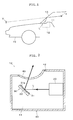
- FIG. 1 to Fig. 4 an embodiment in which the present invention is applied to a head-up display apparatus for a vehicle will be described.
- the head-up display apparatus is an apparatus configured to display a virtual image V by reflecting a display light L which is projected by a display device 12 as a display unit disposed in the interior of an instrument panel 11 of a vehicle 10 toward a driver (user) 14 of the vehicle 10 using a front glass 13 of the vehicle 10, which is a projecting member.
- the head-up display apparatus for a vehicle is configured to illuminate (project) a display light beam L emitted from the display described laser of the display device 12 on the front glass 13 (the projecting member described above), and cause the driver 14 to view a virtual image (displayed image) V obtained by this illumination. Accordingly, the driver 14 can observe the virtual image V displayed forward in front of the driver's seat with a scenery superimposed therewith.
- the display apparatus 12 mainly includes a display 20 as a lighting device, a reflector 30, and a housing 40 as shown in Fig. 2 .
- the display 20 includes a light source unit 23 having plural (two for example) light sources 22 mounted (disposed) on a circuit board 21 as a substrate, a liquid crystal display panel 24 as a lighted member which is transmitted and lighted by the illuminating light beams from the plural light sources 22 therethrough, a diffusing member 25 arranged between the light source unit 23 and the liquid crystal display panel 24, a lens member 26 positioned between the diffusing member 25 and the liquid crystal display panel 24, a case body 27 arranged between the circuit board 21 and the diffusing member 25 (liquid crystal display panel 24) so as to surround the respective light sources 22, and a housing 28 configured to hold and accommodates these members.
- a light source unit 23 having plural (two for example) light sources 22 mounted (disposed) on a circuit board 21 as a substrate
- a liquid crystal display panel 24 as a lighted member which is transmitted and lighted by the illuminating light beams from the plural light sources 22 therethrough
- a diffusing member 25 arranged between the light source unit 23 and the liquid crystal display panel 24
- the circuit board 21 is formed of a hard wiring substrate having a predetermined wiring pattern provided thereon, and includes the respective light sources 22 mounted on the wiring pattern.
- Reference numerals 21a and 21b designate substantially circular-shaped first and second opening holes provided so as to communicate with the first and second screw holes, described later, provided on the case body 27, and the opening holes 21a, 21b are provided on both end sides of the circuit board 21, respectively (see Fig. 4 ).
- the light sources 22 are formed of chip-type light-emitting diodes (LEDs) which emit color as needed, for example, and are light-emitting members which supply illuminating light beams to the diffusing member 25 (the liquid crystal display panel 24).
- LEDs chip-type light-emitting diodes
- the liquid crystal display panel 24 is formed of a TFT (thin-film transistor) type liquid crystal display element having polarizing films provided on the front and back surfaces of a liquid crystal cell formed by encapsulating liquid crystal between a pair of translucent substrates, and is arranged on the front side of the light source unit 23 (the lens member 26) so as to form the display light beam L by allowing the illuminating light beams from the respective light sources 22 (in other words, a parallel outgoing light beam emitted from the lens member 26) to pass therethrough.
- TFT thin-film transistor
- the liquid crystal display panel 24 as described above is capable of displaying a measured value of the speed of the vehicle 10 or the number of revolutions of the engine as a numerical value using an arithmetic circuit (not shown) configured to measure the vehicle speed or the number of revolutions of the engine on the basis of output signals from a vehicle speed sensor or a engine revolution sensor provided on the vehicle 10.
- Displayed information displayed by the liquid crystal display panel 24 is not limited to the vehicle speed or the number of revolutions of the engine, and is arbitrary, and, for example, may be travel distance information, navigation information, or outside temperature information.
- the diffusing member 25 is formed of, for example, a translucent synthetic resin having a milky white color, is formed into a substantially flat-panel shape, is positioned between the case body 27 and the lens member 26 (the liquid crystal display panel 24) and, in this case, is placed on the case body 27 so as to close the upper end side opening of a cavity portion, described later, provided in the case body 27.
- the diffusing member 25 as a placed member described above has a function as a light-diffusing panel for diffusing the illuminating light beams emitted from the respective light sources 22 and proceeding toward the lens member 26 in substantially uniformly.
- the lens member 26 is formed of a translucent synthetic resin, is formed of a convex lens having a flat surface on the back side (the diffusing member 25 side) and a convex surface on the front side (the liquid crystal display panel 24 side), and has a function as a light-collecting member configured to collect diffused outgoing light emitted from the diffusing member 25.
- the lens member 26 is configured cause the diffused outgoing light to be refracted as required, and parallel outgoing light to be converted into a substantially parallel light flux toward the liquid crystal display panel 24.
- the case body 27 is formed of, for example, a synthetic resin, is formed into a substantially frame shape, and includes a cavity portion 50 in which the illuminating light beams from the respective light sources 22 are introduced and a substantially frame shaped body portion 60 provided so as to surround the cavity portion 50.
- the cavity portion 50 is provided so as to correspond to the respective light sources 22, and is formed as a lighting space for guiding the illuminating light beams emitted from the respective light sources 22 toward the diffusing member 25 (that is, toward the liquid crystal display panel 24). Then, in this case, the circuit board 21 is disposed so as to close the lower end side opening 51 of the cavity portion 50, and the diffusing member 25 is placed (disposed) on the case body 27 so as to close the upper end side opening 52 of the cavity portion 50 on the side opposite from the lower end side opening 51.
- the body portion 60 is configured to be divided into two parts in pair as shown in Fig. 4 . More specifically, the body portion 60 is configured to be divided into a first base portion 61 located on the left side in Fig. 4 and a second base portion 62 located on the right side in Fig. 4 . In other words, the body portion 60 is configured to be divided so as to have a pair of the base portions 61, 62 via the cavity portion 50.
- the first base portion 61 and the second base portion 62 have, geometrically speaking, a point symmetry with respect to a center point C of the circuit board 21 that is a virtual center point in Fig. 4 (or a center portion of the diffusing member 25 having substantially the same shape obtained by combining the respective base portions 61 and 62, although detail illustration is omitted) when viewing the case body 27 from the liquid crystal display panel 24 side.
- the first base portion 61 is rotated by 180° about the center point C, the first base portion 61 is overlapped completely with the second base portion 62.
- the first base portion 61 is configured to include a first opposing wall portion 61a formed of an upright wall portion opposing a third opposing wall portion, described later, of the second base portion 62, a second opposed wall portion 61b formed of an upright wall portion opposing a fourth opposing wall portion, described later, of the second base portion 62 and a flat-panel shaped first flange portion 61c extending in the direction of an arrow X in Fig. 4 so as to be in parallel with the circuit board 21 from the lower end side of the first opposing wall portion 61a formed integrally to each other.
- the first opposing wall portion 61a is formed with a first notched portion 61d as a heat releasing portion notched so as to form a depression (recessed) shape for releasing heat generated by the respective light sources 22 to the outside of the case body 27 at a center portion on the upper end side thereof and is formed with a first through hole portion 61e at a boundary portion between the first opposing wall portion 61a and the first flange portion 61c.
- the first through hole portion 61e described above is formed of an opening window portion formed so as to open by hollowing out a substantially center area of the boundary portion between the first opposing wall portion 61a and the first flange portion 61c, and functions as an outside air introducing portion for introducing air (outside air) existing around the case body 27.
- the second opposing wall portion 61b is formed with a second notched portion 61f which is notched so as to form a depression (recessed) shape and functions as a heat releasing portion for releasing heat generated by the respective light sources 22 to the outside of the case body 27 at a center portion on the upper end side thereof
- the second opposed wall portion 61b is formed with a third notched portion 61g which is notched so as to form an inverted depression (recessed) shape and functions as an outside air introducing portion for introducing air (outside air) existing around the case body 27 at a center portion on the lower end side thereof.
- the inner wall portion (inner wall surface) of the first opposing wall portion 61a which corresponds to the boundary portion between the cavity portion 50 and the first base portion 61 and the inner wall portion (inner wall surface) of the second opposed wall portion 61b which corresponds to the boundary portion between the cavity portion 50 and the first base portion 61 are formed with a mirror layer 63 in a mirror state by aluminum depositing, chrome plating, or the like.
- the mirror layer 63 is not formed at a position of the first opposing wall portion 61a opposing the fourth opposing wall portion.
- the first flange portion 61c is formed with a first screw hole 61h provided so as to communicate with the first opening hole 21a provided on the circuit board 21 and allows penetration of a screw portion of a screw S.
- the second base portion 62 includes a third opposing wall portion 62a formed of an upright wall portion opposing the first opposing wall portion 61a, fourth opposed wall portion 62b formed of an upright wall portion opposing a second opposed wall portion 61b, described later, and a flat-panel shaped second flange portion 62c extending in the direction opposite from the arrow X in Fig. 4 so as to be in parallel with the circuit board 21 from the lower end side of the third opposing wall portion 62a formed integrally to each other.
- the third opposed wall portion 62a is formed with a fourth notched portion 62d notched so as to form a depression (recessed) shape and configured to function as a heat releasing portion for releasing heat generated by the respective light sources 22 to the outside of the case body 27 at a center portion on the upper end side of the third opposed wall portion 62a
- the second through hole portion 62e is formed at a boundary portion between the third opposed wall portion 62a and the second flange portion 62c so as to oppose the first through hole portion 61e (see Fig. 3 ).
- the second through hole portion 62e as described above has the substantially same shape as the first through hole portion 61e, is formed of an opening window portion formed so as to open by hollowing out the substantially center area of the boundary portion between the third opposed wall portion 62a and the second flange portion 62c, and functions as an outside air introducing portion for introducing the air (outside air) existing around the case body 27.
- the fourth opposed wall portion 62b is formed with a fifth notched portion 62f notched so as to form a depression (recessed) shape and configured to function as a heat releasing portion for releasing the heat generated by the respective light sources 22 to the outside of the case body 27 at a center portion of the upper end side thereof so as to oppose the second notched portion 61f described above, and the fourth opposed wall portion 62b is formed with a sixth notched portion 62g notched so as to form an inverted depression (recessed) shape for introducing air (outside air) existing around the case body 27 at a center portion of a lower end side thereof so as to oppose the third notched portion 61g.
- the inner wall portion (inner wall surface) of the third opposing wall portion 62a which corresponds to the boundary portion between the cavity portion 50 and the second base portion 62 and the inner wall portion (inner wall surface) of the fourth opposed wall portion 62b which corresponds to the boundary portion between the cavity portion 50 and the second base portion 62 are formed with the above-described mirror layer 63 in a mirror state by aluminum depositing, chrome plating, or the like.
- the mirror layer 63 is not formed at a position of the third opposing wall portion 62a opposing the second opposing wall portion 61b.
- the second flange portion 62c is formed with a second screw hole 62h provided so as to communicate with the second opening hole 21b provided on the circuit board 21 and allows penetration of a screw portion of a screw S.
- the housing 28 is formed of a synthetic resin material and formed into a substantially box shape, and has a function as a storage member configured to store the light source unit 23, the liquid crystal display panel 24, the diffusing member 25, the lens member 26 and the case body 27, and includes an opening portion 28a for causing a display area (not shown) of the liquid crystal display panel 24 to face therein.
- the first base portion 61 and the second base portion 62 are positioned so that the inner wall portion of the first opposing wall portion 61a and the inner wall portion of the third opposed wall portion 62a oppose each other, and the inner wall portion of the second opposed wall portion 61b and the inner wall portion of the fourth opposed wall portion 62b oppose each other, respectively.
- a double-face tape (not shown) is adhered on a first side surface portion R1 which is a portion of the second opposed wall portion 61b corresponding to the third opposed wall portion 62a and a second side surface portion R2 which is a portion of the fourth opposed wall portion 62b corresponding to the first opposing wall portion 61a.
- the first side surface portion R1 is joined to the portion of the third opposed wall portion 62a opposing thereto and, simultaneously, the second side surface portion R2 is joined to the portion of the first opposing wall portion 61a opposing thereto.
- the cavity portion 50 which is the lighting space is formed in a space area surrounded by the first base portion 61 and the second base portion 62, and the periphery of the cavity portion 50 provided so as to correspond to the respective light sources 22 are surrounded by the mirror layer 63.
- the case body 27 is placed on the circuit board 21 so that the first screw hole 61h of the first flange portion 61c communicates with the first opening hole 21a of the circuit board 21 and the second screw hole 62h of the second flange portion 62c communicates with the second opening hole 21b of the circuit board 21.
- the screw portions of the screws S are passed through the first and second screw holes 61h, 62h and the first and second opening holes 21a, 21b from the front side of the first and second flange portions 61c, 62c, and nuts N are screwed into lower end portions of the screw portions that protrudes toward the back side of the circuit board 21, whereby the circuit board 21 and the case body 27 are overlapped into tight contact with each other and the assembly of the circuit board 21 and the case body 27 is completed.
- a first gap portion, not illustrated, formed of a substantially rectangular shaped opening window is formed between the circuit board 21 and the second opposed wall portion 61b and, in the same manner, since the sixth notched portion 62g is provided at a lower end portion of the fourth opposed wall portion 62b, a second gap portion, not shown, formed of a substantially rectangular shaped opening window is formed between the circuit board 21 and the fourth opposed wall portion 62b.
- the diffusing member 25 is mounted on the case body 27 (the body portion 60) using a mounting means as needed. At this time, the diffusing member 25 is supported by a surface portion of the first base portion 61 except for the first and second notched portions 61d, 61f and a surface portion of the second base portion 62 except for the fourth, fifth notched portions 62d, 62f.
- a third gap portion 71 (see Fig. 3 ) formed of a substantially rectangular shaped opening window is formed between the diffusing member 25 and the first opposing wall portion 61a and, since the second notched portion 61f formed into the recessed shape is provided at the upper end portion of the second opposed wall portion 61b, a fourth gap portion, not shown, formed into a substantially rectangular shaped opening window is formed between the diffusing member 25 and the second opposed wall portion 61b.
- a fifth gap portion 72 (see Fig. 3 ) formed of a substantially rectangular shaped opening window is formed between the diffusing member 25 and the third opposed wall portion 62a and the fifth notched portion 62f formed into the recessed shape is provided at the upper end portion of the fourth opposed wall portion 62b, a sixth gap portion, not shown, formed of a substantially rectangular shaped opening window is formed between the diffusing member 25 and the fourth opposed wall portion 62b.
- the illuminating light beams emitted from the respective light sources 22 pass from the lower end side opening 51 of the cavity portion 50 which is the peripheries of the respective light sources 22 through the upper end side opening 52 of the cavity portion 50, and is guided to the diffusing member 25 placed on the case body 27.
- the heat emitted from the respective light sources 22 stays in the vicinity of the lower end side opening 51 which is the peripheries of the light sources 22, then, caused by expansion of air in the vicinity of the lower end side opening 51 where the heat stays, the specific gravity of the air is lowered and hence the heat (the air) moves from the lower end side opening 51 toward the upper end side opening 52, then the heat moved toward the upper end side opening 52 is released to the outside of the case body 27 from the notched portions 61d, 61f, 62d, 62f (that is, the third and fifth gap portions 71, 72 and the fourth and sixth gap portions) as the heat releasing portions formed on the body portion 60 (the case body 27) so as to communicate with the upper end side opening 52 (the cavity portion 50).
- the cavity portion 50 is brought into a negative pressure, and the outside air is introduced into the lower end side opening 51 of the cavity portion 50 via the first and second through hole portions 61e, 62e and the third and sixth notched portions 61g, 62g as the outside air introducing portions.
- the cavity portion 50 is inhibited from going to a high-temperature state in association with an air circulation in the cavity portion 50 generating in such a manner that the heated air is released from the cavity portion 50 to the outside of the case body 27 through the notched portions 61d, 61f, 62d, 62f as the heat releasing portions, and the outside air is introduced from the outside of the case body 27 into the cavity portion 50 via the first and second through hole portions 61e, 62e and the third and sixth notched portions 61g, 62g as the outside air introducing portion.
- the heat generated in association with the light emission of the respective light sources 22 can hardly be transmitted to the case body 27 or the diffusing member 25 positioned in the periphery of the cavity portion 50, deformation of the case body 27 or the diffusing member 25 can be prevented as much as possible.
- the illuminating light beams emitted from the respective light sources 22 are supplied efficiently toward the liquid crystal display panel 24 in a state in which lighting variations or the like are inhibited, the probability of lowering of the illumination quality of the liquid crystal display panel 24 is eliminated.
- the illuminating light beams emitted from the respective light sources 22 partly leak to the outside of the case body 27 from the first and second through hole portions 61e, 62e, the third and fifth gap portions 71, 72, the first, second, fourth, and sixth gap portions, since the mirror layer 63 is formed on the inner wall portions of the respective base portions 61, 62, the light beams are guided to the diffusing member 25 while being secured in light amount to some extent.
- the diffused outgoing light going out from the diffusing member 25 passes through the lens member 26, and goes out from the lens member 26 as the parallel outgoing light.
- the liquid crystal display panel 24 is lighted by the parallel outgoing light going out from the lens member 26 therethrough, whereby the display light beam L is emitted from the liquid crystal display panel 24.
- the display light beam L emitted from the liquid crystal display panel 24 passes through the opening portion 28a of the housing 28 and guided toward the reflector 30.
- the reflector 30 includes a concave mirror (reflecting member) 31 configured to reflect the display light beam L emitted from the liquid crystal display panel 24, and a mirror holder (holding member) 32 formed of a synthetic resin configured to hold the concave mirror 31.
- the concave mirror 31 is formed by depositing a reflecting layer 31a on the resin substrate formed of polycarbonate having a depressed surface.
- the concave mirror 31 in this configuration is disposed in an inclined state at a position where the reflecting layer 31a thereof opposes the liquid crystal display panel 24 and the translucent cover, described later, of the housing 40 and can be approached from the translucent cover.
- the concave mirror 31 is configured to reflect the display light L from display 20 toward the side of the translucent cover (the front glass 13 of the vehicle 10) while enlarging the scale thereof. This means that the concave mirror 31 enlarges the display light L emitted from the display 20 and projects the enlarged display light L to the front glass 13 via the translucent cover.
- the concave mirror 31 is adhered to the mirror holder 32 with a double-face adhesive tape.
- the housing 40 is formed of a black light-shielding synthetic resin material, is formed into a substantially box shape, is configured to hold and accommodate the display 20 and the reflector 30 in the space portion 41 as the internal space thereof, and includes an opening window 42 opening on an upper portion (the front glass 13 side) of the concave mirror 31 of the reflector 30.
- a translucent cover 43 as a light-output portion so as to close the opening window 42.
- the translucent cover 43 as described above is formed of translucent synthetic resin material (for example, acrylic resin), and has a function as the light-translucent member which allows transmission (passage) of the display light L reflected by the concave mirror 31.
- the display light beam L reflected by the concave mirror 31 is projected on the front glass 13 through the translucent cover 43 formed on the housing 40, whereby the driver 14 views the virtual image V obtained by this projection.
- the case body 27 arranged between the circuit board 21 and the liquid crystal display panel 24 and includes the cavity portion 50 provided so as to correspond to the respective light sources 22, and the diffusing member 25 as a placed member positioned between the case body 27 and the liquid crystal display panel 24 and is placed on the case body 27, wherein the circuit board 21 is disposed so as to close the lower end side opening 51 of the cavity portion 50 and the diffusing member 25 is disposed so as to close the upper end side opening 52 of the cavity portion 50 on the side opposite from the lower end side opening 51, the case body 27 is formed with heat releasing portions 61d, 61f, 62d, 62f for releasing heat generated by the respective light sources 22 to the outside of the case body 27.
- the heat emitted from the respective light sources 22 is released to the outside of the case body 27 from the cavity portion 50 through the first, second, fourth and fifth notched portions 61d, 61f, 62d, 62f (that is, the third and fifth gap portions 71, 72 and the fourth and sixth gap portions) as heat releasing portions provided so as to communicate with the upper end side opening 52 as described above, the deformation of the case body 27 or the diffusing member 25 due to the heat generated when the respective light sources 22 emit light beams.
- the illuminating light beams emitted from the respective light sources 22 are supplied efficiently toward the liquid crystal display panel 24 in a state in which lighting variations or the like are inhibited, the probability of lowering of the illumination quality of the liquid crystal display panel 24 is eliminated.
- the cavity portion 50 as the lighting space is formed by the circuit board 21, the diffusing member 25, and the case body 27 (the body portion 60)
- the diffusing member 25 and the lens member 26 are eliminated and the liquid crystal display panel 24 is placed on the case body 27, and the cavity portion 50 as the lighting space is formed by the circuit board 21, the liquid crystal display panel 24, and the case body 27 (the body portion 60) is also applicable.
- the liquid crystal display panel 24 is configured to be placed (disposed) on the case body 27 so as to close the upper end side opening 52 of the cavity portion 50 on the side opposite from the lower end side opening 51.
- first and second through hole portions 61e, 62e and the third and sixth notched portions 61g, 62g are eliminated and four through holes penetrating through the panel thickness of the respective opposing wall portions 61a, 61b, 62a, 62b are provided on predetermined positions of the respective opposing wall portions 61a, 61b, 62a, 62b (for example, at the substantially center area or a lower side with respect to the substantially center area), and the outside air is taken from the outside of the case body 27 into the cavity portion 50 using these through holes is also applicable.
- the number of through hole portions and notched portions for introducing outside air is arbitrary, and through hole portions and notched portions for introducing outside air and the through holes may be mixed.
- first through hole portion 61e is provided at the boundary portion between the first opposing wall portion 61a and the first flange portion 61c of the first base portion 61
- second through hole portion 62e is provided at the boundary portion between the third opposed wall portion 62a and the second flange portion 62c of the second base portion 62
- first hole portion 21c formed of a substantially rectangular-shaped through hole communicating with the first through hole portion 61e
- second hole portion 21d formed of a substantially rectangular-shaped through hole communicating with the the second through hole portion 62e are provided on the circuit board 21 as shown in Fig.
- the surface portion P of the circuit board 21 is provided with the wiring pattern 80 for supplying lighting power to the two light sources 22, and the wiring pattern 80 includes a first wiring portion 81, a second wiring portion 82, and a third wiring portion 83.
- the first wiring portion 81 is formed of a linear electrically conducting path for conductively connecting a first terminal portion (not shown) of the first connector 84 mounted on the circuit board 21 and one of a pair of power feeding terminals, not shown, (the power feeding terminal positioned on the lower side of the first light source 22a in Fig. 6 ) provided on the light source 22 located on the left side in Fig. 6 (hereinafter, referred to as first light source 22a).
- the second wiring portion 82 is formed of a substantially angular U-shaped electrically-conducting path for conductively connecting the other power feeding terminal (not shown) of the first light source 22a located on the side opposite from the one power feeding terminal of the first light source 22a and one of the pair of power feeding terminals, not shown, (the power feeding terminal positioned on the upper side of the second light source 22b in Fig. 6 ) provided on the power source 22 located on the right side in Fig. 6 (hereinafter, referred to as the second light source 22b).
- the third wiring portion 83 is formed of a linear electrically-conducting path for conductively connecting the other power feeding terminal (not shown) of the second light source 22b located on the side opposite from the one power feeding terminal of the second light source 22b and the lower side of the second light source 22b and the second terminal portion (not shown) of the first connector 84.
- the second connector provided on a main substrate having a micro computer configured to control the drive circuit configured to drive the liquid crystal, a light source drive circuit configured to drive the respective light sources 22a, 22b, control means including a microcomputer configured to control the drive circuit and the light source drive circuit mounted in a predetermined circuit pattern and the first connector 84 are electrically connected via a wiring member such as an electric cord or the like.
- the second connector is mounted on the circuit pattern, as a matter of course.
- the light source drive circuit is conductively connected to the first and second light sources 22a, 22b via the circuit pattern, the second connector, the wiring member, the first connector 84, and the wiring pattern 80. Then, when the control means issues a command signal for lighting the respective light sources 22a, 22b to the light source drive circuit, the light source drive circuit receives the command signal, and lights the respective light sources 22a, 22b. In other words, at this time, a lighting power is supplied from the light source drive circuit to the respective light sources 22a, 22b via the circuit pattern, the second connector, the wiring member, the first connector 84 and the wiring pattern 80, so that the respective light sources 22a, 22b light (emit light beams).
- the wiring pattern 80 is provided so as to circumvent the portion where the circuit board 21 and the case body 27 are in abutment.
- the first and third wiring portions 81, 83 of the wiring pattern 80 are provided respectively at a surface portion of the circuit board 21 corresponding to the cavity portion 50 as the lighting space (the inner space of the body portion 60), a surface portion of the circuit board 21 corresponding to the sixth notched portion 62g formed on the lower end side of the case body 27 (the fourth opposed wall portion 62b), and a surface portion of the circuit board 21 between the outer wall surface of the fourth opposed wall portion 62b and the first connector 84, the circuit board 21 and the case body 27, and hence do not exist at all at the portion where the circuit board 21 and the case body 27 are in abutment as a consequence.
- the second wiring portion 82 of the wiring pattern 80 is provided on the surface portion of the circuit board 21 corresponding to the cavity portion 50, and hence does not exist at all at the portion where the circuit board 21 and the case body 27 are in abutment as a consequence.
- the case body 27 is placed on the circuit board 21 so as to incline slightly instead of upright position, which may affect adversely to the lighting efficiency of the illuminating light beams from the respective light sources 22a, 22b to the diffusing member 25.
- the wiring pattern 80 is provided on the surface of the circuit board 21 so as to circumvent the position where the circuit board 21 and the case body 27 come into abutment, the lower end surfaces of the four opposing wall portions 61a, 61b, 62a, 62b which are flat shape and the surface portion (flat portion) of the circuit board 21 come into contact with each other, so that the case body 27 can be placed (fixed) onto the circuit board 21 so that the case body 27 is positioned in an upright posture.
- the shapes of the respective wiring portions 81, 82, 83 of the wiring pattern 80 can be set freely as long as the shape where the circuit board 21 and the case body 27 come into abutment is circumvented.
- the number of light sources 22 mounted on the circuit board 21 may be one, or three or more.
- a combiner film for reflecting the display light beam L desirably toward the driver 14 may be provided on the front glass 13, or the display light beam L may be projected on a specific reflecting body separate from the front glass 13.
- the present invention is applicable to a lighting device including a light source unit having the light source mounted on a substrate and a illuminated member such as a liquid crystal panel or the like transmitted and lighted by the illuminating light beams from the light source therethrough.
Landscapes
- Physics & Mathematics (AREA)
- General Physics & Mathematics (AREA)
- Optics & Photonics (AREA)
- Engineering & Computer Science (AREA)
- General Engineering & Computer Science (AREA)
- Liquid Crystal (AREA)
- Electromagnetism (AREA)
- Planar Illumination Modules (AREA)
- Arrangement Of Elements, Cooling, Sealing, Or The Like Of Lighting Devices (AREA)
- Illuminated Signs And Luminous Advertising (AREA)
Abstract
Description
- The present invention relates to a lighting device configured to light a liquid crystal display panel (lighted member) mounted on a head up display, for example.
- In the related art, as a lighting device of this type, for example, the one described in
Patent Document 1 shown below is known. The lighting device described inPatent Document 1 includes a light source unit having a light source (LED) mounted (disposed) on a substrate as a circuit board, a liquid crystal display panel (lighted member) to be lighted by an illuminating light beam from the light source, a case member arranged between the substrate and the liquid crystal display panel and formed of a synthetic resin having a cavity portion provided so as to correspond to the light source, and a diffusing member interposed between the case member and the liquid crystal display panel and placed on the case body. - Then, in this case, the case body are placed on the substrate so as to surround the light source, and the diffusing member and the liquid crystal display panel is arranged on the case body in a stacked manner so that the liquid crystal display panel is positioned at an uppermost position. In other words, it means that the substrate of the light source unit is disposed so as to close an opening on a lower end side of the cavity portion and the diffusing member (the liquid crystal display panel) is disposed so as to close an opening on an upper end side of the cavity portion on the opposite side from the opening on the lower end side.
- In this configuration, the illuminating light beam emitted from the light source passes the cavity portion, which corresponds to the inner portion of the case member, is substantially uniformized through the diffusing member placed on the case body, and the uniformized illumination light beam lights through the liquid crystal display panel placed on the diffusing member. Accordingly, the liquid crystal display panel is lighted by a back light.
-
- Patent Document 1:
JP-A-2005-181640 - In the case of the lighting device described in
Patent Document 1, the case body is arranged between the diffusing member (liquid crystal display panel) and the substrate, and the cavity portion surrounded by the diffusing member, the substrate, and the case body is formed as a sealed space, and hence there arises a problem in that heat generated when the light source emits a light beam stays in the sealed space. When the heat stays in the closed space, the case body or the like positioned in the periphery of the sealed space may be deformed by going into a high-temperature state , and hence the lowering of the lighting quality of the liquid crystal display panel which is a lighted member may be resulted.
In order to cope with the problem as described above, it is an object of the present invention to provide a lighting device which prevents a case body or the like from deforming due to heat generated when a light source emits a light beam and eliminates a provability of lowering of the lighting quality of a lighted member. - A lighting device according to the present invention is a lighting device including: a light source unit having a light source disposed on a substrate; a lighted member arranged on the front side of the light source unit and lighted by an illuminating light beam from the light source; and a case member arranged between the substrate and the lighted member and includes a cavity portion provided so as to correspond to the light source, wherein the substrate is disposed so as to close an opening on a lower end side of the cavity portion and the lighted member is disposed so as to close an opening on an upper end side of the cavity portion on the side opposite from the lower end side opening, and the case member is formed with a heat releasing portion for releasing heat generated by the light source to the outside of the case body.
- The present invention is a lighting device including: a light source unit having a light source disposed on a substrate; a lighted member arranged on the front side of the light source unit and lighted by an illuminating light beam from the light source; a case member arranged between the substrate and the lighted member and includes a cavity portion provided so as to correspond to the light source; and a placed member positioned between the case member and the light member and placed on the case body, wherein the substrate is disposed so as to close an opening on a lower end side of the cavity portion and the placed member is disposed so as to close an opening on an upper end side of the cavity portion on the side opposite from the lower end side opening and the case member is formed with a heat releasing portion for releasing heat generated by the light source to the outside of the case body.
- The present invention is also characterized in that the heat releasing portion is formed of a notched portion or a through hole portion formed on the case body so as to communicate with the cavity portion.
- The present invention is also characterized in that the substrate is provide with a wiring pattern configured to supply lighting power to the light source, and the wiring pattern is provided on the substrate so as to circumvent a portion where the substrate and the case member come into abutment.
- According to the present invention, the initial object can be achieved, and there is provided a lighting device which prevents a case body or the like from deforming due to heat generated when a light source emits a light beam and eliminates provability of lowering of the lighting quality of a lighted member is provided.
-
- [
Fig. 1] Fig. 1 is a schematic view of a head-up display apparatus according to an embodiment of the present invention. - [
Fig. 2] Fig. 2 is a cross-sectional view of the display device according to the same embodiment. - [
Fig. 3 ]Fig. 2 is a cross-sectional view of the lighting device according to the same embodiment. - [
Fig. 4] Fig. 4 is a perspective view showing a case body and a substrate according to the same embodiment. - [
Fig. 5] Fig. 5 is a perspective view showing a case body and a substrate according to a modification of the same embodiment. - [
Fig. 6 ]Fig. 5 is a perspective view showing a case body and a substrate according to another modification of the same embodiment. - Referring now to
Fig. 1 to Fig. 4 , an embodiment in which the present invention is applied to a head-up display apparatus for a vehicle will be described. - The head-up display apparatus is an apparatus configured to display a virtual image V by reflecting a display light L which is projected by a
display device 12 as a display unit disposed in the interior of aninstrument panel 11 of avehicle 10 toward a driver (user) 14 of thevehicle 10 using afront glass 13 of thevehicle 10, which is a projecting member. In other words, the head-up display apparatus for a vehicle is configured to illuminate (project) a display light beam L emitted from the display described laser of thedisplay device 12 on the front glass 13 (the projecting member described above), and cause thedriver 14 to view a virtual image (displayed image) V obtained by this illumination. Accordingly, thedriver 14 can observe the virtual image V displayed forward in front of the driver's seat with a scenery superimposed therewith. - The
display apparatus 12 mainly includes adisplay 20 as a lighting device, areflector 30, and ahousing 40 as shown inFig. 2 . - As shown in
Fig. 3 in detail, thedisplay 20 includes alight source unit 23 having plural (two for example)light sources 22 mounted (disposed) on acircuit board 21 as a substrate, a liquidcrystal display panel 24 as a lighted member which is transmitted and lighted by the illuminating light beams from theplural light sources 22 therethrough, a diffusingmember 25 arranged between thelight source unit 23 and the liquidcrystal display panel 24, alens member 26 positioned between the diffusingmember 25 and the liquidcrystal display panel 24, acase body 27 arranged between thecircuit board 21 and the diffusing member 25 (liquid crystal display panel 24) so as to surround therespective light sources 22, and ahousing 28 configured to hold and accommodates these members. - The
circuit board 21 is formed of a hard wiring substrate having a predetermined wiring pattern provided thereon, and includes therespective light sources 22 mounted on the wiring pattern.Reference numerals case body 27, and theopening holes circuit board 21, respectively (seeFig. 4 ). - The
light sources 22 are formed of chip-type light-emitting diodes (LEDs) which emit color as needed, for example, and are light-emitting members which supply illuminating light beams to the diffusing member 25 (the liquid crystal display panel 24). - The liquid
crystal display panel 24 is formed of a TFT (thin-film transistor) type liquid crystal display element having polarizing films provided on the front and back surfaces of a liquid crystal cell formed by encapsulating liquid crystal between a pair of translucent substrates, and is arranged on the front side of the light source unit 23 (the lens member 26) so as to form the display light beam L by allowing the illuminating light beams from the respective light sources 22 (in other words, a parallel outgoing light beam emitted from the lens member 26) to pass therethrough. - The liquid
crystal display panel 24 as described above is capable of displaying a measured value of the speed of thevehicle 10 or the number of revolutions of the engine as a numerical value using an arithmetic circuit (not shown) configured to measure the vehicle speed or the number of revolutions of the engine on the basis of output signals from a vehicle speed sensor or a engine revolution sensor provided on thevehicle 10. - Displayed information displayed by the liquid
crystal display panel 24 is not limited to the vehicle speed or the number of revolutions of the engine, and is arbitrary, and, for example, may be travel distance information, navigation information, or outside temperature information. - The diffusing
member 25 is formed of, for example, a translucent synthetic resin having a milky white color, is formed into a substantially flat-panel shape, is positioned between thecase body 27 and the lens member 26 (the liquid crystal display panel 24) and, in this case, is placed on thecase body 27 so as to close the upper end side opening of a cavity portion, described later, provided in thecase body 27. The diffusingmember 25 as a placed member described above has a function as a light-diffusing panel for diffusing the illuminating light beams emitted from therespective light sources 22 and proceeding toward thelens member 26 in substantially uniformly. - The
lens member 26 is formed of a translucent synthetic resin, is formed of a convex lens having a flat surface on the back side (the diffusingmember 25 side) and a convex surface on the front side (the liquidcrystal display panel 24 side), and has a function as a light-collecting member configured to collect diffused outgoing light emitted from the diffusingmember 25. In other words, thelens member 26 is configured cause the diffused outgoing light to be refracted as required, and parallel outgoing light to be converted into a substantially parallel light flux toward the liquidcrystal display panel 24. - The
case body 27 is formed of, for example, a synthetic resin, is formed into a substantially frame shape, and includes acavity portion 50 in which the illuminating light beams from therespective light sources 22 are introduced and a substantially frame shapedbody portion 60 provided so as to surround thecavity portion 50. - The
cavity portion 50 is provided so as to correspond to therespective light sources 22, and is formed as a lighting space for guiding the illuminating light beams emitted from therespective light sources 22 toward the diffusing member 25 (that is, toward the liquid crystal display panel 24). Then, in this case, thecircuit board 21 is disposed so as to close the lower end side opening 51 of thecavity portion 50, and the diffusingmember 25 is placed (disposed) on thecase body 27 so as to close the upper end side opening 52 of thecavity portion 50 on the side opposite from the lower end side opening 51. - The
body portion 60 is configured to be divided into two parts in pair as shown inFig. 4 . More specifically, thebody portion 60 is configured to be divided into afirst base portion 61 located on the left side inFig. 4 and asecond base portion 62 located on the right side inFig. 4 . In other words, thebody portion 60 is configured to be divided so as to have a pair of thebase portions cavity portion 50. - Also, in this case, the
first base portion 61 and thesecond base portion 62 have, geometrically speaking, a point symmetry with respect to a center point C of thecircuit board 21 that is a virtual center point inFig. 4 (or a center portion of the diffusingmember 25 having substantially the same shape obtained by combining therespective base portions case body 27 from the liquidcrystal display panel 24 side. In other words, when thefirst base portion 61 is rotated by 180° about the center point C, thefirst base portion 61 is overlapped completely with thesecond base portion 62. - The
first base portion 61 is configured to include a firstopposing wall portion 61a formed of an upright wall portion opposing a third opposing wall portion, described later, of thesecond base portion 62, a second opposedwall portion 61b formed of an upright wall portion opposing a fourth opposing wall portion, described later, of thesecond base portion 62 and a flat-panel shapedfirst flange portion 61c extending in the direction of an arrow X inFig. 4 so as to be in parallel with thecircuit board 21 from the lower end side of the firstopposing wall portion 61a formed integrally to each other. - In
Fig. 4 , the firstopposing wall portion 61a is formed with a first notchedportion 61d as a heat releasing portion notched so as to form a depression (recessed) shape for releasing heat generated by therespective light sources 22 to the outside of thecase body 27 at a center portion on the upper end side thereof and is formed with a first throughhole portion 61e at a boundary portion between the firstopposing wall portion 61a and thefirst flange portion 61c. - The first through
hole portion 61e described above is formed of an opening window portion formed so as to open by hollowing out a substantially center area of the boundary portion between the firstopposing wall portion 61a and thefirst flange portion 61c, and functions as an outside air introducing portion for introducing air (outside air) existing around thecase body 27. - Furthermore, in
Fig. 4 , the secondopposing wall portion 61b is formed with a second notchedportion 61f which is notched so as to form a depression (recessed) shape and functions as a heat releasing portion for releasing heat generated by therespective light sources 22 to the outside of thecase body 27 at a center portion on the upper end side thereof, and the secondopposed wall portion 61b is formed with a third notchedportion 61g which is notched so as to form an inverted depression (recessed) shape and functions as an outside air introducing portion for introducing air (outside air) existing around thecase body 27 at a center portion on the lower end side thereof. - Also, the inner wall portion (inner wall surface) of the first
opposing wall portion 61a which corresponds to the boundary portion between thecavity portion 50 and thefirst base portion 61 and the inner wall portion (inner wall surface) of the secondopposed wall portion 61b which corresponds to the boundary portion between thecavity portion 50 and thefirst base portion 61 are formed with amirror layer 63 in a mirror state by aluminum depositing, chrome plating, or the like. - Although detailed illustration is omitted, in
Fig. 4 , themirror layer 63 is not formed at a position of the firstopposing wall portion 61a opposing the fourth opposing wall portion. Thefirst flange portion 61c is formed with afirst screw hole 61h provided so as to communicate with thefirst opening hole 21a provided on thecircuit board 21 and allows penetration of a screw portion of a screw S. - In the same manner, the
second base portion 62 includes a thirdopposing wall portion 62a formed of an upright wall portion opposing the firstopposing wall portion 61a, fourthopposed wall portion 62b formed of an upright wall portion opposing a secondopposed wall portion 61b, described later, and a flat-panel shapedsecond flange portion 62c extending in the direction opposite from the arrow X inFig. 4 so as to be in parallel with thecircuit board 21 from the lower end side of the thirdopposing wall portion 62a formed integrally to each other. - Then, in
Fig. 4 , the thirdopposed wall portion 62a is formed with a fourth notchedportion 62d notched so as to form a depression (recessed) shape and configured to function as a heat releasing portion for releasing heat generated by therespective light sources 22 to the outside of thecase body 27 at a center portion on the upper end side of the third opposedwall portion 62a, and the second throughhole portion 62e is formed at a boundary portion between the third opposedwall portion 62a and thesecond flange portion 62c so as to oppose the first throughhole portion 61e (seeFig. 3 ). - Although detailed illustration is omitted, the second through
hole portion 62e as described above has the substantially same shape as the first throughhole portion 61e, is formed of an opening window portion formed so as to open by hollowing out the substantially center area of the boundary portion between the third opposedwall portion 62a and thesecond flange portion 62c, and functions as an outside air introducing portion for introducing the air (outside air) existing around thecase body 27. - Furthermore, in
Fig. 4 , the fourthopposed wall portion 62b is formed with a fifth notchedportion 62f notched so as to form a depression (recessed) shape and configured to function as a heat releasing portion for releasing the heat generated by therespective light sources 22 to the outside of thecase body 27 at a center portion of the upper end side thereof so as to oppose the second notchedportion 61f described above, and the fourthopposed wall portion 62b is formed with a sixth notchedportion 62g notched so as to form an inverted depression (recessed) shape for introducing air (outside air) existing around thecase body 27 at a center portion of a lower end side thereof so as to oppose the third notchedportion 61g. - Also, the inner wall portion (inner wall surface) of the third opposing
wall portion 62a which corresponds to the boundary portion between thecavity portion 50 and thesecond base portion 62 and the inner wall portion (inner wall surface) of the fourthopposed wall portion 62b which corresponds to the boundary portion between thecavity portion 50 and thesecond base portion 62 are formed with the above-describedmirror layer 63 in a mirror state by aluminum depositing, chrome plating, or the like. - Although detailed illustration is omitted, in
Fig. 4 , themirror layer 63 is not formed at a position of the third opposingwall portion 62a opposing the second opposingwall portion 61b. Also, thesecond flange portion 62c is formed with asecond screw hole 62h provided so as to communicate with thesecond opening hole 21b provided on thecircuit board 21 and allows penetration of a screw portion of a screw S. - The
housing 28 is formed of a synthetic resin material and formed into a substantially box shape, and has a function as a storage member configured to store thelight source unit 23, the liquidcrystal display panel 24, the diffusingmember 25, thelens member 26 and thecase body 27, and includes anopening portion 28a for causing a display area (not shown) of the liquidcrystal display panel 24 to face therein. - Subsequently, focusing on the
circuit board 21 and thecase body 27, an assembly example for assembling both members will be described. First of all, thefirst base portion 61 and thesecond base portion 62 are positioned so that the inner wall portion of the first opposingwall portion 61a and the inner wall portion of the thirdopposed wall portion 62a oppose each other, and the inner wall portion of the secondopposed wall portion 61b and the inner wall portion of the fourthopposed wall portion 62b oppose each other, respectively. - Subsequently, a double-face tape (not shown) is adhered on a first side surface portion R1 which is a portion of the second
opposed wall portion 61b corresponding to the thirdopposed wall portion 62a and a second side surface portion R2 which is a portion of the fourthopposed wall portion 62b corresponding to the first opposingwall portion 61a. - Then, by moving the
second base portion 62 in parallel along the arrow X direction from this state, the first side surface portion R1 is joined to the portion of the thirdopposed wall portion 62a opposing thereto and, simultaneously, the second side surface portion R2 is joined to the portion of the first opposingwall portion 61a opposing thereto. Then, thecavity portion 50, which is the lighting space is formed in a space area surrounded by thefirst base portion 61 and thesecond base portion 62, and the periphery of thecavity portion 50 provided so as to correspond to the respectivelight sources 22 are surrounded by themirror layer 63. - Subsequently, the
case body 27 is placed on thecircuit board 21 so that thefirst screw hole 61h of thefirst flange portion 61c communicates with thefirst opening hole 21a of thecircuit board 21 and thesecond screw hole 62h of thesecond flange portion 62c communicates with thesecond opening hole 21b of thecircuit board 21. - Finally, the screw portions of the screws S are passed through the first and
second screw holes second opening holes second flange portions circuit board 21, whereby thecircuit board 21 and thecase body 27 are overlapped into tight contact with each other and the assembly of thecircuit board 21 and thecase body 27 is completed. - At this time, since the third notched
portion 61g formed into the recessed shape is provided at the lower end portion of the secondopposed wall portion 61b, a first gap portion, not illustrated, formed of a substantially rectangular shaped opening window is formed between thecircuit board 21 and the secondopposed wall portion 61b and, in the same manner, since the sixth notchedportion 62g is provided at a lower end portion of the fourthopposed wall portion 62b, a second gap portion, not shown, formed of a substantially rectangular shaped opening window is formed between thecircuit board 21 and the fourthopposed wall portion 62b. - After the completion of the assembly of the
circuit board 21 and thecase body 27, the diffusingmember 25 is mounted on the case body 27 (the body portion 60) using a mounting means as needed. At this time, the diffusingmember 25 is supported by a surface portion of thefirst base portion 61 except for the first and second notchedportions second base portion 62 except for the fourth, fifth notchedportions - At this time, since the first notched
portion 61d formed into the recessed shape is provided at the upper end portion of the first opposingwall portion 61a, a third gap portion 71 (seeFig. 3 ) formed of a substantially rectangular shaped opening window is formed between the diffusingmember 25 and the first opposingwall portion 61a and, since the second notchedportion 61f formed into the recessed shape is provided at the upper end portion of the secondopposed wall portion 61b, a fourth gap portion, not shown, formed into a substantially rectangular shaped opening window is formed between the diffusingmember 25 and the secondopposed wall portion 61b. - Also, since the fourth notched
portion 62d formed into the recessed shape is provided at the upper end portion of the thirdopposed wall portion 62a, a fifth gap portion 72 (seeFig. 3 ) formed of a substantially rectangular shaped opening window is formed between the diffusingmember 25 and the thirdopposed wall portion 62a and the fifth notchedportion 62f formed into the recessed shape is provided at the upper end portion of the fourthopposed wall portion 62b, a sixth gap portion, not shown, formed of a substantially rectangular shaped opening window is formed between the diffusingmember 25 and the fourthopposed wall portion 62b. - In this configuration, the illuminating light beams emitted from the respective
light sources 22 pass from the lower end side opening 51 of thecavity portion 50 which is the peripheries of the respectivelight sources 22 through the upper end side opening 52 of thecavity portion 50, and is guided to the diffusingmember 25 placed on thecase body 27. - At this time, the heat emitted from the respective
light sources 22 stays in the vicinity of the lower end side opening 51 which is the peripheries of thelight sources 22, then, caused by expansion of air in the vicinity of the lower end side opening 51 where the heat stays, the specific gravity of the air is lowered and hence the heat (the air) moves from the lower end side opening 51 toward the upperend side opening 52, then the heat moved toward the upperend side opening 52 is released to the outside of thecase body 27 from the notchedportions fifth gap portions - Then, when the heat moved toward the upper end side opening 52 in this manner is released to the outside of the
case body 27 in this manner, thecavity portion 50 is brought into a negative pressure, and the outside air is introduced into the lower end side opening 51 of thecavity portion 50 via the first and second throughhole portions portions - In other words, in the case of this embodiment, the
cavity portion 50 is inhibited from going to a high-temperature state in association with an air circulation in thecavity portion 50 generating in such a manner that the heated air is released from thecavity portion 50 to the outside of thecase body 27 through the notchedportions case body 27 into thecavity portion 50 via the first and second throughhole portions portions - Therefore, since the heat generated in association with the light emission of the respective
light sources 22 can hardly be transmitted to thecase body 27 or the diffusingmember 25 positioned in the periphery of thecavity portion 50, deformation of thecase body 27 or the diffusingmember 25 can be prevented as much as possible. In this manner, by preventing the deformation of thecase body 27 or the diffusingmember 25, the illuminating light beams emitted from the respectivelight sources 22 are supplied efficiently toward the liquidcrystal display panel 24 in a state in which lighting variations or the like are inhibited, the probability of lowering of the illumination quality of the liquidcrystal display panel 24 is eliminated. - Although the illuminating light beams emitted from the respective
light sources 22 partly leak to the outside of thecase body 27 from the first and second throughhole portions fifth gap portions mirror layer 63 is formed on the inner wall portions of therespective base portions member 25 while being secured in light amount to some extent. - Then, the diffused outgoing light going out from the diffusing
member 25 passes through thelens member 26, and goes out from thelens member 26 as the parallel outgoing light. The liquidcrystal display panel 24 is lighted by the parallel outgoing light going out from thelens member 26 therethrough, whereby the display light beam L is emitted from the liquidcrystal display panel 24. The display light beam L emitted from the liquidcrystal display panel 24 passes through theopening portion 28a of thehousing 28 and guided toward thereflector 30. - The
reflector 30 includes a concave mirror (reflecting member) 31 configured to reflect the display light beam L emitted from the liquidcrystal display panel 24, and a mirror holder (holding member) 32 formed of a synthetic resin configured to hold theconcave mirror 31. - The
concave mirror 31 is formed by depositing a reflectinglayer 31a on the resin substrate formed of polycarbonate having a depressed surface. Theconcave mirror 31 in this configuration is disposed in an inclined state at a position where the reflectinglayer 31a thereof opposes the liquidcrystal display panel 24 and the translucent cover, described later, of thehousing 40 and can be approached from the translucent cover. - The
concave mirror 31 is configured to reflect the display light L fromdisplay 20 toward the side of the translucent cover (thefront glass 13 of the vehicle 10) while enlarging the scale thereof. This means that theconcave mirror 31 enlarges the display light L emitted from thedisplay 20 and projects the enlarged display light L to thefront glass 13 via the translucent cover. Theconcave mirror 31 is adhered to themirror holder 32 with a double-face adhesive tape. - The
housing 40 is formed of a black light-shielding synthetic resin material, is formed into a substantially box shape, is configured to hold and accommodate thedisplay 20 and thereflector 30 in thespace portion 41 as the internal space thereof, and includes anopening window 42 opening on an upper portion (thefront glass 13 side) of theconcave mirror 31 of thereflector 30. - Also, disposed in the
housing 40 is atranslucent cover 43 as a light-output portion so as to close the openingwindow 42. Thetranslucent cover 43 as described above is formed of translucent synthetic resin material (for example, acrylic resin), and has a function as the light-translucent member which allows transmission (passage) of the display light L reflected by theconcave mirror 31. In other words, the display light beam L reflected by theconcave mirror 31 is projected on thefront glass 13 through thetranslucent cover 43 formed on thehousing 40, whereby thedriver 14 views the virtual image V obtained by this projection. - As described above, in this embodiment, in a lighting device including a
light source unit 23 having the respectivelight sources 22 disposed on thecircuit board 21, the liquidcrystal display panel 24 arranged on the front side of thelight source unit 23 and lighted by the illuminating light beams from thelight sources 22, thecase body 27 arranged between thecircuit board 21 and the liquidcrystal display panel 24 and includes thecavity portion 50 provided so as to correspond to the respectivelight sources 22, and the diffusingmember 25 as a placed member positioned between thecase body 27 and the liquidcrystal display panel 24 and is placed on thecase body 27, wherein thecircuit board 21 is disposed so as to close the lower end side opening 51 of thecavity portion 50 and the diffusingmember 25 is disposed so as to close the upper end side opening 52 of thecavity portion 50 on the side opposite from the lowerend side opening 51, thecase body 27 is formed withheat releasing portions light sources 22 to the outside of thecase body 27. - Therefore, the heat emitted from the respective
light sources 22 is released to the outside of thecase body 27 from thecavity portion 50 through the first, second, fourth and fifth notchedportions fifth gap portions case body 27 or the diffusingmember 25 due to the heat generated when the respectivelight sources 22 emit light beams. In this manner, by preventing the deformation of thecase body 27 or the diffusingmember 25, the illuminating light beams emitted from the respectivelight sources 22 are supplied efficiently toward the liquidcrystal display panel 24 in a state in which lighting variations or the like are inhibited, the probability of lowering of the illumination quality of the liquidcrystal display panel 24 is eliminated. - Also, in this embodiment, an example in which the
cavity portion 50 as the lighting space is formed by thecircuit board 21, the diffusingmember 25, and the case body 27 (the body portion 60) has been described. For example, however, a configuration in which the diffusingmember 25 and thelens member 26 are eliminated and the liquidcrystal display panel 24 is placed on thecase body 27, and thecavity portion 50 as the lighting space is formed by thecircuit board 21, the liquidcrystal display panel 24, and the case body 27 (the body portion 60) is also applicable. In other words, in this case, the liquidcrystal display panel 24 is configured to be placed (disposed) on thecase body 27 so as to close the upper end side opening 52 of thecavity portion 50 on the side opposite from the lowerend side opening 51. - Also, in this embodiment, an example in which the heat generated by the
light sources 22 is released from thecavity portion 50 to the outside of thecase body 27 using the four notchedportions body portion 60 by notching has been described. For example, however, a configuration in which the four notchedportions light sources 22 is released to the outside of thecase body 27 from thecavity portion 50 using four through holes formed so as to open at predetermined positions (for example, at a substantially center area or an upper side with respect to the substantially center area) is also applicable. For preference, the number of notches for releasing the heat (or the through hole portions) is arbitrary, and the notches for releasing the heat and the through hole portions may be mixed. - Also, in this embodiment, an example in which the outside air is taken from the outside of the
case body 27 into the lower end side opening 51 (the cavity portion 50) using the first and second throughhole portions portions hole portions portions wall portions wall portions case body 27 into thecavity portion 50 using these through holes is also applicable. For reference, the number of through hole portions and notched portions for introducing outside air (or the through hole for introducing outside air) is arbitrary, and through hole portions and notched portions for introducing outside air and the through holes may be mixed. - Also, in this embodiment, an example in which the outside air is taken from the outside of the
case body 27 into the lowerend side opening 51 using the first and second throughhole portions portions hole portions portions portions - Also, in this embodiment, an example in which the first through
hole portion 61e is provided at the boundary portion between the first opposingwall portion 61a and thefirst flange portion 61c of thefirst base portion 61, and the second throughhole portion 62e is provided at the boundary portion between the thirdopposed wall portion 62a and thesecond flange portion 62c of thesecond base portion 62 have been described. For example, however, as a modification of this embodiment, a configuration in which thefirst hole portion 21c formed of a substantially rectangular-shaped through hole communicating with the first throughhole portion 61e and thesecond hole portion 21d formed of a substantially rectangular-shaped through hole communicating with the the second throughhole portion 62e are provided on thecircuit board 21 as shown inFig. 5 , and the outside air existing around thecase body 27 is taken into thecavity portion 50 through the respective throughhole portions circuit board 21 is taken into thecavity portion 50 through therespective hole portions hole portions - Also, in this embodiment, an example in which the two
light sources 22 are provided (mounted) on the wiring pattern of thecircuit board 21 has been described. For example, however, it is preferable to provide the wiring pattern on thecircuit board 21 so as to circumvent a position where thecircuit board 21 and thecase body 27 are in abutment as shown inFig. 6 as another modification of this embodiment. - More specifically, as shown in
Fig. 6 , the surface portion P of thecircuit board 21 is provided with thewiring pattern 80 for supplying lighting power to the twolight sources 22, and thewiring pattern 80 includes afirst wiring portion 81, asecond wiring portion 82, and a third wiring portion 83. - The
first wiring portion 81 is formed of a linear electrically conducting path for conductively connecting a first terminal portion (not shown) of thefirst connector 84 mounted on thecircuit board 21 and one of a pair of power feeding terminals, not shown, (the power feeding terminal positioned on the lower side of the firstlight source 22a inFig. 6 ) provided on thelight source 22 located on the left side inFig. 6 (hereinafter, referred to as firstlight source 22a). - The
second wiring portion 82 is formed of a substantially angular U-shaped electrically-conducting path for conductively connecting the other power feeding terminal (not shown) of the firstlight source 22a located on the side opposite from the one power feeding terminal of the firstlight source 22a and one of the pair of power feeding terminals, not shown, (the power feeding terminal positioned on the upper side of the secondlight source 22b inFig. 6 ) provided on thepower source 22 located on the right side inFig. 6 (hereinafter, referred to as the secondlight source 22b). - Also the third wiring portion 83 is formed of a linear electrically-conducting path for conductively connecting the other power feeding terminal (not shown) of the second
light source 22b located on the side opposite from the one power feeding terminal of the secondlight source 22b and the lower side of the secondlight source 22b and the second terminal portion (not shown) of thefirst connector 84. - Then, in this case, although detailed illustration is omitted, the second connector provided on a main substrate having a micro computer configured to control the drive circuit configured to drive the liquid crystal, a light source drive circuit configured to drive the
respective light sources first connector 84 are electrically connected via a wiring member such as an electric cord or the like. The second connector is mounted on the circuit pattern, as a matter of course. - Therefore, the light source drive circuit is conductively connected to the first and second
light sources first connector 84, and thewiring pattern 80. Then, when the control means issues a command signal for lighting therespective light sources respective light sources respective light sources first connector 84 and thewiring pattern 80, so that therespective light sources - In the configuration shown in
Fig. 6 , when thecase body 27 is placed on thecircuit board 21 so that thecircuit board 21 and thecase body 27 come into abutment with each other, thewiring pattern 80 is provided so as to circumvent the portion where thecircuit board 21 and thecase body 27 are in abutment. - More specifically, the first and
third wiring portions 81, 83 of thewiring pattern 80 are provided respectively at a surface portion of thecircuit board 21 corresponding to thecavity portion 50 as the lighting space (the inner space of the body portion 60), a surface portion of thecircuit board 21 corresponding to the sixth notchedportion 62g formed on the lower end side of the case body 27 (the fourthopposed wall portion 62b), and a surface portion of thecircuit board 21 between the outer wall surface of the fourthopposed wall portion 62b and thefirst connector 84, thecircuit board 21 and thecase body 27, and hence do not exist at all at the portion where thecircuit board 21 and thecase body 27 are in abutment as a consequence. Also, thesecond wiring portion 82 of thewiring pattern 80 is provided on the surface portion of thecircuit board 21 corresponding to thecavity portion 50, and hence does not exist at all at the portion where thecircuit board 21 and thecase body 27 are in abutment as a consequence. - Incidentally, in the configuration in
Fig. 6 , when thecase body 27 which is not formed with the sixth notchedportion 62g is placed on thecircuit board 21, part of the wiring pattern 80 (the first andthird wiring portions 81, 83) provided on thecircuit board 21 comes to the position where thecircuit board 21 and the case body 27 (the fourthopposed wall portion 62b) are in abutment. Here, since thewiring pattern 80 is formed on the surface portion (flat portion) P of thecircuit board 21 so as to have a minute thickness, a minute level difference appears at a boundary between thewiring pattern 80 and the surface portion P of thecircuit board 21. - Then, assuming that all the lower end surfaces of the four opposing
wall portions case body 27 are flat surfaces, the first, second and thirdopposed wall portions circuit board 21 are completely brought into tight contact with each other when thecase body 27 is placed (fixed) onto thecircuit board 21. However, the fourthopposed wall portion 62b and the surface portion P do not completely come into tight contact with each other because of the level difference described above. Accordingly, thecase body 27 is placed on thecircuit board 21 so as to incline slightly instead of upright position, which may affect adversely to the lighting efficiency of the illuminating light beams from therespective light sources member 25. - In contrast, in another modification of the embodiment described above, since the
wiring pattern 80 is provided on the surface of thecircuit board 21 so as to circumvent the position where thecircuit board 21 and thecase body 27 come into abutment, the lower end surfaces of the four opposingwall portions circuit board 21 come into contact with each other, so that thecase body 27 can be placed (fixed) onto thecircuit board 21 so that thecase body 27 is positioned in an upright posture. Therefore, in the another modification, deformation of thecase body 27 or the like by the heat generated when the respective first and secondlight sources case body 27 is arranged on thecircuit board 21 so as to be brought into the upright posture, the probability of affecting the illumination efficiency of the illuminating light beams proceeding from therespective light sources member 25 adversely is eliminated. - In the another modification, the shapes of the
respective wiring portions wiring pattern 80 can be set freely as long as the shape where thecircuit board 21 and thecase body 27 come into abutment is circumvented. - Although an example in which the two
light sources 22 are mounted on thecircuit board 21 has been described in this embodiment, the number oflight sources 22 mounted on thecircuit board 21 may be one, or three or more. - In this embodiment, although an example in which the display light beam L going out from the liquid
crystal display panel 24 is projected on thefront glass 13 has been described, for example, a combiner film for reflecting the display light beam L desirably toward thedriver 14 may be provided on thefront glass 13, or the display light beam L may be projected on a specific reflecting body separate from thefront glass 13. - The present invention is applicable to a lighting device including a light source unit having the light source mounted on a substrate and a illuminated member such as a liquid crystal panel or the like transmitted and lighted by the illuminating light beams from the light source therethrough.
-
- 20
- display (lighting device)
- 21
- circuit board (substrate)
- 21c
- first hole portion
- 21d
- second hole portion
- 22
- light source
- 23
- light source unit
- 24
- liquid crystal display panel (lighted member)
- 25
- diffusing member (placed member)
- 27
- case body
- 50
- cavity portion
- 51
- lower end side opening
- 52
- upper end side opening
- 60
- body portion
- 61
- first base portion
- 61a
- first opposing wall portion
- 61b
- second opposed wall portion
- 61d
- first notched portion (heat releasing portion)
- 61e
- first through hole portion (outside air introducing portion)
- 61f
- second notched portion (heat releasing portion)
- 61g
- third notched portion (outside air introducing portion)
- 62
- second base portion
- 62a
- third opposed wall portion
- 62b
- fourth opposed wall portion
- 62d
- fourth notched portion (heat releasing portion)
- 62e
- second through hole portion (outside air introducing portion)
- 62f
- fifth notched portion (heat releasing portion)
- 62g
- sixth notched portion (outside air introducing portion)
- 63
- mirror layer
- 80
- wiring pattern
- 81
- first wiring portion
- 82
- second wiring portion
- 83
- third wiring portion
Claims (4)
- A lighting device comprising:a light source unit having a light source disposed on a substrate;a lighted member arranged on the front side of the light source unit and lighted by an illuminating light beam from the light source; anda case member arranged between the substrate and the lighted member and includes a cavity portion provided so as to correspond to the light source,whereinthe substrate is disposed so as to close an opening on a lower end side of the cavity portion and the lighted member is disposed so as to close an opening on an upper end side of the cavity portion on the side opposite from the lower end side opening, andthe case member is formed with a heat releasing portion for releasing heat generated by the light source to the outside of the case body.
- The lighting device comprising:a light source unit having a light source disposed on a substrate;a lighted member arranged on the front side of the light source unit and lighted by an illuminating light beam from the light source;a case member arranged between the substrate and the lighted member and includes a cavity portion provided so as to correspond to the light source; anda placed member positioned between the case member and the light member and placed on the case body, whereinthe substrate is disposed so as to close an opening on a lower end side of the cavity portion and the placed member is disposed so as to close an opening on an upper end side of the cavity portion on the side opposite from the lower end side opening, andthe case member is formed with a heat releasing portion for releasing heat generated by the light source to the outside of the case body.
- The light device according to Claim 1 or 2, wherein the heat releasing portion is formed of a notched portion or a through hole portion formed on the case body so as to communicate with the cavity portion.
- The lighting device according to Claim 1 or Claim 2, wherein the substrate is provide with a wiring pattern configured to supply lighting power to the light source, and
the wiring pattern is provided on the substrate so as to circumvent a portion where the substrate and the case member come into abutment.
Applications Claiming Priority (3)
| Application Number | Priority Date | Filing Date | Title |
|---|---|---|---|
| JP2009293681 | 2009-12-25 | ||
| JP2010052605A JP5633724B2 (en) | 2009-12-25 | 2010-03-10 | Lighting device |
| PCT/JP2010/072428 WO2011077998A1 (en) | 2009-12-25 | 2010-12-14 | Lighting device |
Publications (3)
| Publication Number | Publication Date |
|---|---|
| EP2518386A1 true EP2518386A1 (en) | 2012-10-31 |
| EP2518386A4 EP2518386A4 (en) | 2016-03-02 |
| EP2518386B1 EP2518386B1 (en) | 2021-02-17 |
Family
ID=44195528
Family Applications (1)
| Application Number | Title | Priority Date | Filing Date |
|---|---|---|---|
| EP10839231.7A Active EP2518386B1 (en) | 2009-12-25 | 2010-12-14 | Lighting device |
Country Status (6)
| Country | Link |
|---|---|
| US (1) | US8915625B2 (en) |
| EP (1) | EP2518386B1 (en) |
| JP (1) | JP5633724B2 (en) |
| KR (1) | KR101764939B1 (en) |
| CN (1) | CN102667314A (en) |
| WO (1) | WO2011077998A1 (en) |
Families Citing this family (7)
| Publication number | Priority date | Publication date | Assignee | Title |
|---|---|---|---|---|
| DE112013005255T5 (en) | 2012-11-02 | 2015-09-24 | Imagination Technologies Ltd. | If necessary, geometry and acceleration structure generation |
| JP6108228B2 (en) * | 2013-08-01 | 2017-04-05 | 株式会社デンソー | Head-up display device |
| JP6238768B2 (en) | 2014-01-28 | 2017-11-29 | 株式会社日立エルジーデータストレージ | Laser light source module and scanning image display device |
| JP2017098197A (en) * | 2015-11-27 | 2017-06-01 | カルソニックカンセイ株式会社 | Heat radiation structure |
| WO2020066647A1 (en) * | 2018-09-25 | 2020-04-02 | 日本精機株式会社 | Display device |
| JP7102384B2 (en) * | 2019-10-31 | 2022-07-19 | 矢崎総業株式会社 | Vehicle display device |
| JP7643208B2 (en) * | 2021-06-25 | 2025-03-11 | 日本精機株式会社 | Head-up display device |
Family Cites Families (12)
| Publication number | Priority date | Publication date | Assignee | Title |
|---|---|---|---|---|
| JPH06347827A (en) * | 1993-06-07 | 1994-12-22 | Hitachi Ltd | Liquid crystal display device and its production |
| JP2000349307A (en) * | 1999-06-08 | 2000-12-15 | Seiko Epson Corp | Optical module and platform, manufacturing method thereof, and optical transmission device |
| JP2001264754A (en) * | 2000-03-15 | 2001-09-26 | Nec Corp | Liquid crystal display device and light source device used therefor |
| JP2003347601A (en) * | 2002-05-28 | 2003-12-05 | Matsushita Electric Works Ltd | Light emitting diode lighting equipment |
| JP2004017708A (en) * | 2002-06-13 | 2004-01-22 | Nippon Seiki Co Ltd | Display device |
| JP2005181640A (en) * | 2003-12-18 | 2005-07-07 | Nippon Seiki Co Ltd | Display device |
| JP4757477B2 (en) * | 2004-11-04 | 2011-08-24 | 株式会社 日立ディスプレイズ | Light source unit, illumination device using the same, and display device using the same |
| JP4706839B2 (en) * | 2005-12-27 | 2011-06-22 | 日本精機株式会社 | Display device |
| US20110128742A9 (en) | 2007-01-07 | 2011-06-02 | Pui Hang Yuen | High efficiency low cost safety light emitting diode illumination device |
| JP2009087716A (en) * | 2007-09-28 | 2009-04-23 | Sharp Corp | Lighting device, glare suppressing member, and lighting method |
| KR101418585B1 (en) * | 2007-12-10 | 2014-07-16 | 삼성디스플레이 주식회사 | Backlight assembly, display device including the same, and assembly method thereof |
| CN101457914B (en) * | 2007-12-12 | 2011-06-08 | 富准精密工业(深圳)有限公司 | LED lamp |
-
2010
- 2010-03-10 JP JP2010052605A patent/JP5633724B2/en active Active
- 2010-12-14 EP EP10839231.7A patent/EP2518386B1/en active Active
- 2010-12-14 WO PCT/JP2010/072428 patent/WO2011077998A1/en not_active Ceased
- 2010-12-14 KR KR1020127016612A patent/KR101764939B1/en not_active Expired - Fee Related
- 2010-12-14 CN CN2010800591020A patent/CN102667314A/en active Pending
- 2010-12-14 US US13/517,211 patent/US8915625B2/en active Active
Non-Patent Citations (1)
| Title |
|---|
| See references of WO2011077998A1 * |
Also Published As
| Publication number | Publication date |
|---|---|
| EP2518386B1 (en) | 2021-02-17 |
| KR101764939B1 (en) | 2017-08-03 |
| KR20120112494A (en) | 2012-10-11 |
| US8915625B2 (en) | 2014-12-23 |
| US20120257399A1 (en) | 2012-10-11 |
| WO2011077998A1 (en) | 2011-06-30 |
| EP2518386A4 (en) | 2016-03-02 |
| JP5633724B2 (en) | 2014-12-03 |
| CN102667314A (en) | 2012-09-12 |
| JP2011150990A (en) | 2011-08-04 |
Similar Documents
| Publication | Publication Date | Title |
|---|---|---|
| EP2518386B1 (en) | Lighting device | |
| US20120300486A1 (en) | Vehicle back light unit and vehicle display system | |
| WO2015060194A1 (en) | Display apparatus | |
| US20190227218A1 (en) | Lighting device and display device | |
| JP7100811B2 (en) | Backlight unit and head-up display | |
| JP5999411B2 (en) | Luminescent display device | |
| JP2007329089A (en) | Light emitting unit | |
| JP5678715B2 (en) | Lighting device | |
| JP2009122654A (en) | Display | |
| JP2011047790A (en) | Display device | |
| JP4769969B2 (en) | Image display device | |
| JP2011090976A (en) | Lighting device | |
| JP2011133583A (en) | Liquid crystal display device | |
| JP7631985B2 (en) | Display device | |
| WO2010044326A1 (en) | Display device | |
| JP2011033712A (en) | Liquid crystal display device | |
| JP2005338680A (en) | Display device | |
| CN223955928U (en) | Backlight illumination module, imaging device, head-up display equipment and vehicle | |
| TWI883439B (en) | Display device and means of transportation | |
| JP4228273B2 (en) | Lighting device | |
| JP2016080603A (en) | Illumination device of meter for vehicle | |
| CN223377553U (en) | Display device and head-up display device | |
| JP2015024666A (en) | Lighting device | |
| JP2011088583A (en) | Illumination device | |
| US20250199303A1 (en) | Image projection device |
Legal Events
| Date | Code | Title | Description |
|---|---|---|---|
| PUAI | Public reference made under article 153(3) epc to a published international application that has entered the european phase |
Free format text: ORIGINAL CODE: 0009012 |
|
| 17P | Request for examination filed |
Effective date: 20120706 |
|
| AK | Designated contracting states |
Kind code of ref document: A1 Designated state(s): AL AT BE BG CH CY CZ DE DK EE ES FI FR GB GR HR HU IE IS IT LI LT LU LV MC MK MT NL NO PL PT RO RS SE SI SK SM TR |
|
| DAX | Request for extension of the european patent (deleted) | ||
| RA4 | Supplementary search report drawn up and despatched (corrected) |
Effective date: 20160203 |
|
| RIC1 | Information provided on ipc code assigned before grant |
Ipc: F21S 2/00 20160101AFI20160218BHEP Ipc: F21Y 101/00 20160101ALI20160218BHEP Ipc: F21V 29/00 20150101ALI20160218BHEP Ipc: G09F 9/00 20060101ALI20160218BHEP |
|
| STAA | Information on the status of an ep patent application or granted ep patent |
Free format text: STATUS: EXAMINATION IS IN PROGRESS |
|
| 17Q | First examination report despatched |
Effective date: 20200219 |
|
| GRAP | Despatch of communication of intention to grant a patent |
Free format text: ORIGINAL CODE: EPIDOSNIGR1 |
|
| STAA | Information on the status of an ep patent application or granted ep patent |
Free format text: STATUS: GRANT OF PATENT IS INTENDED |
|
| INTG | Intention to grant announced |
Effective date: 20201006 |
|
| GRAS | Grant fee paid |
Free format text: ORIGINAL CODE: EPIDOSNIGR3 |
|
| GRAA | (expected) grant |
Free format text: ORIGINAL CODE: 0009210 |
|
| STAA | Information on the status of an ep patent application or granted ep patent |
Free format text: STATUS: THE PATENT HAS BEEN GRANTED |
|
| AK | Designated contracting states |
Kind code of ref document: B1 Designated state(s): AL AT BE BG CH CY CZ DE DK EE ES FI FR GB GR HR HU IE IS IT LI LT LU LV MC MK MT NL NO PL PT RO RS SE SI SK SM TR |
|
| REG | Reference to a national code |
Ref country code: GB Ref legal event code: FG4D |
|
| REG | Reference to a national code |
Ref country code: CH Ref legal event code: EP |
|
| REG | Reference to a national code |
Ref country code: DE Ref legal event code: R096 Ref document number: 602010066474 Country of ref document: DE |
|
| REG | Reference to a national code |
Ref country code: AT Ref legal event code: REF Ref document number: 1361929 Country of ref document: AT Kind code of ref document: T Effective date: 20210315 |
|
| REG | Reference to a national code |
Ref country code: IE Ref legal event code: FG4D |
|
| REG | Reference to a national code |
Ref country code: LT Ref legal event code: MG9D |
|
| REG | Reference to a national code |
Ref country code: NL Ref legal event code: MP Effective date: 20210217 |
|
| PG25 | Lapsed in a contracting state [announced via postgrant information from national office to epo] |
Ref country code: FI Free format text: LAPSE BECAUSE OF FAILURE TO SUBMIT A TRANSLATION OF THE DESCRIPTION OR TO PAY THE FEE WITHIN THE PRESCRIBED TIME-LIMIT Effective date: 20210217 Ref country code: GR Free format text: LAPSE BECAUSE OF FAILURE TO SUBMIT A TRANSLATION OF THE DESCRIPTION OR TO PAY THE FEE WITHIN THE PRESCRIBED TIME-LIMIT Effective date: 20210518 Ref country code: HR Free format text: LAPSE BECAUSE OF FAILURE TO SUBMIT A TRANSLATION OF THE DESCRIPTION OR TO PAY THE FEE WITHIN THE PRESCRIBED TIME-LIMIT Effective date: 20210217 Ref country code: LT Free format text: LAPSE BECAUSE OF FAILURE TO SUBMIT A TRANSLATION OF THE DESCRIPTION OR TO PAY THE FEE WITHIN THE PRESCRIBED TIME-LIMIT Effective date: 20210217 Ref country code: PT Free format text: LAPSE BECAUSE OF FAILURE TO SUBMIT A TRANSLATION OF THE DESCRIPTION OR TO PAY THE FEE WITHIN THE PRESCRIBED TIME-LIMIT Effective date: 20210617 Ref country code: BG Free format text: LAPSE BECAUSE OF FAILURE TO SUBMIT A TRANSLATION OF THE DESCRIPTION OR TO PAY THE FEE WITHIN THE PRESCRIBED TIME-LIMIT Effective date: 20210517 Ref country code: NO Free format text: LAPSE BECAUSE OF FAILURE TO SUBMIT A TRANSLATION OF THE DESCRIPTION OR TO PAY THE FEE WITHIN THE PRESCRIBED TIME-LIMIT Effective date: 20210517 |
|
| REG | Reference to a national code |
Ref country code: AT Ref legal event code: MK05 Ref document number: 1361929 Country of ref document: AT Kind code of ref document: T Effective date: 20210217 |
|
| PG25 | Lapsed in a contracting state [announced via postgrant information from national office to epo] |
Ref country code: SE Free format text: LAPSE BECAUSE OF FAILURE TO SUBMIT A TRANSLATION OF THE DESCRIPTION OR TO PAY THE FEE WITHIN THE PRESCRIBED TIME-LIMIT Effective date: 20210217 Ref country code: PL Free format text: LAPSE BECAUSE OF FAILURE TO SUBMIT A TRANSLATION OF THE DESCRIPTION OR TO PAY THE FEE WITHIN THE PRESCRIBED TIME-LIMIT Effective date: 20210217 Ref country code: NL Free format text: LAPSE BECAUSE OF FAILURE TO SUBMIT A TRANSLATION OF THE DESCRIPTION OR TO PAY THE FEE WITHIN THE PRESCRIBED TIME-LIMIT Effective date: 20210217 Ref country code: LV Free format text: LAPSE BECAUSE OF FAILURE TO SUBMIT A TRANSLATION OF THE DESCRIPTION OR TO PAY THE FEE WITHIN THE PRESCRIBED TIME-LIMIT Effective date: 20210217 Ref country code: RS Free format text: LAPSE BECAUSE OF FAILURE TO SUBMIT A TRANSLATION OF THE DESCRIPTION OR TO PAY THE FEE WITHIN THE PRESCRIBED TIME-LIMIT Effective date: 20210217 |
|
| PG25 | Lapsed in a contracting state [announced via postgrant information from national office to epo] |
Ref country code: IS Free format text: LAPSE BECAUSE OF FAILURE TO SUBMIT A TRANSLATION OF THE DESCRIPTION OR TO PAY THE FEE WITHIN THE PRESCRIBED TIME-LIMIT Effective date: 20210617 |
|
| PG25 | Lapsed in a contracting state [announced via postgrant information from national office to epo] |
Ref country code: EE Free format text: LAPSE BECAUSE OF FAILURE TO SUBMIT A TRANSLATION OF THE DESCRIPTION OR TO PAY THE FEE WITHIN THE PRESCRIBED TIME-LIMIT Effective date: 20210217 Ref country code: CZ Free format text: LAPSE BECAUSE OF FAILURE TO SUBMIT A TRANSLATION OF THE DESCRIPTION OR TO PAY THE FEE WITHIN THE PRESCRIBED TIME-LIMIT Effective date: 20210217 Ref country code: SM Free format text: LAPSE BECAUSE OF FAILURE TO SUBMIT A TRANSLATION OF THE DESCRIPTION OR TO PAY THE FEE WITHIN THE PRESCRIBED TIME-LIMIT Effective date: 20210217 Ref country code: AT Free format text: LAPSE BECAUSE OF FAILURE TO SUBMIT A TRANSLATION OF THE DESCRIPTION OR TO PAY THE FEE WITHIN THE PRESCRIBED TIME-LIMIT Effective date: 20210217 |
|
| REG | Reference to a national code |
Ref country code: DE Ref legal event code: R097 Ref document number: 602010066474 Country of ref document: DE |
|
| PG25 | Lapsed in a contracting state [announced via postgrant information from national office to epo] |
Ref country code: RO Free format text: LAPSE BECAUSE OF FAILURE TO SUBMIT A TRANSLATION OF THE DESCRIPTION OR TO PAY THE FEE WITHIN THE PRESCRIBED TIME-LIMIT Effective date: 20210217 Ref country code: SK Free format text: LAPSE BECAUSE OF FAILURE TO SUBMIT A TRANSLATION OF THE DESCRIPTION OR TO PAY THE FEE WITHIN THE PRESCRIBED TIME-LIMIT Effective date: 20210217 Ref country code: ES Free format text: LAPSE BECAUSE OF FAILURE TO SUBMIT A TRANSLATION OF THE DESCRIPTION OR TO PAY THE FEE WITHIN THE PRESCRIBED TIME-LIMIT Effective date: 20210217 Ref country code: DK Free format text: LAPSE BECAUSE OF FAILURE TO SUBMIT A TRANSLATION OF THE DESCRIPTION OR TO PAY THE FEE WITHIN THE PRESCRIBED TIME-LIMIT Effective date: 20210217 |
|
| PLBE | No opposition filed within time limit |
Free format text: ORIGINAL CODE: 0009261 |
|
| STAA | Information on the status of an ep patent application or granted ep patent |
Free format text: STATUS: NO OPPOSITION FILED WITHIN TIME LIMIT |
|
| 26N | No opposition filed |
Effective date: 20211118 |
|
| PG25 | Lapsed in a contracting state [announced via postgrant information from national office to epo] |
Ref country code: AL Free format text: LAPSE BECAUSE OF FAILURE TO SUBMIT A TRANSLATION OF THE DESCRIPTION OR TO PAY THE FEE WITHIN THE PRESCRIBED TIME-LIMIT Effective date: 20210217 |
|
| PG25 | Lapsed in a contracting state [announced via postgrant information from national office to epo] |
Ref country code: SI Free format text: LAPSE BECAUSE OF FAILURE TO SUBMIT A TRANSLATION OF THE DESCRIPTION OR TO PAY THE FEE WITHIN THE PRESCRIBED TIME-LIMIT Effective date: 20210217 |
|
| PG25 | Lapsed in a contracting state [announced via postgrant information from national office to epo] |
Ref country code: IT Free format text: LAPSE BECAUSE OF FAILURE TO SUBMIT A TRANSLATION OF THE DESCRIPTION OR TO PAY THE FEE WITHIN THE PRESCRIBED TIME-LIMIT Effective date: 20210217 |
|
| PG25 | Lapsed in a contracting state [announced via postgrant information from national office to epo] |
Ref country code: IS Free format text: LAPSE BECAUSE OF FAILURE TO SUBMIT A TRANSLATION OF THE DESCRIPTION OR TO PAY THE FEE WITHIN THE PRESCRIBED TIME-LIMIT Effective date: 20210617 |
|
| PG25 | Lapsed in a contracting state [announced via postgrant information from national office to epo] |
Ref country code: MC Free format text: LAPSE BECAUSE OF FAILURE TO SUBMIT A TRANSLATION OF THE DESCRIPTION OR TO PAY THE FEE WITHIN THE PRESCRIBED TIME-LIMIT Effective date: 20210217 |
|
| REG | Reference to a national code |
Ref country code: CH Ref legal event code: PL |
|
| GBPC | Gb: european patent ceased through non-payment of renewal fee |
Effective date: 20211214 |
|
| REG | Reference to a national code |
Ref country code: BE Ref legal event code: MM Effective date: 20211231 |
|
| PG25 | Lapsed in a contracting state [announced via postgrant information from national office to epo] |
Ref country code: LU Free format text: LAPSE BECAUSE OF NON-PAYMENT OF DUE FEES Effective date: 20211214 Ref country code: IE Free format text: LAPSE BECAUSE OF NON-PAYMENT OF DUE FEES Effective date: 20211214 Ref country code: GB Free format text: LAPSE BECAUSE OF NON-PAYMENT OF DUE FEES Effective date: 20211214 |
|
| PG25 | Lapsed in a contracting state [announced via postgrant information from national office to epo] |
Ref country code: FR Free format text: LAPSE BECAUSE OF NON-PAYMENT OF DUE FEES Effective date: 20211231 Ref country code: BE Free format text: LAPSE BECAUSE OF NON-PAYMENT OF DUE FEES Effective date: 20211231 |
|
| PG25 | Lapsed in a contracting state [announced via postgrant information from national office to epo] |
Ref country code: LI Free format text: LAPSE BECAUSE OF NON-PAYMENT OF DUE FEES Effective date: 20211231 Ref country code: CH Free format text: LAPSE BECAUSE OF NON-PAYMENT OF DUE FEES Effective date: 20211231 |
|
| PG25 | Lapsed in a contracting state [announced via postgrant information from national office to epo] |
Ref country code: HU Free format text: LAPSE BECAUSE OF FAILURE TO SUBMIT A TRANSLATION OF THE DESCRIPTION OR TO PAY THE FEE WITHIN THE PRESCRIBED TIME-LIMIT; INVALID AB INITIO Effective date: 20101214 Ref country code: CY Free format text: LAPSE BECAUSE OF FAILURE TO SUBMIT A TRANSLATION OF THE DESCRIPTION OR TO PAY THE FEE WITHIN THE PRESCRIBED TIME-LIMIT Effective date: 20210217 |
|
| PG25 | Lapsed in a contracting state [announced via postgrant information from national office to epo] |
Ref country code: MK Free format text: LAPSE BECAUSE OF FAILURE TO SUBMIT A TRANSLATION OF THE DESCRIPTION OR TO PAY THE FEE WITHIN THE PRESCRIBED TIME-LIMIT Effective date: 20210217 |
|
| PG25 | Lapsed in a contracting state [announced via postgrant information from national office to epo] |
Ref country code: MT Free format text: LAPSE BECAUSE OF FAILURE TO SUBMIT A TRANSLATION OF THE DESCRIPTION OR TO PAY THE FEE WITHIN THE PRESCRIBED TIME-LIMIT Effective date: 20210217 |
|
| PG25 | Lapsed in a contracting state [announced via postgrant information from national office to epo] |
Ref country code: TR Free format text: LAPSE BECAUSE OF FAILURE TO SUBMIT A TRANSLATION OF THE DESCRIPTION OR TO PAY THE FEE WITHIN THE PRESCRIBED TIME-LIMIT Effective date: 20210217 |
|
| PGFP | Annual fee paid to national office [announced via postgrant information from national office to epo] |
Ref country code: DE Payment date: 20251028 Year of fee payment: 16 |