EP2517480B1 - Microelectromechanical transducer and corresponding assembly process - Google Patents
Microelectromechanical transducer and corresponding assembly process Download PDFInfo
- Publication number
- EP2517480B1 EP2517480B1 EP10795018.0A EP10795018A EP2517480B1 EP 2517480 B1 EP2517480 B1 EP 2517480B1 EP 10795018 A EP10795018 A EP 10795018A EP 2517480 B1 EP2517480 B1 EP 2517480B1
- Authority
- EP
- European Patent Office
- Prior art keywords
- electrical
- cavity
- die
- substrate
- connection elements
- Prior art date
- Legal status (The legal status is an assumption and is not a legal conclusion. Google has not performed a legal analysis and makes no representation as to the accuracy of the status listed.)
- Active
Links
- 238000000034 method Methods 0.000 title claims description 35
- 230000008569 process Effects 0.000 title claims description 19
- 239000010410 layer Substances 0.000 claims description 80
- 239000000758 substrate Substances 0.000 claims description 61
- 230000008878 coupling Effects 0.000 claims description 25
- 238000010168 coupling process Methods 0.000 claims description 25
- 238000005859 coupling reaction Methods 0.000 claims description 25
- 239000012528 membrane Substances 0.000 claims description 21
- 239000002184 metal Substances 0.000 claims description 20
- 239000000463 material Substances 0.000 claims description 16
- 238000012545 processing Methods 0.000 claims description 10
- 238000004891 communication Methods 0.000 claims description 6
- 239000012530 fluid Substances 0.000 claims description 6
- 238000007789 sealing Methods 0.000 claims description 5
- 239000004033 plastic Substances 0.000 claims description 4
- 239000011247 coating layer Substances 0.000 claims description 3
- 239000004020 conductor Substances 0.000 claims description 3
- 239000002131 composite material Substances 0.000 description 18
- 238000004519 manufacturing process Methods 0.000 description 7
- 238000005520 cutting process Methods 0.000 description 6
- XUIMIQQOPSSXEZ-UHFFFAOYSA-N Silicon Chemical compound [Si] XUIMIQQOPSSXEZ-UHFFFAOYSA-N 0.000 description 4
- 239000003990 capacitor Substances 0.000 description 4
- 238000013461 design Methods 0.000 description 4
- 230000006870 function Effects 0.000 description 4
- 238000000465 moulding Methods 0.000 description 4
- 230000010355 oscillation Effects 0.000 description 4
- 230000005855 radiation Effects 0.000 description 4
- 239000004065 semiconductor Substances 0.000 description 4
- 239000007769 metal material Substances 0.000 description 3
- 230000035945 sensitivity Effects 0.000 description 3
- 229910052710 silicon Inorganic materials 0.000 description 3
- 239000010703 silicon Substances 0.000 description 3
- 239000000853 adhesive Substances 0.000 description 2
- 230000001070 adhesive effect Effects 0.000 description 2
- 239000012790 adhesive layer Substances 0.000 description 2
- 230000008901 benefit Effects 0.000 description 2
- 239000003822 epoxy resin Substances 0.000 description 2
- 238000001465 metallisation Methods 0.000 description 2
- 229920000647 polyepoxide Polymers 0.000 description 2
- 230000004044 response Effects 0.000 description 2
- 238000005476 soldering Methods 0.000 description 2
- JYEUMXHLPRZUAT-UHFFFAOYSA-N 1,2,3-triazine Chemical compound C1=CN=NN=C1 JYEUMXHLPRZUAT-UHFFFAOYSA-N 0.000 description 1
- XQUPVDVFXZDTLT-UHFFFAOYSA-N 1-[4-[[4-(2,5-dioxopyrrol-1-yl)phenyl]methyl]phenyl]pyrrole-2,5-dione Chemical compound O=C1C=CC(=O)N1C(C=C1)=CC=C1CC1=CC=C(N2C(C=CC2=O)=O)C=C1 XQUPVDVFXZDTLT-UHFFFAOYSA-N 0.000 description 1
- VYPSYNLAJGMNEJ-UHFFFAOYSA-N Silicium dioxide Chemical compound O=[Si]=O VYPSYNLAJGMNEJ-UHFFFAOYSA-N 0.000 description 1
- 230000009471 action Effects 0.000 description 1
- 230000003321 amplification Effects 0.000 description 1
- 238000005219 brazing Methods 0.000 description 1
- 230000008859 change Effects 0.000 description 1
- 238000003486 chemical etching Methods 0.000 description 1
- 239000003795 chemical substances by application Substances 0.000 description 1
- 239000011248 coating agent Substances 0.000 description 1
- 238000000576 coating method Methods 0.000 description 1
- 230000006835 compression Effects 0.000 description 1
- 238000007906 compression Methods 0.000 description 1
- 238000011109 contamination Methods 0.000 description 1
- 238000010586 diagram Methods 0.000 description 1
- 230000009977 dual effect Effects 0.000 description 1
- 239000000428 dust Substances 0.000 description 1
- 230000000694 effects Effects 0.000 description 1
- 238000009713 electroplating Methods 0.000 description 1
- 230000008030 elimination Effects 0.000 description 1
- 238000003379 elimination reaction Methods 0.000 description 1
- 238000005516 engineering process Methods 0.000 description 1
- 239000010408 film Substances 0.000 description 1
- 238000001914 filtration Methods 0.000 description 1
- 239000003292 glue Substances 0.000 description 1
- 239000011810 insulating material Substances 0.000 description 1
- 238000007567 mass-production technique Methods 0.000 description 1
- 238000005459 micromachining Methods 0.000 description 1
- 238000010295 mobile communication Methods 0.000 description 1
- 238000012986 modification Methods 0.000 description 1
- 230000004048 modification Effects 0.000 description 1
- 239000002991 molded plastic Substances 0.000 description 1
- 238000003199 nucleic acid amplification method Methods 0.000 description 1
- 230000000149 penetrating effect Effects 0.000 description 1
- 229920003192 poly(bis maleimide) Polymers 0.000 description 1
- 230000001681 protective effect Effects 0.000 description 1
- 238000004080 punching Methods 0.000 description 1
- 238000009877 rendering Methods 0.000 description 1
- 229920005989 resin Polymers 0.000 description 1
- 239000011347 resin Substances 0.000 description 1
- 230000000284 resting effect Effects 0.000 description 1
- 238000007650 screen-printing Methods 0.000 description 1
- 239000000565 sealant Substances 0.000 description 1
- 239000003566 sealing material Substances 0.000 description 1
- 238000000926 separation method Methods 0.000 description 1
- 229910052814 silicon oxide Inorganic materials 0.000 description 1
- 238000004513 sizing Methods 0.000 description 1
- 125000006850 spacer group Chemical group 0.000 description 1
- 238000004544 sputter deposition Methods 0.000 description 1
- 238000010561 standard procedure Methods 0.000 description 1
- 238000012360 testing method Methods 0.000 description 1
- 238000012956 testing procedure Methods 0.000 description 1
- 239000010409 thin film Substances 0.000 description 1
- 235000012431 wafers Nutrition 0.000 description 1
- XLYOFNOQVPJJNP-UHFFFAOYSA-N water Substances O XLYOFNOQVPJJNP-UHFFFAOYSA-N 0.000 description 1
Images


Classifications
-
- H—ELECTRICITY
- H04—ELECTRIC COMMUNICATION TECHNIQUE
- H04R—LOUDSPEAKERS, MICROPHONES, GRAMOPHONE PICK-UPS OR LIKE ACOUSTIC ELECTROMECHANICAL TRANSDUCERS; DEAF-AID SETS; PUBLIC ADDRESS SYSTEMS
- H04R19/00—Electrostatic transducers
- H04R19/005—Electrostatic transducers using semiconductor materials
-
- B—PERFORMING OPERATIONS; TRANSPORTING
- B81—MICROSTRUCTURAL TECHNOLOGY
- B81C—PROCESSES OR APPARATUS SPECIALLY ADAPTED FOR THE MANUFACTURE OR TREATMENT OF MICROSTRUCTURAL DEVICES OR SYSTEMS
- B81C1/00—Manufacture or treatment of devices or systems in or on a substrate
- B81C1/00015—Manufacture or treatment of devices or systems in or on a substrate for manufacturing microsystems
- B81C1/00222—Integrating an electronic processing unit with a micromechanical structure
- B81C1/0023—Packaging together an electronic processing unit die and a micromechanical structure die
-
- B—PERFORMING OPERATIONS; TRANSPORTING
- B81—MICROSTRUCTURAL TECHNOLOGY
- B81B—MICROSTRUCTURAL DEVICES OR SYSTEMS, e.g. MICROMECHANICAL DEVICES
- B81B2201/00—Specific applications of microelectromechanical systems
- B81B2201/02—Sensors
- B81B2201/0257—Microphones or microspeakers
-
- B—PERFORMING OPERATIONS; TRANSPORTING
- B81—MICROSTRUCTURAL TECHNOLOGY
- B81B—MICROSTRUCTURAL DEVICES OR SYSTEMS, e.g. MICROMECHANICAL DEVICES
- B81B2207/00—Microstructural systems or auxiliary parts thereof
- B81B2207/01—Microstructural systems or auxiliary parts thereof comprising a micromechanical device connected to control or processing electronics, i.e. Smart-MEMS
- B81B2207/012—Microstructural systems or auxiliary parts thereof comprising a micromechanical device connected to control or processing electronics, i.e. Smart-MEMS the micromechanical device and the control or processing electronics being separate parts in the same package
-
- B—PERFORMING OPERATIONS; TRANSPORTING
- B81—MICROSTRUCTURAL TECHNOLOGY
- B81B—MICROSTRUCTURAL DEVICES OR SYSTEMS, e.g. MICROMECHANICAL DEVICES
- B81B2207/00—Microstructural systems or auxiliary parts thereof
- B81B2207/07—Interconnects
-
- B—PERFORMING OPERATIONS; TRANSPORTING
- B81—MICROSTRUCTURAL TECHNOLOGY
- B81B—MICROSTRUCTURAL DEVICES OR SYSTEMS, e.g. MICROMECHANICAL DEVICES
- B81B2207/00—Microstructural systems or auxiliary parts thereof
- B81B2207/09—Packages
- B81B2207/091—Arrangements for connecting external electrical signals to mechanical structures inside the package
- B81B2207/093—Conductive package seal
-
- B—PERFORMING OPERATIONS; TRANSPORTING
- B81—MICROSTRUCTURAL TECHNOLOGY
- B81C—PROCESSES OR APPARATUS SPECIALLY ADAPTED FOR THE MANUFACTURE OR TREATMENT OF MICROSTRUCTURAL DEVICES OR SYSTEMS
- B81C2203/00—Forming microstructural systems
- B81C2203/01—Packaging MEMS
- B81C2203/0172—Seals
- B81C2203/019—Seals characterised by the material or arrangement of seals between parts
-
- B—PERFORMING OPERATIONS; TRANSPORTING
- B81—MICROSTRUCTURAL TECHNOLOGY
- B81C—PROCESSES OR APPARATUS SPECIALLY ADAPTED FOR THE MANUFACTURE OR TREATMENT OF MICROSTRUCTURAL DEVICES OR SYSTEMS
- B81C2203/00—Forming microstructural systems
- B81C2203/03—Bonding two components
- B81C2203/033—Thermal bonding
- B81C2203/035—Soldering
-
- B—PERFORMING OPERATIONS; TRANSPORTING
- B81—MICROSTRUCTURAL TECHNOLOGY
- B81C—PROCESSES OR APPARATUS SPECIALLY ADAPTED FOR THE MANUFACTURE OR TREATMENT OF MICROSTRUCTURAL DEVICES OR SYSTEMS
- B81C2203/00—Forming microstructural systems
- B81C2203/07—Integrating an electronic processing unit with a micromechanical structure
- B81C2203/0785—Transfer and j oin technology, i.e. forming the electronic processing unit and the micromechanical structure on separate substrates and joining the substrates
- B81C2203/0792—Forming interconnections between the electronic processing unit and the micromechanical structure
-
- H—ELECTRICITY
- H01—ELECTRIC ELEMENTS
- H01L—SEMICONDUCTOR DEVICES NOT COVERED BY CLASS H10
- H01L2224/00—Indexing scheme for arrangements for connecting or disconnecting semiconductor or solid-state bodies and methods related thereto as covered by H01L24/00
- H01L2224/01—Means for bonding being attached to, or being formed on, the surface to be connected, e.g. chip-to-package, die-attach, "first-level" interconnects; Manufacturing methods related thereto
- H01L2224/02—Bonding areas; Manufacturing methods related thereto
- H01L2224/04—Structure, shape, material or disposition of the bonding areas prior to the connecting process
- H01L2224/05—Structure, shape, material or disposition of the bonding areas prior to the connecting process of an individual bonding area
- H01L2224/0554—External layer
- H01L2224/0555—Shape
- H01L2224/05552—Shape in top view
- H01L2224/05554—Shape in top view being square
-
- H—ELECTRICITY
- H01—ELECTRIC ELEMENTS
- H01L—SEMICONDUCTOR DEVICES NOT COVERED BY CLASS H10
- H01L2224/00—Indexing scheme for arrangements for connecting or disconnecting semiconductor or solid-state bodies and methods related thereto as covered by H01L24/00
- H01L2224/01—Means for bonding being attached to, or being formed on, the surface to be connected, e.g. chip-to-package, die-attach, "first-level" interconnects; Manufacturing methods related thereto
- H01L2224/42—Wire connectors; Manufacturing methods related thereto
- H01L2224/47—Structure, shape, material or disposition of the wire connectors after the connecting process
- H01L2224/48—Structure, shape, material or disposition of the wire connectors after the connecting process of an individual wire connector
- H01L2224/4805—Shape
- H01L2224/4809—Loop shape
- H01L2224/48091—Arched
-
- H—ELECTRICITY
- H01—ELECTRIC ELEMENTS
- H01L—SEMICONDUCTOR DEVICES NOT COVERED BY CLASS H10
- H01L2224/00—Indexing scheme for arrangements for connecting or disconnecting semiconductor or solid-state bodies and methods related thereto as covered by H01L24/00
- H01L2224/01—Means for bonding being attached to, or being formed on, the surface to be connected, e.g. chip-to-package, die-attach, "first-level" interconnects; Manufacturing methods related thereto
- H01L2224/42—Wire connectors; Manufacturing methods related thereto
- H01L2224/47—Structure, shape, material or disposition of the wire connectors after the connecting process
- H01L2224/48—Structure, shape, material or disposition of the wire connectors after the connecting process of an individual wire connector
- H01L2224/481—Disposition
- H01L2224/48135—Connecting between different semiconductor or solid-state bodies, i.e. chip-to-chip
- H01L2224/48137—Connecting between different semiconductor or solid-state bodies, i.e. chip-to-chip the bodies being arranged next to each other, e.g. on a common substrate
-
- H—ELECTRICITY
- H01—ELECTRIC ELEMENTS
- H01L—SEMICONDUCTOR DEVICES NOT COVERED BY CLASS H10
- H01L2224/00—Indexing scheme for arrangements for connecting or disconnecting semiconductor or solid-state bodies and methods related thereto as covered by H01L24/00
- H01L2224/80—Methods for connecting semiconductor or other solid state bodies using means for bonding being attached to, or being formed on, the surface to be connected
- H01L2224/85—Methods for connecting semiconductor or other solid state bodies using means for bonding being attached to, or being formed on, the surface to be connected using a wire connector
- H01L2224/85909—Post-treatment of the connector or wire bonding area
- H01L2224/8592—Applying permanent coating, e.g. protective coating
-
- H—ELECTRICITY
- H01—ELECTRIC ELEMENTS
- H01L—SEMICONDUCTOR DEVICES NOT COVERED BY CLASS H10
- H01L2924/00—Indexing scheme for arrangements or methods for connecting or disconnecting semiconductor or solid-state bodies as covered by H01L24/00
- H01L2924/10—Details of semiconductor or other solid state devices to be connected
- H01L2924/102—Material of the semiconductor or solid state bodies
- H01L2924/1025—Semiconducting materials
- H01L2924/10251—Elemental semiconductors, i.e. Group IV
- H01L2924/10253—Silicon [Si]
-
- H—ELECTRICITY
- H01—ELECTRIC ELEMENTS
- H01L—SEMICONDUCTOR DEVICES NOT COVERED BY CLASS H10
- H01L2924/00—Indexing scheme for arrangements or methods for connecting or disconnecting semiconductor or solid-state bodies as covered by H01L24/00
- H01L2924/10—Details of semiconductor or other solid state devices to be connected
- H01L2924/146—Mixed devices
- H01L2924/1461—MEMS
-
- H—ELECTRICITY
- H01—ELECTRIC ELEMENTS
- H01L—SEMICONDUCTOR DEVICES NOT COVERED BY CLASS H10
- H01L2924/00—Indexing scheme for arrangements or methods for connecting or disconnecting semiconductor or solid-state bodies as covered by H01L24/00
- H01L2924/15—Details of package parts other than the semiconductor or other solid state devices to be connected
- H01L2924/161—Cap
- H01L2924/1615—Shape
- H01L2924/16151—Cap comprising an aperture, e.g. for pressure control, encapsulation
-
- H—ELECTRICITY
- H01—ELECTRIC ELEMENTS
- H01L—SEMICONDUCTOR DEVICES NOT COVERED BY CLASS H10
- H01L2924/00—Indexing scheme for arrangements or methods for connecting or disconnecting semiconductor or solid-state bodies as covered by H01L24/00
- H01L2924/30—Technical effects
- H01L2924/301—Electrical effects
- H01L2924/3025—Electromagnetic shielding
-
- Y—GENERAL TAGGING OF NEW TECHNOLOGICAL DEVELOPMENTS; GENERAL TAGGING OF CROSS-SECTIONAL TECHNOLOGIES SPANNING OVER SEVERAL SECTIONS OF THE IPC; TECHNICAL SUBJECTS COVERED BY FORMER USPC CROSS-REFERENCE ART COLLECTIONS [XRACs] AND DIGESTS
- Y10—TECHNICAL SUBJECTS COVERED BY FORMER USPC
- Y10T—TECHNICAL SUBJECTS COVERED BY FORMER US CLASSIFICATION
- Y10T29/00—Metal working
- Y10T29/49—Method of mechanical manufacture
- Y10T29/49002—Electrical device making
- Y10T29/49117—Conductor or circuit manufacturing
Definitions
- the present invention relates to a transducer of a MEMS (Micro-Electro-Mechanical System) type, in particular a capacitive microphone, to which the ensuing treatment will make explicit reference, without this implying any loss of generality, and to a corresponding assembly process.
- MEMS Micro-Electro-Mechanical System
- the term "package” will be used herein to designate, as a whole, the casing, or covering structure, which surrounds, completely or partially, the die or dice of semiconductor material constituting the acoustic transducer, enabling electrical connection thereof to the outside (in particular, connection to a printed circuit of a corresponding electronic device).
- an acoustic transducer for example a MEMS microphone of a capacitive type, generally comprises a micromechanical sensing structure, designed to transduce acoustic pressure waves into an electrical quantity (in particular a capacitive variation), and reading electronics, designed to carry out appropriate processing operations (amongst which amplification and filtering operations) of this electrical quantity for supplying an electrical output signal (for example, a voltage).
- an electrical output signal for example, a voltage
- the micromechanical sensing structure in general comprises a mobile electrode, provided as a diaphragm or membrane, set facing a fixed electrode, at a short distance of separation (gap), to provide the plates of a sensing capacitor with a capacitance that varies as a function of the acoustic pressure waves to be detected.
- the mobile electrode is generally anchored, by means of a perimetral portion thereof, to a fixed structure, whilst a central portion thereof is free to move, or undergo deformation, in response to the pressure exerted by the incident acoustic pressure waves, in this way causing a capacitance variation of the sensing capacitor.
- a micromechanical sensing structure of a MEMS acoustic transducer 1 comprises a structural layer 2 of semiconductor material, for example silicon, in which a cavity 3 is provided, for example via chemical etching from the back.
- a membrane, or diaphragm, 4 is coupled to the structural layer 2 and closes the cavity 3 at the top; the membrane 4 is flexible and, in use, undergoes deformation as a function of the pressure of the incident sound waves.
- a rigid plate 5 (generally referred to as "back-plate”) is set above the membrane 4 and faces it, via the interposition of spacers 6 (for example, made of insulating material, such as silicon oxide).
- the back plate 5 constitutes the fixed electrode of a sensing capacitor with a variable capacitance, the mobile electrode of which is constituted by the membrane 4, and has a plurality of holes 7, designed to enable the circulation of air towards the membrane 4 (rendering the back plate 5 acoustically transparent).
- the micromechanical sensing structure further comprises (in a way not illustrated) membrane and back-plate electrical contacts, used for biasing the membrane 4 and the back plate 5 and detecting a signal of capacitive variation resulting from the deformation of the membrane 4 caused by the incident acoustic pressure waves; in general, these electrical contacts are arranged in a surface portion of the die, in which the micromechanical sensing structure is provided.
- the sensitivity of the MEMS acoustic transducer 1 depends on the mechanical characteristics of the membrane 4 of the micromechanical sensing structure (in particular upon its so-called “mechanical compliance") and on the type of assembly of the membrane 4 and back plate 5.
- the volume of the front acoustic chamber or simply "front chamber” i.e., the space traversed in use by acoustic pressure waves coming from the external environment through an appropriate access port
- the volume of the back acoustic chamber, or “back-chamber” i.e., the space that is located on the opposite side of the front chamber with respect to the membrane 4, set in use at a reference pressure
- the volume of the front chamber behaves as a sort of Helmholtz resonator, on account of the oscillations of the air penetrating through the access port.
- the acoustic input signal causes an increase in the pressure of the air inside the front chamber, which consequently acts as a spring pushing out air from the same chamber.
- the increase of pressure inside the same chamber is over-compensated, causing a pressure drop, and the negative pressure that is created in the front chamber attracts new air therein. This repeated change of pressure generates the oscillations of air inside the front chamber, at a given resonance frequency.
- the volume of the front chamber is such as to determine the upper resonance frequency of the acoustic transducer, and hence its performance for high frequencies (in fact, the operative frequency band of the acoustic transducer has to be lower than the resonance frequency of the oscillations of the air): in general, the smaller the volume of the front chamber, the higher the upper cut-off frequency of the transducer in so far as the resonance frequency of the oscillations of air shifts towards higher frequencies.
- the back chamber behaves, instead, as a closed volume subject to compression, with the consequence that the smaller the volume of the back chamber, the lower the sensitivity of the acoustic transducer (in fact, it is as if the deformations of the membrane were hindered by the action of a high-stiffness spring). It is hence generally desirable to provide a back chamber of large dimensions so as to improve the sensitivity of the acoustic transducer.
- the volume of the front chamber and/or of the back chamber of the MEMS acoustic transducer not only depend upon the configuration of the micromechanical sensing structure, but also upon the conformation of the corresponding package, which has to be configured so as to house not only the same micromechanical sensing structure, but also the reading electronics associated thereto, generally provided as an ASIC in a respective die of semiconductor material.
- a first die 10 integrating the micromechanical sensing structure (here only shown schematically), and a second die 11, integrating the ASIC of the corresponding reading electronics, are coupled side-by-side on a substrate 12.
- Electrical connections 15 between the first and second dice 10, 11, and between the second die 11 and the substrate 12, are provided with the wire-bonding technique (i.e., with appropriate electrical wires), whilst metallization layers and vias (not shown in detail) are provided through the substrate 12 for routing the electrical signals towards the outside of the package of the MEMS acoustic transducer, which is once again designated as a whole by 1.
- pads in the case of an LGA - Land-Grid Array - package
- conductive spherical elements in the case of a BGA - Ball-Grid Array - package
- connection elements are moreover provided on the underside of the substrate 12 for soldering and electrical connection to an external printed circuit of a corresponding electronic device.
- a cap 16 is coupled to the substrate 12, and encloses within it the first and second dice 10, 11.
- the cap 16 may be made of metal, or of a pre-moulded plastic coated within with a metallization layer, in such a way as to prevent disturbance due to external electromagnetic signals (by providing a sort of Faraday cage).
- the cap 16 is generally attached to the substrate 12 by means of a conductive glue 17 (for example, epoxy resin) so as to obtain also a ground connection towards the substrate 12.
- the cap 16 further has an opening 18 to enable entry into the package of acoustic pressure waves coming from the external environment.
- the cap 16 is made through moulding and hence requires, during production, a set of specific and dedicated moulding tools (comprising, for example, dies and punches), for each possible variation of dimensions and shapes that may prove necessary in time, for example following upon the evolution of the dimensions of the silicon structures or upon specific requirements of the end user.
- the pitch and layout of the moulding and punching tools are not always compatible with the dimensions and configuration of the array of contacts (for example, of an MAP-BGA - Mould-Array Process - Ball-Grid Array - type) each time used for MEMS devices.
- the production and fixing of the cap 16 to the substrate 12 cannot hence be obtained with technologies and equipment for so-called "mass production”.
- the above solution involves large dimensions for accommodating side-by-side the two dice of the MEMS acoustic transducer and for providing the corresponding package, and in general has the disadvantage of not offering to the designer a sufficient freedom (as instead would be desirable) in the sizing of the front and back chambers of the acoustic transducer, for determination of its electrical characteristics. Moreover, in general, providing the electrical connections 15, in particular towards the substrate of the package, can prove problematical in the flow of the assembly process.
- WO/2007 022249 discloses an apparatus having a package, with a base and a lid coupled with the package base.
- the lid and package base form a chamber for at least partially containing a microphone.
- the lid is electrically coupled with a given portion of the leadframe in the package base.
- the aim of the present invention is to provide an appropriate assembly of a MEMS acoustic transducer and of a corresponding package, which will enable solution of the problems highlighted above, and in particular enable reduced manufacturing costs, high acoustic performance and reliability, and small dimensions.
- a transducer of a microelectromechanical type and a corresponding assembly process are provided, as defined in claims 1 and 13, respectively.
- one aspect of the present invention envisages providing a specific cap structure for the package of a MEMS acoustic transducer, of a composite type, constituted by the assembly of two layers made of a same plastic material, obtained with standard semiconductor techniques (such as standard techniques for obtaining BGA, LGA substrates, or the like).
- one or both of the dice of the MEMS acoustic transducer (integrating the micromechanical sensing structure and, respectively, the corresponding ASIC), and/or further electrical/electronic components, are directly coupled to the cap structure, instead of being coupled to a substrate to which the same cap structure is bonded for providing the package of the MEMS acoustic transducer and its connection to an external printed circuit board.
- a process of assembly of a MEMS acoustic transducer initially envisages providing a first cap layer 20 and a second cap layer 21, made of one and the same plastic material, in particular an epoxy resin, and specifically a laminated BT (bismaleimide triazine).
- the first cap layer 20 has a first main face 20a and a second main face 20b (where by "main faces” is meant the surfaces of greater extension of the layer, in a horizontal plane xy), and a first thickness along a vertical axis z, transverse to the horizontal plane xy.
- the first main face 20a is designed to define the upper face of the package of the MEMS acoustic transducer (in the so-called “top port” configuration, i.e., with a corresponding acoustic access port facing in the opposite direction with respect to the printed circuit board to which the MEMS acoustic transducer is designed to be coupled).
- the second cap layer 21 has, in turn, a respective first main face 21a and a respective second main face 21b, and a second thickness, greater than the first thickness of the first cap layer 20.
- the second thickness is a function, for reasons that will be clarified hereinafter, of the vertical dimensions of the dice of the MEMS acoustic transducer (integrating, as previously underlined, the micromechanical sensing structure and the corresponding ASIC).
- first metal layer 22 As shown in Figure 3a , the first main face 20a of the first cap layer 20, designed to define the outer surface of the package, may not be metallized.
- an adhesion layer 23, of non-conductive adhesive material is formed on the first metal layer 22 in a region corresponding to the second main face 21b of the second cap layer 21.
- a cavity 24 is provided through the second cap layer 21, traversing it throughout its thickness and moreover traversing the first metal layer 22 (in regions corresponding to both of its main faces 21a, 21b) and the adhesive layer 23.
- the cavity 24 has, for example, a rectangular shape in plan view (in the horizontal plane xy) and, for the reasons that will be clarified hereinafter, dimensions such as to accommodate within it one or both of the dice of the micromechanical sensing structure and of the ASIC of the MEMS acoustic transducer.
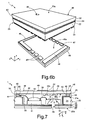
- Figure 3b shows only a portion of the aforesaid cap layers 20, 21, for providing a single MEMS device, it being, however, evident that a plurality of MEMS devices, set side-by-side, are provided by means of the same processing steps (so that, for example, several cavities 24 are made through the second cap layer 21 in this step, set at a distance apart from one another by an appropriate pitch, according to the final dimensions that the individual MEMS devices are to assume after the final cutting or "singulation" operation).
- first and second cap layers 20, 21 are joined together, in a stacked way (the so-called “stacking operation"), via the interposition, between the corresponding surfaces in contact (in areas corresponding to the respective second main faces 20b, 21b), of the adhesive layer 23 (the so-called “bonding operation”), forming in this way a composite cap 25.
- a seed layer 26 is grown, constituted by a thin metal film, on the top delimitation surface 24a of the cavity 24, on the side walls, designated by 24b, of the same cavity 24 and moreover on the first metal layer 22 in a region corresponding to the first main face 21a of the first cap layer 21.
- a second metal layer 28 which coats, in particular, the inside of the cavity 24.
- an acoustic access port 29 is provided, using micromachining techniques of a standard type, through the entire thickness of the first cap layer 20 and through the first metal layer 22, the seed layer 26 and the second metal layer 28.
- the acoustic access port 29 is, for example, constituted by a through hole with circular cross section extending from the first main face 20a of the first cap layer 20 as far as the cavity 24.
- the acoustic access port 29 is designed to enable entry of acoustic pressure waves into the package of the MEMS acoustic transducer.
- marking of the package can advantageously be carried out, for example for providing information regarding the manufacturing lot; in particular, marking can be carried out on the first main face 20a of the first cap layer 20, which is in fact accessible for the marking tools.
- the composite cap 25 is turned upside down along a vertical direction, and, via standard cutting processes (the so-called “sawing” operation), for example using a diamond-saw cutting tool, the second metal layer 28 is appropriately processed, for providing, at the first surface 21a of the second cap layer 21, a plurality of cavity contact pads or lands, denoted with 30 and referred to as "CCLs" (cavity-connect lands), electrically insulated from one another.
- standard cutting processes the so-called "sawing” operation
- the second metal layer 28 is appropriately processed, for providing, at the first surface 21a of the second cap layer 21, a plurality of cavity contact pads or lands, denoted with 30 and referred to as "CCLs" (cavity-connect lands), electrically insulated from one another.
- CCLs cavity-connect lands
- the cavity-connect lands 30 are designed to be contacted electrically, in particular using the wire-bonding technique, by electrical components that will subsequently be coupled to the composite cap 25, in an area corresponding to the top delimitation surface 24a of the cavity 24.
- an outer groove 32 having a perimeter substantially rectangular in the horizontal plane xy, which surrounds the cavity 24 at a given distance, and a depth such as to remove the second metal layer 28, the seed layer 26, the first metal layer 22, and a surface portion of the second cap layer 21 (at the corresponding first main face 21a); and a first inner groove 33 and a second inner groove 34, which extend inside the outer groove 32, at the side walls 24b of the cavity 24, and have substantially the same depth as the same outer groove 32.
- first and second inner grooves 33, 34 extend parallel to one another along respective major sides of the cavity 24 (in the example shown in Figure 4 , along the axis y), extending in part through a surface portion of the second cap layer 21, at the edge between the first main face 21a of the second cap layer 21 and the side walls 24b of the cavity 24. Consequently, two parallel strips of metal material are defined between the outer groove 32 and the first and second inner grooves 33, 34, the strips being electrically insulated from the coating layer inside the cavity 24, on account of the presence of the same first and second inner grooves 33, 34.
- a plurality of recesses 35 are moreover cut, having for example the same depth as the grooves 32, 33, 34, and extending in a direction transverse to, and starting from, the outer groove 32, as far as the first inner groove 33 or, respectively, the second inner groove 34 (hence traversing entirely the aforesaid parallel strips of metal material).
- the recesses 35 thus define, between them, the cavity-connect lands 30, which are electrically insulated from one another and moreover insulated with respect to the remaining portions of the second metal layer 28 (which remain at the side walls 24b of the cavity 24 and at the first main face 21a of the second cap layer 21, around the same cavity 24).
- three cavity-connect lands 30 may be provided, in a region corresponding to an end portion of each major side of the cavity 24.
- the depth of cut, the shape, number, and positioning of the various cavity-connect lands 30 can vary with respect to what is illustrated, for example in such a way as to be optimized with respect to the electrical connection requirements and characteristics of the MEMS acoustic transducer.
- a first die designated once again by 10, which integrates the micromechanical sensing structure (shown schematically, and provided, by way of non-limiting example, as described previously with reference to Figure 1 )
- a second die designated once again by 11, integrating an ASIC of the corresponding reading electronics, are coupled to the composite cap 25 at the top delimitation surface 24a of the cavity 24.
- a bottom surface 10a, 11a of both of the dice 10, 11 is glued by means of adhesive material to the second metal layer 28 in an area corresponding to the top delimitation surface 24a of the cavity 24.
- the first die 10 is positioned with respect to the composite cap 25 in such a way that the cavity 3 of the corresponding micromechanical sensing structure faces and is in fluid communication with the acoustic access port 29 so that the cavity 3 constitutes the front chamber of the MEMS acoustic transducer.
- first electrical wires 39 between the first contact pads 36 and the second contact pads 38a in such a way as to convey the electrical quantities detected by the micromechanical sensing structure towards the ASIC
- second electrical wires 40 between the third contact pads 38b and respective cavity-connect lands 30 in such a way as to enable, as will be described hereinafter, carrying the electrical signals generated by the ASIC to the outside of the package or else to further electrical/electronic components present inside the same package.
- a coating region 42 (the so-called "glob top” region), made of appropriate material, can be formed, optionally, on the top surface 11b of the second die 11 in such a way as to shield the ASIC from light radiation at spurious wavelengths, which are not blocked by the material of the composite cap 25 and by the material (typically silicon) of which the membrane 4 and the back plate 5 of the micromechanical sensing structure are made.
- the membrane 4 and the back plate 5 act as an interface between the outside of the package (in particular, the environment external to the acoustic access port 29) and the cavity 24 inside the same package.
- a thin film of an appropriate protective material can be formed, which performs the same function of shielding the light radiation.
- a sealing material for example, a conductive resin
- the sealing region 44 also constitutes an attachment base for coupling to a PCB (printed-circuit board) of a standard type.
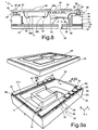
- the assembly process proceeds with coupling of a printed-circuit substrate 45 to the composite cap 25 in an area corresponding to the first main face 21a of the second cap layer 21 so as to close at the bottom (with respect to vertical axis z) the cavity 24 that is to constitute the back chamber of the MEMS acoustic transducer, here designated once again by 1.
- the printed-circuit substrate 45 has a first main face 45a set facing the inside of the cavity 24, and a second main face 45b set facing the outside of the package of the MEMS acoustic transducer 1, here designated as a whole by 46.
- first main face 45a Provided on the first main face 45a (see in particular Figure 6b ) are: substrate contact pads 47, made of metal material, for example in a number and with an arrangement corresponding to those of the cavity-connect lands 30; and conductive strips 48, having shapes and an arrangement such as to superimpose (as is evident from Figures 6a and 6b ) on the aforesaid remaining portions of the second metal layer 28 in an area corresponding to the first main face 21a of the second cap layer 21, providing an electrical contact with the same portions.
- connection paths, metallized vias, and/or further electrical-connection elements are moreover provided on the aforesaid first main face 45a and/or inside the same printed-circuit substrate 45.
- elements for electrical connection towards the outside are provided on the second main face 45b of the printed-circuit substrate 45, in particular for connection to a printed circuit board (or other support), to which the MEMS acoustic transducer is to be coupled.
- these electrical-connection elements are constituted by external contact pads 49 (connection with the LGA technique), which are appropriately connected (for example, by the metallized vias traversing the printed-circuit substrate 45) to the substrate contact pads 47 and/or the conductive strips 48.
- solder-paste regions 50 are pre-applied in appropriate areas on the first main face 45a of the printed-circuit substrate 45, for example in areas corresponding to the substrate contact pads 47 and/or the conductive strips 48.
- the solder-paste regions 50 can be applied using the screen-printing technique, or pre-applied during production of the printed-circuit substrate 45.
- the printed-circuit substrate 45 is positioned, using the flip-chip technique, with the first main face 45a facing the first main face 21a of the second cap layer 21 (in particular exploiting the resting base offered by the sealant region 44) in such a way that the substrate contact pads 47 are positioned at the cavity-connect lands 30.
- the stacked assembly of the printed-circuit substrate 45 and the composite cap 25 is subjected to brazing (the so-called "reflow” operation), in such a way as to obtain their mechanical and electrical bonding, by soldering.
- the package 46 is formed and the back chamber of the MEMS acoustic transducer 1 (constituted by the cavity 24 internal to the package 46) is defined, which is thus sealed from the external environment and also shielded from electromagnetic disturbance.
- the ASIC in the second die 11 of the MEMS acoustic transducer 1 is, at the end of the aforesaid stacked assembly, automatically connected by means of the electrical connections described to the substrate contact pads 47, and, consequently, to the external contact pads 49 for connection towards the outside of the package 46.
- the solder-paste regions 50 are located beside the sealing region 44, within the package 46.
- the various MEMS acoustic transducers 1 (and the corresponding packages 46) are singulated.
- the finished devices are then subjected to the usual testing procedures (for the so-called "sorting" operation).
- the shielding effect provided by the composite cap 25 in regard to the cavity 24 is enhanced as compared to traditional structures, thanks to the fact that two layers of the same material (first and second cap layers 20, 21) are coupled together and to the fact that the inside of the same cavity 24 is uniformly coated with one and the same layer of conductive material (the second metal layer 28).
- the use of the sealing region 44, of conductive material, for coupling between the composite cap 25 and the printed-circuit substrate 45 enables improved shielding against electromagnetic disturbance and also provision of a good ground connection.
- the definition of the cavity-connect lands 30 when providing the composite cap 25, using traditional cutting techniques advantageously enables different conductive patterns and electrical-connection pads to be obtained on the portions of the first main face 21a of the second cap layer 21 adjacent to the cavity 24, for connection to the printed-circuit substrate 45 during assembly of the package 46.
- the front chamber 27 of the MEMS acoustic transducer is in this case constituted by just the cavity 3 of the corresponding micromechanical sensing structure, and can consequently be controlled via an appropriate design of the micromechanical reduced volumes of the front chamber.
- This solution also renders the assembly process more robust given that the volume of the front chamber does not depend upon the realization and proper positioning of the components within the cavity 24.
- the volume of the back chamber is represented by the entire cavity 24, internal to the package 46, so that the upper limit for this volume is represented only by the external dimensions of the package 46, which can easily be defined at the design stage.
- the characteristics of the back chamber are linked principally to the structure of the package 46, it is possible to obtain micromechanical sensing structures of small dimensions (for example, using thinner silicon wafers as starting structural layers).
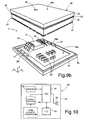
- a different embodiment of the present invention envisages the possibility that further electrical components 52, for example SMDs (surface-mounted devices), are coupled, in a known way, to the first main face 45a of the printed-circuit substrate 45.
- the electrical components 52 can be resistors, capacitors, or other active or passive components.
- further packages of electronic devices such as full-moulded or premoulded packages can be arranged inside the cavity 24 (by means of coupling to the first main face 45a of the printed-circuit substrate 45).
- the possibility of exploiting the first main face 45a of the printed-circuit substrate 45 (to which in this case the dice of the MEMS acoustic transducer are not coupled) for connection of further electrical/electronic components advantageously enables maximization of the space occupied inside the cavity 24, in this way reducing the occupation of area on the external printed circuit board to which the package 46 of the MEMS acoustic transducer 1 is coupled. Furthermore, this solution guarantees that all the electrical components 52 inside the package 46 are adequately shielded from EMI disturbance, since they are arranged inside the cavity 24, which is in turn totally shielded. It is to be noted that in the embodiment illustrated, the electrical components 52 are, at least in part, vertically set on top of the first die 10 inside the package 46.
- the electrical components 52 can be electrically connected to the ASIC integrated in the second die 11, through the cavity-connect lands 30, the second electrical wires 40, the solder-paste regions 50, the substrate contact pads 47, and appropriate electrical paths (or similar electrical connections) integrated in the printed-circuit substrate 45.
- the electrical components 52 are connected to the outside of the package through the external contact pads 49 and, again, electrical paths (or other electrical connections) in the printed-circuit substrate 45.
- FIG. 8 envisages that the second die 11 (integrating the ASIC) is coupled, with traditional techniques, to the first main face 45a of the printed-circuit substrate 45, together with the possible further electrical components 52.
- the first electrical wires 39 are connected inside the package 46 between the first contact pads 36 and the cavity-connect lands 30, whilst the second electrical wires 40 connect the second contact pads 38a (which define input pads) with the substrate contact pads 47 (for receiving the electrical quantities generated by the micromechanical sensing structure), and further second electrical wires, which are also designated by 40, connect the third contact pads 38b (which define output pads) to the external contact pads 49 and/or to the further electrical components 52.
- This solution can possibly enable a saving in the occupation of area in the horizontal plane xy inside the package 46.
- the assembly described enables convenient tuning of the volumes of the front and back chambers of the MEMS acoustic transducer 1 and achievement of high electrical performance of the transducer in terms, for example, of the frequency response and of the signal-to-noise ratio (SNR).
- SNR signal-to-noise ratio
- the described process makes it possible to carry out marking of the package 46 in an initial step thereof, thus enabling elimination of the risk of contamination by dust or by external agents of the MEMS acoustic transducer 1 (which in the initial step has not yet been coupled to the structure being assembled).
- the layout proposed for the package 46 of the MEMS acoustic transducer 1 moreover minimizes exposure of the electrical/electronic components inside the cavity 24 to light radiation, given that light radiation is largely absorbed by the micromechanical sensing structure integrated in the first die 10, which is set between the acoustic access port 29 and the inside of the cavity 24.
- the electrical wire connections inside the cavity 24, in particular for connection between the first and second dice 10, 11, are better protected from the outside environment, as compared to traditional package solutions (of the same "top port" type).
- the mechanical robustness of the assembly is in general improved, given that the micromechanical sensing structure (integrated in the first die 10) is attached to the composite cap 25 in an area corresponding to its internal surface opposite to the printed-circuit substrate 45 (the top delimitation surface 24a of the cavity 24) so that the sturdiness and strength at drop tests are improved.
- the characteristics previously listed render the use of the MEMS acoustic transducer 1 particularly advantageous in an electronic device 60, as shown in Figure 10 .
- the electronic device 60 is preferably a mobile communications device, such as, for example, a cellphone, a PDA, a notebook, but also a voice recorder, an audio-file reader with voice-recording capacity, etc.
- the electronic device 60 may be a hydrophone, capable of working under water, or else a hearing-aid device.
- the electronic device 60 comprises a microprocessor (CPU - central processing unit) 61, a memory block 62, connected to the microprocessor 61, and an input/output interface 63, for example provided with a keyboard and a display, which is also connected to the microprocessor 61.
- the MEMS acoustic transducer 1 communicates with the microprocessor 61.
- the ASIC in the second die 11 sends electrical output signals to the microprocessor 61 (a further electronic circuit for processing these electrical output signals, designated by 65, may possibly be present).
- a loudspeaker 66 is also provided for generation of sounds on an audio output (not shown) of the electronic device 60.
- the MEMS acoustic transducer 1 As shown schematically, the MEMS acoustic transducer 1, the microprocessor 61, the memory block 62, the input/output interface 63, and the possible further electronic components are coupled to a single printed circuit board 67, for example using the SMD technique.
- the assembly proposed can advantageously be used also for other types of MEMS transducers and corresponding packages, envisaging the presence of an access port enabling fluid communication between the external environment and the inside of the package.
Description
- The present invention relates to a transducer of a MEMS (Micro-Electro-Mechanical System) type, in particular a capacitive microphone, to which the ensuing treatment will make explicit reference, without this implying any loss of generality, and to a corresponding assembly process.
- As it is usual in this technical field, the term "package" will be used herein to designate, as a whole, the casing, or covering structure, which surrounds, completely or partially, the die or dice of semiconductor material constituting the acoustic transducer, enabling electrical connection thereof to the outside (in particular, connection to a printed circuit of a corresponding electronic device).
- As is known, an acoustic transducer, for example a MEMS microphone of a capacitive type, generally comprises a micromechanical sensing structure, designed to transduce acoustic pressure waves into an electrical quantity (in particular a capacitive variation), and reading electronics, designed to carry out appropriate processing operations (amongst which amplification and filtering operations) of this electrical quantity for supplying an electrical output signal (for example, a voltage).
- The micromechanical sensing structure in general comprises a mobile electrode, provided as a diaphragm or membrane, set facing a fixed electrode, at a short distance of separation (gap), to provide the plates of a sensing capacitor with a capacitance that varies as a function of the acoustic pressure waves to be detected. The mobile electrode is generally anchored, by means of a perimetral portion thereof, to a fixed structure, whilst a central portion thereof is free to move, or undergo deformation, in response to the pressure exerted by the incident acoustic pressure waves, in this way causing a capacitance variation of the sensing capacitor.
- In greater detail, and with reference to
Figure 1 , a micromechanical sensing structure of a MEMSacoustic transducer 1, of a known type, comprises astructural layer 2 of semiconductor material, for example silicon, in which acavity 3 is provided, for example via chemical etching from the back. A membrane, or diaphragm, 4 is coupled to thestructural layer 2 and closes thecavity 3 at the top; themembrane 4 is flexible and, in use, undergoes deformation as a function of the pressure of the incident sound waves. A rigid plate 5 (generally referred to as "back-plate") is set above themembrane 4 and faces it, via the interposition of spacers 6 (for example, made of insulating material, such as silicon oxide). Theback plate 5 constitutes the fixed electrode of a sensing capacitor with a variable capacitance, the mobile electrode of which is constituted by themembrane 4, and has a plurality ofholes 7, designed to enable the circulation of air towards the membrane 4 (rendering theback plate 5 acoustically transparent). The micromechanical sensing structure further comprises (in a way not illustrated) membrane and back-plate electrical contacts, used for biasing themembrane 4 and theback plate 5 and detecting a signal of capacitive variation resulting from the deformation of themembrane 4 caused by the incident acoustic pressure waves; in general, these electrical contacts are arranged in a surface portion of the die, in which the micromechanical sensing structure is provided. - In a known way, the sensitivity of the MEMS
acoustic transducer 1 depends on the mechanical characteristics of themembrane 4 of the micromechanical sensing structure (in particular upon its so-called "mechanical compliance") and on the type of assembly of themembrane 4 andback plate 5. - In addition, the volume of the front acoustic chamber or simply "front chamber" (i.e., the space traversed in use by acoustic pressure waves coming from the external environment through an appropriate access port), and the volume of the back acoustic chamber, or "back-chamber" (i.e., the space that is located on the opposite side of the front chamber with respect to the
membrane 4, set in use at a reference pressure) directly affect the acoustic performance of the transducer. - In particular, the volume of the front chamber behaves as a sort of Helmholtz resonator, on account of the oscillations of the air penetrating through the access port. In fact, the acoustic input signal causes an increase in the pressure of the air inside the front chamber, which consequently acts as a spring pushing out air from the same chamber. As a result of the forces of inertia of the air mass leaving the front chamber, the increase of pressure inside the same chamber is over-compensated, causing a pressure drop, and the negative pressure that is created in the front chamber attracts new air therein. This repeated change of pressure generates the oscillations of air inside the front chamber, at a given resonance frequency. The volume of the front chamber is such as to determine the upper resonance frequency of the acoustic transducer, and hence its performance for high frequencies (in fact, the operative frequency band of the acoustic transducer has to be lower than the resonance frequency of the oscillations of the air): in general, the smaller the volume of the front chamber, the higher the upper cut-off frequency of the transducer in so far as the resonance frequency of the oscillations of air shifts towards higher frequencies.
- The back chamber behaves, instead, as a closed volume subject to compression, with the consequence that the smaller the volume of the back chamber, the lower the sensitivity of the acoustic transducer (in fact, it is as if the deformations of the membrane were hindered by the action of a high-stiffness spring). It is hence generally desirable to provide a back chamber of large dimensions so as to improve the sensitivity of the acoustic transducer.
- The volume of the front chamber and/or of the back chamber of the MEMS acoustic transducer not only depend upon the configuration of the micromechanical sensing structure, but also upon the conformation of the corresponding package, which has to be configured so as to house not only the same micromechanical sensing structure, but also the reading electronics associated thereto, generally provided as an ASIC in a respective die of semiconductor material.
- In the design stage, it has also to be considered that the presence of acoustic access ports, directly communicating with the external environment, designed to enable entry of the acoustic pressure waves towards the
membrane 4 of the micromechanical sensing structure, involves the further requirement of pre-arranging appropriate shields for the incident light, which could jeopardize proper operation of the micromechanical sensing structure and of the reading electronics. - Several constraints are thus imposed on the assembly of a MEMS acoustic transducer (and of the corresponding package), which render design thereof particularly problematical, especially where compact dimensions and high electrical and mechanical performance are called for.
- In a known assembly arrangement, represented schematically in
Figure 2 , afirst die 10, integrating the micromechanical sensing structure (here only shown schematically), and asecond die 11, integrating the ASIC of the corresponding reading electronics, are coupled side-by-side on asubstrate 12.Electrical connections 15 between the first andsecond dice second die 11 and thesubstrate 12, are provided with the wire-bonding technique (i.e., with appropriate electrical wires), whilst metallization layers and vias (not shown in detail) are provided through thesubstrate 12 for routing the electrical signals towards the outside of the package of the MEMS acoustic transducer, which is once again designated as a whole by 1. In a way not illustrated, pads (in the case of an LGA - Land-Grid Array - package), or conductive spherical elements (in the case of a BGA - Ball-Grid Array - package), or similar connection elements, are moreover provided on the underside of thesubstrate 12 for soldering and electrical connection to an external printed circuit of a corresponding electronic device. - A
cap 16 is coupled to thesubstrate 12, and encloses within it the first andsecond dice cap 16 may be made of metal, or of a pre-moulded plastic coated within with a metallization layer, in such a way as to prevent disturbance due to external electromagnetic signals (by providing a sort of Faraday cage). Thecap 16 is generally attached to thesubstrate 12 by means of a conductive glue 17 (for example, epoxy resin) so as to obtain also a ground connection towards thesubstrate 12. Thecap 16 further has anopening 18 to enable entry into the package of acoustic pressure waves coming from the external environment. - The above solution is not however free from drawbacks. In particular, the
cap 16 is made through moulding and hence requires, during production, a set of specific and dedicated moulding tools (comprising, for example, dies and punches), for each possible variation of dimensions and shapes that may prove necessary in time, for example following upon the evolution of the dimensions of the silicon structures or upon specific requirements of the end user. In addition, the pitch and layout of the moulding and punching tools are not always compatible with the dimensions and configuration of the array of contacts (for example, of an MAP-BGA - Mould-Array Process - Ball-Grid Array - type) each time used for MEMS devices. The production and fixing of thecap 16 to thesubstrate 12 cannot hence be obtained with technologies and equipment for so-called "mass production". - The above solution involves large dimensions for accommodating side-by-side the two dice of the MEMS acoustic transducer and for providing the corresponding package, and in general has the disadvantage of not offering to the designer a sufficient freedom (as instead would be desirable) in the sizing of the front and back chambers of the acoustic transducer, for determination of its electrical characteristics. Moreover, in general, providing the
electrical connections 15, in particular towards the substrate of the package, can prove problematical in the flow of the assembly process. -
WO/2007 022249 discloses an apparatus having a package, with a base and a lid coupled with the package base. The lid and package base form a chamber for at least partially containing a microphone. The lid is electrically coupled with a given portion of the leadframe in the package base. - The aim of the present invention is to provide an appropriate assembly of a MEMS acoustic transducer and of a corresponding package, which will enable solution of the problems highlighted above, and in particular enable reduced manufacturing costs, high acoustic performance and reliability, and small dimensions.
- According to the present invention, a transducer of a microelectromechanical type and a corresponding assembly process are provided, as defined in
claims 1 and 13, respectively. - For a better understanding of the present invention, a preferred embodiment thereof is now described, purely by way of non-limiting example and with reference to the attached drawings, wherein:
-
Figure 1 is a schematic cross section of a micromechanical sensing structure of a MEMS acoustic transducer, of a known type; -
Figure 2 is a schematic cross section of a MEMS acoustic transducer and of the corresponding package, of a known type; -
Figures 3a-3g show cross sections through a MEMS acoustic transducer, in successive steps of the corresponding assembly process, according to one embodiment of the present invention; -
Figure 4 is a perspective schematic view of the transducer ofFigure 3d , which moreover shows the (broken) line of cross section along which the representation ofFigure 3d is obtained; -
Figure 5 is a perspective view of the transducer ofFigure 3e , which again shows the (broken) line of cross section along which the representation ofFigure 3e is obtained; -
Figures 6a ,6b are schematic perspective views, respectively, from above and from beneath, partially in cutaway view, of the MEMS acoustic transducer ofFigure 3g ; -
Figure 7 is a cross-sectional view similar to that ofFigure 3g , regarding a different embodiment of the present invention; -
Figure 8 is a cross-sectional view similar to that ofFigure 3g , regarding yet another different embodiment of the present invention; -
Figures 9a ,9b are schematic perspective views, respectively, from above and from beneath, of the MEMS acoustic transducer ofFigure 8 (Figure 9a shows the broken line of cross section along which the representation ofFigure 8 is obtained); and -
Figure 10 shows a general block diagram of an electronic device incorporating the MEMS acoustic transducer according to a further aspect of the present invention. - As will be discussed in detail in what follows, one aspect of the present invention envisages providing a specific cap structure for the package of a MEMS acoustic transducer, of a composite type, constituted by the assembly of two layers made of a same plastic material, obtained with standard semiconductor techniques (such as standard techniques for obtaining BGA, LGA substrates, or the like). In addition, one or both of the dice of the MEMS acoustic transducer (integrating the micromechanical sensing structure and, respectively, the corresponding ASIC), and/or further electrical/electronic components, are directly coupled to the cap structure, instead of being coupled to a substrate to which the same cap structure is bonded for providing the package of the MEMS acoustic transducer and its connection to an external printed circuit board.
- In detail, and with reference firstly to
Figure 3a , a process of assembly of a MEMS acoustic transducer initially envisages providing afirst cap layer 20 and asecond cap layer 21, made of one and the same plastic material, in particular an epoxy resin, and specifically a laminated BT (bismaleimide triazine). - The
first cap layer 20 has a firstmain face 20a and a secondmain face 20b (where by "main faces" is meant the surfaces of greater extension of the layer, in a horizontal plane xy), and a first thickness along a vertical axis z, transverse to the horizontal plane xy. In particular, the firstmain face 20a, as will be clarified hereinafter, is designed to define the upper face of the package of the MEMS acoustic transducer (in the so-called "top port" configuration, i.e., with a corresponding acoustic access port facing in the opposite direction with respect to the printed circuit board to which the MEMS acoustic transducer is designed to be coupled). Thesecond cap layer 21 has, in turn, a respective firstmain face 21a and a respective secondmain face 21b, and a second thickness, greater than the first thickness of thefirst cap layer 20. In particular, the second thickness is a function, for reasons that will be clarified hereinafter, of the vertical dimensions of the dice of the MEMS acoustic transducer (integrating, as previously underlined, the micromechanical sensing structure and the corresponding ASIC). - The main faces of the
first cap layer 20 and of thesecond cap layer 21 are coated, with techniques of a standard type, by a thin first metal layer 22 (as shown inFigure 3a , the firstmain face 20a of thefirst cap layer 20, designed to define the outer surface of the package, may not be metallized). In addition, anadhesion layer 23, of non-conductive adhesive material, is formed on thefirst metal layer 22 in a region corresponding to the secondmain face 21b of thesecond cap layer 21. - Then (see
Figure 3b ), acavity 24 is provided through thesecond cap layer 21, traversing it throughout its thickness and moreover traversing the first metal layer 22 (in regions corresponding to both of itsmain faces adhesive layer 23. In a way here not illustrated, thecavity 24 has, for example, a rectangular shape in plan view (in the horizontal plane xy) and, for the reasons that will be clarified hereinafter, dimensions such as to accommodate within it one or both of the dice of the micromechanical sensing structure and of the ASIC of the MEMS acoustic transducer. - Note that
Figure 3b , as likewise the subsequent ones (unless otherwise indicated), show only a portion of the aforesaid cap layers 20, 21, for providing a single MEMS device, it being, however, evident that a plurality of MEMS devices, set side-by-side, are provided by means of the same processing steps (so that, for example,several cavities 24 are made through thesecond cap layer 21 in this step, set at a distance apart from one another by an appropriate pitch, according to the final dimensions that the individual MEMS devices are to assume after the final cutting or "singulation" operation). Next, the first and second cap layers 20, 21 are joined together, in a stacked way (the so-called "stacking operation"), via the interposition, between the corresponding surfaces in contact (in areas corresponding to the respective secondmain faces composite cap 25. Thefirst cap layer 20, and in particular the corresponding secondmain face 20b (with thefirst metal layer 22 superimposed thereon), constitutes atop delimitation surface 24a of thecavity 24, closing it at the top (considering that, as pointed out previously, thefirst cap layer 20a is designed to constitute the upper face of the package of the MEMS acoustic transducer, in a "top port" configuration). - Next, a
seed layer 26 is grown, constituted by a thin metal film, on thetop delimitation surface 24a of thecavity 24, on the side walls, designated by 24b, of thesame cavity 24 and moreover on thefirst metal layer 22 in a region corresponding to the firstmain face 21a of thefirst cap layer 21. Then, formed on theseed layer 26, for example using the electroplating technique or the sputtering technique, is asecond metal layer 28, which coats, in particular, the inside of thecavity 24. - Next (as shown in
Figure 3c ), anacoustic access port 29 is provided, using micromachining techniques of a standard type, through the entire thickness of thefirst cap layer 20 and through thefirst metal layer 22, theseed layer 26 and thesecond metal layer 28. Theacoustic access port 29 is, for example, constituted by a through hole with circular cross section extending from the firstmain face 20a of thefirst cap layer 20 as far as thecavity 24. As will be clarified hereinafter, theacoustic access port 29 is designed to enable entry of acoustic pressure waves into the package of the MEMS acoustic transducer. - In this step, in a way not illustrated, marking of the package can advantageously be carried out, for example for providing information regarding the manufacturing lot; in particular, marking can be carried out on the first
main face 20a of thefirst cap layer 20, which is in fact accessible for the marking tools. - According to one aspect of the present invention (see
Figure 3d , as well as the corresponding perspective view ofFigure 4 ), thecomposite cap 25 is turned upside down along a vertical direction, and, via standard cutting processes (the so-called "sawing" operation), for example using a diamond-saw cutting tool, thesecond metal layer 28 is appropriately processed, for providing, at thefirst surface 21a of thesecond cap layer 21, a plurality of cavity contact pads or lands, denoted with 30 and referred to as "CCLs" (cavity-connect lands), electrically insulated from one another. As will be clarified hereinafter, the cavity-connect lands 30 are designed to be contacted electrically, in particular using the wire-bonding technique, by electrical components that will subsequently be coupled to thecomposite cap 25, in an area corresponding to thetop delimitation surface 24a of thecavity 24. - In greater detail, during the aforesaid cutting operation, the following elements are defined by way of removal of material: an
outer groove 32, having a perimeter substantially rectangular in the horizontal plane xy, which surrounds thecavity 24 at a given distance, and a depth such as to remove thesecond metal layer 28, theseed layer 26, thefirst metal layer 22, and a surface portion of the second cap layer 21 (at the corresponding firstmain face 21a); and a firstinner groove 33 and a secondinner groove 34, which extend inside theouter groove 32, at theside walls 24b of thecavity 24, and have substantially the same depth as the sameouter groove 32. In particular, the first and secondinner grooves Figure 4 , along the axis y), extending in part through a surface portion of thesecond cap layer 21, at the edge between the firstmain face 21a of thesecond cap layer 21 and theside walls 24b of thecavity 24. Consequently, two parallel strips of metal material are defined between theouter groove 32 and the first and secondinner grooves cavity 24, on account of the presence of the same first and secondinner grooves - During the sawing operation, a plurality of recesses 35 (visible in
Figure 4 ) are moreover cut, having for example the same depth as thegrooves outer groove 32, as far as the firstinner groove 33 or, respectively, the second inner groove 34 (hence traversing entirely the aforesaid parallel strips of metal material). In particular, therecesses 35 thus define, between them, the cavity-connect lands 30, which are electrically insulated from one another and moreover insulated with respect to the remaining portions of the second metal layer 28 (which remain at theside walls 24b of thecavity 24 and at the firstmain face 21a of thesecond cap layer 21, around the same cavity 24). - For example, as may be seen in
Figure 4 , three cavity-connect lands 30 may be provided, in a region corresponding to an end portion of each major side of thecavity 24. In any case, it is emphasized that the depth of cut, the shape, number, and positioning of the various cavity-connect lands 30 can vary with respect to what is illustrated, for example in such a way as to be optimized with respect to the electrical connection requirements and characteristics of the MEMS acoustic transducer. - After the sawing operation (see
Figure 3e and the correspondingFigure 5 ), a first die, designated once again by 10, which integrates the micromechanical sensing structure (shown schematically, and provided, by way of non-limiting example, as described previously with reference toFigure 1 ), and a second die, designated once again by 11, integrating an ASIC of the corresponding reading electronics, are coupled to thecomposite cap 25 at thetop delimitation surface 24a of thecavity 24. In particular, abottom surface dice second metal layer 28 in an area corresponding to thetop delimitation surface 24a of thecavity 24.First contact pads 36 associated to themembrane 4 and to the back plate 5 (here illustrated schematically) of the micromechanical sensing structure integrated in thefirst die 10, carried by atop surface 10b thereof, and moreover second andthird contact pads second die 11, carried by a respectivetop surface 11b thereof, instead face the horizontal plane (parallel to the plane xy) defined by the firstmain face 21a of thesecond cap layer 21. - In addition, the
first die 10 is positioned with respect to thecomposite cap 25 in such a way that thecavity 3 of the corresponding micromechanical sensing structure faces and is in fluid communication with theacoustic access port 29 so that thecavity 3 constitutes the front chamber of the MEMS acoustic transducer. - The electrical connections to/from the first and
second dice electrical wires 39 between thefirst contact pads 36 and thesecond contact pads 38a (in such a way as to convey the electrical quantities detected by the micromechanical sensing structure towards the ASIC); and, according to one aspect of the present invention, secondelectrical wires 40 between thethird contact pads 38b and respective cavity-connect lands 30 (in such a way as to enable, as will be described hereinafter, carrying the electrical signals generated by the ASIC to the outside of the package or else to further electrical/electronic components present inside the same package). - As shown schematically only in
Figure 3e , a coating region 42 (the so-called "glob top" region), made of appropriate material, can be formed, optionally, on thetop surface 11b of thesecond die 11 in such a way as to shield the ASIC from light radiation at spurious wavelengths, which are not blocked by the material of thecomposite cap 25 and by the material (typically silicon) of which themembrane 4 and theback plate 5 of the micromechanical sensing structure are made. In this regard, it should in fact be noted that in the package structure proposed, themembrane 4 and theback plate 5 act as an interface between the outside of the package (in particular, the environment external to the acoustic access port 29) and thecavity 24 inside the same package. Alternatively, on thetop surface 11b of the second die 11 a thin film of an appropriate protective material can be formed, which performs the same function of shielding the light radiation. - Next (see
Figure 3f where, by way of example, portions of two MEMS devices set side-by-side, obtained starting from the same layers, are shown), a sealing material (for example, a conductive resin) is distributed along what will be, after the final singulation operation, the perimeter of each MEMS device, and in particular inside theouter groove 32, thus creating therein a sealingregion 44. In particular, the sealingregion 44 also constitutes an attachment base for coupling to a PCB (printed-circuit board) of a standard type. - In this regard (see
Figure 3g and the correspondingFigures 6a and6b ), the assembly process proceeds with coupling of a printed-circuit substrate 45 to thecomposite cap 25 in an area corresponding to the firstmain face 21a of thesecond cap layer 21 so as to close at the bottom (with respect to vertical axis z) thecavity 24 that is to constitute the back chamber of the MEMS acoustic transducer, here designated once again by 1. The printed-circuit substrate 45 has a firstmain face 45a set facing the inside of thecavity 24, and a secondmain face 45b set facing the outside of the package of the MEMSacoustic transducer 1, here designated as a whole by 46. - Provided on the first
main face 45a (see in particularFigure 6b ) are:substrate contact pads 47, made of metal material, for example in a number and with an arrangement corresponding to those of the cavity-connect lands 30; andconductive strips 48, having shapes and an arrangement such as to superimpose (as is evident fromFigures 6a and6b ) on the aforesaid remaining portions of thesecond metal layer 28 in an area corresponding to the firstmain face 21a of thesecond cap layer 21, providing an electrical contact with the same portions. In a way not illustrated, on the aforesaid firstmain face 45a and/or inside the same printed-circuit substrate 45, connection paths, metallized vias, and/or further electrical-connection elements are moreover provided. - Instead, elements for electrical connection towards the outside are provided on the second
main face 45b of the printed-circuit substrate 45, in particular for connection to a printed circuit board (or other support), to which the MEMS acoustic transducer is to be coupled. In the case illustrated, these electrical-connection elements are constituted by external contact pads 49 (connection with the LGA technique), which are appropriately connected (for example, by the metallized vias traversing the printed-circuit substrate 45) to thesubstrate contact pads 47 and/or the conductive strips 48. - In greater detail, and as illustrated in
Figure 3g , solder-paste regions 50 are pre-applied in appropriate areas on the firstmain face 45a of the printed-circuit substrate 45, for example in areas corresponding to thesubstrate contact pads 47 and/or the conductive strips 48. The solder-paste regions 50 can be applied using the screen-printing technique, or pre-applied during production of the printed-circuit substrate 45. Then, the printed-circuit substrate 45 is positioned, using the flip-chip technique, with the firstmain face 45a facing the firstmain face 21a of the second cap layer 21 (in particular exploiting the resting base offered by the sealant region 44) in such a way that thesubstrate contact pads 47 are positioned at the cavity-connect lands 30. At this point, the stacked assembly of the printed-circuit substrate 45 and thecomposite cap 25 is subjected to brazing (the so-called "reflow" operation), in such a way as to obtain their mechanical and electrical bonding, by soldering. Like this, thepackage 46 is formed and the back chamber of the MEMS acoustic transducer 1 (constituted by thecavity 24 internal to the package 46) is defined, which is thus sealed from the external environment and also shielded from electromagnetic disturbance. It may be noted that the ASIC in thesecond die 11 of the MEMSacoustic transducer 1 is, at the end of the aforesaid stacked assembly, automatically connected by means of the electrical connections described to thesubstrate contact pads 47, and, consequently, to theexternal contact pads 49 for connection towards the outside of thepackage 46. In particular, once assembly is completed, the solder-paste regions 50 are located beside the sealingregion 44, within thepackage 46. - Finally, using traditional cutting techniques, the various MEMS acoustic transducers 1 (and the corresponding packages 46) are singulated. The finished devices are then subjected to the usual testing procedures (for the so-called "sorting" operation).
- In the final structure of the
package 46, the shielding effect provided by thecomposite cap 25 in regard to thecavity 24 is enhanced as compared to traditional structures, thanks to the fact that two layers of the same material (first and second cap layers 20, 21) are coupled together and to the fact that the inside of thesame cavity 24 is uniformly coated with one and the same layer of conductive material (the second metal layer 28). In addition, the use of the sealingregion 44, of conductive material, for coupling between thecomposite cap 25 and the printed-circuit substrate 45 enables improved shielding against electromagnetic disturbance and also provision of a good ground connection. - In particular, it may be noted that the definition of the cavity-
connect lands 30 when providing thecomposite cap 25, using traditional cutting techniques, advantageously enables different conductive patterns and electrical-connection pads to be obtained on the portions of the firstmain face 21a of thesecond cap layer 21 adjacent to thecavity 24, for connection to the printed-circuit substrate 45 during assembly of thepackage 46. This solution at the same time enables the following results to be obtained in a simplified manner: electrical connections, inside the package, between the first andsecond dice cavity 24 and are directly coupled to thecomposite cap 25, and the printed-circuit substrate 45 that is to be connected to external printed circuit boards; and acomposite cap 25 having a totally shieldedcavity 24 in such a way as to guarantee proper shielding against electromagnetic disturbance. - In addition, it is to be noted that, advantageously, the front chamber 27 of the MEMS acoustic transducer is in this case constituted by just the
cavity 3 of the corresponding micromechanical sensing structure, and can consequently be controlled via an appropriate design of the micromechanical reduced volumes of the front chamber. This solution also renders the assembly process more robust given that the volume of the front chamber does not depend upon the realization and proper positioning of the components within thecavity 24. - Instead, once again advantageously, the volume of the back chamber is represented by the
entire cavity 24, internal to thepackage 46, so that the upper limit for this volume is represented only by the external dimensions of thepackage 46, which can easily be defined at the design stage. In particular, given that the characteristics of the back chamber are linked principally to the structure of thepackage 46, it is possible to obtain micromechanical sensing structures of small dimensions (for example, using thinner silicon wafers as starting structural layers). - A different embodiment of the present invention (shown in
Figure 7 ) envisages the possibility that furtherelectrical components 52, for example SMDs (surface-mounted devices), are coupled, in a known way, to the firstmain face 45a of the printed-circuit substrate 45. For example, theelectrical components 52 can be resistors, capacitors, or other active or passive components. Moreover, in this way, also further packages of electronic devices, such as full-moulded or premoulded packages can be arranged inside the cavity 24 (by means of coupling to the firstmain face 45a of the printed-circuit substrate 45). - Generally, the possibility of exploiting the first
main face 45a of the printed-circuit substrate 45 (to which in this case the dice of the MEMS acoustic transducer are not coupled) for connection of further electrical/electronic components advantageously enables maximization of the space occupied inside thecavity 24, in this way reducing the occupation of area on the external printed circuit board to which thepackage 46 of the MEMSacoustic transducer 1 is coupled. Furthermore, this solution guarantees that all theelectrical components 52 inside thepackage 46 are adequately shielded from EMI disturbance, since they are arranged inside thecavity 24, which is in turn totally shielded. It is to be noted that in the embodiment illustrated, theelectrical components 52 are, at least in part, vertically set on top of thefirst die 10 inside thepackage 46. Theelectrical components 52 can be electrically connected to the ASIC integrated in thesecond die 11, through the cavity-connect lands 30, the secondelectrical wires 40, the solder-paste regions 50, thesubstrate contact pads 47, and appropriate electrical paths (or similar electrical connections) integrated in the printed-circuit substrate 45. Alternatively, or in addition, theelectrical components 52 are connected to the outside of the package through theexternal contact pads 49 and, again, electrical paths (or other electrical connections) in the printed-circuit substrate 45. - Yet a further different embodiment of the present invention (shown in
Figure 8 and in the correspondingFigures 9a and9b ) envisages that the second die 11 (integrating the ASIC) is coupled, with traditional techniques, to the firstmain face 45a of the printed-circuit substrate 45, together with the possible furtherelectrical components 52. In this case, the firstelectrical wires 39 are connected inside thepackage 46 between thefirst contact pads 36 and the cavity-connect lands 30, whilst the secondelectrical wires 40 connect thesecond contact pads 38a (which define input pads) with the substrate contact pads 47 (for receiving the electrical quantities generated by the micromechanical sensing structure), and further second electrical wires, which are also designated by 40, connect thethird contact pads 38b (which define output pads) to theexternal contact pads 49 and/or to the furtherelectrical components 52. This solution can possibly enable a saving in the occupation of area in the horizontal plane xy inside thepackage 46. - The advantages of the MEMS acoustic transducer and of the corresponding assembly process emerge clearly from the foregoing description.
- In particular, it is once again emphasized that the use of a composite cap structure made of plastic material (in particular BT material) enables the use of traditional manufacturing techniques (mass-production techniques), without it being necessary to use specific moulding tools and machinery. It is in this way easy to adapt the process to different shapes or sizes of the package, without incurring in high costs for tooling.
- The assembly described enables convenient tuning of the volumes of the front and back chambers of the MEMS
acoustic transducer 1 and achievement of high electrical performance of the transducer in terms, for example, of the frequency response and of the signal-to-noise ratio (SNR). - Use of the cavity-connect lands 30, as previously emphasized, enables providing of the electrical connections inside (and towards the outside of) the
package 46 already during assembly of thecomposite cap 25, enabling the dual advantage of providing in a simple and inexpensive way, with the same processing steps, both the connections to the printed-circuit substrate 45 and a totally shieldedcavity 24 inside thepackage 46. - In addition, the described process makes it possible to carry out marking of the
package 46 in an initial step thereof, thus enabling elimination of the risk of contamination by dust or by external agents of the MEMS acoustic transducer 1 (which in the initial step has not yet been coupled to the structure being assembled). - The layout proposed for the
package 46 of the MEMSacoustic transducer 1 moreover minimizes exposure of the electrical/electronic components inside thecavity 24 to light radiation, given that light radiation is largely absorbed by the micromechanical sensing structure integrated in thefirst die 10, which is set between theacoustic access port 29 and the inside of thecavity 24. For the same reason, the electrical wire connections inside thecavity 24, in particular for connection between the first andsecond dice - Also the mechanical robustness of the assembly is in general improved, given that the micromechanical sensing structure (integrated in the first die 10) is attached to the
composite cap 25 in an area corresponding to its internal surface opposite to the printed-circuit substrate 45 (thetop delimitation surface 24a of the cavity 24) so that the sturdiness and strength at drop tests are improved. - The characteristics previously listed render the use of the MEMS
acoustic transducer 1 particularly advantageous in anelectronic device 60, as shown inFigure 10 . Theelectronic device 60 is preferably a mobile communications device, such as, for example, a cellphone, a PDA, a notebook, but also a voice recorder, an audio-file reader with voice-recording capacity, etc. Alternatively, theelectronic device 60 may be a hydrophone, capable of working under water, or else a hearing-aid device. - The
electronic device 60 comprises a microprocessor (CPU - central processing unit) 61, amemory block 62, connected to themicroprocessor 61, and an input/output interface 63, for example provided with a keyboard and a display, which is also connected to themicroprocessor 61. The MEMSacoustic transducer 1 communicates with themicroprocessor 61. In particular, the ASIC in thesecond die 11 sends electrical output signals to the microprocessor 61 (a further electronic circuit for processing these electrical output signals, designated by 65, may possibly be present). Aloudspeaker 66 is also provided for generation of sounds on an audio output (not shown) of theelectronic device 60. As shown schematically, the MEMSacoustic transducer 1, themicroprocessor 61, thememory block 62, the input/output interface 63, and the possible further electronic components are coupled to a single printedcircuit board 67, for example using the SMD technique. - Finally, it is clear that modifications and variations may be made to what has been described and illustrated herein, without thereby departing from the scope of the present invention, as defined in the attached claims.
- In particular, it is emphasized once again that, generally, the shapes and configurations of the structural elements described can be different from what has been described and illustrated so far, as likewise the electrical components that can be coupled inside the package may be different. For example, further electrical/electronic components could be appropriately coupled to the
composite cap 25, which can be electrically reached via the cavity-connect lands 30. - In addition, it is evident that the assembly proposed can advantageously be used also for other types of MEMS transducers and corresponding packages, envisaging the presence of an access port enabling fluid communication between the external environment and the inside of the package.
Claims (19)
- A MEMS transducer (1), comprising a micromechanical sensing structure (10) and a package (46), said package (46) being provided with a substrate (45), carrying first electrical-connection elements (47), and a lid (25), coupled to said substrate (45) to define an internal cavity (24), in which said micromechanical sensing structure (10) is housed, said lid (25) being formed by: a cap layer (20) having a first surface (20a) and a second surface (20b), which are set opposite to one another, said first surface (20a) defining an external face of said package (46) and said second surface (20b) facing said substrate (45) inside said package (46); and a wall structure (21), set between said cap layer (20) and said substrate (45), and having a coupling face (21a) coupled to said substrate (45),
characterized in that at least a first electrical component (10, 11) is coupled to said second surface (20b) of said cap layer (20), inside said package (46), and said coupling face (21a) of said wall structure (21) carries second electrical-connection elements (30), designed to electrically connect said first electrical component (10, 11) to said first electrical-connection elements (47). - The transducer according to claim 1, wherein said wall structure (21) delimits and surrounds said internal cavity (24) with corresponding wall surfaces (24b), and said second electrical-connection elements comprise cavity-connect lands (30), electrically insulated from one another and adjacent to said internal cavity (24).
- The transducer according to claim 2, wherein said cavity-connect lands (30) are connected to said first electrical-connection elements (47) by means of solder-paste regions (50), which are set between said coupling face (21a) and said substrate (45); further comprising a sealing region (44), made of conductive material, set between said wall structure (21) and said substrate (45), externally to said solder-paste regions (50) with respect to said cavity (24).
- The transducer according to any one of the preceding claims, wherein said cap layer (20) is traversed by an access port (29) designed to enable a fluid communication between the inside and the outside of said package (46), and said micromechanical sensing structure is integrated in a first die (10) coupled to said second surface (20b) of said cap layer (20), in an area corresponding to said access port (29); said micromechanical sensing structure (10) comprising a structural layer (2), a sensing cavity (3) formed in said structural layer (2), and a membrane (4), said sensing cavity (3) being in fluid communication with said access port (29) and said membrane (4) separating said sensing cavity (3) from said internal cavity (24).
- The transducer according to claim 4, of an acoustic type, wherein said micromechanical sensing structure (10) is configured so as to detect acoustic pressure waves; and wherein said sensing cavity (3) constitutes a front chamber, and said internal cavity (24) constitutes a back chamber of said MEMS transducer (1).
- The transducer according to claim 4 or 5, wherein said first electrical component (10, 11) includes said micromechanical sensing structure (10); further comprising first wire-connection elements (39) for electrical connection between said second electrical-connection elements (30) and first conductive pads (36) carried by said first die (10).
- The transducer according to claim 4 or 5, further comprising a second die (11) integrating a processing circuit designed to be operatively coupled to said micromechanical sensing structure (10), said second die (11) being coupled to said second surface (20b) of said cap layer (20), laterally with respect to said first die (10), and said first electrical component (10, 11) including said processing circuit (11); further comprising first wire-connection elements (39) for electrical connection between first conductive pads (36) carried by said first die (10) and second conductive pads (38a) carried by said second die (11), and second wire-connection elements (40) for electrical connection between third conductive pads (38b) carried by said second die (11) and said second electrical-connection elements (30).
- The transducer according to claim 4 or 5, wherein said substrate (45) has a third surface (45a) facing said internal cavity (24) and carrying said first electrical-connection elements (47), and a fourth surface (45b), opposite to said third surface (45a) and carrying external connection pads (49) designed for electrical connection to an external printed circuit board; said substrate (45) further comprising coupling elements for the electrical coupling between said first electrical-connection elements (47) and said external connection pads (49).
- The transducer according to claim 8, further comprising at least a second electrical component (52) coupled to said third surface (45a) of said substrate (45) inside said internal cavity (24); said coupling elements of said substrate (45) being further configured for electrical coupling between said second electrical component (52) and said first electrical-connection elements (47) and/or said external connection pads (49).
- The transducer according to claim 8 or 9, wherein said first electrical component (10, 11) includes said micromechanical sensing structure (10); further comprising: a second die (11) integrating a processing circuit operatively coupled to said micromechanical sensing structure (10), said second die (11) being coupled to said third surface (45a) of said substrate (45); first wire-connection elements (39) for electrical connection between said second electrical-connection elements (30) and first conductive pads (36) carried by said first die (10); and second wire-connection elements (40) for electrical coupling between said second electrical-connection elements (30) and second conductive pads (38a) carried by said second die (11).
- The transducer according to any one of the preceding claims, wherein said cap layer (20) and said wall structure (21) are constituted by distinct layers coupled to one another made of a same plastic material, in particular a laminated BT.
- An electronic device (60), comprising a MEMS transducer (1) according to any one of the preceding claims, and a control unit (61) connected to said MEMS transducer (1).
- An assembly process for assembling a MEMS transducer (1), comprising the steps of:- providing a micromechanical sensing structure (10);- providing a substrate (45), carrying first electrical-connection elements (47);- providing a lid (25) formed by: a cap layer (20) having a first surface (20a) and a second surface (20b), set opposite to one another; and a wall structure (21), coupled to said cap layer (20) to form an internal cavity (24), and having a coupling face (21a), opposite to said cap layer (20);- coupling said lid (25) to said substrate (45), with said coupling face (21a) of said wall structure (21) coupled to said substrate (45) in such a way as to form a package (46), delimiting said internal cavity (24) designed to house said micromechanical sensing structure (10), said first surface (20a) defining an external face of said package (46) and said second surface (20b) facing said substrate (45) inside said package (46),
characterized by comprising, prior to said coupling step, the steps of:- defining cavity-connect lands (30) on said coupling face (21a) of said wall structure (21);- fixing to said second surface (20b) of said cap layer (20) at least a first electrical component (10, 11); and- electrically connecting said cavity-connect lands (30) to said first electrical component (10, 11),
and in that said step of coupling further comprises electrically coupling said cavity-connect lands (30) to said first electrical-connection elements (47). - The process according to claim 13, wherein said step of defining comprises:- forming a metal coating layer (28) on said coupling face (21a) and on wall surfaces (24b) of said wall structure (21) delimiting said internal cavity (24);- defining said metal coating layer (28) by means of a sawing operation so as to define said cavity-connect lands (30) in such a way that they are insulated from one another and moreover insulated with respect to portions of said metal layer (28) remaining on said wall surfaces (24b).
- The process according to claim 14, wherein said step of electrical connecting comprises connecting said cavity-connect lands (30) to first conductive pads (36) of said first electrical component (10, 11) by means of first wire-connection elements (39).
- The process according to claim 14 or 15, wherein said step of providing a substrate (45) is executed prior to said step of coupling, and further comprises the step of:- forming said first electrical-connection elements (47) on a first face (45a) of said substrate (45) and external connection pads (49) on a second face (45b) of said substrate (45) opposite to said first face (45a), in such a way that said external connection pads (49) are electrically coupled to said first electrical-connection elements (47); and- forming solder-paste regions (50) on said first electrical-connection elements (47),
and wherein said step of coupling comprises the steps of:- positioning said substrate (45) with respect to said lid (25) in such a way that said solder-paste regions (50) are located in positions corresponding to said cavity-connect lands (30); and- bonding said substrate (45) to said lid (45), at least in part through said solder-paste regions (50). - The process according to any one of claims 13-16, wherein said step of providing a lid (25) comprises providing an access port (29) through said cap layer (20), designed to enable a fluid communication between the inside and the outside of said package (46), and wherein said step of providing a micromechanical sensing structure (10) comprises integrating said micromechanical sensing structure inside a first die (10), said micromechanical sensing structure (10) comprising a structural layer (2), a sensing cavity (3) formed in said structural layer (2), and a membrane (4); and wherein said step of fixing at least a first electrical component (10, 11) to said second surface (20b) of said cap layer (20) comprises fixing said first die (10) to said second surface (20b), at said access port (29), in such a way that said sensing cavity (3) is in fluid communication with said access port (29) and said membrane (4) separates said sensing cavity (3) from said internal cavity (24).
- The process according to claim 17, further comprising, prior to said step of coupling, the steps of:- integrating a processing circuit, designed to be operatively coupled to said micromechanical sensing structure (10), in a second die (11);- fixing said second die (11) to said second surface (20b) of said cap layer (20), laterally with respect to said first die (10) ; and- connecting first wire-connection elements (39) between first conductive pads (36) carried by said first die (10) and second conductive pads (38a) carried by said second die (11), and second wire-connection elements (40) between third conductive pads (38b) carried by said second die (11) and said cavity-connect lands (30).
- The process according to claim 17, wherein said substrate (45) has a third surface (45a) carrying said first electrical-connection elements (47), and a fourth surface (45b), opposite to said third surface (45a) and carrying external connection pads (49) designed for electrical connection to an external printed circuit board; further comprising, prior to said step of coupling, the steps of:- integrating a processing circuit, designed to be operatively coupled to said micromechanical sensing structure (10), in a second die (11);- fixing said second die (11) to said third surface (45a) of said substrate (45);- connecting first wire-connection elements (39) between first conductive pads (36) carried by said first die (10) and said cavity-connect lands (30); and- electrically coupling, by means of second wire-connection elements (40), second conductive pads (38a) carried by said second die (11) and said cavity-connect lands (30).
Applications Claiming Priority (2)
| Application Number | Priority Date | Filing Date | Title |
|---|---|---|---|
| ITTO2009A001036A IT1397976B1 (en) | 2009-12-23 | 2009-12-23 | MICROELETTROMECHANICAL TRANSDUCER AND RELATIVE ASSEMBLY PROCEDURE. |
| PCT/EP2010/070608 WO2011076910A1 (en) | 2009-12-23 | 2010-12-22 | Microelectromechanical transducer and corresponding assembly process |
Publications (2)
| Publication Number | Publication Date |
|---|---|
| EP2517480A1 EP2517480A1 (en) | 2012-10-31 |
| EP2517480B1 true EP2517480B1 (en) | 2015-08-19 |
Family
ID=42244334
Family Applications (1)
| Application Number | Title | Priority Date | Filing Date |
|---|---|---|---|
| EP10795018.0A Active EP2517480B1 (en) | 2009-12-23 | 2010-12-22 | Microelectromechanical transducer and corresponding assembly process |
Country Status (5)
| Country | Link |
|---|---|
| US (1) | US8837754B2 (en) |
| EP (1) | EP2517480B1 (en) |
| CN (1) | CN102742301B (en) |
| IT (1) | IT1397976B1 (en) |
| WO (1) | WO2011076910A1 (en) |
Cited By (1)
| Publication number | Priority date | Publication date | Assignee | Title |
|---|---|---|---|---|
| CN104581511A (en) * | 2015-02-04 | 2015-04-29 | 邓瑞瑞 | Electromagnetic shielding loudspeaker |
Families Citing this family (44)
| Publication number | Priority date | Publication date | Assignee | Title |
|---|---|---|---|---|
| US9420378B1 (en) * | 2010-07-12 | 2016-08-16 | Amkor Technology, Inc. | Top port MEMS microphone package and method |
| ITTO20110577A1 (en) | 2011-06-30 | 2012-12-31 | Stmicroelectronics Malta Ltd | ENCAPSULATION FOR A MEMS SENSOR AND ITS MANUFACTURING PROCEDURE |
| JP5327299B2 (en) * | 2011-09-09 | 2013-10-30 | オムロン株式会社 | Semiconductor device and microphone |
| JP5633493B2 (en) * | 2011-09-16 | 2014-12-03 | オムロン株式会社 | Semiconductor device and microphone |
| US8502327B1 (en) * | 2012-01-26 | 2013-08-06 | Honeywell International Inc. | Systems and methods for conductive pillars |
| US9485560B2 (en) | 2012-02-01 | 2016-11-01 | Knowles Electronics, Llc | Embedded circuit in a MEMS device |
| US8995694B2 (en) | 2012-02-01 | 2015-03-31 | Knowles Electronics, Llc | Embedded circuit in a MEMS device |
| DE102012101505B4 (en) * | 2012-02-24 | 2016-03-03 | Epcos Ag | Method for producing a sensor |
| ITTO20120515A1 (en) | 2012-06-14 | 2013-12-15 | St Microelectronics Nv | ASSEMBLY OF AN INTEGRATED DEVICE TO SEMICONDUCTORS AND ITS MANUFACTURING PROCEDURE |
| US9002038B2 (en) | 2012-09-10 | 2015-04-07 | Robert Bosch Gmbh | MEMS microphone package with molded interconnect device |
| FR2995721B1 (en) * | 2012-09-17 | 2014-11-21 | Commissariat Energie Atomique | HOOD FOR GROOVING DEVICE AND CHIP, DEVICE EQUIPPED WITH THE HOOD, ASSEMBLING THE DEVICE WITH A WIRED ELEMENT AND METHOD OF MANUFACTURE |
| ITTO20120827A1 (en) * | 2012-09-24 | 2014-03-25 | St Microelectronics Srl | INSULATION AT SLICE LEVEL OF AN INTEGRATED MEMS DEVICE AND ITS MANUFACTURING PROCEDURE |
| ITTO20120976A1 (en) * | 2012-11-09 | 2014-05-10 | St Microelectronics Srl | PROCEDURE FOR THE MANUFACTURE OF A HOOD FOR A STRUCTURE OF ENCAPSULATION OF ELECTRONIC DEVICES AND HOODS FOR A STRUCTURE OF ENCAPSULATION OF ELECTRONIC DEVICES |
| US20140133686A1 (en) * | 2012-11-14 | 2014-05-15 | Knowles Electronics, Llc | Apparatus to prevent excess movement of mems components |
| CN203086731U (en) * | 2012-12-12 | 2013-07-24 | 瑞声声学科技(深圳)有限公司 | Mems microphone |
| US9082883B2 (en) * | 2013-03-04 | 2015-07-14 | Unisem (M) Berhad | Top port MEMS cavity package and method of manufacture thereof |
| ITTO20130350A1 (en) | 2013-04-30 | 2014-10-31 | St Microelectronics Srl | SLICE ASSEMBLY OF A MEMS SENSOR DEVICE AND RELATIVE MEMS SENSOR DEVICE |
| CN110078016A (en) * | 2013-09-30 | 2019-08-02 | 日月光半导体制造股份有限公司 | Encapsulating structure and its manufacturing method |
| US20150117681A1 (en) * | 2013-10-30 | 2015-04-30 | Knowles Electronics, Llc | Acoustic Assembly and Method of Manufacturing The Same |
| US20160100256A1 (en) * | 2013-10-30 | 2016-04-07 | Knowles Electronics, Llc | Acoustic Assembly and Method of Manufacturing The Same |
| CN203708484U (en) * | 2013-12-30 | 2014-07-09 | 瑞声声学科技(深圳)有限公司 | Microphone |
| US9307328B2 (en) | 2014-01-09 | 2016-04-05 | Knowles Electronics, Llc | Interposer for MEMS-on-lid microphone |
| US9532125B2 (en) * | 2014-06-06 | 2016-12-27 | Cirrus Logic, Inc. | Noise cancellation microphones with shared back volume |
| US10138115B2 (en) * | 2014-08-06 | 2018-11-27 | Infineon Technologies Ag | Low profile transducer module |
| NL2013706B1 (en) | 2014-10-29 | 2016-10-04 | Univ Delft Tech | Improved microreactor for use in microscopy. |
| EP3216229A1 (en) * | 2014-11-06 | 2017-09-13 | Robert Bosch GmbH | Lead frame-based chip carrier used in the fabrication oe mems transducer packages |
| EP3018092A1 (en) * | 2014-11-10 | 2016-05-11 | AT & S Austria Technologie & Systemtechnik Aktiengesellschaft | MEMS package |
| CN107108203A (en) * | 2014-11-10 | 2017-08-29 | 奥特斯奥地利科技与系统技术有限公司 | MEMS package part |
| KR101554364B1 (en) * | 2014-12-30 | 2015-09-21 | (주)이미지스테크놀로지 | MEMS microphone package using lead frame |
| KR101672620B1 (en) * | 2015-01-30 | 2016-11-04 | 앰코 테크놀로지 코리아 주식회사 | Semiconductor package using polymer substrate |
| DE112016001352B4 (en) * | 2015-03-23 | 2024-03-14 | Knowles Electronics, Llc | Embedded circuit in a MEMS device |
| USD789181S1 (en) * | 2015-12-23 | 2017-06-13 | Roger Webb | Modular furniture part |
| US9828237B2 (en) * | 2016-03-10 | 2017-11-28 | Infineon Technologies Ag | MEMS device and MEMS vacuum microphone |
| US10773949B2 (en) | 2016-03-14 | 2020-09-15 | At&S Austria Technologie & Systemtechnik Aktiengesellschaft | Method of manufacturing an electronic device |
| US20180134546A1 (en) * | 2016-11-14 | 2018-05-17 | Amkor Technology, Inc. | Semiconductor device and manufacturing method thereof |
| IT201600121003A1 (en) * | 2016-11-29 | 2018-05-29 | St Microelectronics Srl | INTEGRATED SEMICONDUCTOR DEVICE WITH ELECTRIC CONTACTS BETWEEN STACKED PLATES AND ITS APPLICATION PROCEDURE |
| US10179730B2 (en) * | 2016-12-08 | 2019-01-15 | Texas Instruments Incorporated | Electronic sensors with sensor die in package structure cavity |
| US10501312B2 (en) * | 2017-07-18 | 2019-12-10 | Infineon Technologies Ag | Over-under sensor packaging with sensor spaced apart from control chip |
| US10517184B2 (en) * | 2018-02-09 | 2019-12-24 | Eaton Intelligent Power Limited | Configurable electronics packages |
| US10672715B2 (en) | 2018-04-16 | 2020-06-02 | Amkor Technology, Inc. | Semiconductor package using cavity substrate and manufacturing methods |
| EP3654053A1 (en) * | 2018-11-14 | 2020-05-20 | Infineon Technologies AG | Package with acoustic sensing device(s) and millimeter wave sensing elements |
| EP3680211B1 (en) * | 2019-01-10 | 2024-03-06 | TE Connectivity Solutions GmbH | Sensor unit and method of interconnecting a substrate and a carrier |
| CN110054144A (en) * | 2019-04-22 | 2019-07-26 | 武汉耐普登科技有限公司 | Micro-electro-mechanical sensors encapsulating structure and manufacturing method |
| CN212324360U (en) * | 2020-06-30 | 2021-01-08 | 瑞声声学科技(深圳)有限公司 | Microphone (CN) |
Family Cites Families (5)
| Publication number | Priority date | Publication date | Assignee | Title |
|---|---|---|---|---|
| PL209935B1 (en) * | 1999-09-06 | 2011-11-30 | Sonionmems As | Silicon−based sensor system |
| US20070071268A1 (en) * | 2005-08-16 | 2007-03-29 | Analog Devices, Inc. | Packaged microphone with electrically coupled lid |
| DE102005053767B4 (en) * | 2005-11-10 | 2014-10-30 | Epcos Ag | MEMS microphone, method of manufacture and method of installation |
| TWI370101B (en) * | 2007-05-15 | 2012-08-11 | Ind Tech Res Inst | Package and packaging assembly of microelectromechanical sysyem microphone |
| US8199939B2 (en) * | 2009-01-21 | 2012-06-12 | Nokia Corporation | Microphone package |
-
2009
- 2009-12-23 IT ITTO2009A001036A patent/IT1397976B1/en active
-
2010
- 2010-12-22 EP EP10795018.0A patent/EP2517480B1/en active Active
- 2010-12-22 WO PCT/EP2010/070608 patent/WO2011076910A1/en active Application Filing
- 2010-12-22 CN CN201080059021.0A patent/CN102742301B/en active Active
-
2012
- 2012-02-22 US US13/402,761 patent/US8837754B2/en active Active
Cited By (1)
| Publication number | Priority date | Publication date | Assignee | Title |
|---|---|---|---|---|
| CN104581511A (en) * | 2015-02-04 | 2015-04-29 | 邓瑞瑞 | Electromagnetic shielding loudspeaker |
Also Published As
| Publication number | Publication date |
|---|---|
| WO2011076910A1 (en) | 2011-06-30 |
| US20120153771A1 (en) | 2012-06-21 |
| CN102742301B (en) | 2015-09-02 |
| IT1397976B1 (en) | 2013-02-04 |
| CN102742301A (en) | 2012-10-17 |
| ITTO20091036A1 (en) | 2011-06-24 |
| EP2517480A1 (en) | 2012-10-31 |
| US8837754B2 (en) | 2014-09-16 |
Similar Documents
| Publication | Publication Date | Title |
|---|---|---|
| EP2517480B1 (en) | Microelectromechanical transducer and corresponding assembly process | |
| US10329143B2 (en) | Package with chambers for dies and manufacturing process thereof | |
| KR101686707B1 (en) | Surface mountable microphone package, a microphone arrangement, a mobile phone and a method for recording microphone signals | |
| US8836111B2 (en) | Semiconductor integrated device assembly and related manufacturing process | |
| US8759149B2 (en) | Encapsulated micro-electro-mechanical device, in particular a MEMS acoustic transducer | |
| US9769554B2 (en) | Semiconductor integrated device for acoustic applications with contamination protection element, and manufacturing method thereof | |
| US10189703B2 (en) | Multi-chamber transducer module, apparatus including the multi-chamber transducer module and method of manufacturing the multi-chamber transducer module | |
| US9337354B2 (en) | Top port MEMS cavity package and method of manufacture thereof | |
| US7439616B2 (en) | Miniature silicon condenser microphone | |
| US7537964B2 (en) | Method of fabricating a miniature silicon condenser microphone | |
| EP3330688B1 (en) | Multi-transducer modulus, electronic apparatus including the multi-transducer modulus and method for manufacturing the multi-transducer modulus | |
| US8999757B2 (en) | Top port MEMS cavity package and method of manufacture thereof | |
| WO2013156539A1 (en) | Assembly of a semiconductor integrated device including a mems acoustic transducer | |
| CN109644307B (en) | Microphone and pressure sensor package and method of manufacturing microphone and pressure sensor package | |
| GB2555659A (en) | Package for MEMS device and process |
Legal Events
| Date | Code | Title | Description |
|---|---|---|---|
| PUAI | Public reference made under article 153(3) epc to a published international application that has entered the european phase |
Free format text: ORIGINAL CODE: 0009012 |
|
| 17P | Request for examination filed |
Effective date: 20120615 |
|
| AK | Designated contracting states |
Kind code of ref document: A1 Designated state(s): AL AT BE BG CH CY CZ DE DK EE ES FI FR GB GR HR HU IE IS IT LI LT LU LV MC MK MT NL NO PL PT RO RS SE SI SK SM TR |
|
| DAX | Request for extension of the european patent (deleted) | ||
| 17Q | First examination report despatched |
Effective date: 20130405 |
|
| GRAP | Despatch of communication of intention to grant a patent |
Free format text: ORIGINAL CODE: EPIDOSNIGR1 |
|
| INTG | Intention to grant announced |
Effective date: 20150306 |
|
| GRAS | Grant fee paid |
Free format text: ORIGINAL CODE: EPIDOSNIGR3 |
|
| GRAA | (expected) grant |
Free format text: ORIGINAL CODE: 0009210 |
|
| AK | Designated contracting states |
Kind code of ref document: B1 Designated state(s): AL AT BE BG CH CY CZ DE DK EE ES FI FR GB GR HR HU IE IS IT LI LT LU LV MC MK MT NL NO PL PT RO RS SE SI SK SM TR |
|
| REG | Reference to a national code |
Ref country code: GB Ref legal event code: FG4D |
|
| REG | Reference to a national code |
Ref country code: CH Ref legal event code: EP |
|
| REG | Reference to a national code |
Ref country code: IE Ref legal event code: FG4D |
|
| REG | Reference to a national code |
Ref country code: AT Ref legal event code: REF Ref document number: 744515 Country of ref document: AT Kind code of ref document: T Effective date: 20150915 |
|
| REG | Reference to a national code |
Ref country code: DE Ref legal event code: R096 Ref document number: 602010026870 Country of ref document: DE |
|
| REG | Reference to a national code |
Ref country code: AT Ref legal event code: MK05 Ref document number: 744515 Country of ref document: AT Kind code of ref document: T Effective date: 20150819 |
|
| REG | Reference to a national code |
Ref country code: LT Ref legal event code: MG4D |
|
| REG | Reference to a national code |
Ref country code: NL Ref legal event code: MP Effective date: 20150819 |
|
| PG25 | Lapsed in a contracting state [announced via postgrant information from national office to epo] |
Ref country code: FI Free format text: LAPSE BECAUSE OF FAILURE TO SUBMIT A TRANSLATION OF THE DESCRIPTION OR TO PAY THE FEE WITHIN THE PRESCRIBED TIME-LIMIT Effective date: 20150819 Ref country code: NO Free format text: LAPSE BECAUSE OF FAILURE TO SUBMIT A TRANSLATION OF THE DESCRIPTION OR TO PAY THE FEE WITHIN THE PRESCRIBED TIME-LIMIT Effective date: 20151119 Ref country code: GR Free format text: LAPSE BECAUSE OF FAILURE TO SUBMIT A TRANSLATION OF THE DESCRIPTION OR TO PAY THE FEE WITHIN THE PRESCRIBED TIME-LIMIT Effective date: 20151120 Ref country code: LV Free format text: LAPSE BECAUSE OF FAILURE TO SUBMIT A TRANSLATION OF THE DESCRIPTION OR TO PAY THE FEE WITHIN THE PRESCRIBED TIME-LIMIT Effective date: 20150819 Ref country code: LT Free format text: LAPSE BECAUSE OF FAILURE TO SUBMIT A TRANSLATION OF THE DESCRIPTION OR TO PAY THE FEE WITHIN THE PRESCRIBED TIME-LIMIT Effective date: 20150819 |
|
| PG25 | Lapsed in a contracting state [announced via postgrant information from national office to epo] |
Ref country code: SE Free format text: LAPSE BECAUSE OF FAILURE TO SUBMIT A TRANSLATION OF THE DESCRIPTION OR TO PAY THE FEE WITHIN THE PRESCRIBED TIME-LIMIT Effective date: 20150819 Ref country code: PL Free format text: LAPSE BECAUSE OF FAILURE TO SUBMIT A TRANSLATION OF THE DESCRIPTION OR TO PAY THE FEE WITHIN THE PRESCRIBED TIME-LIMIT Effective date: 20150819 Ref country code: PT Free format text: LAPSE BECAUSE OF FAILURE TO SUBMIT A TRANSLATION OF THE DESCRIPTION OR TO PAY THE FEE WITHIN THE PRESCRIBED TIME-LIMIT Effective date: 20151221 Ref country code: RS Free format text: LAPSE BECAUSE OF FAILURE TO SUBMIT A TRANSLATION OF THE DESCRIPTION OR TO PAY THE FEE WITHIN THE PRESCRIBED TIME-LIMIT Effective date: 20150819 Ref country code: AT Free format text: LAPSE BECAUSE OF FAILURE TO SUBMIT A TRANSLATION OF THE DESCRIPTION OR TO PAY THE FEE WITHIN THE PRESCRIBED TIME-LIMIT Effective date: 20150819 Ref country code: IS Free format text: LAPSE BECAUSE OF FAILURE TO SUBMIT A TRANSLATION OF THE DESCRIPTION OR TO PAY THE FEE WITHIN THE PRESCRIBED TIME-LIMIT Effective date: 20151219 Ref country code: ES Free format text: LAPSE BECAUSE OF FAILURE TO SUBMIT A TRANSLATION OF THE DESCRIPTION OR TO PAY THE FEE WITHIN THE PRESCRIBED TIME-LIMIT Effective date: 20150819 |
|
| PG25 | Lapsed in a contracting state [announced via postgrant information from national office to epo] |
Ref country code: NL Free format text: LAPSE BECAUSE OF FAILURE TO SUBMIT A TRANSLATION OF THE DESCRIPTION OR TO PAY THE FEE WITHIN THE PRESCRIBED TIME-LIMIT Effective date: 20150819 |
|
| PG25 | Lapsed in a contracting state [announced via postgrant information from national office to epo] |
Ref country code: DK Free format text: LAPSE BECAUSE OF FAILURE TO SUBMIT A TRANSLATION OF THE DESCRIPTION OR TO PAY THE FEE WITHIN THE PRESCRIBED TIME-LIMIT Effective date: 20150819 Ref country code: CZ Free format text: LAPSE BECAUSE OF FAILURE TO SUBMIT A TRANSLATION OF THE DESCRIPTION OR TO PAY THE FEE WITHIN THE PRESCRIBED TIME-LIMIT Effective date: 20150819 Ref country code: SK Free format text: LAPSE BECAUSE OF FAILURE TO SUBMIT A TRANSLATION OF THE DESCRIPTION OR TO PAY THE FEE WITHIN THE PRESCRIBED TIME-LIMIT Effective date: 20150819 Ref country code: EE Free format text: LAPSE BECAUSE OF FAILURE TO SUBMIT A TRANSLATION OF THE DESCRIPTION OR TO PAY THE FEE WITHIN THE PRESCRIBED TIME-LIMIT Effective date: 20150819 Ref country code: IT Free format text: LAPSE BECAUSE OF FAILURE TO SUBMIT A TRANSLATION OF THE DESCRIPTION OR TO PAY THE FEE WITHIN THE PRESCRIBED TIME-LIMIT Effective date: 20150819 |
|
| REG | Reference to a national code |
Ref country code: DE Ref legal event code: R097 Ref document number: 602010026870 Country of ref document: DE |
|
| PG25 | Lapsed in a contracting state [announced via postgrant information from national office to epo] |
Ref country code: BE Free format text: LAPSE BECAUSE OF NON-PAYMENT OF DUE FEES Effective date: 20151231 Ref country code: RO Free format text: LAPSE BECAUSE OF FAILURE TO SUBMIT A TRANSLATION OF THE DESCRIPTION OR TO PAY THE FEE WITHIN THE PRESCRIBED TIME-LIMIT Effective date: 20150819 |
|
| PLBE | No opposition filed within time limit |
Free format text: ORIGINAL CODE: 0009261 |
|
| STAA | Information on the status of an ep patent application or granted ep patent |
Free format text: STATUS: NO OPPOSITION FILED WITHIN TIME LIMIT |
|
| 26N | No opposition filed |
Effective date: 20160520 |
|
| PG25 | Lapsed in a contracting state [announced via postgrant information from national office to epo] |
Ref country code: LU Free format text: LAPSE BECAUSE OF FAILURE TO SUBMIT A TRANSLATION OF THE DESCRIPTION OR TO PAY THE FEE WITHIN THE PRESCRIBED TIME-LIMIT Effective date: 20151222 Ref country code: MC Free format text: LAPSE BECAUSE OF FAILURE TO SUBMIT A TRANSLATION OF THE DESCRIPTION OR TO PAY THE FEE WITHIN THE PRESCRIBED TIME-LIMIT Effective date: 20150819 |
|
| REG | Reference to a national code |
Ref country code: CH Ref legal event code: PL |
|
| GBPC | Gb: european patent ceased through non-payment of renewal fee |
Effective date: 20151222 |
|
| PG25 | Lapsed in a contracting state [announced via postgrant information from national office to epo] |
Ref country code: SI Free format text: LAPSE BECAUSE OF FAILURE TO SUBMIT A TRANSLATION OF THE DESCRIPTION OR TO PAY THE FEE WITHIN THE PRESCRIBED TIME-LIMIT Effective date: 20150819 |
|
| REG | Reference to a national code |
Ref country code: IE Ref legal event code: MM4A |
|
| REG | Reference to a national code |
Ref country code: FR Ref legal event code: ST Effective date: 20160831 |
|
| PG25 | Lapsed in a contracting state [announced via postgrant information from national office to epo] |
Ref country code: GB Free format text: LAPSE BECAUSE OF NON-PAYMENT OF DUE FEES Effective date: 20151222 Ref country code: LI Free format text: LAPSE BECAUSE OF NON-PAYMENT OF DUE FEES Effective date: 20151231 Ref country code: CH Free format text: LAPSE BECAUSE OF NON-PAYMENT OF DUE FEES Effective date: 20151231 Ref country code: IE Free format text: LAPSE BECAUSE OF NON-PAYMENT OF DUE FEES Effective date: 20151222 |
|
| PG25 | Lapsed in a contracting state [announced via postgrant information from national office to epo] |
Ref country code: FR Free format text: LAPSE BECAUSE OF NON-PAYMENT OF DUE FEES Effective date: 20151231 |
|
| PG25 | Lapsed in a contracting state [announced via postgrant information from national office to epo] |
Ref country code: BE Free format text: LAPSE BECAUSE OF FAILURE TO SUBMIT A TRANSLATION OF THE DESCRIPTION OR TO PAY THE FEE WITHIN THE PRESCRIBED TIME-LIMIT Effective date: 20150819 |
|
| PG25 | Lapsed in a contracting state [announced via postgrant information from national office to epo] |
Ref country code: BG Free format text: LAPSE BECAUSE OF FAILURE TO SUBMIT A TRANSLATION OF THE DESCRIPTION OR TO PAY THE FEE WITHIN THE PRESCRIBED TIME-LIMIT Effective date: 20150819 Ref country code: SM Free format text: LAPSE BECAUSE OF FAILURE TO SUBMIT A TRANSLATION OF THE DESCRIPTION OR TO PAY THE FEE WITHIN THE PRESCRIBED TIME-LIMIT Effective date: 20150819 Ref country code: HU Free format text: LAPSE BECAUSE OF FAILURE TO SUBMIT A TRANSLATION OF THE DESCRIPTION OR TO PAY THE FEE WITHIN THE PRESCRIBED TIME-LIMIT; INVALID AB INITIO Effective date: 20101222 |
|
| PG25 | Lapsed in a contracting state [announced via postgrant information from national office to epo] |
Ref country code: CY Free format text: LAPSE BECAUSE OF FAILURE TO SUBMIT A TRANSLATION OF THE DESCRIPTION OR TO PAY THE FEE WITHIN THE PRESCRIBED TIME-LIMIT Effective date: 20150819 |
|
| PG25 | Lapsed in a contracting state [announced via postgrant information from national office to epo] |
Ref country code: HR Free format text: LAPSE BECAUSE OF FAILURE TO SUBMIT A TRANSLATION OF THE DESCRIPTION OR TO PAY THE FEE WITHIN THE PRESCRIBED TIME-LIMIT Effective date: 20150819 |
|
| PG25 | Lapsed in a contracting state [announced via postgrant information from national office to epo] |
Ref country code: MT Free format text: LAPSE BECAUSE OF FAILURE TO SUBMIT A TRANSLATION OF THE DESCRIPTION OR TO PAY THE FEE WITHIN THE PRESCRIBED TIME-LIMIT Effective date: 20150819 |
|
| PG25 | Lapsed in a contracting state [announced via postgrant information from national office to epo] |
Ref country code: MK Free format text: LAPSE BECAUSE OF FAILURE TO SUBMIT A TRANSLATION OF THE DESCRIPTION OR TO PAY THE FEE WITHIN THE PRESCRIBED TIME-LIMIT Effective date: 20150819 Ref country code: TR Free format text: LAPSE BECAUSE OF FAILURE TO SUBMIT A TRANSLATION OF THE DESCRIPTION OR TO PAY THE FEE WITHIN THE PRESCRIBED TIME-LIMIT Effective date: 20150819 |
|
| PG25 | Lapsed in a contracting state [announced via postgrant information from national office to epo] |
Ref country code: AL Free format text: LAPSE BECAUSE OF FAILURE TO SUBMIT A TRANSLATION OF THE DESCRIPTION OR TO PAY THE FEE WITHIN THE PRESCRIBED TIME-LIMIT Effective date: 20150819 |
|
| PGFP | Annual fee paid to national office [announced via postgrant information from national office to epo] |
Ref country code: DE Payment date: 20231121 Year of fee payment: 14 |