EP2515616A1 - White organic electroluminescence device - Google Patents
White organic electroluminescence device Download PDFInfo
- Publication number
- EP2515616A1 EP2515616A1 EP12002699A EP12002699A EP2515616A1 EP 2515616 A1 EP2515616 A1 EP 2515616A1 EP 12002699 A EP12002699 A EP 12002699A EP 12002699 A EP12002699 A EP 12002699A EP 2515616 A1 EP2515616 A1 EP 2515616A1
- Authority
- EP
- European Patent Office
- Prior art keywords
- transport layer
- light emission
- organic electroluminescence
- electroluminescence device
- light
- Prior art date
- Legal status (The legal status is an assumption and is not a legal conclusion. Google has not performed a legal analysis and makes no representation as to the accuracy of the status listed.)
- Withdrawn
Links
Images


Classifications
-
- H—ELECTRICITY
- H05—ELECTRIC TECHNIQUES NOT OTHERWISE PROVIDED FOR
- H05B—ELECTRIC HEATING; ELECTRIC LIGHT SOURCES NOT OTHERWISE PROVIDED FOR; CIRCUIT ARRANGEMENTS FOR ELECTRIC LIGHT SOURCES, IN GENERAL
- H05B33/00—Electroluminescent light sources
- H05B33/12—Light sources with substantially two-dimensional [2D] radiating surfaces
- H05B33/14—Light sources with substantially two-dimensional [2D] radiating surfaces characterised by the chemical or physical composition or the arrangement of the electroluminescent material, or by the simultaneous addition of the electroluminescent material in or onto the light source
-
- C—CHEMISTRY; METALLURGY
- C09—DYES; PAINTS; POLISHES; NATURAL RESINS; ADHESIVES; COMPOSITIONS NOT OTHERWISE PROVIDED FOR; APPLICATIONS OF MATERIALS NOT OTHERWISE PROVIDED FOR
- C09K—MATERIALS FOR MISCELLANEOUS APPLICATIONS, NOT PROVIDED FOR ELSEWHERE
- C09K11/00—Luminescent materials, e.g. electroluminescent or chemiluminescent
- C09K11/06—Luminescent materials, e.g. electroluminescent or chemiluminescent containing organic luminescent materials
-
- H—ELECTRICITY
- H05—ELECTRIC TECHNIQUES NOT OTHERWISE PROVIDED FOR
- H05B—ELECTRIC HEATING; ELECTRIC LIGHT SOURCES NOT OTHERWISE PROVIDED FOR; CIRCUIT ARRANGEMENTS FOR ELECTRIC LIGHT SOURCES, IN GENERAL
- H05B33/00—Electroluminescent light sources
- H05B33/10—Apparatus or processes specially adapted to the manufacture of electroluminescent light sources
-
- H—ELECTRICITY
- H10—SEMICONDUCTOR DEVICES; ELECTRIC SOLID-STATE DEVICES NOT OTHERWISE PROVIDED FOR
- H10K—ORGANIC ELECTRIC SOLID-STATE DEVICES
- H10K50/00—Organic light-emitting devices
- H10K50/10—OLEDs or polymer light-emitting diodes [PLED]
- H10K50/11—OLEDs or polymer light-emitting diodes [PLED] characterised by the electroluminescent [EL] layers
- H10K50/125—OLEDs or polymer light-emitting diodes [PLED] characterised by the electroluminescent [EL] layers specially adapted for multicolour light emission, e.g. for emitting white light
-
- H—ELECTRICITY
- H10—SEMICONDUCTOR DEVICES; ELECTRIC SOLID-STATE DEVICES NOT OTHERWISE PROVIDED FOR
- H10K—ORGANIC ELECTRIC SOLID-STATE DEVICES
- H10K71/00—Manufacture or treatment specially adapted for the organic devices covered by this subclass
-
- C—CHEMISTRY; METALLURGY
- C09—DYES; PAINTS; POLISHES; NATURAL RESINS; ADHESIVES; COMPOSITIONS NOT OTHERWISE PROVIDED FOR; APPLICATIONS OF MATERIALS NOT OTHERWISE PROVIDED FOR
- C09K—MATERIALS FOR MISCELLANEOUS APPLICATIONS, NOT PROVIDED FOR ELSEWHERE
- C09K2211/00—Chemical nature of organic luminescent or tenebrescent compounds
- C09K2211/10—Non-macromolecular compounds
- C09K2211/1018—Heterocyclic compounds
- C09K2211/1025—Heterocyclic compounds characterised by ligands
- C09K2211/1029—Heterocyclic compounds characterised by ligands containing one nitrogen atom as the heteroatom
-
- C—CHEMISTRY; METALLURGY
- C09—DYES; PAINTS; POLISHES; NATURAL RESINS; ADHESIVES; COMPOSITIONS NOT OTHERWISE PROVIDED FOR; APPLICATIONS OF MATERIALS NOT OTHERWISE PROVIDED FOR
- C09K—MATERIALS FOR MISCELLANEOUS APPLICATIONS, NOT PROVIDED FOR ELSEWHERE
- C09K2211/00—Chemical nature of organic luminescent or tenebrescent compounds
- C09K2211/10—Non-macromolecular compounds
- C09K2211/1018—Heterocyclic compounds
- C09K2211/1025—Heterocyclic compounds characterised by ligands
- C09K2211/1029—Heterocyclic compounds characterised by ligands containing one nitrogen atom as the heteroatom
- C09K2211/1037—Heterocyclic compounds characterised by ligands containing one nitrogen atom as the heteroatom with sulfur
-
- C—CHEMISTRY; METALLURGY
- C09—DYES; PAINTS; POLISHES; NATURAL RESINS; ADHESIVES; COMPOSITIONS NOT OTHERWISE PROVIDED FOR; APPLICATIONS OF MATERIALS NOT OTHERWISE PROVIDED FOR
- C09K—MATERIALS FOR MISCELLANEOUS APPLICATIONS, NOT PROVIDED FOR ELSEWHERE
- C09K2211/00—Chemical nature of organic luminescent or tenebrescent compounds
- C09K2211/10—Non-macromolecular compounds
- C09K2211/1018—Heterocyclic compounds
- C09K2211/1025—Heterocyclic compounds characterised by ligands
- C09K2211/1088—Heterocyclic compounds characterised by ligands containing oxygen as the only heteroatom
-
- C—CHEMISTRY; METALLURGY
- C09—DYES; PAINTS; POLISHES; NATURAL RESINS; ADHESIVES; COMPOSITIONS NOT OTHERWISE PROVIDED FOR; APPLICATIONS OF MATERIALS NOT OTHERWISE PROVIDED FOR
- C09K—MATERIALS FOR MISCELLANEOUS APPLICATIONS, NOT PROVIDED FOR ELSEWHERE
- C09K2211/00—Chemical nature of organic luminescent or tenebrescent compounds
- C09K2211/18—Metal complexes
- C09K2211/185—Metal complexes of the platinum group, i.e. Os, Ir, Pt, Ru, Rh or Pd
Definitions
- the present invention relates to a white organic electroluminescence device.
- the color rendering index Ra becomes lower if the peak wavelength of a blue light is set to lie in a longer wavelength region in order to increase the skin color favorability index of Japanese women PS.
- the present invention provides a white organic electroluminescence device capable of increasing a skin color favorability index of Japanese women PS while preventing a decrease in color rendering property.
- a white organic electroluminescence device including: an anode electrode; a cathode electrode; a hole transport layer arranged between the anode electrode and the cathode electrode; an electron transport layer arranged between the anode electrode and the cathode electrode; and a plurality of light emission layers into which holes and electrons are injected from the hole transport layer and the electron transport layer, the light emission layers arranged between the hole transport layer and the electron transport layer.
- the light emission layers are configured to have at least one emission peak wavelength for each of blue, green and red colors, and the emission peak wavelength of the blue color ranges from about 445 nm to about 455 nm.
- the light emission layers may be configured such that the emission peak wavelength of the red color is about 600 nm or more.
- a white organic electroluminescence device capable of increasing a skin color favorability index of Japanese women PS while preventing a decrease in color rendering property.
- the white organic electroluminescence device 10 of the present embodiment includes a substrate 11 formed of a transparent glass panel or the like.
- An anode electrode 12 formed of a transparent conductive film or the like is laminated on the substrate 11.
- a light emission layer 14 is laminated on the anode electrode 12 through a hole transport layer 13.
- a cathode electrode 16 is laminated on the light emission layer 14 through an electron transport layer 15.
- the anode electrode 12 is an electrode for injecting holes into the device and is made, e.g., of a metal such as gold or the like or a conductive transparent material such as CuI, ITO, SnO 2 , ZnO, IZO or the like.
- the hole transport layer 13 is made of a hole-transporting material, e.g., a compound which is capable of transporting holes, has an effect of receiving holes from the anode electrode 12, has a superior effect of injecting holes into the light emission layer 14, prevents movement of electrons toward the hole transport layer 13 and has a superior thin film forming capability.
- a hole-transporting material e.g., a compound which is capable of transporting holes
- examples of the hole-transporting material include, but are not limited to, polymer materials including a phthalocyanine derivative, a naphthalocyanine derivative, a porphyrin derivative, an aromatic diamine compound such as a N, N'-bis(3-methylphenyl)-(1,1'-biphenyl)-4,4'-diamine (TPD) or a 4,4'-bis[N-(naphthyl)-N-phenyl-amino]biphenyl ( ⁇ -NPD), an oxazole, an oxadiazole, a triazole, an imidazole, an imidazolone, a stilbene derivative, a pyrazoline derivative, a tetrahydroimidazole, a polyarylalkane, a butadiene, a 4,4',4"-tris(N-(3-methylphenyl)N-phenyl-amino)triphenylamine (m
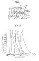
- the light emission layer 14 is formed of a plurality of layers each containing one kind of fluorescent substance. As shown in Fig. 1 , the light emission layer 14 includes a blue region emission layer 14a having a peak wavelength in a blue region ranging from 445 nm to 455 nm and a red region emission layer 14b having a peak wavelength in a red region of 600 nm or more. The light emission layer 14 further includes a green region emission layer. The light emission layer is configured to emit a white light through the use of the blue region emission layer 14a, the red region emission layer 14b and the green region emission layer 14c.
- the blue region emission layer 14a is made of, e.g., TBP (tributyl phosphate) designated by "LA” in Fig. 2 which shows a spectral distribution or sty-NPD designated by "LB” in Fig. 2 .
- TBP tributyl phosphate
- LA tributyl phosphate
- LB sty-NPD
- the material of the blue region emission layer 14a may be appropriately changed to other fluorescent substances having a peak wavelength in a blue wavelength region ranging from 445 nm to 455 nm.
- the red region emission layer 14b is made of, e.g., PQ 2 Ir (acac), a red phosphorous complex, designated by "LE” in Fig. 2 .
- the material of the red region emission layer 14b may be appropriately changed to other fluorescent substances having a peak wavelength in a red wavelength region of 600 nm or more.
- the green region emission layer 14c is made of, e.g., Ir(ppy) 3 , a green iridium complex, designated by "LC” in Fig. 2 or C545T (10-1,3-benzothiazol-2-yl)-1,1,7,7-tetramethyl-2,3,6,7-tetrahydro-1H,5H,11H-pyrano[2,3-f]pyrido[3,2,1-ij]quinoline-11-one) designated by "LD” in Fig. 2 .
- the electron transport layer 15 is made of an electron-transporting material, e.g., a compound which is capable of transporting electrons, has an effect of receiving electrons from the cathode electrode 16, has a superior effect of injecting electrons into the light emission layer 14 or a light emitting material, prevents movement of holes toward the electron transport layer 15 and has a superior thin film forming capability.
- an electron-transporting material e.g., a compound which is capable of transporting electrons
- examples of the electron-transporting material include fluorene, bathophenanthroline, bathocuproine, anthraquinodimethane, diphenoquinone, oxazole, oxadiazole, triazole, imidazole, anthraquinodimethane, compounds thereof, metal complex compounds thereof and nitrogen-containing pentacyclic derivatives thereof.
- metal complex compounds include, but are not limited to, tris(8-hydroxy quinolinate)aluminum, tri(2-methyl-8-hydroxy quinolinate)aluminum, tris(8-hydroxy quinolinate)gallium, bis(10-hydroxy benzo[h]quinolinate)beryllium, bis(10-hydroxy benzo[h]quinolinate)zinc, bis(2-methyl-8-quinolinate)(o-crezolate)gallium, bis(2-methyl-8-quinolinate)(1-naphtholate)aluminum and the like.
- nitrogen-containing pentacyclic derivatives it is preferable to use oxazole, thiazole, oxadiazole, thiadiazole or triazole derivatives. More specifically, examples of the nitrogen-containing pentacyclic derivatives include, but are not limited to, 2,5-bis(1-phenyl)-1,3,4-oxazole, 2,5-bis(1-phenyl)-1,3,4-thiazole, 2,5-bis(1-phenyl)1,3,4-oxadiazole, 2-(4'-tert-bytylphenyl)-5-(4"-biphenyl)1,3,4-oxadiazole, 2,5-bis(1-naphthyl)-1,3,4-oxadiazole, 1,4-bis[2-(5-phenylthiadiazolyl)]benzene, 2,5-bis(1-naphthyl),1,3,4-triazole, 3-(4-biphenylyl)
- the cathode electrode 16 is an electrode for injecting electrons into the light emission layer 14.
- the cathode electrode 16 is preferably made of an electrode material including a metal, an alloy, an electrically conductive compound and mixtures thereof, all of which have a small work function. More specifically, examples of the electrode material include sodium, a sodium-potassium alloy, lithium, magnesium, aluminum, a magnesium-silver mixture, a magnesium-indium mixture, an aluminum-lithium alloy, an Al/A1 2 0 3 mixture and an Al/LiF mixture.
- the relative spectral intensity of a blue light at an emission peak wavelength of about 445 nm is set equal to 1.
- the relative spectral intensity of the blue light at an emission wavelength of 475 nm is about 0.65.
- the emission peak wavelength of a red light is set equal to about 610 nm and the color temperature of the emitted red light is about 6400K.
- the spectral characteristic of the white organic electroluminescence device 10 thus configured is shown in Fig. 4 .
- the relative spectral intensity of a blue light at an emission peak wavelength of about 455 nm is set equal to 1.
- the relative spectral intensity of the blue light at an emission wavelength of 485 nm is about 0.8.
- the emission peak wavelength of a red light is set equal to about 600 nm, and the color temperature of the emitted red light emitted is about 6400K.
- the spectral characteristic of the white organic electroluminescence device 10 thus configured is shown in Fig. 5 .
- the relative spectral intensity of a blue light at an emission peak wavelength of about 440 nm is set equal to 1.
- the relative spectral intensity of the blue light at an emission wavelength of 470 nm is about 0.7.
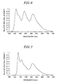
- the emission peak wavelength of a red light is set equal to about 595 nm and the color temperature of the emitted red light is about 6400K.
- the spectral characteristic of the white organic electroluminescence device 10 thus configured is shown in Fig. 6 .
- the relative spectral intensity of a blue light at an emission peak wavelength of about 460 nm is set equal to 1.
- the relative spectral intensity of the blue light at an emission wavelength of 490 nm is about 0.68.
- the emission peak wavelength of a red light is set equal to about 595 nm, and the color temperature of the emitted red light is about 6400K.
- the spectral characteristic of the white organic electroluminescence device 10 thus configured is shown in Fig. 7 .
- the skin color favorability index of Japanese women PS disclosed in, e.g., Japanese Patent Application Publication 1999-258047 can be increased to 90.
- This value is sufficiently higher than the PS of comparative example 1 which is 66 and the PS of comparative example 2 which is 84.
- the average color rendering index Ra can be increased to 90. It is possible to obtain a high enough color rendering property as compared with comparative example 2 of which Ra is 73.
- the average color rendering index Ra can be increased to 80 or more which value is recommended by JIS Z 9110 "General Provisions on Lighting Standards" as the average color rendering index in a house or an office work space.
- the skin color favorability index of Japanese women PS can be increased to 96. This value is higher than the PS of comparative example 1 which is 66 and the PS of comparative example 2 which is 84.
- the average color rendering index Ra can be increased to 82. It is possible to obtain a high enough color rendering property as compared with comparative example 2 of which Ra is 73.
- the average color rendering index Ra can be increased to 80 or more which value is recommended by JIS Z 9110 "General Provisions on Lighting Standards" as the average color rendering index in a house or an office work space.
- the white organic electroluminescence device 10 configured as above, when a positive voltage is applied to the anode electrode 12 and a negative voltage is applied to the cathode electrode 16, the holes and the electrons injected into the light emission layer 14 through the hole transport layer 13 and the electron transport layer 15 are recombined, e.g., in the light emission layer 14 and at the interface between the light emission layer 14 and the hole transport layer 13, thereby generating light emission.
- the light emission layer 14 is formed of a plurality of layers (blue, red and green region light emission layers 14a to 14c) laminated one above another. The lights of different colors emitted from the respective layers 14a to 14c are mixed with each other, whereby the device 10 can emit a white light.
- the white organic electroluminescence device 10 is configured such that the blue region emission layer 14a has a peak wavelength ranging from 445 nm to 455 nm. This makes it possible to increase the average color rendering index Ra to 80 or more and to increase the skin color favorability index of Japanese women PS to 90 or more.
- the device 10 is configured such that the red region emission layer 14b has a peak wavelength of 600 nm or more. This enables the light emitted from the light emission layer 14 to have a longer wavelength, which assists in increasing the skin color favorability index of Japanese women PS.
- the embodiment of the present invention may be modified as follows. While the light emission layer 14 is formed of three layers, namely the blue region emission layer 14a, the red region emission layer 14b and the green region emission layer 14c in the embodiment described above, the number of layers may be arbitrarily changed as long as the light emitted from the respective layers have peak wavelengths (emission peaks) in the blue, red and green wavelength regions.
- the white organic electroluminescence device 10 may be used as a variety of lighting devices such as a base light, a down-light, a spotlight, a bracket light, a pendant light and a sealing light.
Landscapes
- Engineering & Computer Science (AREA)
- Manufacturing & Machinery (AREA)
- Chemical & Material Sciences (AREA)
- Physics & Mathematics (AREA)
- Optics & Photonics (AREA)
- Materials Engineering (AREA)
- Organic Chemistry (AREA)
- Electroluminescent Light Sources (AREA)
Abstract
Description
- The present invention relates to a white organic electroluminescence device.
- A white organic electroluminescence device disclosed in, e.g., Japanese Patent Application Publication No.
2004-63349 JP2004-63349A - In the white organic electroluminescence device of
JP2004-63349A - In the conventional white organic electroluminescence device, however, the color rendering index Ra becomes lower if the peak wavelength of a blue light is set to lie in a longer wavelength region in order to increase the skin color favorability index of Japanese women PS.
- In view of the above, the present invention provides a white organic electroluminescence device capable of increasing a skin color favorability index of Japanese women PS while preventing a decrease in color rendering property.
- In accordance with an aspect of the present invention, there is provided a white organic electroluminescence device including: an anode electrode; a cathode electrode; a hole transport layer arranged between the anode electrode and the cathode electrode; an electron transport layer arranged between the anode electrode and the cathode electrode; and a plurality of light emission layers into which holes and electrons are injected from the hole transport layer and the electron transport layer, the light emission layers arranged between the hole transport layer and the electron transport layer.
- The light emission layers are configured to have at least one emission peak wavelength for each of blue, green and red colors, and the emission peak wavelength of the blue color ranges from about 445 nm to about 455 nm.
- The light emission layers may be configured such that the emission peak wavelength of the red color is about 600 nm or more.
- With the present invention, it is possible to provide a white organic electroluminescence device capable of increasing a skin color favorability index of Japanese women PS while preventing a decrease in color rendering property.
- The objects and features of the present invention will become apparent from the following description of embodiments, given in conjunction with the accompanying drawings, in which:
-
Fig. 1 is a schematic section view for explaining a layer structure of a white organic electroluminescence device in accordance with an embodiment of the present invention; -
Fig. 2 is a spectral characteristic diagram for explaining one example of a light emitting material making up the white organic electroluminescence device; -
Fig. 3 is an explanatory view for explaining differences in effectiveness between conditions A and B and comparative examples 1 and 2; -
Fig. 4 is a spectral characteristic diagram of the white organic electroluminescence device under condition A; -
Fig. 5 is a spectral characteristic diagram of the white organic electroluminescence device under condition B; -
Fig. 6 is a spectral characteristic diagram of a white organic electroluminescence device according to comparative example 1; and -
Fig. 7 is a spectral characteristic diagram of a white organic electroluminescence device according to comparative example 2. - Embodiments of the present invention will now be described with reference to the accompanying drawings which form a part hereof.
- Referring to
Fig. 1 , the whiteorganic electroluminescence device 10 of the present embodiment includes asubstrate 11 formed of a transparent glass panel or the like. Ananode electrode 12 formed of a transparent conductive film or the like is laminated on thesubstrate 11. Alight emission layer 14 is laminated on theanode electrode 12 through ahole transport layer 13. Acathode electrode 16 is laminated on thelight emission layer 14 through anelectron transport layer 15. - The
anode electrode 12 is an electrode for injecting holes into the device and is made, e.g., of a metal such as gold or the like or a conductive transparent material such as CuI, ITO, SnO2, ZnO, IZO or the like. - The
hole transport layer 13 is made of a hole-transporting material, e.g., a compound which is capable of transporting holes, has an effect of receiving holes from theanode electrode 12, has a superior effect of injecting holes into thelight emission layer 14, prevents movement of electrons toward thehole transport layer 13 and has a superior thin film forming capability. - More specifically, examples of the hole-transporting material include, but are not limited to, polymer materials including a phthalocyanine derivative, a naphthalocyanine derivative, a porphyrin derivative, an aromatic diamine compound such as a N, N'-bis(3-methylphenyl)-(1,1'-biphenyl)-4,4'-diamine (TPD) or a 4,4'-bis[N-(naphthyl)-N-phenyl-amino]biphenyl (α-NPD), an oxazole, an oxadiazole, a triazole, an imidazole, an imidazolone, a stilbene derivative, a pyrazoline derivative, a tetrahydroimidazole, a polyarylalkane, a butadiene, a 4,4',4"-tris(N-(3-methylphenyl)N-phenyl-amino)triphenylamine (m-MTDATA), an electrically-conductive polymer such as a polyvinylcarbazole, a polysilane or a polyethylenedioxy thiophene (PEDOT) and the like.
- The
light emission layer 14 is formed of a plurality of layers each containing one kind of fluorescent substance. As shown inFig. 1 , thelight emission layer 14 includes a blueregion emission layer 14a having a peak wavelength in a blue region ranging from 445 nm to 455 nm and a redregion emission layer 14b having a peak wavelength in a red region of 600 nm or more. Thelight emission layer 14 further includes a green region emission layer. The light emission layer is configured to emit a white light through the use of the blueregion emission layer 14a, the redregion emission layer 14b and the greenregion emission layer 14c. - The blue
region emission layer 14a is made of, e.g., TBP (tributyl phosphate) designated by "LA" inFig. 2 which shows a spectral distribution or sty-NPD designated by "LB" inFig. 2 . The material of the blueregion emission layer 14a may be appropriately changed to other fluorescent substances having a peak wavelength in a blue wavelength region ranging from 445 nm to 455 nm. - The red
region emission layer 14b is made of, e.g., PQ2Ir (acac), a red phosphorous complex, designated by "LE" inFig. 2 . The material of the redregion emission layer 14b may be appropriately changed to other fluorescent substances having a peak wavelength in a red wavelength region of 600 nm or more. - The green
region emission layer 14c is made of, e.g., Ir(ppy)3, a green iridium complex, designated by "LC" inFig. 2 or C545T (10-1,3-benzothiazol-2-yl)-1,1,7,7-tetramethyl-2,3,6,7-tetrahydro-1H,5H,11H-pyrano[2,3-f]pyrido[3,2,1-ij]quinoline-11-one) designated by "LD" inFig. 2 . - The
electron transport layer 15 is made of an electron-transporting material, e.g., a compound which is capable of transporting electrons, has an effect of receiving electrons from thecathode electrode 16, has a superior effect of injecting electrons into thelight emission layer 14 or a light emitting material, prevents movement of holes toward theelectron transport layer 15 and has a superior thin film forming capability. - More specifically, examples of the electron-transporting material include fluorene, bathophenanthroline, bathocuproine, anthraquinodimethane, diphenoquinone, oxazole, oxadiazole, triazole, imidazole, anthraquinodimethane, compounds thereof, metal complex compounds thereof and nitrogen-containing pentacyclic derivatives thereof. Examples of the metal complex compounds include, but are not limited to, tris(8-hydroxy quinolinate)aluminum, tri(2-methyl-8-hydroxy quinolinate)aluminum, tris(8-hydroxy quinolinate)gallium, bis(10-hydroxy benzo[h]quinolinate)beryllium, bis(10-hydroxy benzo[h]quinolinate)zinc, bis(2-methyl-8-quinolinate)(o-crezolate)gallium, bis(2-methyl-8-quinolinate)(1-naphtholate)aluminum and the like.
- As the nitrogen-containing pentacyclic derivatives, it is preferable to use oxazole, thiazole, oxadiazole, thiadiazole or triazole derivatives. More specifically, examples of the nitrogen-containing pentacyclic derivatives include, but are not limited to, 2,5-bis(1-phenyl)-1,3,4-oxazole, 2,5-bis(1-phenyl)-1,3,4-thiazole, 2,5-bis(1-phenyl)1,3,4-oxadiazole, 2-(4'-tert-bytylphenyl)-5-(4"-biphenyl)1,3,4-oxadiazole, 2,5-bis(1-naphthyl)-1,3,4-oxadiazole, 1,4-bis[2-(5-phenylthiadiazolyl)]benzene, 2,5-bis(1-naphthyl),1,3,4-triazole, 3-(4-biphenylyl)-4-phenyl-5-(4-t-butyphenyl)-1,2,4-triazole and the like. Moreover, it is possible to use polymer materials for use in manufacturing a polymer-based organic electroluminescence device. Examples of the polymer materials include polyparaphenylene, derivatives thereof, fluorene, derivatives thereof and the like.
- The
cathode electrode 16 is an electrode for injecting electrons into thelight emission layer 14. Thecathode electrode 16 is preferably made of an electrode material including a metal, an alloy, an electrically conductive compound and mixtures thereof, all of which have a small work function. More specifically, examples of the electrode material include sodium, a sodium-potassium alloy, lithium, magnesium, aluminum, a magnesium-silver mixture, a magnesium-indium mixture, an aluminum-lithium alloy, an Al/A1 203 mixture and an Al/LiF mixture. - Next, differences in effectiveness between individual conditions in the white
organic electroluminescence device 10 of the present embodiment will be described with reference toFigs. 3 through 7 . The effectiveness is evaluated with respect to conditions A and B and comparative examples 1 and 2 by referring toFig. 3 . - The relative spectral intensity of a blue light at an emission peak wavelength of about 445 nm is set equal to 1. In this case, the relative spectral intensity of the blue light at an emission wavelength of 475 nm is about 0.65. The emission peak wavelength of a red light is set equal to about 610 nm and the color temperature of the emitted red light is about 6400K. The spectral characteristic of the white
organic electroluminescence device 10 thus configured is shown inFig. 4 . - The relative spectral intensity of a blue light at an emission peak wavelength of about 455 nm is set equal to 1. In this case, the relative spectral intensity of the blue light at an emission wavelength of 485 nm is about 0.8. The emission peak wavelength of a red light is set equal to about 600 nm, and the color temperature of the emitted red light emitted is about 6400K. The spectral characteristic of the white
organic electroluminescence device 10 thus configured is shown inFig. 5 . - The relative spectral intensity of a blue light at an emission peak wavelength of about 440 nm is set equal to 1. In this case, the relative spectral intensity of the blue light at an emission wavelength of 470 nm is about 0.7. The emission peak wavelength of a red light is set equal to about 595 nm and the color temperature of the emitted red light is about 6400K. The spectral characteristic of the white
organic electroluminescence device 10 thus configured is shown inFig. 6 . - The relative spectral intensity of a blue light at an emission peak wavelength of about 460 nm is set equal to 1. In this case, the relative spectral intensity of the blue light at an emission wavelength of 490 nm is about 0.68. The emission peak wavelength of a red light is set equal to about 595 nm, and the color temperature of the emitted red light is about 6400K. The spectral characteristic of the white
organic electroluminescence device 10 thus configured is shown inFig. 7 . - If the respective
light emission layers 1999-258047 light emission layers - If the respective
light emission layers light emission layers - Next, description will be made on the operation of the present embodiment.
- In the white
organic electroluminescence device 10 configured as above, when a positive voltage is applied to theanode electrode 12 and a negative voltage is applied to thecathode electrode 16, the holes and the electrons injected into thelight emission layer 14 through thehole transport layer 13 and theelectron transport layer 15 are recombined, e.g., in thelight emission layer 14 and at the interface between thelight emission layer 14 and thehole transport layer 13, thereby generating light emission. In this regard, thelight emission layer 14 is formed of a plurality of layers (blue, red and green regionlight emission layers 14a to 14c) laminated one above another. The lights of different colors emitted from therespective layers 14a to 14c are mixed with each other, whereby thedevice 10 can emit a white light. - Pursuant to the comparison results stated above, the white
organic electroluminescence device 10 is configured such that the blueregion emission layer 14a has a peak wavelength ranging from 445 nm to 455 nm. This makes it possible to increase the average color rendering index Ra to 80 or more and to increase the skin color favorability index of Japanese women PS to 90 or more. In addition, thedevice 10 is configured such that the redregion emission layer 14b has a peak wavelength of 600 nm or more. This enables the light emitted from thelight emission layer 14 to have a longer wavelength, which assists in increasing the skin color favorability index of Japanese women PS. - Next, description will be made on the distinctive effects provided by the present embodiment.
- (1) The
light emission layers region emission layer 14a in the blue region exists in a wavelength region between 445 nm and 455 nm. This makes it possible to increase the average color rendering index Ra to 80 or more and to increase the skin color favorability index of Japanese women PS to 90 or more. It is therefore possible to increase the PS value indicating the skin color favorability index, while preventing a decrease in the color rendering property. - (2) The
light emission layers region emission layer 14b exists in a wavelength region of 600 nm or more. This enables the light emitted from thelight emission layer 14 to have a longer wavelength, which assists in increasing the skin color favorability index of Japanese women PS. - The embodiment of the present invention may be modified as follows. While the
light emission layer 14 is formed of three layers, namely the blueregion emission layer 14a, the redregion emission layer 14b and the greenregion emission layer 14c in the embodiment described above, the number of layers may be arbitrarily changed as long as the light emitted from the respective layers have peak wavelengths (emission peaks) in the blue, red and green wavelength regions. - While not specifically mentioned in the foregoing embodiment, the white
organic electroluminescence device 10 may be used as a variety of lighting devices such as a base light, a down-light, a spotlight, a bracket light, a pendant light and a sealing light. - While the invention has been shown and described with respect to the embodiments, the present invention is not limited thereto. It will be understood by those skilled in the art that various changes and modifications may be made without departing from the scope of the invention as defined in the following claims.
Claims (2)
- A white organic electroluminescence device, comprising:an anode electrode;a cathode electrode;a hole transport layer arranged between the anode electrode and the cathode electrode;an electron transport layer arranged between the anode electrode and the cathode electrode; anda plurality of light emission layers into which holes and electrons are injected from the hole transport layer and the electron transport layer, the light emission layers arranged between the hole transport layer and the electron transport layer,wherein the light emission layers are configured to have at least one emission peak wavelength for each of blue, green and red colors, and the emission peak wavelength of the blue color ranges from about 445 nm to about 455 nm.
- The device of claim 1, wherein the light emission layers are configured such that the emission peak wavelength of the red color is about 600 nm or more.
Applications Claiming Priority (1)
| Application Number | Priority Date | Filing Date | Title |
|---|---|---|---|
| JP2011094843A JP2012227042A (en) | 2011-04-21 | 2011-04-21 | White organic electroluminescent element |
Publications (1)
| Publication Number | Publication Date |
|---|---|
| EP2515616A1 true EP2515616A1 (en) | 2012-10-24 |
Family
ID=46049143
Family Applications (1)
| Application Number | Title | Priority Date | Filing Date |
|---|---|---|---|
| EP12002699A Withdrawn EP2515616A1 (en) | 2011-04-21 | 2012-04-18 | White organic electroluminescence device |
Country Status (4)
| Country | Link |
|---|---|
| US (1) | US8866163B2 (en) |
| EP (1) | EP2515616A1 (en) |
| JP (1) | JP2012227042A (en) |
| CN (1) | CN102751441B (en) |
Cited By (1)
| Publication number | Priority date | Publication date | Assignee | Title |
|---|---|---|---|---|
| US10854682B2 (en) | 2014-08-08 | 2020-12-01 | Semiconductor Energy Laboratory Co., Ltd. | Light-emitting device, electronic device, and lighting device |
Citations (5)
| Publication number | Priority date | Publication date | Assignee | Title |
|---|---|---|---|---|
| JPH11258047A (en) | 1998-03-13 | 1999-09-24 | Matsushita Electric Ind Co Ltd | Method for evaluating color rendering properties of lighting lamps |
| EP1286569A1 (en) * | 2001-08-15 | 2003-02-26 | Eastman Kodak Company | White organic light-emitting devices with improved efficiency |
| JP2004063349A (en) | 2002-07-30 | 2004-02-26 | Matsushita Electric Works Ltd | White organic electroluminescent element and design method of white organic electroluminescent element |
| US20040058193A1 (en) * | 2002-09-16 | 2004-03-25 | Eastman Kodak Company | White organic light-emitting devices with improved performance |
| US20050056969A1 (en) * | 2003-09-16 | 2005-03-17 | Eastman Kodak Company | Forming homogeneous mixtures of organic materials for physical vapor deposition using a solvent |
Family Cites Families (9)
| Publication number | Priority date | Publication date | Assignee | Title |
|---|---|---|---|---|
| JPS61203591A (en) | 1985-03-05 | 1986-09-09 | 松下電器産業株式会社 | Manufacture of thin film el element |
| JPH103990A (en) | 1996-06-13 | 1998-01-06 | Idemitsu Kosan Co Ltd | Organic EL light emitting device |
| US5851063A (en) | 1996-10-28 | 1998-12-22 | General Electric Company | Light-emitting diode white light source |
| US6577073B2 (en) * | 2000-05-31 | 2003-06-10 | Matsushita Electric Industrial Co., Ltd. | Led lamp |
| US7023013B2 (en) * | 2004-06-16 | 2006-04-04 | Eastman Kodak Company | Array of light-emitting OLED microcavity pixels |
| JP2006024648A (en) * | 2004-07-06 | 2006-01-26 | Toyota Industries Corp | Lighting device |
| US8040045B2 (en) | 2005-07-14 | 2011-10-18 | Koninklijke Philips Electronics N.V. | Electroluminescent light source |
| JP5415664B2 (en) | 2005-12-22 | 2014-02-12 | パナソニック株式会社 | Light source device |
| JP5102666B2 (en) | 2008-03-18 | 2012-12-19 | パナソニック株式会社 | ORGANIC ELECTROLUMINESCENT ELEMENT AND LIGHTING DEVICE |
-
2011
- 2011-04-21 JP JP2011094843A patent/JP2012227042A/en not_active Withdrawn
-
2012
- 2012-04-18 EP EP12002699A patent/EP2515616A1/en not_active Withdrawn
- 2012-04-19 CN CN201210116290.7A patent/CN102751441B/en not_active Expired - Fee Related
- 2012-04-20 US US13/451,803 patent/US8866163B2/en not_active Expired - Fee Related
Patent Citations (5)
| Publication number | Priority date | Publication date | Assignee | Title |
|---|---|---|---|---|
| JPH11258047A (en) | 1998-03-13 | 1999-09-24 | Matsushita Electric Ind Co Ltd | Method for evaluating color rendering properties of lighting lamps |
| EP1286569A1 (en) * | 2001-08-15 | 2003-02-26 | Eastman Kodak Company | White organic light-emitting devices with improved efficiency |
| JP2004063349A (en) | 2002-07-30 | 2004-02-26 | Matsushita Electric Works Ltd | White organic electroluminescent element and design method of white organic electroluminescent element |
| US20040058193A1 (en) * | 2002-09-16 | 2004-03-25 | Eastman Kodak Company | White organic light-emitting devices with improved performance |
| US20050056969A1 (en) * | 2003-09-16 | 2005-03-17 | Eastman Kodak Company | Forming homogeneous mixtures of organic materials for physical vapor deposition using a solvent |
Non-Patent Citations (4)
| Title |
|---|
| CHENG GANG ET AL: "White organic light-emitting devices with a phosphorescent multiple emissive layer", APPLIED PHYSICS LETTERS, AIP, AMERICAN INSTITUTE OF PHYSICS, MELVILLE, NY, US, vol. 89, no. 4, 25 July 2006 (2006-07-25), pages 43504 - 043504, XP012088186, ISSN: 0003-6951, DOI: 10.1063/1.2227645 * |
| HAQ K U ET AL: "Red organic light-emitting diodes with high efficiency, low driving voltage and saturated red color realized via two step energy transfer based on ADN and Alq3 co-host system", CURRENT APPLIED PHYSICS, NORTH-HOLLAND, AMSTERDAM, NL, vol. 9, no. 1, 1 January 2009 (2009-01-01), pages 257 - 262, XP025408596, ISSN: 1567-1739, [retrieved on 20080220], DOI: 10.1016/J.CAP.2008.02.005 * |
| JARIKOV VIKTOR: "Improving operating lifetime of organic light-emitting diodes with polycyclic aromatic hydrocarbons as aggregating light-emitting-layer additives", JOURNAL OF APPLIED PHYSICS, AMERICAN INSTITUTE OF PHYSICS. NEW YORK, US, vol. 100, no. 1, 5 July 2006 (2006-07-05), pages 14901 - 014901, XP012088916, ISSN: 0021-8979, DOI: 10.1063/1.2214535 * |
| YINGFANG ZHANG ET AL: "Blue and white organic light-emitting devices using oligo(phenylenvinylene) as a blue emitter", SEMICONDUCTOR SCIENCE AND TECHNOLOGY, IOP PUBLISHING LTD, GB, vol. 22, no. 3, 1 March 2007 (2007-03-01), pages 214 - 217, XP020114945, ISSN: 0268-1242, DOI: 10.1088/0268-1242/22/3/007 * |
Cited By (2)
| Publication number | Priority date | Publication date | Assignee | Title |
|---|---|---|---|---|
| US10854682B2 (en) | 2014-08-08 | 2020-12-01 | Semiconductor Energy Laboratory Co., Ltd. | Light-emitting device, electronic device, and lighting device |
| US11917882B2 (en) | 2014-08-08 | 2024-02-27 | Semiconductor Energy Laboratory Co., Ltd. | Light-emitting device, electronic device, and lighting device |
Also Published As
| Publication number | Publication date |
|---|---|
| JP2012227042A (en) | 2012-11-15 |
| CN102751441A (en) | 2012-10-24 |
| US8866163B2 (en) | 2014-10-21 |
| CN102751441B (en) | 2015-12-09 |
| US20120267652A1 (en) | 2012-10-25 |
Similar Documents
| Publication | Publication Date | Title |
|---|---|---|
| JP5699282B2 (en) | Organic electroluminescence device and lighting apparatus | |
| KR101453874B1 (en) | White organic light emitting device | |
| JP4886352B2 (en) | Organic electroluminescence device | |
| JP5685734B2 (en) | Organic electroluminescence element, lighting apparatus, and food storage | |
| WO2014068970A1 (en) | Organic electroluminescence element and illumination device | |
| JP2009224274A (en) | Organic electroluminescent element, and lighting device | |
| CN103477714A (en) | Organic electroluminescent element | |
| JP2012204096A (en) | Organic electroluminescent element | |
| JP4230732B2 (en) | Design method of white organic electroluminescent device | |
| EP2874471A1 (en) | Organic electroluminescent element | |
| JP4432299B2 (en) | Planar light emitter | |
| JP3967946B2 (en) | Organic electroluminescence device | |
| JP2003282265A (en) | Organic electroluminescent device | |
| US8866163B2 (en) | White organic electroluminescence device | |
| JP5167380B2 (en) | Organic electroluminescence device | |
| KR100760901B1 (en) | The White Organic Light Emitting Device | |
| JP2008218320A (en) | Organic electroluminescent element | |
| JP5180338B2 (en) | Organic electroluminescence device | |
| JP2003282267A (en) | Light emitting element | |
| JP5544040B2 (en) | Organic electroluminescence device | |
| JP6078701B1 (en) | White light emitting organic EL panel and manufacturing method thereof | |
| JP5870304B2 (en) | Organic electroluminescence device | |
| JP5879526B2 (en) | Organic electroluminescence device | |
| JP2013069702A (en) | Organic electroluminescent element | |
| JP2013084986A (en) | Organic electroluminescent element |
Legal Events
| Date | Code | Title | Description |
|---|---|---|---|
| PUAI | Public reference made under article 153(3) epc to a published international application that has entered the european phase |
Free format text: ORIGINAL CODE: 0009012 |
|
| AK | Designated contracting states |
Kind code of ref document: A1 Designated state(s): AL AT BE BG CH CY CZ DE DK EE ES FI FR GB GR HR HU IE IS IT LI LT LU LV MC MK MT NL NO PL PT RO RS SE SI SK SM TR |
|
| AX | Request for extension of the european patent |
Extension state: BA ME |
|
| 17P | Request for examination filed |
Effective date: 20130424 |
|
| 17Q | First examination report despatched |
Effective date: 20140228 |
|
| RAP1 | Party data changed (applicant data changed or rights of an application transferred) |
Owner name: PANASONIC INTELLECTUAL PROPERTY MANAGEMENT CO., LT |
|
| STAA | Information on the status of an ep patent application or granted ep patent |
Free format text: STATUS: THE APPLICATION IS DEEMED TO BE WITHDRAWN |
|
| 18D | Application deemed to be withdrawn |
Effective date: 20150505 |