EP2514120B1 - Apparatus and method for receiving a polarisation-multiplexed optical signal - Google Patents
Apparatus and method for receiving a polarisation-multiplexed optical signal Download PDFInfo
- Publication number
- EP2514120B1 EP2514120B1 EP10793224.6A EP10793224A EP2514120B1 EP 2514120 B1 EP2514120 B1 EP 2514120B1 EP 10793224 A EP10793224 A EP 10793224A EP 2514120 B1 EP2514120 B1 EP 2514120B1
- Authority
- EP
- European Patent Office
- Prior art keywords
- polarization
- optical
- receiving
- dependent
- diverse
- Prior art date
- Legal status (The legal status is an assumption and is not a legal conclusion. Google has not performed a legal analysis and makes no representation as to the accuracy of the status listed.)
- Active
Links
Images

Classifications
-
- H—ELECTRICITY
- H04—ELECTRIC COMMUNICATION TECHNIQUE
- H04B—TRANSMISSION
- H04B10/00—Transmission systems employing electromagnetic waves other than radio-waves, e.g. infrared, visible or ultraviolet light, or employing corpuscular radiation, e.g. quantum communication
- H04B10/60—Receivers
- H04B10/66—Non-coherent receivers, e.g. using direct detection
- H04B10/67—Optical arrangements in the receiver
- H04B10/671—Optical arrangements in the receiver for controlling the input optical signal
-
- H—ELECTRICITY
- H04—ELECTRIC COMMUNICATION TECHNIQUE
- H04B—TRANSMISSION
- H04B10/00—Transmission systems employing electromagnetic waves other than radio-waves, e.g. infrared, visible or ultraviolet light, or employing corpuscular radiation, e.g. quantum communication
- H04B10/25—Arrangements specific to fibre transmission
- H04B10/2507—Arrangements specific to fibre transmission for the reduction or elimination of distortion or dispersion
- H04B10/2572—Arrangements specific to fibre transmission for the reduction or elimination of distortion or dispersion due to forms of polarisation-dependent distortion other than PMD
-
- H—ELECTRICITY
- H04—ELECTRIC COMMUNICATION TECHNIQUE
- H04B—TRANSMISSION
- H04B10/00—Transmission systems employing electromagnetic waves other than radio-waves, e.g. infrared, visible or ultraviolet light, or employing corpuscular radiation, e.g. quantum communication
- H04B10/60—Receivers
- H04B10/61—Coherent receivers
-
- H—ELECTRICITY
- H04—ELECTRIC COMMUNICATION TECHNIQUE
- H04B—TRANSMISSION
- H04B10/00—Transmission systems employing electromagnetic waves other than radio-waves, e.g. infrared, visible or ultraviolet light, or employing corpuscular radiation, e.g. quantum communication
- H04B10/60—Receivers
- H04B10/61—Coherent receivers
- H04B10/614—Coherent receivers comprising one or more polarization beam splitters, e.g. polarization multiplexed [PolMux] X-PSK coherent receivers, polarization diversity heterodyne coherent receivers
-
- H—ELECTRICITY
- H04—ELECTRIC COMMUNICATION TECHNIQUE
- H04B—TRANSMISSION
- H04B10/00—Transmission systems employing electromagnetic waves other than radio-waves, e.g. infrared, visible or ultraviolet light, or employing corpuscular radiation, e.g. quantum communication
- H04B10/60—Receivers
- H04B10/61—Coherent receivers
- H04B10/616—Details of the electronic signal processing in coherent optical receivers
- H04B10/6162—Compensation of polarization related effects, e.g., PMD, PDL
-
- H—ELECTRICITY
- H04—ELECTRIC COMMUNICATION TECHNIQUE
- H04B—TRANSMISSION
- H04B10/00—Transmission systems employing electromagnetic waves other than radio-waves, e.g. infrared, visible or ultraviolet light, or employing corpuscular radiation, e.g. quantum communication
- H04B10/60—Receivers
- H04B10/66—Non-coherent receivers, e.g. using direct detection
- H04B10/69—Electrical arrangements in the receiver
-
- H—ELECTRICITY
- H04—ELECTRIC COMMUNICATION TECHNIQUE
- H04J—MULTIPLEX COMMUNICATION
- H04J14/00—Optical multiplex systems
- H04J14/06—Polarisation multiplex systems
Definitions
- the present invention refers to optical receivers and methods for receiving optical signals, and in particular to improved methods and apparatus for reducing system deteriorations due to polarization effects.
- a polarization diverse coherent detector is often combined with a polarization multiplexed (POLMUX) signal.
- POLMUX polarization multiplexed
- a POLMUX signal carries information on the two states of polarization that single-mode fiber supports and allows to double the spectral efficiency of a transmission system.
- polarization multiplexed signals are affected by polarization dependant loss (PDL) resulting in signal degradation and higher bit error rate (BER) which limits maximum transmission distance.
- PDL polarization dependant loss
- BER bit error rate
- SOAs Semiconductor Optical Amplifiers
- PDG polarization dependent gain
- an improved optical receiving apparatus for receiving a polarization multiplexed optical signal and an improved method for receiving an optical signal.
- the improved optical receiving apparatus and method for receiving an optical signal should be capable of significantly reducing the influence of polarization dependent gain (PDG) and polarization dependant loss (PDL) therefore improving the signal's performance.
- PDG polarization dependent gain
- PDL polarization dependant loss
- an optical receiving apparatus for receiving a polarization multiplexed optical signal, comprising a polarization dependent element receiving the polarization multiplexed optical signal, wherein said polarization dependent element has principal axes of polarization;
- the polarization maintaining optical element may be a polarization maintaining optical fiber.
- the polarization dependent element may be a polarization dependent gain element.
- the polarization dependent element may be a polarization dependent loss element.
- the polarization dependent gain element may be a semiconductor optical amplifier.
- the polarization dependent gain element is an erbium doped optical amplifier.
- a method for receiving an optical signal comprising the steps of receiving the polarization multiplexed optical signal by a polarisation depending element having principal axes of polarization;
- the polarisation depending element is a semiconductor optical amplifier
- the polarization maintaining optical element (3) is a polarization maintaining fiber
- the polarization diverse receiving element is a coherent polarization depending receiving element.
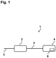
- FIG 1 is a high level block diagram which illustrates an optical receiving apparatus 1 for receiving an optical signal 5, which may be a polarization multiplexed optical signal, according to one embodiment of the invention.
- the optical receiving apparatus 1 includes a polarization diverse optical receiving element 4, which may be a polarization diverse optical receiver, a polarization maintaining optical element 3, (for example a polarization maintaining optical fiber) directly coupled with the polarization diverse optical receiving element 4 and a polarization dependent element 2 directly coupled with the polarization maintaining optical element 3.
- a polarization diverse optical receiving element 4 which may be a polarization diverse optical receiver
- a polarization maintaining optical element 3 for example a polarization maintaining optical fiber
- the polarization maintaining optical element 3 is directly connected to the polarization diverse optical receiving element 4 at one end, and to the polarization dependent element 2 at the other end.
- the polarization maintaining optical fiber is meant a birefringent fiber having two principal axes of polarization, also known as the fast and the slow axis, and which supports two well defined orthogonal propagation modes of light whose refractive indices differ by 10 -6 or more.
- the coordinate system of the polarization maintaining optical element 3 is aligned to the coordinate system of the polarization diverse optical receiving element 4, and to the coordinate system of the polarization dependent element 2, so that both coordinate systems coincide with each other.
- the polarization dependent element 2 is a polarization dependent gain element and in particular a semiconductor optical amplifier, like for example an erbium doped optical amplifier or a semiconductor optical amplifier (SOA).
- a semiconductor optical amplifier like for example an erbium doped optical amplifier or a semiconductor optical amplifier (SOA).
- the polarization dependent element 2 is a polarization dependent loss element.
- the alignment of the polarization maintaining optical element 3 fixes the transformation of the polarization dependent gain (PDG) vector or polarization dependent loss (PDL) vector to the coordinate system of the coherent optical receiving element 4 so that both coordinate systems coincide with each other.
- PDG polarization dependent gain
- PDL polarization dependent loss
- the polarization diverse optical receiving element 4 includes an electrical amplifier 6 or a plurality of electrical amplifiers 6 and a plurality of analog-to-digital converters (ADCs).
- ADCs analog-to-digital converters
- the polarization diverse optical receiving element 4 which may be a polarization dependent gain element or a polarization dependent loss element gain element, it is possible to calibrate out the polarization dependent gain (PDG) or polarization dependent loss (PDL) induced by the polarization dependent element 2 utilizing the electrical amplifiers 6 that may be used at the polarization diverse optical receiving element 4 preferably before the analog-to-digital converters (ADCs).
- PDG polarization dependent gain
- PDL polarization dependent loss
- FIG 2 is an illustration of the coordinate systems of the polarization diverse optical receiving element 4, the polarization dependent element 2 and the polarization maintaining optical element 3 according to an embodiment of the invention.
- the coordinate system of the polarization diverse optical receiving element 4 includes the two principal orthogonal axes, the principal axis 26 and the principal axis 27; the coordinate system of the polarization dependent element 2 includes the two principal orthogonal axes, the principal axis 21 and the principal axis 22; the coordinate system of the polarization maintaining optical element 3 includes the two principal orthogonal axes, the principal axis 211 and the principal axis 212.
- the polarization maintaining optical element 3 fixes the transformation of the polarization dependent element vector 25 to the coordinate system of the polarization diverse optical receiving element 4 so that the coordinate system of the polarization dependent element 2 including the principal axis 21 and 22 coincide with the coordinate system of the polarization diverse optical receiving element 4 including the two principal axis 26 and the principal axis 27.
- a principal axis of polarization 211 or 212 of the polarization maintaining optical element 3 is aligned with a principal axis of polarization 26 or 27 of the polarization diverse optical receiving element 4 and that a principal axis of polarization 211 or 212 of the polarization maintaining optical element 3 is aligned with a principal axis of polarization 21 or 22 of the polarization dependent element 2.
- the effect of polarization dependent gain or polarization dependent loss on the orthogonal components 23 and 24 of the optical signal at the polarization dependent element 2 are substantially reduced and equally distributed over the two orthogonal components 28 and 29 at the polarization diverse optical receiving element 4.
- These effects can be further reduced utilizing the electrical amplifiers 6 that may be used at the polarization diverse optical receiving element 4 preferably before the analog-to-digital converters (ADCs).
- ADCs analog-to-digital converters
Landscapes
- Engineering & Computer Science (AREA)
- Computer Networks & Wireless Communication (AREA)
- Signal Processing (AREA)
- Physics & Mathematics (AREA)
- Electromagnetism (AREA)
- Lasers (AREA)
- Optical Communication System (AREA)
Description
- The present invention refers to optical receivers and methods for receiving optical signals, and in particular to improved methods and apparatus for reducing system deteriorations due to polarization effects.
- Conventional fiber-optic transmission systems typically use direct detection and operate at 10 Gb/s and 40 Gb/s. However, especially at 40 Gb/s and above these direct detection systems offer a low tolerance to linear impairments such as chromatic dispersion (CD) and polarization mode dispersion (PMD). The tolerance towards these linear impairments can be increased significantly through the use of conventional coherent detection. In combination with digital signal processing, conventional coherent receivers, and in particular conventional polarization diverse coherent detectors, can provide a better tolerance towards chromatic dispersion (CD) and polarization mode dispersion (PMD) and significant benefits with respect to amplified spontaneous emission (ASE) noise.
- In conventional applications, a polarization diverse coherent detector is often combined with a polarization multiplexed (POLMUX) signal. A POLMUX signal carries information on the two states of polarization that single-mode fiber supports and allows to double the spectral efficiency of a transmission system. However, polarization multiplexed signals are affected by polarization dependant loss (PDL) resulting in signal degradation and higher bit error rate (BER) which limits maximum transmission distance.
- In conventional coherent receivers optical amplification is required in order to enhance the data before that the signal can be detected. In most receivers an erbium-doped fiber amplifier (EDFA) is used for this amplification. Semiconductor Optical Amplifiers (SOAs) can be used as an alternative to erbium-doped fiber amplifiers. The Semiconductor Optical Amplifiers (SOAs) although being cost-effective amplifiers with a small form factor, unfortunately exhibit a polarization dependent gain (PDG), resulting in deterioration of system performance.
- Document Heismann et al.: "Automatic polarisation demultiplexer for polarisation-multiplexed transmission systems", ECOC Montreux, Sept. 12 - 16, 1993 ; Regular papers, Zürich, SEV, CH, Vol.2; 12 September 1993, pages 401-404, XP000492247 discloses an polarisation multiplexed transmission system with an polarisation transformer outputting a polmux signal with constant polarisation axes.
- Based upon the above discussions, it is concluded that there is a need in the art, for an improved optical receiving apparatus for receiving a polarization multiplexed optical signal and an improved method for receiving an optical signal. The improved optical receiving apparatus and method for receiving an optical signal should be capable of significantly reducing the influence of polarization dependent gain (PDG) and polarization dependant loss (PDL) therefore improving the signal's performance.
- In order to overcome the above-described need in the art, the present invention discloses an optical receiving apparatus for receiving a polarization multiplexed optical signal, comprising a polarization dependent element receiving the polarization multiplexed optical signal, wherein said polarization dependent element has principal axes of polarization;
- a polarization diverse receiving element having principal axes of polarization being aligned to the principal axes of polarization of the polarization dependent element;
- a polarization maintaining optical element having aligned principal axes of polarization, said polarization maintaining optical element connecting an output of the polarization dependent element with the polarization diverse optical receiving element, wherein the polarization diverse optical receiving element includes at least one electrical amplifier adapted to calibrate out the polarization dependent gain (PDG) or polarization dependent loss (PDL) induced by the polarization dependent element.
- In a further embodiment, the polarization maintaining optical element may be a polarization maintaining optical fiber.
- In a next embodiment, the polarization dependent element may be a polarization dependent gain element.
- In an alternative embodiment of the invention, the polarization dependent element may be a polarization dependent loss element.
- In a further embodiment, the polarization dependent gain element may be a semiconductor optical amplifier.
- It is also an embodiment, that the polarization dependent gain element is an erbium doped optical amplifier.
- The problem stated above is also solved by a method for receiving an optical signal, the method comprising the steps of receiving the polarization multiplexed optical signal by a polarisation depending element having principal axes of polarization;
- conveying an output signal of the polarisation depending element via a polarization maintaining optical element having principal axes of polarization directly an polarization diverse to a polarization diverse optical receiving element;
- receiving the output signal by the polarization diverse optical receiving element having principal axes of polarization being aligned to the principal axes of polarization of the polarisation depending element and the polarization maintaining optical element, and calibrating out the polarization dependent gain (PDG) or polarization dependent loss (PDL) induced by the polarization dependent element by utilizing at least one electrical amplifier included in the polarization diverse optical receiving element.
- The method is executed wherein
the polarisation depending element is a semiconductor optical amplifier, the polarization maintaining optical element (3) is a polarization maintaining fiber, and the polarization diverse receiving element is a coherent polarization depending receiving element. - The invention is explained by way of example in more detail below with the aid of the attached drawings.
-
FIG 1 is a high level block diagram which illustrates an optical receiving apparatus according to an embodiment of the invention; -
FIG 2 is an illustration of the coordinate systems of the polarization diverse optical receiving element, the polarization dependent element and the polarization maintaining optical element according to an embodiment of the invention. - Illustrative embodiments will now be described with reference to the accompanying drawings to disclose the teachings of the present invention. While the present invention is described herein with reference to illustrative embodiments for particular applications, it should be understood that the invention is not limited thereto. Those having ordinary skill in the art and access to the teachings provided herein will recognize additional modifications, applications, and embodiments within the scope thereof and additional fields in which the present invention would be of significant utility.
-
FIG 1 is a high level block diagram which illustrates anoptical receiving apparatus 1 for receiving anoptical signal 5, which may be a polarization multiplexed optical signal, according to one embodiment of the invention. Theoptical receiving apparatus 1 includes a polarization diverse optical receiving element 4, which may be a polarization diverse optical receiver, a polarization maintainingoptical element 3, (for example a polarization maintaining optical fiber) directly coupled with the polarization diverse optical receiving element 4 and a polarizationdependent element 2 directly coupled with the polarization maintainingoptical element 3. - According to an embodiment of the invention, the polarization maintaining
optical element 3 is directly connected to the polarization diverse optical receiving element 4 at one end, and to the polarizationdependent element 2 at the other end. - By the polarization maintaining optical fiber is meant a birefringent fiber having two principal axes of polarization, also known as the fast and the slow axis, and which supports two well defined orthogonal propagation modes of light whose refractive indices differ by 10-6 or more.
- According to an embodiment of the invention, the coordinate system of the polarization maintaining
optical element 3 is aligned to the coordinate system of the polarization diverse optical receiving element 4, and to the coordinate system of the polarizationdependent element 2, so that both coordinate systems coincide with each other. - In embodiments of the present invention, the polarization
dependent element 2 is a polarization dependent gain element and in particular a semiconductor optical amplifier, like for example an erbium doped optical amplifier or a semiconductor optical amplifier (SOA). - In embodiments of the present invention, the polarization
dependent element 2 is a polarization dependent loss element. - In both cases the alignment of the polarization maintaining
optical element 3 fixes the transformation of the polarization dependent gain (PDG) vector or polarization dependent loss (PDL) vector to the coordinate system of the coherent optical receiving element 4 so that both coordinate systems coincide with each other. - In embodiments of the present invention, the polarization diverse optical receiving element 4 includes an
electrical amplifier 6 or a plurality ofelectrical amplifiers 6 and a plurality of analog-to-digital converters (ADCs). - Fixing the relation between the coordinate system of the polarization diverse optical receiving element 4 and the coordinate system of the polarization
dependent element 2, which may be a polarization dependent gain element or a polarization dependent loss element gain element, it is possible to calibrate out the polarization dependent gain (PDG) or polarization dependent loss (PDL) induced by the polarizationdependent element 2 utilizing theelectrical amplifiers 6 that may be used at the polarization diverse optical receiving element 4 preferably before the analog-to-digital converters (ADCs). -
FIG 2 is an illustration of the coordinate systems of the polarization diverse optical receiving element 4, the polarizationdependent element 2 and the polarization maintainingoptical element 3 according to an embodiment of the invention. - The coordinate system of the polarization diverse optical receiving element 4 includes the two principal orthogonal axes, the
principal axis 26 and theprincipal axis 27; the coordinate system of the polarizationdependent element 2 includes the two principal orthogonal axes, theprincipal axis 21 and theprincipal axis 22; the coordinate system of the polarization maintainingoptical element 3 includes the two principal orthogonal axes, theprincipal axis 211 and theprincipal axis 212. - The polarization maintaining
optical element 3 fixes the transformation of the polarizationdependent element vector 25 to the coordinate system of the polarization diverse optical receiving element 4 so that the coordinate system of the polarizationdependent element 2 including theprincipal axis principal axis 26 and theprincipal axis 27. - Being the principal axes orthogonal, it is sufficient that a principal axis of
polarization optical element 3 is aligned with a principal axis ofpolarization polarization optical element 3 is aligned with a principal axis ofpolarization dependent element 2. - Known methods are available to the person skilled in the art to perform this alignment.
- As a result of the discussed alignment, the effect of polarization dependent gain or polarization dependent loss on the
orthogonal components dependent element 2 are substantially reduced and equally distributed over the twoorthogonal components electrical amplifiers 6 that may be used at the polarization diverse optical receiving element 4 preferably before the analog-to-digital converters (ADCs).
Claims (8)
- An optical receiving apparatus with a polarization diverse receiving element (4) for receiving a polarization multiplexed optical signal, comprising:a polarization dependent element (2) receiving the polarization multiplexed optical signal (5), wherein said polarization dependent element (2) has principal axes of polarization (21, 22);the polarization diverse receiving element (4) having principal axes of polarization (27, 26) being aligned to the principal axes of polarization (21, 22) of the polarization dependent element (2); and
characterized bya polarization maintaining optical element (3), said polarization maintaining optical element (3) connecting an output of the polarization dependent element (2) with the polarization diverse optical receiving element (4),wherein the polarization diverse optical receiving element (4) includes at least one electrical amplifier (6)adapted to calibrate out the polarization dependent gain (PDG) or polarization dependent loss (PDL) induced by the polarization dependent element (2). - The apparatus as in claim 1, wherein the polarization maintaining optical element is a polarization maintaining optical fiber.
- The apparatus as in claim 1 or 2, wherein the polarization dependent element (2) is a polarization dependent gain element.
- The apparatus as in claim 3, the polarization dependent gain element being a semiconductor optical amplifier.
- The apparatus as in claim 3, wherein the polarization dependent gain element is an erbium doped optical amplifier.
- The apparatus as in claim 1, wherein the polarization dependent element (2) is a polarization dependent loss element.
- A method for receiving a polarization multiplexed optical signal by an optical receiving apparatus, the method comprising the steps of:receiving the polarization multiplexed optical signal (5) by a polarization dependent element (2) having principal axes of polarization (21, 22);
characterized byconveying an output signal of the polarization dependent element (2) via a polarization maintaining optical element (3) directly to a polarization diverse optical receiving element (4);receiving the output signal by the polarization diverse optical receiving element (4) having principal axes of polarization (27, 26) being aligned to the principal axes of polarization (21, 22; 211, 212) of the polarization dependent element (2), andcalibrating out the polarization dependent gain (PDG) or polarization dependent loss (PDL) induced by the polarization dependent element by utilizing at least one electrical amplifier (6) included in the polarization diverse optical receiving element (4). - The method of claim 7, wherein
the polarisation dependent element (2) is a semiconductor optical amplifier, the polarization maintaining optical element (3) is a polarization maintaining fiber, and the polarization diverse receiving element (4) is a coherent optical receiving element.
Priority Applications (1)
| Application Number | Priority Date | Filing Date | Title |
|---|---|---|---|
| EP10793224.6A EP2514120B1 (en) | 2009-12-18 | 2010-12-15 | Apparatus and method for receiving a polarisation-multiplexed optical signal |
Applications Claiming Priority (3)
| Application Number | Priority Date | Filing Date | Title |
|---|---|---|---|
| EP09180000A EP2337243A1 (en) | 2009-12-18 | 2009-12-18 | Apparatus and method for receiving a polarisation-multiplexed optical signal |
| EP10793224.6A EP2514120B1 (en) | 2009-12-18 | 2010-12-15 | Apparatus and method for receiving a polarisation-multiplexed optical signal |
| PCT/EP2010/069703 WO2011073230A1 (en) | 2009-12-18 | 2010-12-15 | Apparatus and method for receiving a polarisation-multiplexed optical signal |
Publications (2)
| Publication Number | Publication Date |
|---|---|
| EP2514120A1 EP2514120A1 (en) | 2012-10-24 |
| EP2514120B1 true EP2514120B1 (en) | 2018-02-07 |
Family
ID=42110080
Family Applications (2)
| Application Number | Title | Priority Date | Filing Date |
|---|---|---|---|
| EP09180000A Withdrawn EP2337243A1 (en) | 2009-12-18 | 2009-12-18 | Apparatus and method for receiving a polarisation-multiplexed optical signal |
| EP10793224.6A Active EP2514120B1 (en) | 2009-12-18 | 2010-12-15 | Apparatus and method for receiving a polarisation-multiplexed optical signal |
Family Applications Before (1)
| Application Number | Title | Priority Date | Filing Date |
|---|---|---|---|
| EP09180000A Withdrawn EP2337243A1 (en) | 2009-12-18 | 2009-12-18 | Apparatus and method for receiving a polarisation-multiplexed optical signal |
Country Status (2)
| Country | Link |
|---|---|
| EP (2) | EP2337243A1 (en) |
| WO (1) | WO2011073230A1 (en) |
Family Cites Families (1)
| Publication number | Priority date | Publication date | Assignee | Title |
|---|---|---|---|---|
| CA2357955C (en) * | 2001-09-28 | 2008-11-18 | Itf Technologies Optiques Inc./Itf Optical Technologies Inc. | All-fiber depolarizer |
-
2009
- 2009-12-18 EP EP09180000A patent/EP2337243A1/en not_active Withdrawn
-
2010
- 2010-12-15 EP EP10793224.6A patent/EP2514120B1/en active Active
- 2010-12-15 WO PCT/EP2010/069703 patent/WO2011073230A1/en not_active Ceased
Also Published As
| Publication number | Publication date |
|---|---|
| EP2514120A1 (en) | 2012-10-24 |
| EP2337243A1 (en) | 2011-06-22 |
| WO2011073230A1 (en) | 2011-06-23 |
Similar Documents
| Publication | Publication Date | Title |
|---|---|---|
| US6580548B2 (en) | Broadband amplifier and communication system | |
| US10313011B2 (en) | Free space optical receiver and free space optical receiving method | |
| US11923651B2 (en) | Gain equalization in C+L erbium-doped fiber amplifiers | |
| US20140186021A1 (en) | Optical communication system, device and method for data processing in an optical network | |
| US20220052502A1 (en) | Bismuth doped fiber amplifier | |
| EP4078854B1 (en) | Amplified hollow core fiber transmission | |
| CN110855365B (en) | Relay-free optical fiber transmission system and relay-free optical fiber transmission method | |
| DK2545664T3 (en) | LONG-DISTANCE FIBER TRANSMISSION SYSTEMS WITHOUT REPEAT | |
| US11211775B2 (en) | Redundancy improvement in semiconductor-based optical communication systems | |
| EP2337243A1 (en) | Apparatus and method for receiving a polarisation-multiplexed optical signal | |
| US6631028B1 (en) | Broadband amplifier and communication system | |
| US6711359B1 (en) | Optical fiber communication system employing doped optical fiber and Raman amplification | |
| Delavaux et al. | 10 Gb/s 150-km bidirectional repeaterless optical-fiber transmission | |
| EP1802006B1 (en) | System and method for automatic tuning of chromatic dispersion compensation for a WDM transmission system using Raman distributed co-pumping | |
| JPH02241073A (en) | Redundancy system of light source for pumping | |
| Diaz et al. | Double Raman amplified bus networks for wavelength-division multiplexing of fiber-optic sensors | |
| Kannan et al. | Unrepeatered bidirectional transmission system over a single fiber using optical fiber amplifiers | |
| US9634788B2 (en) | Optical communication system having low latency | |
| JP2012043934A (en) | Amplification device, communication system and amplification method | |
| US6785456B2 (en) | Dispersion managed cable for unrepeatered systems | |
| US20250300733A1 (en) | Polarization fluctuation detection method, polarization fluctuation detection apparatus, and polarization fluctuation detection system | |
| Chen et al. | 8× 10 Gb/s transmission system over 2015 km with dispersion compensation by fiber Bragg Grating | |
| JP3195583B2 (en) | Analog optical transmission equipment | |
| JP2008153558A (en) | Light transmission system and its signal spectrum correction method | |
| CN114122897A (en) | Multi-band optical amplifier |
Legal Events
| Date | Code | Title | Description |
|---|---|---|---|
| PUAI | Public reference made under article 153(3) epc to a published international application that has entered the european phase |
Free format text: ORIGINAL CODE: 0009012 |
|
| 17P | Request for examination filed |
Effective date: 20120718 |
|
| AK | Designated contracting states |
Kind code of ref document: A1 Designated state(s): AL AT BE BG CH CY CZ DE DK EE ES FI FR GB GR HR HU IE IS IT LI LT LU LV MC MK MT NL NO PL PT RO RS SE SI SK SM TR |
|
| DAX | Request for extension of the european patent (deleted) | ||
| RAP1 | Party data changed (applicant data changed or rights of an application transferred) |
Owner name: NOKIA SOLUTIONS AND NETWORKS OY |
|
| RAP1 | Party data changed (applicant data changed or rights of an application transferred) |
Owner name: XIEON NETWORKS S.A.R.L. |
|
| RAP1 | Party data changed (applicant data changed or rights of an application transferred) |
Owner name: XIEON NETWORKS S.A R.L. |
|
| 17Q | First examination report despatched |
Effective date: 20151203 |
|
| REG | Reference to a national code |
Ref country code: DE Ref legal event code: R079 Ref document number: 602010048417 Country of ref document: DE Free format text: PREVIOUS MAIN CLASS: H04B0010148000 Ipc: H04B0010250700 |
|
| GRAP | Despatch of communication of intention to grant a patent |
Free format text: ORIGINAL CODE: EPIDOSNIGR1 |
|
| RIC1 | Information provided on ipc code assigned before grant |
Ipc: H04B 10/61 20130101ALI20170327BHEP Ipc: H04B 10/2507 20130101AFI20170327BHEP Ipc: H04B 10/67 20130101ALI20170327BHEP Ipc: H04B 10/69 20130101ALI20170327BHEP Ipc: H04J 14/06 20060101ALI20170327BHEP |
|
| INTG | Intention to grant announced |
Effective date: 20170418 |
|
| GRAJ | Information related to disapproval of communication of intention to grant by the applicant or resumption of examination proceedings by the epo deleted |
Free format text: ORIGINAL CODE: EPIDOSDIGR1 |
|
| GRAP | Despatch of communication of intention to grant a patent |
Free format text: ORIGINAL CODE: EPIDOSNIGR1 |
|
| INTC | Intention to grant announced (deleted) | ||
| INTG | Intention to grant announced |
Effective date: 20170920 |
|
| GRAS | Grant fee paid |
Free format text: ORIGINAL CODE: EPIDOSNIGR3 |
|
| GRAA | (expected) grant |
Free format text: ORIGINAL CODE: 0009210 |
|
| AK | Designated contracting states |
Kind code of ref document: B1 Designated state(s): AL AT BE BG CH CY CZ DE DK EE ES FI FR GB GR HR HU IE IS IT LI LT LU LV MC MK MT NL NO PL PT RO RS SE SI SK SM TR |
|
| REG | Reference to a national code |
Ref country code: GB Ref legal event code: FG4D |
|
| REG | Reference to a national code |
Ref country code: AT Ref legal event code: REF Ref document number: 969153 Country of ref document: AT Kind code of ref document: T Effective date: 20180215 Ref country code: CH Ref legal event code: EP |
|
| REG | Reference to a national code |
Ref country code: IE Ref legal event code: FG4D |
|
| REG | Reference to a national code |
Ref country code: DE Ref legal event code: R096 Ref document number: 602010048417 Country of ref document: DE |
|
| REG | Reference to a national code |
Ref country code: NL Ref legal event code: MP Effective date: 20180207 |
|
| REG | Reference to a national code |
Ref country code: AT Ref legal event code: MK05 Ref document number: 969153 Country of ref document: AT Kind code of ref document: T Effective date: 20180207 |
|
| PG25 | Lapsed in a contracting state [announced via postgrant information from national office to epo] |
Ref country code: FI Free format text: LAPSE BECAUSE OF FAILURE TO SUBMIT A TRANSLATION OF THE DESCRIPTION OR TO PAY THE FEE WITHIN THE PRESCRIBED TIME-LIMIT Effective date: 20180207 Ref country code: HR Free format text: LAPSE BECAUSE OF FAILURE TO SUBMIT A TRANSLATION OF THE DESCRIPTION OR TO PAY THE FEE WITHIN THE PRESCRIBED TIME-LIMIT Effective date: 20180207 Ref country code: NO Free format text: LAPSE BECAUSE OF FAILURE TO SUBMIT A TRANSLATION OF THE DESCRIPTION OR TO PAY THE FEE WITHIN THE PRESCRIBED TIME-LIMIT Effective date: 20180507 Ref country code: ES Free format text: LAPSE BECAUSE OF FAILURE TO SUBMIT A TRANSLATION OF THE DESCRIPTION OR TO PAY THE FEE WITHIN THE PRESCRIBED TIME-LIMIT Effective date: 20180207 Ref country code: LT Free format text: LAPSE BECAUSE OF FAILURE TO SUBMIT A TRANSLATION OF THE DESCRIPTION OR TO PAY THE FEE WITHIN THE PRESCRIBED TIME-LIMIT Effective date: 20180207 Ref country code: NL Free format text: LAPSE BECAUSE OF FAILURE TO SUBMIT A TRANSLATION OF THE DESCRIPTION OR TO PAY THE FEE WITHIN THE PRESCRIBED TIME-LIMIT Effective date: 20180207 Ref country code: CY Free format text: LAPSE BECAUSE OF FAILURE TO SUBMIT A TRANSLATION OF THE DESCRIPTION OR TO PAY THE FEE WITHIN THE PRESCRIBED TIME-LIMIT Effective date: 20180207 |
|
| PG25 | Lapsed in a contracting state [announced via postgrant information from national office to epo] |
Ref country code: GR Free format text: LAPSE BECAUSE OF FAILURE TO SUBMIT A TRANSLATION OF THE DESCRIPTION OR TO PAY THE FEE WITHIN THE PRESCRIBED TIME-LIMIT Effective date: 20180508 Ref country code: RS Free format text: LAPSE BECAUSE OF FAILURE TO SUBMIT A TRANSLATION OF THE DESCRIPTION OR TO PAY THE FEE WITHIN THE PRESCRIBED TIME-LIMIT Effective date: 20180207 Ref country code: PL Free format text: LAPSE BECAUSE OF FAILURE TO SUBMIT A TRANSLATION OF THE DESCRIPTION OR TO PAY THE FEE WITHIN THE PRESCRIBED TIME-LIMIT Effective date: 20180207 Ref country code: BG Free format text: LAPSE BECAUSE OF FAILURE TO SUBMIT A TRANSLATION OF THE DESCRIPTION OR TO PAY THE FEE WITHIN THE PRESCRIBED TIME-LIMIT Effective date: 20180507 Ref country code: SE Free format text: LAPSE BECAUSE OF FAILURE TO SUBMIT A TRANSLATION OF THE DESCRIPTION OR TO PAY THE FEE WITHIN THE PRESCRIBED TIME-LIMIT Effective date: 20180207 Ref country code: LV Free format text: LAPSE BECAUSE OF FAILURE TO SUBMIT A TRANSLATION OF THE DESCRIPTION OR TO PAY THE FEE WITHIN THE PRESCRIBED TIME-LIMIT Effective date: 20180207 Ref country code: IS Free format text: LAPSE BECAUSE OF FAILURE TO SUBMIT A TRANSLATION OF THE DESCRIPTION OR TO PAY THE FEE WITHIN THE PRESCRIBED TIME-LIMIT Effective date: 20180607 Ref country code: AT Free format text: LAPSE BECAUSE OF FAILURE TO SUBMIT A TRANSLATION OF THE DESCRIPTION OR TO PAY THE FEE WITHIN THE PRESCRIBED TIME-LIMIT Effective date: 20180207 |
|
| PG25 | Lapsed in a contracting state [announced via postgrant information from national office to epo] |
Ref country code: AL Free format text: LAPSE BECAUSE OF FAILURE TO SUBMIT A TRANSLATION OF THE DESCRIPTION OR TO PAY THE FEE WITHIN THE PRESCRIBED TIME-LIMIT Effective date: 20180207 Ref country code: EE Free format text: LAPSE BECAUSE OF FAILURE TO SUBMIT A TRANSLATION OF THE DESCRIPTION OR TO PAY THE FEE WITHIN THE PRESCRIBED TIME-LIMIT Effective date: 20180207 Ref country code: RO Free format text: LAPSE BECAUSE OF FAILURE TO SUBMIT A TRANSLATION OF THE DESCRIPTION OR TO PAY THE FEE WITHIN THE PRESCRIBED TIME-LIMIT Effective date: 20180207 Ref country code: IT Free format text: LAPSE BECAUSE OF FAILURE TO SUBMIT A TRANSLATION OF THE DESCRIPTION OR TO PAY THE FEE WITHIN THE PRESCRIBED TIME-LIMIT Effective date: 20180207 |
|
| REG | Reference to a national code |
Ref country code: DE Ref legal event code: R097 Ref document number: 602010048417 Country of ref document: DE |
|
| PG25 | Lapsed in a contracting state [announced via postgrant information from national office to epo] |
Ref country code: CZ Free format text: LAPSE BECAUSE OF FAILURE TO SUBMIT A TRANSLATION OF THE DESCRIPTION OR TO PAY THE FEE WITHIN THE PRESCRIBED TIME-LIMIT Effective date: 20180207 Ref country code: SK Free format text: LAPSE BECAUSE OF FAILURE TO SUBMIT A TRANSLATION OF THE DESCRIPTION OR TO PAY THE FEE WITHIN THE PRESCRIBED TIME-LIMIT Effective date: 20180207 Ref country code: DK Free format text: LAPSE BECAUSE OF FAILURE TO SUBMIT A TRANSLATION OF THE DESCRIPTION OR TO PAY THE FEE WITHIN THE PRESCRIBED TIME-LIMIT Effective date: 20180207 Ref country code: SM Free format text: LAPSE BECAUSE OF FAILURE TO SUBMIT A TRANSLATION OF THE DESCRIPTION OR TO PAY THE FEE WITHIN THE PRESCRIBED TIME-LIMIT Effective date: 20180207 |
|
| PLBE | No opposition filed within time limit |
Free format text: ORIGINAL CODE: 0009261 |
|
| STAA | Information on the status of an ep patent application or granted ep patent |
Free format text: STATUS: NO OPPOSITION FILED WITHIN TIME LIMIT |
|
| 26N | No opposition filed |
Effective date: 20181108 |
|
| PG25 | Lapsed in a contracting state [announced via postgrant information from national office to epo] |
Ref country code: SI Free format text: LAPSE BECAUSE OF FAILURE TO SUBMIT A TRANSLATION OF THE DESCRIPTION OR TO PAY THE FEE WITHIN THE PRESCRIBED TIME-LIMIT Effective date: 20180207 |
|
| PGFP | Annual fee paid to national office [announced via postgrant information from national office to epo] |
Ref country code: FR Payment date: 20181220 Year of fee payment: 9 |
|
| REG | Reference to a national code |
Ref country code: CH Ref legal event code: PL |
|
| GBPC | Gb: european patent ceased through non-payment of renewal fee |
Effective date: 20181215 |
|
| PG25 | Lapsed in a contracting state [announced via postgrant information from national office to epo] |
Ref country code: LU Free format text: LAPSE BECAUSE OF NON-PAYMENT OF DUE FEES Effective date: 20181215 Ref country code: MC Free format text: LAPSE BECAUSE OF FAILURE TO SUBMIT A TRANSLATION OF THE DESCRIPTION OR TO PAY THE FEE WITHIN THE PRESCRIBED TIME-LIMIT Effective date: 20180207 |
|
| REG | Reference to a national code |
Ref country code: IE Ref legal event code: MM4A |
|
| REG | Reference to a national code |
Ref country code: BE Ref legal event code: MM Effective date: 20181231 |
|
| PG25 | Lapsed in a contracting state [announced via postgrant information from national office to epo] |
Ref country code: IE Free format text: LAPSE BECAUSE OF NON-PAYMENT OF DUE FEES Effective date: 20181215 |
|
| PG25 | Lapsed in a contracting state [announced via postgrant information from national office to epo] |
Ref country code: BE Free format text: LAPSE BECAUSE OF NON-PAYMENT OF DUE FEES Effective date: 20181231 |
|
| PG25 | Lapsed in a contracting state [announced via postgrant information from national office to epo] |
Ref country code: CH Free format text: LAPSE BECAUSE OF NON-PAYMENT OF DUE FEES Effective date: 20181231 Ref country code: LI Free format text: LAPSE BECAUSE OF NON-PAYMENT OF DUE FEES Effective date: 20181231 Ref country code: GB Free format text: LAPSE BECAUSE OF NON-PAYMENT OF DUE FEES Effective date: 20181215 |
|
| PG25 | Lapsed in a contracting state [announced via postgrant information from national office to epo] |
Ref country code: MT Free format text: LAPSE BECAUSE OF NON-PAYMENT OF DUE FEES Effective date: 20181215 |
|
| PG25 | Lapsed in a contracting state [announced via postgrant information from national office to epo] |
Ref country code: TR Free format text: LAPSE BECAUSE OF FAILURE TO SUBMIT A TRANSLATION OF THE DESCRIPTION OR TO PAY THE FEE WITHIN THE PRESCRIBED TIME-LIMIT Effective date: 20180207 |
|
| PG25 | Lapsed in a contracting state [announced via postgrant information from national office to epo] |
Ref country code: PT Free format text: LAPSE BECAUSE OF FAILURE TO SUBMIT A TRANSLATION OF THE DESCRIPTION OR TO PAY THE FEE WITHIN THE PRESCRIBED TIME-LIMIT Effective date: 20180207 |
|
| PG25 | Lapsed in a contracting state [announced via postgrant information from national office to epo] |
Ref country code: MK Free format text: LAPSE BECAUSE OF NON-PAYMENT OF DUE FEES Effective date: 20180207 Ref country code: HU Free format text: LAPSE BECAUSE OF FAILURE TO SUBMIT A TRANSLATION OF THE DESCRIPTION OR TO PAY THE FEE WITHIN THE PRESCRIBED TIME-LIMIT; INVALID AB INITIO Effective date: 20101215 |
|
| PG25 | Lapsed in a contracting state [announced via postgrant information from national office to epo] |
Ref country code: FR Free format text: LAPSE BECAUSE OF NON-PAYMENT OF DUE FEES Effective date: 20191231 |
|
| PGFP | Annual fee paid to national office [announced via postgrant information from national office to epo] |
Ref country code: DE Payment date: 20251104 Year of fee payment: 16 |