EP2514093B1 - Method and system for coherent equalization of chromatic dispersion of optical signals in a fiber - Google Patents
Method and system for coherent equalization of chromatic dispersion of optical signals in a fiber Download PDFInfo
- Publication number
- EP2514093B1 EP2514093B1 EP10837158.4A EP10837158A EP2514093B1 EP 2514093 B1 EP2514093 B1 EP 2514093B1 EP 10837158 A EP10837158 A EP 10837158A EP 2514093 B1 EP2514093 B1 EP 2514093B1
- Authority
- EP
- European Patent Office
- Prior art keywords
- optical signals
- aliasing filter
- channel
- distortion
- post processing
- Prior art date
- Legal status (The legal status is an assumption and is not a legal conclusion. Google has not performed a legal analysis and makes no representation as to the accuracy of the status listed.)
- Not-in-force
Links
Images

Classifications
-
- H—ELECTRICITY
- H04—ELECTRIC COMMUNICATION TECHNIQUE
- H04B—TRANSMISSION
- H04B10/00—Transmission systems employing electromagnetic waves other than radio-waves, e.g. infrared, visible or ultraviolet light, or employing corpuscular radiation, e.g. quantum communication
- H04B10/60—Receivers
- H04B10/61—Coherent receivers
- H04B10/613—Coherent receivers including phase diversity, e.g., having in-phase and quadrature branches, as in QPSK coherent receivers
-
- H—ELECTRICITY
- H04—ELECTRIC COMMUNICATION TECHNIQUE
- H04B—TRANSMISSION
- H04B10/00—Transmission systems employing electromagnetic waves other than radio-waves, e.g. infrared, visible or ultraviolet light, or employing corpuscular radiation, e.g. quantum communication
- H04B10/60—Receivers
- H04B10/61—Coherent receivers
- H04B10/616—Details of the electronic signal processing in coherent optical receivers
Definitions
- the present invention relates to the field of coherent optical data communication. More particularly, the invention relates to a method and system for equalizing the distortion of an optical data channel, while using reduced sampling and processing rates.
- CD and PMD compensation is to use fractional space equalizers, with two samples per symbol, or even more. It is well known that in undistorted media, sampling at the symbol rate forms sufficient information to recover the digital data. However, when the channel introduces linear distortions such as CD and PMD, a full reconstruction of the received analog signal is required in order to apply digital compensation. Sampling this signal at the symbol rate without preceding filtering violates the Nyquist sampling theorem, causing aliasing effect that results in performance degradation. On the other hand, using Anti Aliasing Filtering (AAF) prior to symbol rate sampling introduces substantial lowpass filtering which, in turn, causes substantial Inter Symbol Interference (ISI).
- AAF Anti Aliasing Filtering
- ISI Inter Symbol Interference
- the optimal equalizer in the sense of minimum probability of error for a channel with ISI is the Maximum Likelihood Sequence Estimator (MLSE).
- the article by Fludjer et al. “Coherent Equalization and POLMUX-RZ-DQPSK for Robust 100-GE Transmission” discloses the use of a coherent digital receiver for the compensation of linear transmission impairments and polarization demultiplexing in a transmission system compatible with a future 100-Gb/s Ethernet standard.
- the disclosed method makes use of a standard MMSE linear equalizer, which is well known for its noise enhancement limitation, and the required bandwidth of the AAF is about 14GHz. Moreover the method is limited to CD compensation of less than +/-1000ps/nm.
- the article by KAHN J M et al: "Advanced Modulation Formats and Digital Signal Processing in Optical Communications ”) discloses comparisons of performance and implementation complexity of various modulation and detection techniques. Non-binary modulation with coherent detection maximizes spectral efficiency and enables effective, low-complexity digital compensation of chromatic and polarization mode dispersions and other transmission impairments. Furthermore, the article by KAHN et al discloses a method introducing detrimental SNR degradation and focusing on sampling rates higher than 1 sample per symbol. No solution for the ISI introduced by the AAF and no use of an MLSE is disclosed.
- Another object of the present invention is to provide a method and system for equalizing the distortion of an optical data channel, without the need for expensive sampling and processing equipment.
- the present invention is directed to a method for optimally equalizing the distortion (such as CD or PMD) of an optical data channel carrying coherent optical signals with a given analog bandwidth B.
- a receiving end having an I path and a Q path is provided, for receiving the optical signals and for detecting the optical signals in each path by a balanced detector.
- the bandwidth of the detected optical signals is reduced by a factor of N by filtering the output of each path using an AAF with a cutoff frequency which corresponds to N (and is optimized to the analog bandwidth 2B/N of each path), where the AAF has deterministic attributes and introducing known ISI.
- the signal is sampled at the output of each AAF by an ADC, at a sampling rate of 2B/N.
- the samples of each path are post processed by a digital processor operating at a data rate of 2B/N, such that the post processing represents the compensation of the distortion and the input data stream is reconstructed by optimally decoding the output of the processor using a Maximum Likelihood Sequence Estimator decoder (MLSE), which is capable of optimally compensating the introduced ISI.
- MSE Maximum Likelihood Sequence Estimator decoder
- the MLSE decoder may be used to compensate for amplitude and phase distortions.
- the AAF may be optimized to the analog bandwidth 2B/N of each path.
- the present invention is directed to a system for optimally equalizing the distortion (such as CD or PMD) of an optical data channel carrying coherent optical signals with a given analog bandwidth B, which comprises:
- the post processing unit may comprise:
- the present invention proposes a coherent detection method and system with a single sample per symbol and allows lowering the information bandwidth, the sampling rate and the processing rate with very low losses regarding Optical Signal-To-Noise Ratio (OSNR).
- the bandwidth is reduced by Anti-Aliasing Filtering (AAF), followed by an MLSE, which is used to compensate the ISI introduced by the anti-aliasing filtering.
- AAF Anti-Aliasing Filtering
- MLSE which is used to compensate the ISI introduced by the anti-aliasing filtering.
- 50,000 ps/nm of CD is fully compensated with only 1 dB penalty.
- the combination of AAF and MLSE allows full equalization with one sample per symbol of transmission of 111Gbps over CD of up to 50,000 ps/nm, with only 1dB of OSNR degradation.
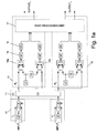
- Fig. 1a is a block diagram of a system for optimally equalizing the distortion of an optical data channel, according to an embodiment of the present invention.
- This example depicts a single polarization-channel model out of the simulated Dual-Polarization Quadrature Phase Shift Keying (DP-QPSK) 111 Gbp/s system. Only a single polarization-channel is examined (including both in-phase and quadrature components) at a baud (symbols per second) rate of 27.75 Gbaud.
- DP-QPSK Dual-Polarization Quadrature Phase Shift Keying
- the system comprises conventional optical transmitter 10 and an optical receiving end (front end) 12 of the receiver 13.
- the optical channel 11 is assumed to be linear with chromatic dispersion.
- the front end comprises a local oscillator for frequency down-conversion.
- the output of the balanced detector 14a corresponds to an in-phase (I) component and the output of the balanced detector 14b corresponds to a quadrature (Q) component.
- Each output is followed by an AAF 15 for filtering the output of each path.
- the AAF 15 can be modeled by a 5 th order Butterworth low pass filter, which reduces the analog bandwidth (BW) of the signal at each path by a factor of N, while introducing known and deterministic ISA with deterministic attributes.
- the cutoff frequency of the AAF 15 corresponds to N.
- the signal at each path is sampled and quantized by an Analog to Digital Converter (ADC) 16 at a sampling rate of 2BW/N Giga-samples/sec (in this case, 27.75 Giga-samples/sec) with 5-bit resolution.
- ADC Analog to Digital Converter
- the two I and Q paths are fed to a post processing unit 17, which performs digital post processing on the samples of each path in a processing rate which is reduced by a factor of N, as well.
- the post processing unit 17 (the processing of which represents the compensation of the distortion, which may include amplitude and phase distortions) inverts the frequency response of the channel and applies the inverse of the channel to the received signal, so as to restore the signal before the channel), and can be implemented either in the time or in the frequency domain.
- the final stage of the post processing unit is a decision block.
- the optimal decision algorithm is based on MLSE. It compensates for the deterministic ISI introduced by the AAF 15 in each path, and performs the best theoretically possible decision.
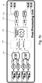
- Fig. 1B illustrates a possible implementation of the post processing unit 17, according to one embodiment.
- the post processing unit 17 may include:
- Intermediate Frequency Estimator stands for intradyne (an intradyne optical receiver has a local optical oscillator whose frequency is closer to the center frequency of the data-carrying optical carrier than the bandwidth of the data-carrying optical carrier) frequency estimator, which compensates for the imperfect wavelength alignment between the laser at the transmitter and the local oscillator laser in the receiver. This mismatch results from components variation, temperature variations, etc., and therefore, it needs to be tracked and compensated. This compensation is performed digitally in the post processing unit, which operates at 1 sample per symbol.
- the input data stream is reconstructed by optimally decoding the output of the processor using the output decoder 18, which can optimally compensate the introduced ISI.
- Fig. 2b illustrates the ONSR required for 10-3 BER as a function of AAF cutoff frequency, obtained using an FFE decoder, for several fiber lengths. It can be seen that for high CD values, the system performance is severely degraded, despite the fact that optimal sampling phase is used.
- Figs. 2a and 2b show that the MLSE is insensitive to sampling phase in a symbol-spaced system, i.e., a system with 1 Sample/symbol.
- the proposed scheme of symbol-spaced sampler enables the use of 27.75Giga-samples/sec ADCs in 111Gbps coherent digitally equalized system with full compensation of chromatic dispersion. PMD can be fully compensated in a similar manner. In addition, it allows significant VLSI hardware relaxation, reduced power consumption, and reduced cost.
Landscapes
- Physics & Mathematics (AREA)
- Electromagnetism (AREA)
- Engineering & Computer Science (AREA)
- Computer Networks & Wireless Communication (AREA)
- Signal Processing (AREA)
- Optical Communication System (AREA)
- Cable Transmission Systems, Equalization Of Radio And Reduction Of Echo (AREA)
Description
- The present invention relates to the field of coherent optical data communication. More particularly, the invention relates to a method and system for equalizing the distortion of an optical data channel, while using reduced sampling and processing rates.
- Digital compensation of Chromatic Dispersion (CD-the dependency of the phase velocity of an optical signal on its wavelength) and Polarization Mode Dispersion (PMD- modal dispersion where two different polarizations of light in a waveguide, propagate at different speeds, causing random spreading of the optical pulses) in 40 Gbp/s and 100 Gbp/s coherent optical fiber communication systems is of great interest nowadays. Today, the possibility to accurately detect not only the amplitude but also the phase of data carrying optical signals allows transmitting data by using the phase of these signals. Therefore, coherent detection and equalization allows compensating distortions that are introduced by very long fibers.
- Today, sampling of optical signals in rates of 100 Gb/s is problematic, since even though the information is carried by 28 Gb/s using different polarization and splitting the data into I and Q (In-phase and Quadrature) channels, the sampling rate must be 56 Gs/s. This requires special equipment with resolution of about 5 bits, which is expensive. In addition, there is a demand for transmitting and receiving in rages of 400 Gb/s, which pushes the limits of feasible equipment even much further.
- The common practice of CD and PMD compensation is to use fractional space equalizers, with two samples per symbol, or even more. It is well known that in undistorted media, sampling at the symbol rate forms sufficient information to recover the digital data. However, when the channel introduces linear distortions such as CD and PMD, a full reconstruction of the received analog signal is required in order to apply digital compensation. Sampling this signal at the symbol rate without preceding filtering violates the Nyquist sampling theorem, causing aliasing effect that results in performance degradation. On the other hand, using Anti Aliasing Filtering (AAF) prior to symbol rate sampling introduces substantial lowpass filtering which, in turn, causes substantial Inter Symbol Interference (ISI). The optimal equalizer, in the sense of minimum probability of error for a channel with ISI is the Maximum Likelihood Sequence Estimator (MLSE).
- The article by Fludjer et al. "Coherent Equalization and POLMUX-RZ-DQPSK for Robust 100-GE Transmission" discloses the use of a coherent digital receiver for the compensation of linear transmission impairments and polarization demultiplexing in a transmission system compatible with a future 100-Gb/s Ethernet standard. The disclosed method makes use of a standard MMSE linear equalizer, which is well known for its noise enhancement limitation, and the required bandwidth of the AAF is about 14GHz. Moreover the method is limited to CD compensation of less than +/-1000ps/nm.
- The article by KAHN J M et al: "Advanced Modulation Formats and Digital Signal Processing in Optical Communications") discloses comparisons of performance and implementation complexity of various modulation and detection techniques. Non-binary modulation with coherent detection maximizes spectral efficiency and enables effective, low-complexity digital compensation of chromatic and polarization mode dispersions and other transmission impairments. Furthermore, the article by KAHN et al discloses a method introducing detrimental SNR degradation and focusing on sampling rates higher than 1 sample per symbol. No solution for the ISI introduced by the AAF and no use of an MLSE is disclosed.
- Several attempts of dealing with symbol space equalizers were made using AAF, in order to reduce cost and complexity of VLSI implementation. However, these attempts deal only with low CD values suffer from significant power penalty due to the combined effects of Aliasing and ISI.
- All the methods described above have not yet provided satisfactory solutions to the problem of optimally equalizing the distortion of an optical data channel, while using reduced sampling and processing rates.
- It is therefore an object of the present invention to provide a method and system for optimally equalizing the distortion of an optical data channel, while using reduced sampling and processing rates.
- Another object of the present invention is to provide a method and system for equalizing the distortion of an optical data channel, without the need for expensive sampling and processing equipment.
- It is a further object of the present invention to provide a method and system for equalizing the distortion of an optical data channel, while introducing low power penalties.
- Other objects and advantages of the invention will become apparent as the description proceeds.
- The present invention is directed to a method for optimally equalizing the distortion (such as CD or PMD) of an optical data channel carrying coherent optical signals with a given analog bandwidth B. A receiving end having an I path and a Q path is provided, for receiving the optical signals and for detecting the optical signals in each path by a balanced detector. The bandwidth of the detected optical signals is reduced by a factor of N by filtering the output of each path using an AAF with a cutoff frequency which corresponds to N (and is optimized to the analog bandwidth 2B/N of each path), where the AAF has deterministic attributes and introducing known ISI. The signal is sampled at the output of each AAF by an ADC, at a sampling rate of 2B/N. Then the samples of each path are post processed by a digital processor operating at a data rate of 2B/N, such that the post processing represents the compensation of the distortion and the input data stream is reconstructed by optimally decoding the output of the processor using a Maximum Likelihood Sequence Estimator decoder (MLSE), which is capable of optimally compensating the introduced ISI.
- The MLSE decoder may be used to compensate for amplitude and phase distortions.
- Preferably, the AAF may be optimized to the analog bandwidth 2B/N of each path.
- The present invention is directed to a system for optimally equalizing the distortion (such as CD or PMD) of an optical data channel carrying coherent optical signals with a given analog bandwidth B, which comprises:
- a) a receiving end with an I path and a Q path, for receiving the optical signals and for detecting the optical signals in each path by a balanced detector;
- b) an AAF for each path with a cutoff frequency which corresponds to N, for reducing the bandwidth of the detected optical signals in the path by a factor of N by filtering the output of each path;
- c) an ADC sampling the signal at the output of each AAF at a sampling rate of 2B/N;
- d) a digital post processing unit operating at a data rate of 2B/N for post processing the samples of each path by, such that the post processing represents the compensation of the distortion; and
- e) a Maximum Likelihood Sequence Estimator decoder (MLSE) that is capable of optimally compensating the introduced ISI for reconstructing the input data stream by optimally decoding the output of the processor.
- The post processing unit may comprise:
- a) a CD equalizer, implemented in time or in frequency domain, for restoring the signal before the channel;
- b) a clock recovery unit, for retiming the received signal;
- c) a Polarization De-multiplexer, for compensating the PMD effect and de-multiplexing the two different data streams that were modulated according to the dual polarization format;
- c) an Intermediate Frequency Estimator, for restoring the intermediate frequency;
- d) a Carrier Phase Estimator, for restoring the phase of the optical carrier; and
- e) an output equalizer, for compensating the deterministic ISI introduced by the AAF in each path.
- The above and other characteristics and advantages of the invention will be better understood through the following illustrative and non-limitative detailed description of preferred embodiments thereof, with reference to the appended drawings, wherein:
-
Fig. 1a is a block diagram of a system for optimally equalizing the distortion of an optical data channel, according to an embodiment of the present invention; -
Fig. 1b illustrates a possible implementation of the post processing unit, according to one embodiment -
Fig. 2a illustrates the ONSR required for 10-3 BER as a function of AAF cutoff frequency, obtained using an MLSE decoder; and -
Fig. 2b illustrates the ONSR required for 10-3 BER as a function of AAF cutoff frequency, obtained using an FFE decoder. - The present invention proposes a coherent detection method and system with a single sample per symbol and allows lowering the information bandwidth, the sampling rate and the processing rate with very low losses regarding Optical Signal-To-Noise Ratio (OSNR). The bandwidth is reduced by Anti-Aliasing Filtering (AAF), followed by an MLSE, which is used to compensate the ISI introduced by the anti-aliasing filtering. 50,000 ps/nm of CD is fully compensated with only 1 dB penalty. The combination of AAF and MLSE allows full equalization with one sample per symbol of transmission of 111Gbps over CD of up to 50,000 ps/nm, with only 1dB of OSNR degradation.
-
Fig. 1a is a block diagram of a system for optimally equalizing the distortion of an optical data channel, according to an embodiment of the present invention. This example depicts a single polarization-channel model out of the simulated Dual-Polarization Quadrature Phase Shift Keying (DP-QPSK) 111 Gbp/s system. Only a single polarization-channel is examined (including both in-phase and quadrature components) at a baud (symbols per second) rate of 27.75 Gbaud. - The system comprises conventional
optical transmitter 10 and an optical receiving end (front end) 12 of thereceiver 13. Theoptical channel 11 is assumed to be linear with chromatic dispersion. The front end comprises a local oscillator for frequency down-conversion. The output of thebalanced detector 14a corresponds to an in-phase (I) component and the output of thebalanced detector 14b corresponds to a quadrature (Q) component. - Each output is followed by an
AAF 15 for filtering the output of each path. TheAAF 15 can be modeled by a 5th order Butterworth low pass filter, which reduces the analog bandwidth (BW) of the signal at each path by a factor of N, while introducing known and deterministic ISA with deterministic attributes. The cutoff frequency of theAAF 15 corresponds to N. - The signal at each path (at the output of each AAF) is sampled and quantized by an Analog to Digital Converter (ADC) 16 at a sampling rate of 2BW/N Giga-samples/sec (in this case, 27.75 Giga-samples/sec) with 5-bit resolution. The two I and Q paths are fed to a
post processing unit 17, which performs digital post processing on the samples of each path in a processing rate which is reduced by a factor of N, as well. The post processing unit 17 (the processing of which represents the compensation of the distortion, which may include amplitude and phase distortions) inverts the frequency response of the channel and applies the inverse of the channel to the received signal, so as to restore the signal before the channel), and can be implemented either in the time or in the frequency domain. The final stage of the post processing unit is a decision block. The optimal decision algorithm is based on MLSE. It compensates for the deterministic ISI introduced by theAAF 15 in each path, and performs the best theoretically possible decision. -
Fig. 1B illustrates a possible implementation of thepost processing unit 17, according to one embodiment. Thepost processing unit 17 may include: - a
CD equalizer 17a (CD-1 inFig. 1b ), which is designed according to a zero forcing criterion (linear equalization for restoring the signal before the channel) and can be implemented either in the time or in the frequency domain; - a
clock recovery unit 17b for retiming the received signal; - a Polarization De-multiplexer 17c for compensating the PMD effect and de-multiplexing the two different data streams that were modulated according to the dual polarization format;
- an IFE (Intermediate Frequency Estimator) 17d for restoring and cancelling the intermediate frequency;
- a CPE (Carrier Phase Estimator) 17e for restoring the phase of the optical carrier; and
- an output decoder 18 (a 16 state MLSE), in order to compensate the deterministic ISI introduced by the
AAF 15 in each path. - Intermediate Frequency Estimator stands for intradyne (an intradyne optical receiver has a local optical oscillator whose frequency is closer to the center frequency of the data-carrying optical carrier than the bandwidth of the data-carrying optical carrier) frequency estimator, which compensates for the imperfect wavelength alignment between the laser at the transmitter and the local oscillator laser in the receiver. This mismatch results from components variation, temperature variations, etc., and therefore, it needs to be tracked and compensated. This compensation is performed digitally in the post processing unit, which operates at 1 sample per symbol.
- The input data stream is reconstructed by optimally decoding the output of the processor using the
output decoder 18, which can optimally compensate the introduced ISI. - All these units operate in 1 Sample/symbol (as opposed to prior art that uses higher Samples/symbol rates).
- Several simulations have been performed, in order to determine the optimal AAF bandwidth to ensure a BER value of 10-3. In these simulations, 200,000 bits are used to ensure sufficient statistics for bit error rate (BER) of 10-3. Histogram estimation method is used for channel estimation with training sequence of 50,000 observations, which are subsequently discarded from BER calculation.
-
Fig. 2a illustrates the ONSR required for 10-3 BER as a function of AAF cutoff frequency, obtained using an MLSE decoder, for several fiber lengths. It can be seen that the proposed system with an MLSE decoder allows full compensation of CD, up to 50,000 ps/nm. Furthermore, the ISI that is introduced by the AAF is completely compensated with an OSNR degradation of 1 dB only, as compared to the case of back to back (B-t-B) transmission. While the B-t-B system with 19GHz AAF cutoff frequency requires 13.7 dB of OSNR for BER of 10-3, the case of CD=50,000 ps/nm reaches the same BER value with 14.7dB of OSNR. Also, for AAF cutoff frequency values higher than 11G Hz, the aliasing effect leads to performance degradation which can not be compensated by the MLSE, emphasizing the requirement of using an AAF in a symbol-spaced sampling system. -
Fig. 2b illustrates the ONSR required for 10-3 BER as a function of AAF cutoff frequency, obtained using an FFE decoder, for several fiber lengths. It can be seen that for high CD values, the system performance is severely degraded, despite the fact that optimal sampling phase is used. -
Figs. 2a and 2b show that the MLSE is insensitive to sampling phase in a symbol-spaced system, i.e., a system with 1 Sample/symbol. The proposed scheme of symbol-spaced sampler enables the use of 27.75Giga-samples/sec ADCs in 111Gbps coherent digitally equalized system with full compensation of chromatic dispersion. PMD can be fully compensated in a similar manner. In addition, it allows significant VLSI hardware relaxation, reduced power consumption, and reduced cost. - The above examples and description have of course been provided only for the purpose of illustration, and are not intended to limit the invention in any way. As will be appreciated by the skilled person, the invention can be carried out in a great variety of ways, employing more than one technique from those described above, all without exceeding the scope of the invention.
Claims (10)
- A method for optimally equalizing distortion of an optical data channel (11) carrying coherent optical signals with a given analog bandwidth B1 [GHz] and a given symbol rate B2 [GSymbols/sec], comprising:a) providing a receiving end with a balanced detector (14a, 14b), for receiving and detecting said optical signals;b) reducing the analog bandwidth B1 of detected optical signals by a factor of N by filtering said optical signals using an Anti-Aliasing Filter (15) with a cutoff frequency which corresponds to N, said Anti-Aliasing Filter (15) having deterministic attributes and introducing known deterministic Inter Symbol Interference (ISI);c) sampling said optical signals at the output of said Anti-Aliasing Filter (15) by an Analog to Digital Converter (16), using a sampling rate of a single sample per symbol;d) post processing the sampled optical signals by a digital processor (17) operating at a processing rate being equal to said sampling rate and to said symbol rate B2, such that said post processing represents compensation of said distortion; ande) reconstructing an input data stream by:e.1) inverting a frequency response of said channel and applying an inverse of the channel to said optical signal received after said post processing, to compensate for channel distortions of Chromatic Dispersion (CD), Polarization Mode Dispersion (PMD), timing errors, and amplitude and phase distortions, except for the Inter Symbol Interference (ISI) introduced by said Anti-Aliasing Filter (15); ande.2) optimally decoding the output of said digital processor (17) using a Maximum Likelihood Sequence Estimator - MLSE (18) decoder being capable of optimally compensating the known deterministic Inter Symbol Interference, introduced by said Anti-Aliasing Filter (15).
- A method according to claim 1, wherein the distortion of the data channel is Chromatic Dispersion.
- A method according to claim 1, wherein the distortion of the data channel is Polarization Mode Dispersion.
- A method according to claim 1, wherein the MLSE decoder (18) compensates for amplitude and phase distortions.
- A method according to claim 1, wherein the Anti-Aliasing Filter (15) is optimized to an analog bandwidth B1/N by selecting the cutoff frequency of said Anti-Aliasing Filter (15) to correspond to N.
- A system for optimally equalizing distortion of an optical data channel (11) carrying coherent optical signals with a given analog bandwidth B1 [GHz] and a given symbol rate B2 [GSymbols/sec], comprising:a) a receiving end (13) with a balanced detector (14a, 14b), for receiving and detecting said optical signals;b) an Anti-Aliasing Filter (15) with a cutoff frequency which corresponds to N, for reducing the bandwidth of detected optical signals by a factor of N by filtering said optical signals;c) an Analog to Digital Converter (16) for sampling said optical signals at the output of said Anti-Aliasing Filter (15) using a sampling rate of a single sample per symbol; andd) a digital post processing unit (17) with a processor (17) operating at a processing rate being equal to said sampling rate and to said symbol rate, for:d.1) inverting a frequency response of said channel and applying an inverse of the channel to said received optical signals, to compensate for channel distortions, of chromatic dispersion, polarization mode dispersion, timing errors, amplitude and phase distortions except for an Inter Symbol Interference (ISI) introduced by said Anti-Aliasing Filter (15);d.2) post processing the samples, such that said digital post processing represents compensation of said distortion;wherein said digital post processing unit (17) comprises a Maximum Likelihood Sequence Estimator - MLSE (18) decoder being capable of reconstructing an input data stream by optimally compensating known deterministic Inter Symbol Interference, introduced by said Anti-Aliasing Filter (15), and reconstructing an input data stream and to optimally decode the output of said processor (17);
said digital processing unit (17) further comprises:a) a Chromatic Dispersion (CD) equalizer (17a), implemented in time or in frequency domain, for restoring a signal before the channel;b) a clock recovery unit (17b), for retiming a received signal;c) a Polarization De-multiplexer (17c), for compensating Polarization Mode Dispersion effects and de-multiplexing different data streams that were modulated according to the dual polarization format;d) an Intermediate Frequency Estimator (17d), for restoring an intermediate frequency; ande) a Carrier Phase Estimator (17e), for restoring a phase of the optical carrier. - A system according to claim 6, in which the distortion of the data channel is Chromatic Dispersion.
- A system according to claim 6, in which the distortion of the data channel is Polarization Mode Dispersion.
- A system according to claim 6, in which the MLSE decoder (18) compensates for amplitude and phase distortions.
- A system according to claim 6, in which the Anti-Aliasing Filter (15) is optimized to an analog bandwidth of B1/N by selecting the cutoff frequency of said Anti-Aliasing Filter (15) to correspond to N.
Applications Claiming Priority (2)
| Application Number | Priority Date | Filing Date | Title |
|---|---|---|---|
| US28640009P | 2009-12-15 | 2009-12-15 | |
| PCT/IL2010/001046 WO2011073974A1 (en) | 2009-12-15 | 2010-12-13 | Method and system for coherent equalization of chromatic dispersion of optical signals in a fiber |
Publications (3)
| Publication Number | Publication Date |
|---|---|
| EP2514093A1 EP2514093A1 (en) | 2012-10-24 |
| EP2514093A4 EP2514093A4 (en) | 2015-09-02 |
| EP2514093B1 true EP2514093B1 (en) | 2018-01-24 |
Family
ID=44166814
Family Applications (1)
| Application Number | Title | Priority Date | Filing Date |
|---|---|---|---|
| EP10837158.4A Not-in-force EP2514093B1 (en) | 2009-12-15 | 2010-12-13 | Method and system for coherent equalization of chromatic dispersion of optical signals in a fiber |
Country Status (5)
| Country | Link |
|---|---|
| US (1) | US9537578B2 (en) |
| EP (1) | EP2514093B1 (en) |
| JP (1) | JP2013514027A (en) |
| CN (1) | CN102204132B (en) |
| WO (1) | WO2011073974A1 (en) |
Families Citing this family (20)
| Publication number | Priority date | Publication date | Assignee | Title |
|---|---|---|---|---|
| WO2012090190A1 (en) * | 2010-11-08 | 2012-07-05 | Ben-Gurion University Of The Negev Research & Development Authority | A low cost direct modulation and coherent detection system |
| US9426000B2 (en) | 2012-01-06 | 2016-08-23 | Multiply Ltd. | Symbol spaced adaptive MIMO equalization for ultra high bit rate optical communication systems |
| HK1202002A1 (en) * | 2012-02-10 | 2015-09-11 | 中兴通讯(美国)公司 | System and method for coherent detection with digital signal procession |
| JP2013183455A (en) * | 2012-02-29 | 2013-09-12 | Zte (Usa) Inc | Nyquist wavelength division multiplexing system |
| US8886058B2 (en) * | 2012-06-04 | 2014-11-11 | Cisco Technology, Inc. | Cycle slip reduction in coherent optical communications |
| CN103634054B (en) * | 2012-08-23 | 2016-01-20 | 北京邮电大学 | Linear damage for high speed coherent reception system compensates and polarization demultiplexing method |
| CN103401616B (en) * | 2013-08-06 | 2015-08-26 | 电子科技大学 | A kind of radio frequency optical transmission system of high linearity and method |
| JP6269841B2 (en) | 2014-08-28 | 2018-01-31 | 日本電気株式会社 | Polarization dispersion adder and optical receiver |
| CN105610517B (en) * | 2014-11-14 | 2018-05-08 | 中兴通讯股份有限公司 | The iteration post-equalization of coherent optical heterodyne communicatio |
| US9887729B2 (en) * | 2014-11-21 | 2018-02-06 | Nec Corporation | RF sub-band de-multiplexing for ultra-wide band optical digital coherent detection |
| CN106330322B (en) * | 2015-06-30 | 2019-02-05 | 深圳市中兴微电子技术有限公司 | Frequency offset phase offset processing method and device |
| CN106896619A (en) * | 2015-12-17 | 2017-06-27 | 中国航天科工集团八五研究所 | Analog-digital commutator and method based on photon stretching |
| CN105681237B (en) * | 2016-01-15 | 2018-10-16 | 电子科技大学 | A method of intersymbol interference is inhibited by digital light preequalization method |
| JP6315040B2 (en) * | 2016-08-29 | 2018-04-25 | Nttエレクトロニクス株式会社 | Optical transmission distortion compensation apparatus, optical transmission distortion compensation method, and communication apparatus |
| US10128959B1 (en) * | 2016-10-24 | 2018-11-13 | Inphi Corporation | Tap centerer method and structure for coherent optical receiver |
| CN109981500B (en) * | 2017-12-28 | 2023-04-28 | 海思光电子有限公司 | Signal processing method and signal processing device |
| CN112314007B (en) * | 2018-04-20 | 2024-04-23 | 瑞典爱立信有限公司 | Method and apparatus for energy-efficient transmission and reception of signals using aliasing |
| CN115001591B (en) * | 2022-05-25 | 2023-08-04 | 西安交通大学 | High-speed analog multiplexer for coherent light detection of more than 100G |
| CN115242584B (en) * | 2022-07-21 | 2023-12-01 | 苏州大学 | Method and device for optimizing complexity of MLSE algorithm based on lookup table |
| CN119916340B (en) * | 2025-04-07 | 2025-07-08 | 南京信息工程大学 | A Balance Detection Device Based on Digital Post-Processing |
Family Cites Families (18)
| Publication number | Priority date | Publication date | Assignee | Title |
|---|---|---|---|---|
| EP0316876B1 (en) * | 1987-11-16 | 1994-01-26 | Nec Corporation | A digital signal receiving circuit with means for controlling a baud rate sampling phase by a power of sampled signals |
| US5276712A (en) * | 1989-11-16 | 1994-01-04 | Digital Equipment Corporation | Method and apparatus for clock recovery in digital communication systems |
| US5889827A (en) * | 1996-12-12 | 1999-03-30 | Ericsson Inc. | Method and apparatus for digital symbol detection using medium response estimates |
| US6574293B1 (en) * | 1998-10-28 | 2003-06-03 | Ericsson Inc. | Receivers and methods for reducing interference in radio communications |
| DE50107714D1 (en) * | 2000-10-09 | 2006-02-23 | Reinhold Noe | ARRANGEMENT AND METHOD FOR OPTICAL INFORMATION TRANSMISSION |
| US7031405B1 (en) * | 2000-11-15 | 2006-04-18 | Ati Research, Inc. | Carrier phase estimation based on single-axis constant modulus cost criterion and Bussgang criteria |
| US7460793B2 (en) * | 2002-12-11 | 2008-12-02 | Michael George Taylor | Coherent optical detection and signal processing method and system |
| US6778317B1 (en) * | 2003-02-19 | 2004-08-17 | The Aerospace Corporation | Optical fiber quadrature demodulator |
| US7266310B1 (en) * | 2003-04-29 | 2007-09-04 | Nortel Networks Limited | Digital compensation for optical transmission system |
| US7209664B1 (en) * | 2003-06-10 | 2007-04-24 | Nortel Networks Limited | Frequency agile transmitter and receiver architecture for DWDM systems |
| US7233632B1 (en) * | 2003-08-21 | 2007-06-19 | L-3 Communications Corporation | Symbol timing correction for a phase modulated signal with mutually interfering symbols |
| US7522847B2 (en) * | 2003-12-19 | 2009-04-21 | Broadcom Corporation | Continuous time filter-decision feedback equalizer architecture for optical channel equalization |
| US7522842B1 (en) * | 2005-09-30 | 2009-04-21 | Nortel Networks Limited | Optical transmission system using Raman amplification |
| GB0606489D0 (en) | 2006-03-31 | 2006-05-10 | Qinetiq Ltd | System and method for processing imagery from synthetic aperture systems |
| US8787771B2 (en) * | 2006-10-06 | 2014-07-22 | Ciena Corporation | All-optical regenerator and optical network incorporating same |
| US7970289B2 (en) * | 2007-03-14 | 2011-06-28 | Opnext Subsystems, Inc. | GT decoder having bandwidth control for ISI compensation |
| CN101442364B (en) | 2007-11-19 | 2011-10-19 | 富士通株式会社 | Light coherent receiver, frequency difference estimation apparatus and method for light coherent receiver |
| US20100296819A1 (en) * | 2008-04-24 | 2010-11-25 | Kahn Joseph M | Optical Receivers and Communication Systems |
-
2010
- 2010-12-13 US US13/515,397 patent/US9537578B2/en not_active Expired - Fee Related
- 2010-12-13 CN CN201080003104.8A patent/CN102204132B/en not_active Expired - Fee Related
- 2010-12-13 WO PCT/IL2010/001046 patent/WO2011073974A1/en not_active Ceased
- 2010-12-13 JP JP2012543994A patent/JP2013514027A/en active Pending
- 2010-12-13 EP EP10837158.4A patent/EP2514093B1/en not_active Not-in-force
Non-Patent Citations (1)
| Title |
|---|
| None * |
Also Published As
| Publication number | Publication date |
|---|---|
| EP2514093A1 (en) | 2012-10-24 |
| US9537578B2 (en) | 2017-01-03 |
| CN102204132B (en) | 2014-10-15 |
| CN102204132A (en) | 2011-09-28 |
| WO2011073974A1 (en) | 2011-06-23 |
| JP2013514027A (en) | 2013-04-22 |
| HK1158844A1 (en) | 2012-07-20 |
| EP2514093A4 (en) | 2015-09-02 |
| US20120251112A1 (en) | 2012-10-04 |
Similar Documents
| Publication | Publication Date | Title |
|---|---|---|
| US9537578B2 (en) | Method and system for coherent equalization of chromatic dispersion of optical signals in a fiber | |
| CN102215189B (en) | Filter, coherent receiver and coherent reception method | |
| US8335438B2 (en) | Estimating frequency offset using a feedback loop | |
| US8855501B2 (en) | Method for carrier frequency recovery and optical intradyne coherent receiver | |
| EP2613452B1 (en) | Digital filter device, digital filtering method, and control program for digital filter device | |
| US8559828B2 (en) | Frame formatting for high rate optical communications | |
| US9426000B2 (en) | Symbol spaced adaptive MIMO equalization for ultra high bit rate optical communication systems | |
| Li et al. | Spectrally efficient quadrature duobinary coherent systems with symbol-rate digital signal processing | |
| Zhou et al. | Digital signal processing for coherent optical communication | |
| Gorshtein et al. | Coherent CD equalization for 111Gbps DP-QPSK with one sample per symbol based on anti-aliasing filtering and MLSE | |
| Gorshtein et al. | Coherent compensation for 100G DP-QPSK with one sample per symbol based on antialiasing filtering and blind equalization MLSE | |
| US7474860B2 (en) | Optimum sample spacing in over-sampled maximum likelihood sequence estimation receivers | |
| Gorshtein et al. | Advanced modulation formats and digital signal processing for fiber optic communication | |
| Zhu et al. | Optoelectronic feedforward equalization: simple 1-tap optical delay line and Ethernet-compliant linear FFE enabling C-band 100G PAM4 over ER+ distance | |
| HK1158844B (en) | Method and system for coherent equalization of chromatic dispersion of optical signals in a fiber | |
| Hauske et al. | Iterative electronic equalization utilizing low complexity MLSEs for 40 Gbit/s DQPSK modulation | |
| Fatadin et al. | DSP techniques for 16-QAM coherent optical systems | |
| Savory et al. | Ultra long-haul qpsk transmission using a digital coherent receiver | |
| Zhang et al. | ADC bandwidth optimization in coherent optical polarization multiplexing quadrature phase-shift keying system | |
| Chen et al. | Training aided frequency domain equalization with maximum-likelihood sequence detection in coherent optical communications systems using FTN signaling | |
| Zhang et al. | Low-Complexity Monitoring and Compensation of Transceiver IQ Imbalance by Multi-dimensional Architecture for Dual-Polarization 16 Quadrature Amplitude Modulation | |
| Hauske et al. | Reduced complexity Rx concepts for optical multilevel transmission | |
| EP2362557B1 (en) | MLSE in coherent optical receiver for optical filtering tolerance | |
| Rosa et al. | 112 Gb/s DP-QPSK coherent optical transmission over 3000 km using an complete set of digital signal processing algorithms | |
| Li et al. | Chromatic dispersion compensation of OOK signals with MLSE utilizing diverse VSB filtering |
Legal Events
| Date | Code | Title | Description |
|---|---|---|---|
| PUAI | Public reference made under article 153(3) epc to a published international application that has entered the european phase |
Free format text: ORIGINAL CODE: 0009012 |
|
| 17P | Request for examination filed |
Effective date: 20120713 |
|
| AK | Designated contracting states |
Kind code of ref document: A1 Designated state(s): AL AT BE BG CH CY CZ DE DK EE ES FI FR GB GR HR HU IE IS IT LI LT LU LV MC MK MT NL NO PL PT RO RS SE SI SK SM TR |
|
| DAX | Request for extension of the european patent (deleted) | ||
| RA4 | Supplementary search report drawn up and despatched (corrected) |
Effective date: 20150805 |
|
| RIC1 | Information provided on ipc code assigned before grant |
Ipc: H04B 10/61 20130101ALI20150730BHEP Ipc: H03H 7/30 20060101AFI20150730BHEP |
|
| 17Q | First examination report despatched |
Effective date: 20160704 |
|
| GRAP | Despatch of communication of intention to grant a patent |
Free format text: ORIGINAL CODE: EPIDOSNIGR1 |
|
| INTG | Intention to grant announced |
Effective date: 20170816 |
|
| GRAS | Grant fee paid |
Free format text: ORIGINAL CODE: EPIDOSNIGR3 |
|
| GRAA | (expected) grant |
Free format text: ORIGINAL CODE: 0009210 |
|
| AK | Designated contracting states |
Kind code of ref document: B1 Designated state(s): AL AT BE BG CH CY CZ DE DK EE ES FI FR GB GR HR HU IE IS IT LI LT LU LV MC MK MT NL NO PL PT RO RS SE SI SK SM TR |
|
| REG | Reference to a national code |
Ref country code: GB Ref legal event code: FG4D |
|
| REG | Reference to a national code |
Ref country code: CH Ref legal event code: EP |
|
| REG | Reference to a national code |
Ref country code: AT Ref legal event code: REF Ref document number: 966316 Country of ref document: AT Kind code of ref document: T Effective date: 20180215 |
|
| REG | Reference to a national code |
Ref country code: IE Ref legal event code: FG4D |
|
| REG | Reference to a national code |
Ref country code: DE Ref legal event code: R096 Ref document number: 602010048287 Country of ref document: DE |
|
| REG | Reference to a national code |
Ref country code: NL Ref legal event code: MP Effective date: 20180124 |
|
| REG | Reference to a national code |
Ref country code: LT Ref legal event code: MG4D |
|
| REG | Reference to a national code |
Ref country code: AT Ref legal event code: MK05 Ref document number: 966316 Country of ref document: AT Kind code of ref document: T Effective date: 20180124 |
|
| PG25 | Lapsed in a contracting state [announced via postgrant information from national office to epo] |
Ref country code: NL Free format text: LAPSE BECAUSE OF FAILURE TO SUBMIT A TRANSLATION OF THE DESCRIPTION OR TO PAY THE FEE WITHIN THE PRESCRIBED TIME-LIMIT Effective date: 20180124 |
|
| PG25 | Lapsed in a contracting state [announced via postgrant information from national office to epo] |
Ref country code: NO Free format text: LAPSE BECAUSE OF FAILURE TO SUBMIT A TRANSLATION OF THE DESCRIPTION OR TO PAY THE FEE WITHIN THE PRESCRIBED TIME-LIMIT Effective date: 20180424 Ref country code: CY Free format text: LAPSE BECAUSE OF FAILURE TO SUBMIT A TRANSLATION OF THE DESCRIPTION OR TO PAY THE FEE WITHIN THE PRESCRIBED TIME-LIMIT Effective date: 20180124 Ref country code: HR Free format text: LAPSE BECAUSE OF FAILURE TO SUBMIT A TRANSLATION OF THE DESCRIPTION OR TO PAY THE FEE WITHIN THE PRESCRIBED TIME-LIMIT Effective date: 20180124 Ref country code: ES Free format text: LAPSE BECAUSE OF FAILURE TO SUBMIT A TRANSLATION OF THE DESCRIPTION OR TO PAY THE FEE WITHIN THE PRESCRIBED TIME-LIMIT Effective date: 20180124 Ref country code: LT Free format text: LAPSE BECAUSE OF FAILURE TO SUBMIT A TRANSLATION OF THE DESCRIPTION OR TO PAY THE FEE WITHIN THE PRESCRIBED TIME-LIMIT Effective date: 20180124 Ref country code: FI Free format text: LAPSE BECAUSE OF FAILURE TO SUBMIT A TRANSLATION OF THE DESCRIPTION OR TO PAY THE FEE WITHIN THE PRESCRIBED TIME-LIMIT Effective date: 20180124 |
|
| PG25 | Lapsed in a contracting state [announced via postgrant information from national office to epo] |
Ref country code: GR Free format text: LAPSE BECAUSE OF FAILURE TO SUBMIT A TRANSLATION OF THE DESCRIPTION OR TO PAY THE FEE WITHIN THE PRESCRIBED TIME-LIMIT Effective date: 20180425 Ref country code: PL Free format text: LAPSE BECAUSE OF FAILURE TO SUBMIT A TRANSLATION OF THE DESCRIPTION OR TO PAY THE FEE WITHIN THE PRESCRIBED TIME-LIMIT Effective date: 20180124 Ref country code: LV Free format text: LAPSE BECAUSE OF FAILURE TO SUBMIT A TRANSLATION OF THE DESCRIPTION OR TO PAY THE FEE WITHIN THE PRESCRIBED TIME-LIMIT Effective date: 20180124 Ref country code: AT Free format text: LAPSE BECAUSE OF FAILURE TO SUBMIT A TRANSLATION OF THE DESCRIPTION OR TO PAY THE FEE WITHIN THE PRESCRIBED TIME-LIMIT Effective date: 20180124 Ref country code: IS Free format text: LAPSE BECAUSE OF FAILURE TO SUBMIT A TRANSLATION OF THE DESCRIPTION OR TO PAY THE FEE WITHIN THE PRESCRIBED TIME-LIMIT Effective date: 20180524 Ref country code: SE Free format text: LAPSE BECAUSE OF FAILURE TO SUBMIT A TRANSLATION OF THE DESCRIPTION OR TO PAY THE FEE WITHIN THE PRESCRIBED TIME-LIMIT Effective date: 20180124 Ref country code: BG Free format text: LAPSE BECAUSE OF FAILURE TO SUBMIT A TRANSLATION OF THE DESCRIPTION OR TO PAY THE FEE WITHIN THE PRESCRIBED TIME-LIMIT Effective date: 20180424 Ref country code: RS Free format text: LAPSE BECAUSE OF FAILURE TO SUBMIT A TRANSLATION OF THE DESCRIPTION OR TO PAY THE FEE WITHIN THE PRESCRIBED TIME-LIMIT Effective date: 20180124 |
|
| REG | Reference to a national code |
Ref country code: DE Ref legal event code: R097 Ref document number: 602010048287 Country of ref document: DE |
|
| PG25 | Lapsed in a contracting state [announced via postgrant information from national office to epo] |
Ref country code: AL Free format text: LAPSE BECAUSE OF FAILURE TO SUBMIT A TRANSLATION OF THE DESCRIPTION OR TO PAY THE FEE WITHIN THE PRESCRIBED TIME-LIMIT Effective date: 20180124 Ref country code: RO Free format text: LAPSE BECAUSE OF FAILURE TO SUBMIT A TRANSLATION OF THE DESCRIPTION OR TO PAY THE FEE WITHIN THE PRESCRIBED TIME-LIMIT Effective date: 20180124 Ref country code: IT Free format text: LAPSE BECAUSE OF FAILURE TO SUBMIT A TRANSLATION OF THE DESCRIPTION OR TO PAY THE FEE WITHIN THE PRESCRIBED TIME-LIMIT Effective date: 20180124 Ref country code: EE Free format text: LAPSE BECAUSE OF FAILURE TO SUBMIT A TRANSLATION OF THE DESCRIPTION OR TO PAY THE FEE WITHIN THE PRESCRIBED TIME-LIMIT Effective date: 20180124 |
|
| PG25 | Lapsed in a contracting state [announced via postgrant information from national office to epo] |
Ref country code: CZ Free format text: LAPSE BECAUSE OF FAILURE TO SUBMIT A TRANSLATION OF THE DESCRIPTION OR TO PAY THE FEE WITHIN THE PRESCRIBED TIME-LIMIT Effective date: 20180124 Ref country code: SM Free format text: LAPSE BECAUSE OF FAILURE TO SUBMIT A TRANSLATION OF THE DESCRIPTION OR TO PAY THE FEE WITHIN THE PRESCRIBED TIME-LIMIT Effective date: 20180124 Ref country code: DK Free format text: LAPSE BECAUSE OF FAILURE TO SUBMIT A TRANSLATION OF THE DESCRIPTION OR TO PAY THE FEE WITHIN THE PRESCRIBED TIME-LIMIT Effective date: 20180124 Ref country code: SK Free format text: LAPSE BECAUSE OF FAILURE TO SUBMIT A TRANSLATION OF THE DESCRIPTION OR TO PAY THE FEE WITHIN THE PRESCRIBED TIME-LIMIT Effective date: 20180124 |
|
| PLBE | No opposition filed within time limit |
Free format text: ORIGINAL CODE: 0009261 |
|
| STAA | Information on the status of an ep patent application or granted ep patent |
Free format text: STATUS: NO OPPOSITION FILED WITHIN TIME LIMIT |
|
| 26N | No opposition filed |
Effective date: 20181025 |
|
| PG25 | Lapsed in a contracting state [announced via postgrant information from national office to epo] |
Ref country code: SI Free format text: LAPSE BECAUSE OF FAILURE TO SUBMIT A TRANSLATION OF THE DESCRIPTION OR TO PAY THE FEE WITHIN THE PRESCRIBED TIME-LIMIT Effective date: 20180124 |
|
| REG | Reference to a national code |
Ref country code: CH Ref legal event code: PL |
|
| PG25 | Lapsed in a contracting state [announced via postgrant information from national office to epo] |
Ref country code: MC Free format text: LAPSE BECAUSE OF FAILURE TO SUBMIT A TRANSLATION OF THE DESCRIPTION OR TO PAY THE FEE WITHIN THE PRESCRIBED TIME-LIMIT Effective date: 20180124 Ref country code: LU Free format text: LAPSE BECAUSE OF NON-PAYMENT OF DUE FEES Effective date: 20181213 |
|
| REG | Reference to a national code |
Ref country code: IE Ref legal event code: MM4A |
|
| REG | Reference to a national code |
Ref country code: BE Ref legal event code: MM Effective date: 20181231 |
|
| PG25 | Lapsed in a contracting state [announced via postgrant information from national office to epo] |
Ref country code: IE Free format text: LAPSE BECAUSE OF NON-PAYMENT OF DUE FEES Effective date: 20181213 |
|
| PG25 | Lapsed in a contracting state [announced via postgrant information from national office to epo] |
Ref country code: BE Free format text: LAPSE BECAUSE OF NON-PAYMENT OF DUE FEES Effective date: 20181231 |
|
| PG25 | Lapsed in a contracting state [announced via postgrant information from national office to epo] |
Ref country code: CH Free format text: LAPSE BECAUSE OF NON-PAYMENT OF DUE FEES Effective date: 20181231 Ref country code: LI Free format text: LAPSE BECAUSE OF NON-PAYMENT OF DUE FEES Effective date: 20181231 |
|
| PG25 | Lapsed in a contracting state [announced via postgrant information from national office to epo] |
Ref country code: MT Free format text: LAPSE BECAUSE OF NON-PAYMENT OF DUE FEES Effective date: 20181213 |
|
| PG25 | Lapsed in a contracting state [announced via postgrant information from national office to epo] |
Ref country code: TR Free format text: LAPSE BECAUSE OF FAILURE TO SUBMIT A TRANSLATION OF THE DESCRIPTION OR TO PAY THE FEE WITHIN THE PRESCRIBED TIME-LIMIT Effective date: 20180124 |
|
| PG25 | Lapsed in a contracting state [announced via postgrant information from national office to epo] |
Ref country code: PT Free format text: LAPSE BECAUSE OF FAILURE TO SUBMIT A TRANSLATION OF THE DESCRIPTION OR TO PAY THE FEE WITHIN THE PRESCRIBED TIME-LIMIT Effective date: 20180124 |
|
| PG25 | Lapsed in a contracting state [announced via postgrant information from national office to epo] |
Ref country code: HU Free format text: LAPSE BECAUSE OF FAILURE TO SUBMIT A TRANSLATION OF THE DESCRIPTION OR TO PAY THE FEE WITHIN THE PRESCRIBED TIME-LIMIT; INVALID AB INITIO Effective date: 20101213 Ref country code: MK Free format text: LAPSE BECAUSE OF NON-PAYMENT OF DUE FEES Effective date: 20180124 |
|
| P01 | Opt-out of the competence of the unified patent court (upc) registered |
Effective date: 20230530 |
|
| PGFP | Annual fee paid to national office [announced via postgrant information from national office to epo] |
Ref country code: FR Payment date: 20230622 Year of fee payment: 13 Ref country code: DE Payment date: 20230627 Year of fee payment: 13 |
|
| PGFP | Annual fee paid to national office [announced via postgrant information from national office to epo] |
Ref country code: GB Payment date: 20230619 Year of fee payment: 13 |
|
| REG | Reference to a national code |
Ref country code: DE Ref legal event code: R119 Ref document number: 602010048287 Country of ref document: DE |
|
| GBPC | Gb: european patent ceased through non-payment of renewal fee |
Effective date: 20231213 |
|
| PG25 | Lapsed in a contracting state [announced via postgrant information from national office to epo] |
Ref country code: DE Free format text: LAPSE BECAUSE OF NON-PAYMENT OF DUE FEES Effective date: 20240702 |
|
| PG25 | Lapsed in a contracting state [announced via postgrant information from national office to epo] |
Ref country code: GB Free format text: LAPSE BECAUSE OF NON-PAYMENT OF DUE FEES Effective date: 20231213 |
|
| PG25 | Lapsed in a contracting state [announced via postgrant information from national office to epo] |
Ref country code: FR Free format text: LAPSE BECAUSE OF NON-PAYMENT OF DUE FEES Effective date: 20231231 |
|
| PG25 | Lapsed in a contracting state [announced via postgrant information from national office to epo] |
Ref country code: GB Free format text: LAPSE BECAUSE OF NON-PAYMENT OF DUE FEES Effective date: 20231213 Ref country code: FR Free format text: LAPSE BECAUSE OF NON-PAYMENT OF DUE FEES Effective date: 20231231 Ref country code: DE Free format text: LAPSE BECAUSE OF NON-PAYMENT OF DUE FEES Effective date: 20240702 |