EP2511912A2 - Diffraction grating for X-ray Talbot interferometer, method of manufacturing the same, and X-ray Talbot interferometer - Google Patents
Diffraction grating for X-ray Talbot interferometer, method of manufacturing the same, and X-ray Talbot interferometer Download PDFInfo
- Publication number
- EP2511912A2 EP2511912A2 EP12164092A EP12164092A EP2511912A2 EP 2511912 A2 EP2511912 A2 EP 2511912A2 EP 12164092 A EP12164092 A EP 12164092A EP 12164092 A EP12164092 A EP 12164092A EP 2511912 A2 EP2511912 A2 EP 2511912A2
- Authority
- EP
- European Patent Office
- Prior art keywords
- diffraction grating
- ray
- talbot interferometer
- ray talbot
- metal film
- Prior art date
- Legal status (The legal status is an assumption and is not a legal conclusion. Google has not performed a legal analysis and makes no representation as to the accuracy of the status listed.)
- Granted
Links
Images


Classifications
-
- G—PHYSICS
- G21—NUCLEAR PHYSICS; NUCLEAR ENGINEERING
- G21K—HANDLING OF PARTICLES OR IONISING RADIATION NOT OTHERWISE PROVIDED FOR; IRRADIATION DEVICES; GAMMA RAY OR X-RAY MICROSCOPES
- G21K1/00—Arrangements for handling particles or ionising radiation, e.g. focusing or moderating
- G21K1/06—Arrangements for handling particles or ionising radiation, e.g. focusing or moderating using diffraction, refraction or reflection, e.g. monochromators
-
- G—PHYSICS
- G21—NUCLEAR PHYSICS; NUCLEAR ENGINEERING
- G21K—HANDLING OF PARTICLES OR IONISING RADIATION NOT OTHERWISE PROVIDED FOR; IRRADIATION DEVICES; GAMMA RAY OR X-RAY MICROSCOPES
- G21K1/00—Arrangements for handling particles or ionising radiation, e.g. focusing or moderating
- G21K1/06—Arrangements for handling particles or ionising radiation, e.g. focusing or moderating using diffraction, refraction or reflection, e.g. monochromators
- G21K1/062—Devices having a multilayer structure
-
- G—PHYSICS
- G21—NUCLEAR PHYSICS; NUCLEAR ENGINEERING
- G21K—HANDLING OF PARTICLES OR IONISING RADIATION NOT OTHERWISE PROVIDED FOR; IRRADIATION DEVICES; GAMMA RAY OR X-RAY MICROSCOPES
- G21K2207/00—Particular details of imaging devices or methods using ionizing electromagnetic radiation such as X-rays or gamma rays
- G21K2207/005—Methods and devices obtaining contrast from non-absorbing interaction of the radiation with matter, e.g. phase contrast
Definitions
- the present invention relates to a diffraction grating for an X-ray Talbot interferometer, a method of manufacturing the same, and an X-ray Talbot interferometer.
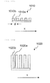
- the X-ray Talbot interferometer 1000 includes a first diffraction grating 1010, a second diffraction grating 1020, and an X-ray image detector 30 (see International Patent WO 2004/58070 A ). As illustrated in FIGS. 10A and 10B , the first diffraction grating 1010 and the second diffraction grating 1020 have grooves 1010a and 1020a formed in a metal plate at predetermined intervals in one direction.
- the groove transmits the X-ray, while a ridge portion 1010b between neighboring grooves transmits the X-ray after shifting the phase by ⁇ /2, and a ridge portion 1020b blocks (absorbs) the X-ray.
- gold (Au) having high X-ray absorbing power is usually used.
- the X-ray Talbot interferometer when the X-ray is irradiated from an X-ray source to the first diffraction grating via a sample, the X-ray transmitted through the groove portion 1010a and the X-ray transmitted and diffracted through the ridge portion 1010b interfere with each other. Then, self images of the first diffraction grating 1010 are formed at positions of integral multiples of a Talbot distance d2/2 ⁇ of the first diffraction grating 1010 (d represents a period of the diffraction grating, and ⁇ represents a wavelength of the X-ray) as the Talbot effect.
- the self image has a distortion due to a sample 4, and the distortion has information of the sample.
- the second diffraction grating 1020 is disposed at a position where the self image of the first diffraction grating 1010 is formed. Then, a distribution of the X-ray transmitted through the second diffraction grating 1020 has moire fringes because the first self image is overlaid. Therefore, this X-ray distribution is detected by the X-ray image detector, and image analysis is performed so that an image of the sample 4 is obtained.
- the groove portion 1020a of the second diffraction grating 1020 have a high X-ray transmittance, while the ridge portion 1020b have a low X-ray transmittance. Therefore, it is preferred that the second diffraction grating 1020 be an amplitude diffraction grating having a larger thickness than the first diffraction grating 1010.
- the thickness of the ridge portion is required to be approximately 10 ⁇ m or smaller.
- the contrast of the self image becomes highest when a phase shift amount becomes ⁇ /2. Therefore, in order to realize this, it is necessary to set a thickness of the ridge portion (depth of the groove) at approximately 1 to 10 ⁇ m, and fine machining and manufacturing technique are required.
- the groove portion 1020a of the diffraction grating have a high X-ray transmittance and the ridge portion 1020b have a low X-ray transmittance. Therefore, it is required to form the groove to have a large depth of approximately 10 to 100 ⁇ m even when gold is used. Therefore, an aspect ratio expressed by (depth of groove)/(width of groove) of the diffraction grating becomes very large, and hence production of the diffraction grating becomes difficult.
- a technique including the steps of patterning and removing a photosensitive resin on a surface of a silicon substrate by a lithography method, etching the silicon substrate, from which the photosensitive resin is removed, by an ICP plasma etching method so as to form a slit groove, then depositing an insulator material in the slit groove, further etching the remaining photosensitive resin and the silicon substrate by the ICP plasma etching method so as to form a second slit groove, and forming an X-ray absorbing metal portion in the second slit groove by the electroforming method (see Japanese Patent Application Laid-open No. 2009-42528 ).
- an object of the present invention is to provide a diffraction grating for an X-ray Talbot interferometer, a method of manufacturing the same, and an X-ray Talbot interferometer, the method enabling easy and highly accurate manufacturing of a diffraction grating having grooves with a high aspect ratio.
- a diffraction grating for an X-ray Talbot interferometer includes a plurality of ridge-like X-ray absorbing portions formed on a substrate along one direction at predetermined intervals through cutting of a metal film.
- the period and the depth of the groove portions formed on the substrate in this way depend on resolution and stability of a cutting machine. Therefore, when a superfine nano machine that can realize a nanometer-level machining resolution and stability is used, diffraction performance of the X-ray diffraction grating is improved. In addition, the superfine nano machine is less expensive than a facility used in the X-ray lithography and is not required to use the X-ray mask, and hence manufacturing cost of the X-ray diffraction grating can be reduced.
- a roughness of a side wall of the groove portion formed in the cutting process and a radius of a round corner formed by the side wall and the bottom surface of the groove portion (hereinafter referred to as "curvature radius of a cut corner portion") depend on a shape of a cutting tool used for cutting. If a monocrystal diamond cutting tool is used, a roughness and a round corner radius (curvature radius)of the cutting blade can be 0.1 ⁇ m or smaller. As a result, diffraction performance of the X-ray diffraction grating can be improved.
- the aspect ratio expressed by (depth of groove)/(width of groove) is preferably three or larger.
- the X-ray diffraction grating having a high aspect ratio can be manufactured.
- the ridge is formed of a resist as a soft insulator, and then the X-ray absorbing portion is formed by electroforming. Therefore, it is difficult to form the X-ray absorbing portion precisely because the resist may be inclined or come into contact with each other.
- the ridge portion serving as the X-ray absorbing portion is formed by machining a metal as a conductor having a higher Young's modulus than that of the resist by one order of magnitude. Therefore, it is possible to form the X-ray absorbing portion precisely.
- a width of each of the plurality of ridge-like X-ray absorbing portions be the same as a width of each of groove portions, and the width of the each of the plurality of ridge-like X-ray absorbing portions and the width of the each of the groove portions be 4 ⁇ m or smaller.
- the X-ray has a short wavelength and a small diffraction angle, and hence, in order to obtain effective interference, it is necessary to set a large distance between the X-ray source and the grating, a small period of the diffraction grating, and low energy of the X-ray so that the wavelength becomes long.
- each of the groove portion and the ridge portion has a width of 4 ⁇ m or smaller, an effective interference image can be obtained at a practical distance between the X-ray source and the grating (3 m or smaller) and practical X-ray energy (10 to 40 keV).
- a phase image has the highest sharpness.
- the X-ray absorbing portions When a resin is interposed in a groove portion between neighboring X-ray absorbing portions of the plurality of ridge-like X-ray absorbing portions, the X-ray absorbing portions are not inclined or do not come into contact with each other.
- a method of manufacturing a diffraction grating for an X-ray Talbot interferometer including: forming a metal film on a substrate; and cutting the metal film along one direction in a predetermined period so as to form a plurality of groove portions, to thereby form a ridge-like metal layer between neighboring groove portions of the plurality of groove portions.
- a material to be used for the substrate include at least one element of carbon, silicon, and aluminum as a main component.
- the X-ray transmittance can be enhanced so that a diffraction characteristic can be improved.
- the method further include forming an intermediate layer between the substrate and the metal film, the intermediate layer having a smaller hardness than the substrate and containing an element having a smaller effective atomic number than an element contained in the metal film.
- the substrate is usually harder than the metal film, and hence the cutting tool is worn out when cutting the substrate.
- the metal film can be securely cut by an amount corresponding to the thickness thereof so that a deep groove portion can be formed.
- through cutting a part of the intermediate layer that is softer than the substrate it is possible to prevent the cutting tool from being worn out.
- the X-ray absorption and phase shift amounts depend on a thickness of the metal film, and hence it is preferred that a cutting residue of the metal film do not exist in the bottom of the groove portion.
- the cutting tool is moved only in the direction along the groove in one groove cutting, and a constant direction of the depth of the groove is maintained so that the machining can be performed at high speed.
- the substrate including the metal film and the intermediate layer be flat.
- each film thickness and unevenness of the substrate when the substrate is mounted to the cutting machine have a variation of a few microns or smaller each.
- the flatness of the substrate including the metal film and the intermediate layer is set to be preferably 10 ⁇ m or smaller, and further the intermediate layer is formed into a thickness equal to or larger than this flatness.
- the cutting residue of the metal film does not remain, and it is possible to prevent the cutting tool from being worn out by cutting the substrate.
- Vickers' hardness can be adopted.
- the resin include at least one of polyimide and a para-xylene polymer because such a resin is superior in mechanical strength and has high durability with respect to an X-ray, particularly in phase imaging.
- a cutting tool having a cutting blade made of monocrystal diamond because monocrystal diamond has high hardness and enables precise machining of the groove.
- An X-ray Talbot interferometer uses the above-mentioned diffraction grating for an X-ray Talbot interferometer.
- the diffraction grating for an X-ray Talbot interferometer having grooves with a high aspect ratio can be manufactured easily with high accuracy.
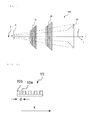
- FIG. 1 is a diagram illustrating a schematic structure of an X-ray Talbot interferometer 100 according to the embodiment of the present invention.
- the X-ray Talbot interferometer 100 includes an X-ray source 2, a first diffraction grating 10, a second diffraction grating 20, and an X-ray image detector 30.
- the first diffraction grating 10 and the second diffraction grating 20 are disposed in parallel with a predetermined distance therebetween in a z direction.
- the X-ray source 2 is disposed to be opposed to the first diffraction grating 10 along the z direction.
- the X-ray image detector 30 is disposed to be opposed to the second diffraction grating 20 along the z direction. Further, a sample 4 to be observed is disposed between the first diffraction grating 10 and the X-ray source 2 along the z direction.
- the first diffraction grating 10 and the second diffraction grating 20 have a plurality of groove portions 10a and 20a that are formed to extend along one direction parallel to a plane thereof (y direction in FIG. 1 ) and be spaced apart from one another in a predetermined period (see the cross section of the groove portions of FIGS. 2A and 2B ).
- the groove portions 10a and 20a transmit the X-ray, while a strip-like ridge portion 10b between the neighboring groove portions 10a transmits the X-ray after shifting the phase by ⁇ /2, and a ridge portion 20b blocks (absorbs) the X-ray.
- the groove portions 10a and 20a, and the ridge portions 10b and 20b extend in the Y direction of FIG.
- a width (interval) of the ridge portion 10b and a width (interval) of the groove portion 10a are the same, and a width (interval) of the ridge portion 20b and a width (interval) of the groove portion 20a are the same.
- the X-ray Talbot interferometer 100 when the X-ray is irradiated from the X-ray source 2 to the first diffraction grating 10 via the sample 4, the X-ray transmitted through the groove portion 10a interferes with the X-ray transmitted and diffracted through the ridge portion 10b. Then, the self image having the same pattern as that immediately after transmission is formed at a position separated by the Talbot distance.
- the first diffraction grating 10 constitutes the phase diffraction grating that performs phase modulation on the irradiated X-ray.
- the second diffraction grating 20 disposed to the rear of the first diffraction grating 10 diffracts the X-ray diffracted by the first diffraction grating 10 so as to form an image contrast
- the X-ray image detector 30 disposed to the rear of the second diffraction grating 20 detects the diffracted X-ray.
- the groove portion 20a of the second diffraction grating 20 have a high X-ray transmittance and the ridge portion 20b have a low X-ray transmittance. Therefore, it is preferred that the second diffraction grating 20 be an amplitude diffraction grating having a larger thickness than the first diffraction grating 10.
- the sample 4 is disposed in front of the first diffraction grating 10 and the irradiated X-ray passes through the sample 4 in a slightly different light path, and hence a manner of an interference pattern varies in accordance with the phase difference at this time. Therefore, the self image is deformed.
- a moire fringe is generated in a Talbot interference image (image contrast), which is detected by the X-ray image detector 30.
- An amount of modulation of the generated moire fringe by the sample 4 is proportional to an angle of bending of the irradiated X-ray by the sample 4. Therefore, through analysis of the moire fringe, the sample 4 and an internal structure thereof can be measured.
- a fringe scan method as one of analyzing methods of the moire fringe focuses attention on the fact that a phase of the moire fringe is changed by shifting the first diffraction grating 10 and the second diffraction grating 20 relatively in the X direction.
- the phase of the moire fringe is changed so as to obtain a plurality of Talbot interference images, and then the plurality of Talbot interference images are combined by an integral process.
- the phase image (the sample 4 and the internal structure thereof) can be obtained.
- CT image tomographic image
- the X-ray Talbot interferometer 100 of the present invention includes a Talbot-Lau interferometer in which a multi-slit is disposed between the X-ray source 2 and the sample 4.
- a multi-slit is disposed between the X-ray source 2 and the sample 4.
- a microfocus X-ray source is necessary to use a microfocus X-ray source as the X-ray source 2.
- a usual X-ray source can be used in the Talbot-Lau interferometer.
- the X-ray has a short wavelength, and hence, in order to secure coherency, the thickness of the ridge portion of the first diffraction grating 10 and the second diffraction grating 20 is required to be approximately 10 ⁇ m or smaller. Further, in the phase diffraction grating, the contrast of the self image becomes highest when a phase shift amount becomes ⁇ /2. Therefore, in order to realize this, it is necessary to set the thickness of the ridge portion (depth of the groove) at approximately 1 to 10 ⁇ m, and fine machining and manufacturing techniques are required. For instance, when the ridge portion of each diffraction grating is formed of gold, it is necessary to set the thickness of the ridge portion to approximately 1 to 3 ⁇ m. When the ridge portion is formed of copper, it is necessary to set the thickness of the ridge portion to approximately 3 to 10 ⁇ m.
- the amplitude diffraction grating in order to function as the amplitude diffraction grating, it is necessary to set a high X-ray transmittance of the groove portion of the diffraction grating and to set a low X-ray transmittance of the ridge portion. Therefore, it is required to set the thickness of the ridge portion (depth of the groove) to a large value of approximately 10 to 100 ⁇ m even when gold is used. Therefore, the aspect ratio expressed by (depth of groove)/(width of groove) of the diffraction grating becomes quite as large as three or larger (ten or larger in some cases).
- a fine X-ray absorbing portion (groove portion) having the side wall with a sharp shape can be formed by cutting a metal film using, for example, a monocrystal diamond cutting tool that has a high hardness and enables precise machining of the groove.
- FIG. 3 illustrates a structure of the diffraction grating 20 for the X-ray Talbot interferometer according to the embodiment of the present invention.
- the diffraction grating 20 for the X-ray Talbot interferometer is the second diffraction grating (amplitude diffraction grating) 20 described above with reference to FIG. 1 , and the aspect ratio expressed by (depth of groove)/(width of groove) is preferably three or higher.
- the present invention can be applied also to the first diffraction grating 10 as the phase diffraction grating, but is preferably applied at least to the above-mentioned amplitude diffraction grating having a high aspect ratio.
- the diffraction grating 20 for the X-ray Talbot interferometer includes a substrate 22, a plurality of ridge-like X-ray absorbing portions 20b which are made of a metal and formed on the substrate 22 along one direction at predetermined intervals, and a resin 26 interposed in the groove portion 20a between the neighboring X-ray absorbing portions.
- the X-ray absorbing portion 20b is formed by cutting a metal film (described later). It is preferred that a roughness of a side wall 20s of the X-ray absorbing portion 20b and a curvature radius of a cut corner portion formed by the side wall 20s and the bottom of the groove portion be 0.1 ⁇ m or smaller each.
- the roughness of the side wall 20s has an arithmetical mean height Ra of 0.1 ⁇ m or smaller, as defined in JIS B0601.
- the plurality of ridge-like X-ray absorbing portions 20b contain gold as a main component and are formed of one of crystals each having an average grain diameter of 0.1 ⁇ m or smaller and amorphous gold.
- the roughness of the side wall, squareness, and straightness mostly depend on a shape of the cutting tool. Accuracy of a moving mechanism of a superfine nano machine described later is higher than roughness of the surface of the cutting tool.
- an intermediate layer 24 is interposed between the X-ray absorbing portion 20b and the substrate 22.
- the substrate 22 be made of a material having at least one main component selected from the group consisting of carbon, silicon, and aluminum, for example, in order to increase the X-ray transmittance.
- a material having at least one main component selected from the group consisting of carbon, silicon, and aluminum for example, in order to increase the X-ray transmittance.
- composition of the substrate 22 there is an amorphous carbon wafer or a silicon wafer, a silicon nitride membrane or a silicon carbide membrane, a 3000-series aluminum sheet, an aluminum-magnesium alloy sheet, or the like, for example.
- the X-ray transmittance can be enhanced so that a good diffraction characteristic can be obtained.
- the X-ray absorption and phase shift amounts depend on a thickness of the metal film, and hence it is preferred that a cutting residue of the metal film does not exist in the bottom of the groove portion.
- the cutting tool is moved only in the direction along the groove in one groove cutting operation, and a constant direction of the depth of the groove is maintained so that the machining can be performed at high speed.
- the substrate including the metal film and the intermediate layer be flat.
- the flatness of the substrate including the metal film and the intermediate layer is set to be preferably 10 ⁇ m or smaller, and further the intermediate layer is formed into a thickness equal to or larger than this flatness.
- the intermediate layer 24 contains an element having a lower hardness (Vickers' hardness) than that of the substrate and a smaller effective atomic number than that of the metal film (the metal film serving as the X-ray absorbing portion 20b).
- This element may be a light element that is soft and easily transmits the X-ray, such as a metal (for example, aluminum).
- the intermediate layer 24 may be a resin.
- the intermediate layer 24 prevents the cutting tool from cutting the substrate 22 through excessive cutting when the metal film on the substrate 22 is cut so as to form the X-ray absorbing portion 20b.
- the substrate 22 is usually harder than the metal film, and hence the cutting tool is worn out by cutting the substrate 22.
- the metal film can be securely cut by an amount corresponding to the thickness thereof to form the deep groove portion.
- a part of the intermediate layer 24 softer than the substrate 22 is cut to prevent the cutting tool from being worn out.
- the intermediate layer itself has small X-ray absorption and phase change, and hence there is no problem even in a case where a part of the intermediate layer 24 is cut when forming the X-ray absorbing portion 20b.
- the intermediate layer 24 may be an aluminum layer or a multilayer film including an aluminum layer. However, the intermediate layer 24 is not an essential structure.
- the X-ray absorbing portion 20b can be formed by cutting a metal film containing gold as a main component, for example, a pure gold plating film, or a film of gold-nickel alloy plating or gold-nickel-tungsten alloy plating containing 90% or higher weight ratio of gold, which efficiently absorbs the X-ray so that a characteristic of the diffraction grating is improved.
- the metal film includes not only a pure metal but also an alloy as described above.
- the resin 26 is filled in the groove after the groove portion is formed so as to hold the X-ray absorbing portion 20b and prevent the X-ray absorbing portion 20b from being inclined or deformed.
- para-xylene polymer there is a polymer in which a part or a whole of hydrogen of the benzene ring of the para-xylene polymer or para-xylene is substituted with chlorine, or a polymer in which ⁇ -hydrogen atoms of para-xylene are substituted with fluorine, and parylene N, parylene C, parylene D, and parylene HT (all of which are registered trademarks) are commercially available.
- the cutting tool which has a cutting blade made of monocrystal diamond and is suitable for cutting the metal film to form the X-ray absorbing portion 20b, is described.
- the monocrystal diamond has high hardness and enables precise machining of the groove.
- FIG. 4 illustrates a tool main body (cutter) 400 to which a monocrystal diamond cutting tool 200 is mounted.
- the monocrystal diamond cutting tool 200 is mounted to a tip of a base metal 300 having a substantially trapezoidal shape so as to constitute the tool main body 400.
- the cutting blade of the monocrystal diamond cutting tool 200 protrudes from the tip of the base metal 300.
- the tool main body 400 is fixed to a holder of the cutting machine (not shown), and the monocrystal diamond cutting tool 200 can cut an object to be cut to form the groove therein as described later.
- the monocrystal diamond cutting tool 200 has a rake surface 201, two first flanks 203 and 204 that are side surfaces each adjacent to the rake surface 201, a front flank 205 that is adjacent to the rake surface 201 and is opposed to a cutting surface of an object to be cut, a front cutting blade 210 formed at a boundary between the rake surface 201 and the front flank 205, and two first cutting blades 213 and 214 formed at a boundary between the rake surface 201 and the first flank 203 and between the rake surface 201 and the first flank 204.
- Shapes of the front flank 205 and the rake surface 201 are not limited, and the shapes may be a flat surface or a curved surface.
- the rake surface 201 has a predetermined rake angle of zero degrees or a rake angle slightly inclined in a positive direction so as to scoop cutting waste.
- the first flank 203, 204 or the front flank 205 is formed by etching with a focused ion beam (FIB).
- FIB focused ion beam
- the etching with the FIB enables machining of a complicated shape, and has an advantage that any crystal surface can be machined. Therefore, even a (111) plane of diamond that is the hardest crystal plane can be easily machined. In contrast, in a case of polishing with a grindstone, for example, the (111) plane of diamond cannot be polished.
- a width W1 of the front cutting blade 210 it is preferred to set a width W1 of the front cutting blade 210 to 4 ⁇ m or smaller because a fine groove portion suitable for the diffraction grating for the X-ray Talbot interferometer can be formed.
- FIG. 6 is a plan view of the monocrystal diamond cutting tool 200 viewed from the point A of FIG. 5 .
- An interval W2 between the first flanks 203 and 204 is equal to or smaller than the width W1 of the front cutting blade 210.
- a part satisfying W2 ⁇ W1 constitutes the first flanks 203 and 204, and a width of a part on a rear end side of the first flanks 203 and 204 (part opposite to the front cutting blade 210) is larger than W2 so as to secure the strength.
- a contact area between the monocrystal diamond cutting tool 200 and the object to be cut is reduced in the cutting process, and hence the tool is less liable to chatter vibration so that precise cutting process can be performed.
- a length L of the first flanks 203 and 204 from the front cutting blade 210 is set three times or more as large as the width W1 of the front cutting blade and the deep groove is formed through cutting, when W2 ⁇ W1 is satisfied, the effect of reducing the contact area (friction) with the object to be cut is increased.
- the part extending in parallel at the width W1 from the front cutting blade 210 toward the rear end constitutes the first cutting blades 213 and 214, and the first cutting blades 213 and 214 are formed only in the vicinity of the front cutting blade 210.
- the monocrystal diamond cutting tool 200 (tool main body 400) described above is mounted to the cutting machine, and can form the groove portion 20a as illustrated in FIG. 7 .
- the period and the depth of the groove portions formed through cutting depend on a resolution of the superfine nano machine, and hence it is preferred to use the superfine nano machine having a nanometer-level resolution as the cutting machine.
- the superfine nano machine FANUC ROBONANO ⁇ -0iB manufactured by FANUC CORPORATION, for example, is commercially available.
- This superfine nano machine has a resolution of 1 nm in a linear axis by controlling a linear motor and a synchronous built-in servomotor so that five axes are directly driven simultaneously with high accuracy.
- the monocrystal diamond cutting tool 200 performs a drag cutting process on a metal film 20x along one direction (an arrow direction in FIG. 7 ) leaving the ridges having a predetermined width W3 in the direction perpendicular to the one direction.
- the metal film 20x is cut to form the groove portions 20a, and the ridge-like X-ray absorbing portion 20b can be formed between the neighboring groove portions 20a.
- W1 W3 be satisfied.
- the monocrystal diamond cutting tool 200 cuts the metal film 20x to form the groove portion 20a, and hence it is possible to perform appropriate machining, in which the roughness of side surfaces of the groove portion and the curvature radius of the cut corner portion formed by the side surface and the bottom surface of the groove portion are 0.1 ⁇ m or smaller each.
- electroforming is performed in the fine groove (slit) formed using a resist resin to manufacture the diffraction grating, a high precision diffraction grating can be obtained.
- the width of the groove portion 20a is the same as the width W1 of the front cutting blade 210, and a depth L of the groove portion 20a to be formed through cutting is up to a vertical length of the first flanks 203 and 204.
- the second diffraction grating (amplitude diffraction grating) illustrated in FIG. 1 it is necessary to set the aspect ratio expressed by (depth of groove)/(width of groove) to a high value (for example, three or higher). Therefore, with use of the monocrystal diamond cutting tool having high hardness, even when the cutting tool is elongated so that L/W1 becomes three or larger, the metal film can be cut sufficiently deeply.
- the monocrystal diamond cutting tool satisfying W2 ⁇ W1 is used as described above, the contact area (friction) with the object to be cut is reduced so that the groove portion 20a having a high aspect ratio can be securely formed through cutting.
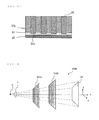
- the intermediate layer 24 is formed on the silicon wafer substrate 22 as necessary, and then a metal film 20bx is formed on the intermediate layer 24 ( FIG. 8A ; metal film forming step).
- a metal film 20bx is formed on the intermediate layer 24 ( FIG. 8A ; metal film forming step).
- an aluminum film is formed by ion plating or sputtering vapor deposition.
- electric copper plating is used.
- a thin chromium vapor deposition film may be formed between the substrate 22 and the intermediate layer 24 for securing adhesiveness of the intermediate layer.
- the metal film 20bx a gold film is formed by electric plating. In order to secure adhesiveness of the metal film 20bx, it is possible to form a thin gold film on the surface of the intermediate layer 24 by vapor deposition, and then to perform electric plating of gold.
- the metal film 20bx is cut along one direction (direction perpendicular to the drawing sheet of FIGS. 8A to 8D ) at predetermined intervals so that the plurality of groove portions 20a are formed, and the ridge-like X-ray absorbing portion 20b is formed between the neighboring groove portions 20a ( FIG. 8B ; cutting step).
- the cutting allowance in the cutting depth direction is set to approximately 0.3 to 1 ⁇ m, and the cutting is performed a plurality of times so that the groove portions 20a having a predetermined depth are formed.
- an uncured resin 26x is filled in the groove portion 20a ( FIG. 8C ; resin filling step).
- the uncured resin 26x fills the groove portion 20a and also covers the surface of the X-ray absorbing portion 20b.
- polyimide and a para-xylene polymer it is preferred to use at least one or both of polyimide and a para-xylene polymer as the uncured resin 26x.
- polyimide it is preferred to fill polyimide in the groove portion 20a by the vacuum injection method because polyimide can flow into a deep portion of the groove portion 20a.
- para-xylene polymer it is preferred to fill the para-xylene polymer in the groove portion 20a by the vacuum vapor deposition method because the para-xylene polymer can be deposited in the deep portion of the groove portion 20a.
- the vacuum injection method is a method in which the substrate 22 having the groove portions 20a is disposed in a system maintained in vacuum, and low molecular weight polyimide is supplied to the system to flow into the groove portion 20a and then is polymerized by ultraviolet rays or heat to cause a crosslinking reaction.
- a dimer of para-xylene is heated to approximately 175°C to evaporate in the vacuum. After that, the vapor of the para-xylene dimer is heated to approximately 680°C to be thermally decomposed substances.
- the thermally decomposed substances of para-xylene reaches the surface of the groove portion 20a or the X-ray absorbing portion 20b, the thermally decomposed substances are reacted with each other into a stable vapor deposition film.
- the surface of the polymerized and cured resin 26x is ground or ashed so that the upper surface of the X-ray absorbing portion 20b is exposed to be flushed with the resin 26 ( FIG. 8D ).
- a fine grindstone is moved to slide in the same direction as cutting of the groove 20a so that the resin pushed out from the upper part is ground off.
- the ashing can be performed by using a known ashing apparatus (technique) used in semiconductor technology, and for example, photo excited ashing and plasma ashing can be used.
Landscapes
- Physics & Mathematics (AREA)
- Spectroscopy & Molecular Physics (AREA)
- Engineering & Computer Science (AREA)
- General Engineering & Computer Science (AREA)
- High Energy & Nuclear Physics (AREA)
- Measurement Of Radiation (AREA)
- Analysing Materials By The Use Of Radiation (AREA)
- Diffracting Gratings Or Hologram Optical Elements (AREA)
Abstract
Description
- The present invention relates to a diffraction grating for an X-ray Talbot interferometer, a method of manufacturing the same, and an X-ray Talbot interferometer.
- There is known a Talbot effect, in which a diffraction grating is used and self images of the diffraction grating are formed at specific distances from the diffraction grating when light from a coherent light source passes through the diffraction grating. In recent years, there has been developed an X-ray Talbot interferometer that uses this Talbot effect so as to detect a phase shift of a transmitted X-ray. An image obtained by the phase shift of an X-ray using the Talbot effect is advantageous in having higher contrast particularly in a substance having a small atomic number than a conventional image obtained by an absorbed amount of a transmitted X-ray.
- As such an X-ray Talbot interferometer, there is known a structure illustrated in
FIG. 9 . The X-ray Talbotinterferometer 1000 includes afirst diffraction grating 1010, a second diffraction grating 1020, and an X-ray image detector 30 (see International PatentWO 2004/58070 A FIGS. 10A and 10B , the first diffraction grating 1010 and the second diffraction grating 1020 havegrooves ridge portion 1010b between neighboring grooves transmits the X-ray after shifting the phase by π/2, and aridge portion 1020b blocks (absorbs) the X-ray. As a material of the diffraction grating, gold (Au) having high X-ray absorbing power is usually used. - In this X-ray Talbot interferometer, when the X-ray is irradiated from an X-ray source to the first diffraction grating via a sample, the X-ray transmitted through the
groove portion 1010a and the X-ray transmitted and diffracted through theridge portion 1010b interfere with each other. Then, self images of thefirst diffraction grating 1010 are formed at positions of integral multiples of a Talbot distance d2/2λ of the first diffraction grating 1010 (d represents a period of the diffraction grating, and λ represents a wavelength of the X-ray) as the Talbot effect. The self image has a distortion due to asample 4, and the distortion has information of the sample. The second diffraction grating 1020 is disposed at a position where the self image of thefirst diffraction grating 1010 is formed. Then, a distribution of the X-ray transmitted through the second diffraction grating 1020 has moire fringes because the first self image is overlaid. Therefore, this X-ray distribution is detected by the X-ray image detector, and image analysis is performed so that an image of thesample 4 is obtained. In order to improve image contrast, it is preferred that thegroove portion 1020a of the second diffraction grating 1020 have a high X-ray transmittance, while theridge portion 1020b have a low X-ray transmittance. Therefore, it is preferred that the second diffraction grating 1020 be an amplitude diffraction grating having a larger thickness than thefirst diffraction grating 1010. - Here, in order to generate the Talbot effect, it is necessary that the ridge portions (X-ray absorbing portions) of the diffraction grating have a period securing coherency of the X-ray. Therefore, the thickness of the ridge portion is required to be approximately 10 µm or smaller. Further, in a phase diffraction grating, the contrast of the self image becomes highest when a phase shift amount becomes π/2. Therefore, in order to realize this, it is necessary to set a thickness of the ridge portion (depth of the groove) at approximately 1 to 10 µm, and fine machining and manufacturing technique are required.
- On the other hand, in order to function as the amplitude diffraction grating, it is preferred that the
groove portion 1020a of the diffraction grating have a high X-ray transmittance and theridge portion 1020b have a low X-ray transmittance. Therefore, it is required to form the groove to have a large depth of approximately 10 to 100 µm even when gold is used. Therefore, an aspect ratio expressed by (depth of groove)/(width of groove) of the diffraction grating becomes very large, and hence production of the diffraction grating becomes difficult. - Therefore, there is disclosed a technique of manufacturing the diffraction grating for the X-ray Talbot interferometer, in which a deep groove is formed in a resin by X-ray lithography using an X-ray mask, and the X-ray absorbing portion is formed in the groove by an electroforming method (see Japanese Patent Application Laid-open No.
2006-259264 - In addition, there is disclosed a technique including the steps of patterning and removing a photosensitive resin on a surface of a silicon substrate by a lithography method, etching the silicon substrate, from which the photosensitive resin is removed, by an ICP plasma etching method so as to form a slit groove, then depositing an insulator material in the slit groove, further etching the remaining photosensitive resin and the silicon substrate by the ICP plasma etching method so as to form a second slit groove, and forming an X-ray absorbing metal portion in the second slit groove by the electroforming method (see Japanese Patent Application Laid-open No.
2009-42528 - However, in the technique described in Japanese Patent Application Laid-open No.
2006-259264 2009-42528 - Therefore, an object of the present invention is to provide a diffraction grating for an X-ray Talbot interferometer, a method of manufacturing the same, and an X-ray Talbot interferometer, the method enabling easy and highly accurate manufacturing of a diffraction grating having grooves with a high aspect ratio.
- A diffraction grating for an X-ray Talbot interferometer according to an exemplary embodiment of the present invention includes a plurality of ridge-like X-ray absorbing portions formed on a substrate along one direction at predetermined intervals through cutting of a metal film.
- The period and the depth of the groove portions formed on the substrate in this way depend on resolution and stability of a cutting machine. Therefore, when a superfine nano machine that can realize a nanometer-level machining resolution and stability is used, diffraction performance of the X-ray diffraction grating is improved. In addition, the superfine nano machine is less expensive than a facility used in the X-ray lithography and is not required to use the X-ray mask, and hence manufacturing cost of the X-ray diffraction grating can be reduced.
- In addition, a roughness of a side wall of the groove portion formed in the cutting process and a radius of a round corner formed by the side wall and the bottom surface of the groove portion (hereinafter referred to as "curvature radius of a cut corner portion") depend on a shape of a cutting tool used for cutting. If a monocrystal diamond cutting tool is used, a roughness and a round corner radius (curvature radius)of the cutting blade can be 0.1 µm or smaller. As a result, diffraction performance of the X-ray diffraction grating can be improved.
- Further, the aspect ratio expressed by (depth of groove)/(width of groove) is preferably three or larger. When the monocrystal diamond cutting tool having high hardness is used for machining, the X-ray diffraction grating having a high aspect ratio can be manufactured.
- Note that, conventionally, the ridge is formed of a resist as a soft insulator, and then the X-ray absorbing portion is formed by electroforming. Therefore, it is difficult to form the X-ray absorbing portion precisely because the resist may be inclined or come into contact with each other. However, in the present invention, the ridge portion serving as the X-ray absorbing portion is formed by machining a metal as a conductor having a higher Young's modulus than that of the resist by one order of magnitude. Therefore, it is possible to form the X-ray absorbing portion precisely.
- It is preferred that a width of each of the plurality of ridge-like X-ray absorbing portions be the same as a width of each of groove portions, and the width of the each of the plurality of ridge-like X-ray absorbing portions and the width of the each of the groove portions be 4 µm or smaller.
- The X-ray has a short wavelength and a small diffraction angle, and hence, in order to obtain effective interference, it is necessary to set a large distance between the X-ray source and the grating, a small period of the diffraction grating, and low energy of the X-ray so that the wavelength becomes long. When each of the groove portion and the ridge portion has a width of 4 µm or smaller, an effective interference image can be obtained at a practical distance between the X-ray source and the grating (3 m or smaller) and practical X-ray energy (10 to 40 keV). In addition, when the groove portion and the ridge portion have the same width, a phase image has the highest sharpness.
- When a resin is interposed in a groove portion between neighboring X-ray absorbing portions of the plurality of ridge-like X-ray absorbing portions, the X-ray absorbing portions are not inclined or do not come into contact with each other.
- According to an exemplary embodiment of the present invention, there is provided a method of manufacturing a diffraction grating for an X-ray Talbot interferometer, the method including: forming a metal film on a substrate; and cutting the metal film along one direction in a predetermined period so as to form a plurality of groove portions, to thereby form a ridge-like metal layer between neighboring groove portions of the plurality of groove portions.
- It is preferred that a material to be used for the substrate include at least one element of carbon, silicon, and aluminum as a main component.
- With the use of the above-mentioned material for the substrate, the X-ray transmittance can be enhanced so that a diffraction characteristic can be improved.
- It is preferred that the method further include forming an intermediate layer between the substrate and the metal film, the intermediate layer having a smaller hardness than the substrate and containing an element having a smaller effective atomic number than an element contained in the metal film.
- The substrate is usually harder than the metal film, and hence the cutting tool is worn out when cutting the substrate. However, with the formation of the intermediate layer between the metal film and the substrate, the metal film can be securely cut by an amount corresponding to the thickness thereof so that a deep groove portion can be formed. In addition, through cutting a part of the intermediate layer that is softer than the substrate, it is possible to prevent the cutting tool from being worn out.
- In addition, the X-ray absorption and phase shift amounts depend on a thickness of the metal film, and hence it is preferred that a cutting residue of the metal film do not exist in the bottom of the groove portion. Here, as to a movement of the cutting machine when machining a large number of grooves, the cutting tool is moved only in the direction along the groove in one groove cutting, and a constant direction of the depth of the groove is maintained so that the machining can be performed at high speed. In this case, in order to eliminate the cutting residue of the metal film, it is preferred that the substrate including the metal film and the intermediate layer be flat. However, each film thickness and unevenness of the substrate when the substrate is mounted to the cutting machine have a variation of a few microns or smaller each. Therefore, the flatness of the substrate including the metal film and the intermediate layer is set to be preferably 10 µm or smaller, and further the intermediate layer is formed into a thickness equal to or larger than this flatness. Thus, the cutting residue of the metal film does not remain, and it is possible to prevent the cutting tool from being worn out by cutting the substrate. As the hardness, Vickers' hardness can be adopted.
- It is preferred that the resin include at least one of polyimide and a para-xylene polymer because such a resin is superior in mechanical strength and has high durability with respect to an X-ray, particularly in phase imaging.
- It is preferred to fill the resin containing polyimide in the each of the plurality of groove portions by a vacuum injection method because polyimide can flow into a deep portion of the groove portion.
- It is preferred to fill the para-xylene polymer in the each of the plurality of groove portions by a vacuum vapor deposition method because the para-xylene polymer can flow into the deep portion of the groove portion.
- In the above-mentioned cutting, it is preferred to use a cutting tool having a cutting blade made of monocrystal diamond because monocrystal diamond has high hardness and enables precise machining of the groove.
- An X-ray Talbot interferometer according to an exemplary embodiment of the present invention uses the above-mentioned diffraction grating for an X-ray Talbot interferometer.
- According to the present invention, the diffraction grating for an X-ray Talbot interferometer having grooves with a high aspect ratio can be manufactured easily with high accuracy.
- Embodiments of the present invention will now be described by way of further example only and with reference to the accompanying drawings, in which:
-
FIG. 1 is a diagram illustrating a schematic structure of an X-ray Talbot interferometer according to an embodiment of the present invention; -
FIGS. 2A and2B illustrate cross sections of a first diffraction grating and a second diffraction grating, which are taken along an x direction; -
FIG. 3 is a perspective view illustrating a structure of a diffraction grating for the X-ray Talbot interferometer according to the embodiment of the present invention; -
FIG. 4 is a perspective view illustrating a tool main body to which a monocrystal diamond cutting tool is mounted; -
FIG. 5 is a perspective view illustrating the monocrystal diamond cutting tool; -
FIG. 6 is a plan view of the monocrystal diamond cutting tool viewed from the point A ofFIG. 5 ; -
FIG. 7 is a diagram illustrating a method of forming each unit metal layer using the monocrystal diamond cutting tool; -
FIGS. 8A to 8D are a process charts illustrating an example of a method of manufacturing the diffraction grating for the X-ray Talbot interferometer; -
FIG. 9 is a diagram illustrating a schematic structure of a conventional X-ray Talbot interferometer; and -
FIGS. 10A and 10B illustrate cross sections of a first diffraction grating and a second diffraction grating of a conventional X-ray Talbot interferometer, which are taken along an x direction. - Hereinafter, an embodiment of the present invention is described.
FIG. 1 is a diagram illustrating a schematic structure of anX-ray Talbot interferometer 100 according to the embodiment of the present invention. TheX-ray Talbot interferometer 100 includes anX-ray source 2, afirst diffraction grating 10, asecond diffraction grating 20, and anX-ray image detector 30. Thefirst diffraction grating 10 and thesecond diffraction grating 20 are disposed in parallel with a predetermined distance therebetween in a z direction. TheX-ray source 2 is disposed to be opposed to thefirst diffraction grating 10 along the z direction. In addition, theX-ray image detector 30 is disposed to be opposed to thesecond diffraction grating 20 along the z direction. Further, asample 4 to be observed is disposed between thefirst diffraction grating 10 and theX-ray source 2 along the z direction. - The
first diffraction grating 10 and thesecond diffraction grating 20 have a plurality ofgroove portions FIG. 1 ) and be spaced apart from one another in a predetermined period (see the cross section of the groove portions ofFIGS. 2A and2B ). Thegroove portions like ridge portion 10b between the neighboringgroove portions 10a transmits the X-ray after shifting the phase by π/2, and aridge portion 20b blocks (absorbs) the X-ray. Thegroove portions ridge portions FIG. 1 . As a material of the diffraction grating, it is preferred to use gold having high X-ray absorbing power. Note that, in this embodiment, a width (interval) of theridge portion 10b and a width (interval) of thegroove portion 10a are the same, and a width (interval) of theridge portion 20b and a width (interval) of thegroove portion 20a are the same. - In the
X-ray Talbot interferometer 100, when the X-ray is irradiated from theX-ray source 2 to thefirst diffraction grating 10 via thesample 4, the X-ray transmitted through thegroove portion 10a interferes with the X-ray transmitted and diffracted through theridge portion 10b. Then, the self image having the same pattern as that immediately after transmission is formed at a position separated by the Talbot distance. In other words, thefirst diffraction grating 10 constitutes the phase diffraction grating that performs phase modulation on the irradiated X-ray. Here, in order to generate the Talbot effect, it is necessary to adjust the period d of the ridge portion (X-ray absorbing portion) of the first diffraction grating 10 (seeFIG. 2A ) so as to secure coherency of the X-ray irradiated from theX-ray source 2. - In addition, the
second diffraction grating 20 disposed to the rear of the first diffraction grating 10 (position of the self image) diffracts the X-ray diffracted by thefirst diffraction grating 10 so as to form an image contrast, and theX-ray image detector 30 disposed to the rear of thesecond diffraction grating 20 detects the diffracted X-ray. In order to improve the image contrast, it is preferred that thegroove portion 20a of thesecond diffraction grating 20 have a high X-ray transmittance and theridge portion 20b have a low X-ray transmittance. Therefore, it is preferred that thesecond diffraction grating 20 be an amplitude diffraction grating having a larger thickness than thefirst diffraction grating 10. - Here, the
sample 4 is disposed in front of thefirst diffraction grating 10 and the irradiated X-ray passes through thesample 4 in a slightly different light path, and hence a manner of an interference pattern varies in accordance with the phase difference at this time. Therefore, the self image is deformed. When thesecond diffraction grating 20 is overlaid at a position of the self image, a moire fringe is generated in a Talbot interference image (image contrast), which is detected by theX-ray image detector 30. An amount of modulation of the generated moire fringe by thesample 4 is proportional to an angle of bending of the irradiated X-ray by thesample 4. Therefore, through analysis of the moire fringe, thesample 4 and an internal structure thereof can be measured. - Note that, a fringe scan method as one of analyzing methods of the moire fringe focuses attention on the fact that a phase of the moire fringe is changed by shifting the
first diffraction grating 10 and thesecond diffraction grating 20 relatively in the X direction. In other words, the phase of the moire fringe is changed so as to obtain a plurality of Talbot interference images, and then the plurality of Talbot interference images are combined by an integral process. Thus, the phase image (thesample 4 and the internal structure thereof) can be obtained. - In addition, it is also possible to obtain a tomographic image (CT image) of the
sample 4 by rotating thesample 4 so as to obtain differential phase images from many irradiation directions, and by combining the differential phase images by the integral process or the like. - Note that, the
X-ray Talbot interferometer 100 of the present invention includes a Talbot-Lau interferometer in which a multi-slit is disposed between theX-ray source 2 and thesample 4. When the multi-slit is not used, it is necessary to use a microfocus X-ray source as theX-ray source 2. In contrast, a usual X-ray source can be used in the Talbot-Lau interferometer. - The X-ray has a short wavelength, and hence, in order to secure coherency, the thickness of the ridge portion of the
first diffraction grating 10 and thesecond diffraction grating 20 is required to be approximately 10 µm or smaller. Further, in the phase diffraction grating, the contrast of the self image becomes highest when a phase shift amount becomes π/2. Therefore, in order to realize this, it is necessary to set the thickness of the ridge portion (depth of the groove) at approximately 1 to 10 µm, and fine machining and manufacturing techniques are required. For instance, when the ridge portion of each diffraction grating is formed of gold, it is necessary to set the thickness of the ridge portion to approximately 1 to 3 µm. When the ridge portion is formed of copper, it is necessary to set the thickness of the ridge portion to approximately 3 to 10 µm. - On the other hand, in order to function as the amplitude diffraction grating, it is necessary to set a high X-ray transmittance of the groove portion of the diffraction grating and to set a low X-ray transmittance of the ridge portion. Therefore, it is required to set the thickness of the ridge portion (depth of the groove) to a large value of approximately 10 to 100 µm even when gold is used. Therefore, the aspect ratio expressed by (depth of groove)/(width of groove) of the diffraction grating becomes quite as large as three or larger (ten or larger in some cases).
- For this reason, it is necessary to form the X-ray absorbing portion (ridge portion) finely and to form a shape of the side wall thereof to be sharp (in other words, clearly defined such that a roughness of the side wall of the groove and a radius of a round corner formed by the side wall and the bottom surface (curvature radius of a cut corner portion) are fine). The inventors of the present invention found that a fine X-ray absorbing portion (groove portion) having the side wall with a sharp shape can be formed by cutting a metal film using, for example, a monocrystal diamond cutting tool that has a high hardness and enables precise machining of the groove.
-
FIG. 3 illustrates a structure of thediffraction grating 20 for the X-ray Talbot interferometer according to the embodiment of the present invention. Thediffraction grating 20 for the X-ray Talbot interferometer is the second diffraction grating (amplitude diffraction grating) 20 described above with reference toFIG. 1 , and the aspect ratio expressed by (depth of groove)/(width of groove) is preferably three or higher. Note that, the present invention can be applied also to thefirst diffraction grating 10 as the phase diffraction grating, but is preferably applied at least to the above-mentioned amplitude diffraction grating having a high aspect ratio. - The
diffraction grating 20 for the X-ray Talbot interferometer includes asubstrate 22, a plurality of ridge-likeX-ray absorbing portions 20b which are made of a metal and formed on thesubstrate 22 along one direction at predetermined intervals, and aresin 26 interposed in thegroove portion 20a between the neighboring X-ray absorbing portions. TheX-ray absorbing portion 20b is formed by cutting a metal film (described later). It is preferred that a roughness of aside wall 20s of theX-ray absorbing portion 20b and a curvature radius of a cut corner portion formed by theside wall 20s and the bottom of the groove portion be 0.1 µm or smaller each. Preferably, the roughness of theside wall 20s has an arithmetical mean height Ra of 0.1 µm or smaller, as defined in JIS B0601. Preferably, the plurality of ridge-likeX-ray absorbing portions 20b contain gold as a main component and are formed of one of crystals each having an average grain diameter of 0.1 µm or smaller and amorphous gold. Note that, the roughness of the side wall, squareness, and straightness mostly depend on a shape of the cutting tool. Accuracy of a moving mechanism of a superfine nano machine described later is higher than roughness of the surface of the cutting tool. - In addition, an
intermediate layer 24 is interposed between theX-ray absorbing portion 20b and thesubstrate 22. - It is preferred that the
substrate 22 be made of a material having at least one main component selected from the group consisting of carbon, silicon, and aluminum, for example, in order to increase the X-ray transmittance. As a specific example of composition of thesubstrate 22, there is an amorphous carbon wafer or a silicon wafer, a silicon nitride membrane or a silicon carbide membrane, a 3000-series aluminum sheet, an aluminum-magnesium alloy sheet, or the like, for example. - With the use of the above-mentioned material as the
substrate 22, the X-ray transmittance can be enhanced so that a good diffraction characteristic can be obtained. In addition, the X-ray absorption and phase shift amounts depend on a thickness of the metal film, and hence it is preferred that a cutting residue of the metal film does not exist in the bottom of the groove portion. Here, as to a movement of the cutting machine when machining a large number of grooves, the cutting tool is moved only in the direction along the groove in one groove cutting operation, and a constant direction of the depth of the groove is maintained so that the machining can be performed at high speed. In this case, in order to eliminate the cutting residue of the metal film, it is preferred that the substrate including the metal film and the intermediate layer be flat. However, both film thickness and unevenness of the substrate when the substrate is mounted to the cutting machine have a variation of a few microns or smaller each. Therefore, the flatness of the substrate including the metal film and the intermediate layer is set to be preferably 10 µm or smaller, and further the intermediate layer is formed into a thickness equal to or larger than this flatness. Thus, it is possible to prevent the cutting residue of the metal film from remaining, and to prevent the cutting tool from being worn out by cutting the substrate. - The
intermediate layer 24 contains an element having a lower hardness (Vickers' hardness) than that of the substrate and a smaller effective atomic number than that of the metal film (the metal film serving as theX-ray absorbing portion 20b). This element may be a light element that is soft and easily transmits the X-ray, such as a metal (for example, aluminum). Theintermediate layer 24 may be a resin. Theintermediate layer 24 prevents the cutting tool from cutting thesubstrate 22 through excessive cutting when the metal film on thesubstrate 22 is cut so as to form theX-ray absorbing portion 20b. Thesubstrate 22 is usually harder than the metal film, and hence the cutting tool is worn out by cutting thesubstrate 22. However, with the formation of theintermediate layer 24 between the metal film and thesubstrate 22, the metal film can be securely cut by an amount corresponding to the thickness thereof to form the deep groove portion. In addition, a part of theintermediate layer 24 softer than thesubstrate 22 is cut to prevent the cutting tool from being worn out. Note that, the intermediate layer itself has small X-ray absorption and phase change, and hence there is no problem even in a case where a part of theintermediate layer 24 is cut when forming theX-ray absorbing portion 20b. - The
intermediate layer 24 may be an aluminum layer or a multilayer film including an aluminum layer. However, theintermediate layer 24 is not an essential structure. - The
X-ray absorbing portion 20b can be formed by cutting a metal film containing gold as a main component, for example, a pure gold plating film, or a film of gold-nickel alloy plating or gold-nickel-tungsten alloy plating containing 90% or higher weight ratio of gold, which efficiently absorbs the X-ray so that a characteristic of the diffraction grating is improved. Note that, the metal film includes not only a pure metal but also an alloy as described above. - The
resin 26 is filled in the groove after the groove portion is formed so as to hold theX-ray absorbing portion 20b and prevent theX-ray absorbing portion 20b from being inclined or deformed. In particular, it is preferred to use at least one of polyimide and a para-xylene polymer as theresin 26 because such a material is superior in mechanical strength and has high durability with respect to an X-ray, particularly in phase imaging. As the para-xylene polymer, there is a polymer in which a part or a whole of hydrogen of the benzene ring of the para-xylene polymer or para-xylene is substituted with chlorine, or a polymer in which α-hydrogen atoms of para-xylene are substituted with fluorine, and parylene N, parylene C, parylene D, and parylene HT (all of which are registered trademarks) are commercially available. - Next, with reference to
FIGS. 4 to 7 , the cutting tool, which has a cutting blade made of monocrystal diamond and is suitable for cutting the metal film to form theX-ray absorbing portion 20b, is described. The monocrystal diamond has high hardness and enables precise machining of the groove. -
FIG. 4 illustrates a tool main body (cutter) 400 to which a monocrystaldiamond cutting tool 200 is mounted. The monocrystaldiamond cutting tool 200 is mounted to a tip of abase metal 300 having a substantially trapezoidal shape so as to constitute the toolmain body 400. The cutting blade of the monocrystal diamond cutting tool 200 (seeFIG. 5 ) protrudes from the tip of thebase metal 300. The toolmain body 400 is fixed to a holder of the cutting machine (not shown), and the monocrystaldiamond cutting tool 200 can cut an object to be cut to form the groove therein as described later. - As illustrated in
FIG. 5 , the monocrystaldiamond cutting tool 200 has arake surface 201, twofirst flanks rake surface 201, afront flank 205 that is adjacent to therake surface 201 and is opposed to a cutting surface of an object to be cut, afront cutting blade 210 formed at a boundary between therake surface 201 and thefront flank 205, and twofirst cutting blades rake surface 201 and thefirst flank 203 and between therake surface 201 and thefirst flank 204. Shapes of thefront flank 205 and therake surface 201 are not limited, and the shapes may be a flat surface or a curved surface. Therake surface 201 has a predetermined rake angle of zero degrees or a rake angle slightly inclined in a positive direction so as to scoop cutting waste. - The
first flank front flank 205 is formed by etching with a focused ion beam (FIB). The etching with the FIB enables machining of a complicated shape, and has an advantage that any crystal surface can be machined. Therefore, even a (111) plane of diamond that is the hardest crystal plane can be easily machined. In contrast, in a case of polishing with a grindstone, for example, the (111) plane of diamond cannot be polished. - It is preferred to set a width W1 of the
front cutting blade 210 to 4 µm or smaller because a fine groove portion suitable for the diffraction grating for the X-ray Talbot interferometer can be formed. -
FIG. 6 is a plan view of the monocrystaldiamond cutting tool 200 viewed from the point A ofFIG. 5 . An interval W2 between thefirst flanks front cutting blade 210. In other words, a part satisfying W2≤W1 constitutes thefirst flanks first flanks 203 and 204 (part opposite to the front cutting blade 210) is larger than W2 so as to secure the strength. In addition, if W2≤W1 is satisfied, a contact area between the monocrystaldiamond cutting tool 200 and the object to be cut is reduced in the cutting process, and hence the tool is less liable to chatter vibration so that precise cutting process can be performed. In particular, as illustrated inFIG. 6 , in case where a length L of thefirst flanks front cutting blade 210 is set three times or more as large as the width W1 of the front cutting blade and the deep groove is formed through cutting, when W2≤W1 is satisfied, the effect of reducing the contact area (friction) with the object to be cut is increased. - Note that, in this embodiment, the part extending in parallel at the width W1 from the
front cutting blade 210 toward the rear end constitutes thefirst cutting blades first cutting blades front cutting blade 210. - The monocrystal diamond cutting tool 200 (tool main body 400) described above is mounted to the cutting machine, and can form the
groove portion 20a as illustrated inFIG. 7 . Here, the period and the depth of the groove portions formed through cutting depend on a resolution of the superfine nano machine, and hence it is preferred to use the superfine nano machine having a nanometer-level resolution as the cutting machine. As the superfine nano machine, FANUC ROBONANO α-0iB manufactured by FANUC CORPORATION, for example, is commercially available. This superfine nano machine has a resolution of 1 nm in a linear axis by controlling a linear motor and a synchronous built-in servomotor so that five axes are directly driven simultaneously with high accuracy. - Using such a machine, as illustrated in
FIG. 7 , the monocrystaldiamond cutting tool 200 performs a drag cutting process on a metal film 20x along one direction (an arrow direction inFIG. 7 ) leaving the ridges having a predetermined width W3 in the direction perpendicular to the one direction. Thus, the metal film 20x is cut to form thegroove portions 20a, and the ridge-likeX-ray absorbing portion 20b can be formed between the neighboringgroove portions 20a. Note that, it is preferred that W1 =W3 be satisfied. - Here, the monocrystal
diamond cutting tool 200 cuts the metal film 20x to form thegroove portion 20a, and hence it is possible to perform appropriate machining, in which the roughness of side surfaces of the groove portion and the curvature radius of the cut corner portion formed by the side surface and the bottom surface of the groove portion are 0.1 µm or smaller each. Compared with the conventional technique in which electroforming is performed in the fine groove (slit) formed using a resist resin to manufacture the diffraction grating, a high precision diffraction grating can be obtained. - In addition, the width of the
groove portion 20a is the same as the width W1 of thefront cutting blade 210, and a depth L of thegroove portion 20a to be formed through cutting is up to a vertical length of thefirst flanks FIG. 1 , it is necessary to set the aspect ratio expressed by (depth of groove)/(width of groove) to a high value (for example, three or higher). Therefore, with use of the monocrystal diamond cutting tool having high hardness, even when the cutting tool is elongated so that L/W1 becomes three or larger, the metal film can be cut sufficiently deeply. In particular, when the monocrystal diamond cutting tool satisfying W2≤W1 is used as described above, the contact area (friction) with the object to be cut is reduced so that thegroove portion 20a having a high aspect ratio can be securely formed through cutting. - Next, with reference to
FIGS. 8A to 8D , an example of a method of manufacturing thediffraction grating 20 for the X-ray Talbot interferometer is described. - First, the
intermediate layer 24 is formed on thesilicon wafer substrate 22 as necessary, and then a metal film 20bx is formed on the intermediate layer 24 (FIG. 8A ; metal film forming step). As theintermediate layer 24, an aluminum film is formed by ion plating or sputtering vapor deposition. When theintermediate layer 24 is formed of copper, electric copper plating is used. A thin chromium vapor deposition film may be formed between thesubstrate 22 and theintermediate layer 24 for securing adhesiveness of the intermediate layer. As the metal film 20bx, a gold film is formed by electric plating. In order to secure adhesiveness of the metal film 20bx, it is possible to form a thin gold film on the surface of theintermediate layer 24 by vapor deposition, and then to perform electric plating of gold. - Next, with use of the above-mentioned monocrystal
diamond cutting tool 200, the metal film 20bx is cut along one direction (direction perpendicular to the drawing sheet ofFIGS. 8A to 8D ) at predetermined intervals so that the plurality ofgroove portions 20a are formed, and the ridge-likeX-ray absorbing portion 20b is formed between the neighboringgroove portions 20a (FIG. 8B ; cutting step). The cutting allowance in the cutting depth direction is set to approximately 0.3 to 1 µm, and the cutting is performed a plurality of times so that thegroove portions 20a having a predetermined depth are formed. - Then, if necessary, an
uncured resin 26x is filled in thegroove portion 20a (FIG. 8C ; resin filling step). Here, theuncured resin 26x fills thegroove portion 20a and also covers the surface of theX-ray absorbing portion 20b. - As described above, it is preferred to use at least one or both of polyimide and a para-xylene polymer as the
uncured resin 26x. When polyimide is used, it is preferred to fill polyimide in thegroove portion 20a by the vacuum injection method because polyimide can flow into a deep portion of thegroove portion 20a. In addition, when the para-xylene polymer is used, it is preferred to fill the para-xylene polymer in thegroove portion 20a by the vacuum vapor deposition method because the para-xylene polymer can be deposited in the deep portion of thegroove portion 20a. - Note that, the vacuum injection method is a method in which the
substrate 22 having thegroove portions 20a is disposed in a system maintained in vacuum, and low molecular weight polyimide is supplied to the system to flow into thegroove portion 20a and then is polymerized by ultraviolet rays or heat to cause a crosslinking reaction. - In addition, when the para-xylene polymer is filled by the vacuum vapor deposition, a dimer of para-xylene is heated to approximately 175°C to evaporate in the vacuum. After that, the vapor of the para-xylene dimer is heated to approximately 680°C to be thermally decomposed substances. When the thermally decomposed substances of para-xylene reaches the surface of the
groove portion 20a or theX-ray absorbing portion 20b, the thermally decomposed substances are reacted with each other into a stable vapor deposition film. - The surface of the polymerized and cured
resin 26x is ground or ashed so that the upper surface of theX-ray absorbing portion 20b is exposed to be flushed with the resin 26 (FIG. 8D ). In the grinding process, for example, a fine grindstone is moved to slide in the same direction as cutting of thegroove 20a so that the resin pushed out from the upper part is ground off. In addition, the ashing can be performed by using a known ashing apparatus (technique) used in semiconductor technology, and for example, photo excited ashing and plasma ashing can be used. - It should be understood that the present invention is not limited to the embodiment described above, and that the present invention incorporates various modifications within the scope of the present invention.
Claims (13)
- A diffraction grating (20) for an X-ray Talbot interferometer (100), comprising a plurality of ridge-like X-ray absorbing portions (20b) formed on a substrate (22) along one direction at predetermined intervals through cutting of a metal film (20bx).
- A diffraction grating for an X-ray Talbot interferometer according to claim 1, wherein a width of each of the plurality of ridge-like X-ray absorbing portions (22b) is the same as a width (W3) of each of groove portions (20a) as cut portions of the metal film, and the width of the each of the plurality of ridge-like X-ray absorbing portions (20b) and the width of the each of the groove portions are 4 µm or smaller.
- A diffraction grating for an X-ray Talbot interferometer according to claim 1 or claim 2, wherein a resin (26) is interposed in a groove portion (20a) between neighboring X-ray absorbing portions (20b) of the plurality of ridge-like X-ray absorbing portions.
- A diffraction grating for an X-ray Talbot interferometer according to any one of the preceding claims, further comprising an intermediate layer (24) between the substrate and the metal film, the intermediate layer having a smaller hardness than the substrate and containing an element having a smaller effective atomic number than an element contained in the metal film.
- A method of manufacturing a diffraction grating (20) for an X-ray Talbot interferometer (100), the method comprising:forming a metal film (20bx) on a substrate (22); andcutting the metal film along one direction in a predetermined period so as to form a plurality of groove portions (20a), to thereby form a ridge-like metal layer (20b) between neighboring groove portions of the plurality of groove portions.
- A method of manufacturing a diffraction grating for an X-ray Talbot interferometer according to claim 5, wherein a material to be used for the substrate (22) comprises at least one element of carbon, silicon, and aluminum as a main component.
- A method of manufacturing a diffraction grating for an X-ray Talbot interferometer according to claim 5 or claim 6, further comprising forming an intermediate layer (24) between the substrate and the metal film, the intermediate layer having a smaller hardness than the substrate and containing an element having a smaller effective atomic number than an element contained in the metal film.
- A method of manufacturing a diffraction grating for an X-ray Talbot interferometer according to any one of claims 5 to 7, further comprising filling a resin (26) in each of the plurality of groove portions (20a).
- A method of manufacturing a diffraction grating for an X-ray Talbot interferometer according to claim 8, wherein the resin (26) comprises at least one of polyimide and a para-xylene polymer.
- A method of manufacturing a diffraction grating for an X-ray Talbot interferometer according to claim 9, wherein the filling comprises filling the resin containing polyimide in the each of the plurality of groove portions by a vacuum injection method.
- A method of manufacturing a diffraction grating for an X-ray Talbot interferometer according to claim 9 or claim 10, wherein the filling comprises filling the para-xylene polymer in the each of the plurality of groove portions by a vacuum vapor deposition method.
- A method of manufacturing a diffraction grating for an X-ray Talbot interferometer according to any one of claims 5 to 11, wherein the cutting comprises cutting using a cutting tool (200) having a cutting blade made of monocrystal diamond.
- An X-ray Talbot interferometer, comprising a diffraction grating for an X-ray Talbot interferometer according to any one of claims 1 to 4
Applications Claiming Priority (1)
| Application Number | Priority Date | Filing Date | Title |
|---|---|---|---|
| JP2011090606A JP5714968B2 (en) | 2011-04-15 | 2011-04-15 | Diffraction grating for X-ray Talbot interferometer, manufacturing method thereof, and X-ray Talbot interferometer |
Publications (3)
| Publication Number | Publication Date |
|---|---|
| EP2511912A2 true EP2511912A2 (en) | 2012-10-17 |
| EP2511912A3 EP2511912A3 (en) | 2013-11-06 |
| EP2511912B1 EP2511912B1 (en) | 2016-07-13 |
Family
ID=46026653
Family Applications (1)
| Application Number | Title | Priority Date | Filing Date |
|---|---|---|---|
| EP12164092.4A Not-in-force EP2511912B1 (en) | 2011-04-15 | 2012-04-13 | Diffraction grating for X-ray Talbot interferometer, method of manufacturing the same, and X-ray Talbot interferometer |
Country Status (2)
| Country | Link |
|---|---|
| EP (1) | EP2511912B1 (en) |
| JP (1) | JP5714968B2 (en) |
Cited By (1)
| Publication number | Priority date | Publication date | Assignee | Title |
|---|---|---|---|---|
| EP3349220A4 (en) * | 2015-09-08 | 2019-05-01 | Tsinghua University | ENGRAVED NETWORK AND RADIATION IMAGING DEVICE |
Families Citing this family (4)
| Publication number | Priority date | Publication date | Assignee | Title |
|---|---|---|---|---|
| JPH07315B2 (en) | 1987-12-24 | 1995-01-11 | 豊田合成株式会社 | Hollow molded product manufacturing method |
| JP2748535B2 (en) | 1989-04-21 | 1998-05-06 | 松下電器産業株式会社 | Handle |
| JP3228308B2 (en) | 1993-07-13 | 2001-11-12 | 出光石油化学株式会社 | Injection molded body and method for producing the same |
| EP3454051A1 (en) * | 2017-09-06 | 2019-03-13 | Koninklijke Philips N.V. | Diffraction grating for x-ray phase contrast and/or dark-field imaging |
Citations (3)
| Publication number | Priority date | Publication date | Assignee | Title |
|---|---|---|---|---|
| WO2004058070A1 (en) | 2002-12-26 | 2004-07-15 | Atsushi Momose | X-ray imaging system and imaging method |
| JP2006259264A (en) | 2005-03-17 | 2006-09-28 | New Industry Research Organization | Manufacturing method of phase type diffraction grating and amplitude type diffraction grating used in X-ray Talbot interferometer |
| JP2009042528A (en) | 2007-08-09 | 2009-02-26 | Hyogo Prefecture | Manufacturing method of diffraction grating |
Family Cites Families (8)
| Publication number | Priority date | Publication date | Assignee | Title |
|---|---|---|---|---|
| US4856043A (en) * | 1988-07-18 | 1989-08-08 | North American Philips Corporation | Two piece ceramic Soller slit collimator for X-ray collimation |
| JP2004125874A (en) * | 2002-09-30 | 2004-04-22 | Sumitomo Heavy Ind Ltd | Stamper and its manufacturing method and forming method using the stamper |
| US7257877B2 (en) * | 2003-06-30 | 2007-08-21 | Nidec Sankyo Corporation | Grating forming method and manufacturing method for master member for manufacturing molding die |
| JP5586899B2 (en) * | 2009-08-26 | 2014-09-10 | キヤノン株式会社 | X-ray phase grating and manufacturing method thereof |
| JP5695959B2 (en) * | 2011-04-15 | 2015-04-08 | 株式会社日立ハイテクサイエンス | Method for producing single crystal diamond cutting blade |
| JP5656726B2 (en) * | 2011-04-15 | 2015-01-21 | 株式会社日立ハイテクサイエンス | Method for manufacturing phase diffraction grating for X-ray Talbot interferometer |
| JP2012225659A (en) * | 2011-04-15 | 2012-11-15 | Seiko Instruments Inc | Diffraction grating for x-ray talbot interferometer, method for manufacturing the same, and x-ray talbot interferometer |
| JP2012225966A (en) * | 2011-04-15 | 2012-11-15 | Seiko Instruments Inc | Diffraction grating for x-ray talbot interferometer, method for manufacturing the same, and x-ray talbot interferometer |
-
2011
- 2011-04-15 JP JP2011090606A patent/JP5714968B2/en active Active
-
2012
- 2012-04-13 EP EP12164092.4A patent/EP2511912B1/en not_active Not-in-force
Patent Citations (3)
| Publication number | Priority date | Publication date | Assignee | Title |
|---|---|---|---|---|
| WO2004058070A1 (en) | 2002-12-26 | 2004-07-15 | Atsushi Momose | X-ray imaging system and imaging method |
| JP2006259264A (en) | 2005-03-17 | 2006-09-28 | New Industry Research Organization | Manufacturing method of phase type diffraction grating and amplitude type diffraction grating used in X-ray Talbot interferometer |
| JP2009042528A (en) | 2007-08-09 | 2009-02-26 | Hyogo Prefecture | Manufacturing method of diffraction grating |
Cited By (2)
| Publication number | Priority date | Publication date | Assignee | Title |
|---|---|---|---|---|
| EP3349220A4 (en) * | 2015-09-08 | 2019-05-01 | Tsinghua University | ENGRAVED NETWORK AND RADIATION IMAGING DEVICE |
| US10643759B2 (en) | 2015-09-08 | 2020-05-05 | Nuctech Company Limited | Grating and radiation imaging device |
Also Published As
| Publication number | Publication date |
|---|---|
| EP2511912B1 (en) | 2016-07-13 |
| JP2012225658A (en) | 2012-11-15 |
| JP5714968B2 (en) | 2015-05-07 |
| EP2511912A3 (en) | 2013-11-06 |
Similar Documents
| Publication | Publication Date | Title |
|---|---|---|
| EP2511912B1 (en) | Diffraction grating for X-ray Talbot interferometer, method of manufacturing the same, and X-ray Talbot interferometer | |
| US8243879B2 (en) | Source grating for X-rays, imaging apparatus for X-ray phase contrast image and X-ray computed tomography system | |
| EP2443491B1 (en) | Tilted gratings and method for production of tilted gratings | |
| JP5237186B2 (en) | X-ray scattering measuring apparatus and X-ray scattering measuring method | |
| US8737561B2 (en) | X-ray phase grating and method for producing the same | |
| CN103021496B (en) | Hard X ray microfocus senior multilayer film Laue lens | |
| Saitoh et al. | Characterization of sliced multilayer zone plates for hard x rays | |
| Liu et al. | Depth-graded multilayers for application in transmission geometry as linear zone plates | |
| EP2511911A2 (en) | Diffraction grating for x-ray talbot interferometer, method of manufacturing the same, and x-ray talbot interferometer | |
| Zare et al. | Face turning of single crystal (111) Ge: cutting mechanics and surface/subsurface characteristics | |
| JP6365299B2 (en) | Diffraction grating, diffraction grating manufacturing method, grating unit, and X-ray imaging apparatus | |
| JP5656726B2 (en) | Method for manufacturing phase diffraction grating for X-ray Talbot interferometer | |
| Stein et al. | Fabrication of silicon kinoform lenses for hard x-ray focusing by electron beam lithography and deep reactive ion etching | |
| Kubec et al. | Fabrication and efficiency measurement of a Mo/C/Si/C three material system multilayer Laue lens | |
| WO2022135906A1 (en) | Method for producing high aspect ratio fan-shaped optical components and/or slanted gratings | |
| JP2012225659A (en) | Diffraction grating for x-ray talbot interferometer, method for manufacturing the same, and x-ray talbot interferometer | |
| CA2645204C (en) | Method for producing a collimator | |
| US5719915A (en) | X-ray dispersing/focusing device and method of producing same | |
| JP5695959B2 (en) | Method for producing single crystal diamond cutting blade | |
| JP2024028306A (en) | Microfabrication equipment, microfabrication unit, control device, master production method, and microfabrication method for master base material | |
| Ribbing et al. | Microfabrication of saw-tooth refractive x-ray lenses in low-Z materials | |
| Marsh et al. | Predicting surface figure in diamond turned calcium fluoride using in-process force measurement | |
| Voronov et al. | 5000 groove/mm multilayer-coated blazed grating with 33% efficiency in the 3rd order in the EUV wavelength range | |
| JP2015110265A (en) | Single crystal diamond cutting blade tool and manufacturing method for diffraction grating for x-ray talbot interferometer | |
| To | Effect of crystallographic orientation on material behaviour in ultraprecision diamond turning of single crystals |
Legal Events
| Date | Code | Title | Description |
|---|---|---|---|
| PUAI | Public reference made under article 153(3) epc to a published international application that has entered the european phase |
Free format text: ORIGINAL CODE: 0009012 |
|
| AK | Designated contracting states |
Kind code of ref document: A2 Designated state(s): AL AT BE BG CH CY CZ DE DK EE ES FI FR GB GR HR HU IE IS IT LI LT LU LV MC MK MT NL NO PL PT RO RS SE SI SK SM TR |
|
| AX | Request for extension of the european patent |
Extension state: BA ME |
|
| PUAL | Search report despatched |
Free format text: ORIGINAL CODE: 0009013 |
|
| AK | Designated contracting states |
Kind code of ref document: A3 Designated state(s): AL AT BE BG CH CY CZ DE DK EE ES FI FR GB GR HR HU IE IS IT LI LT LU LV MC MK MT NL NO PL PT RO RS SE SI SK SM TR |
|
| AX | Request for extension of the european patent |
Extension state: BA ME |
|
| RAP1 | Party data changed (applicant data changed or rights of an application transferred) |
Owner name: HITACHI HIGH-TECH SCIENCE CORPORATION |
|
| RIC1 | Information provided on ipc code assigned before grant |
Ipc: G21K 1/06 20060101AFI20131002BHEP |
|
| 17P | Request for examination filed |
Effective date: 20140506 |
|
| RBV | Designated contracting states (corrected) |
Designated state(s): AL AT BE BG CH CY CZ DE DK EE ES FI FR GB GR HR HU IE IS IT LI LT LU LV MC MK MT NL NO PL PT RO RS SE SI SK SM TR |
|
| REG | Reference to a national code |
Ref country code: DE Ref legal event code: R079 Ref document number: 602012020349 Country of ref document: DE Free format text: PREVIOUS MAIN CLASS: G21K0001060000 Ipc: G21K0001100000 |
|
| RIC1 | Information provided on ipc code assigned before grant |
Ipc: G21K 1/10 20060101AFI20151222BHEP Ipc: G21K 1/06 20060101ALI20151222BHEP |
|
| GRAP | Despatch of communication of intention to grant a patent |
Free format text: ORIGINAL CODE: EPIDOSNIGR1 |
|
| INTG | Intention to grant announced |
Effective date: 20160129 |
|
| GRAS | Grant fee paid |
Free format text: ORIGINAL CODE: EPIDOSNIGR3 |
|
| GRAA | (expected) grant |
Free format text: ORIGINAL CODE: 0009210 |
|
| AK | Designated contracting states |
Kind code of ref document: B1 Designated state(s): AL AT BE BG CH CY CZ DE DK EE ES FI FR GB GR HR HU IE IS IT LI LT LU LV MC MK MT NL NO PL PT RO RS SE SI SK SM TR |
|
| REG | Reference to a national code |
Ref country code: GB Ref legal event code: FG4D |
|
| RIN1 | Information on inventor provided before grant (corrected) |
Inventor name: NAGATA, ATSUSHI Inventor name: WATANABE, MAYU Inventor name: SHIRAKAWABE, YOSHIHARU Inventor name: NAKAGAWA, YOSHITOMO Inventor name: NAKAYAMA, SATOSHI Inventor name: UMEMOTO, TAKESHI |
|
| REG | Reference to a national code |
Ref country code: AT Ref legal event code: REF Ref document number: 812891 Country of ref document: AT Kind code of ref document: T Effective date: 20160715 Ref country code: CH Ref legal event code: EP |
|
| REG | Reference to a national code |
Ref country code: IE Ref legal event code: FG4D |
|
| REG | Reference to a national code |
Ref country code: DE Ref legal event code: R096 Ref document number: 602012020349 Country of ref document: DE |
|
| REG | Reference to a national code |
Ref country code: CH Ref legal event code: NV Representative=s name: NOVAGRAAF INTERNATIONAL SA, CH |
|
| REG | Reference to a national code |
Ref country code: LT Ref legal event code: MG4D |
|
| REG | Reference to a national code |
Ref country code: NL Ref legal event code: MP Effective date: 20160713 |
|
| REG | Reference to a national code |
Ref country code: AT Ref legal event code: MK05 Ref document number: 812891 Country of ref document: AT Kind code of ref document: T Effective date: 20160713 |
|
| PG25 | Lapsed in a contracting state [announced via postgrant information from national office to epo] |
Ref country code: NL Free format text: LAPSE BECAUSE OF FAILURE TO SUBMIT A TRANSLATION OF THE DESCRIPTION OR TO PAY THE FEE WITHIN THE PRESCRIBED TIME-LIMIT Effective date: 20160713 Ref country code: FI Free format text: LAPSE BECAUSE OF FAILURE TO SUBMIT A TRANSLATION OF THE DESCRIPTION OR TO PAY THE FEE WITHIN THE PRESCRIBED TIME-LIMIT Effective date: 20160713 Ref country code: RS Free format text: LAPSE BECAUSE OF FAILURE TO SUBMIT A TRANSLATION OF THE DESCRIPTION OR TO PAY THE FEE WITHIN THE PRESCRIBED TIME-LIMIT Effective date: 20160713 Ref country code: IS Free format text: LAPSE BECAUSE OF FAILURE TO SUBMIT A TRANSLATION OF THE DESCRIPTION OR TO PAY THE FEE WITHIN THE PRESCRIBED TIME-LIMIT Effective date: 20161113 Ref country code: NO Free format text: LAPSE BECAUSE OF FAILURE TO SUBMIT A TRANSLATION OF THE DESCRIPTION OR TO PAY THE FEE WITHIN THE PRESCRIBED TIME-LIMIT Effective date: 20161013 Ref country code: IT Free format text: LAPSE BECAUSE OF FAILURE TO SUBMIT A TRANSLATION OF THE DESCRIPTION OR TO PAY THE FEE WITHIN THE PRESCRIBED TIME-LIMIT Effective date: 20160713 Ref country code: HR Free format text: LAPSE BECAUSE OF FAILURE TO SUBMIT A TRANSLATION OF THE DESCRIPTION OR TO PAY THE FEE WITHIN THE PRESCRIBED TIME-LIMIT Effective date: 20160713 Ref country code: LT Free format text: LAPSE BECAUSE OF FAILURE TO SUBMIT A TRANSLATION OF THE DESCRIPTION OR TO PAY THE FEE WITHIN THE PRESCRIBED TIME-LIMIT Effective date: 20160713 |
|
| PG25 | Lapsed in a contracting state [announced via postgrant information from national office to epo] |
Ref country code: PT Free format text: LAPSE BECAUSE OF FAILURE TO SUBMIT A TRANSLATION OF THE DESCRIPTION OR TO PAY THE FEE WITHIN THE PRESCRIBED TIME-LIMIT Effective date: 20161114 Ref country code: GR Free format text: LAPSE BECAUSE OF FAILURE TO SUBMIT A TRANSLATION OF THE DESCRIPTION OR TO PAY THE FEE WITHIN THE PRESCRIBED TIME-LIMIT Effective date: 20161014 Ref country code: PL Free format text: LAPSE BECAUSE OF FAILURE TO SUBMIT A TRANSLATION OF THE DESCRIPTION OR TO PAY THE FEE WITHIN THE PRESCRIBED TIME-LIMIT Effective date: 20160713 Ref country code: BE Free format text: LAPSE BECAUSE OF FAILURE TO SUBMIT A TRANSLATION OF THE DESCRIPTION OR TO PAY THE FEE WITHIN THE PRESCRIBED TIME-LIMIT Effective date: 20160713 Ref country code: LV Free format text: LAPSE BECAUSE OF FAILURE TO SUBMIT A TRANSLATION OF THE DESCRIPTION OR TO PAY THE FEE WITHIN THE PRESCRIBED TIME-LIMIT Effective date: 20160713 Ref country code: SE Free format text: LAPSE BECAUSE OF FAILURE TO SUBMIT A TRANSLATION OF THE DESCRIPTION OR TO PAY THE FEE WITHIN THE PRESCRIBED TIME-LIMIT Effective date: 20160713 Ref country code: AT Free format text: LAPSE BECAUSE OF FAILURE TO SUBMIT A TRANSLATION OF THE DESCRIPTION OR TO PAY THE FEE WITHIN THE PRESCRIBED TIME-LIMIT Effective date: 20160713 Ref country code: ES Free format text: LAPSE BECAUSE OF FAILURE TO SUBMIT A TRANSLATION OF THE DESCRIPTION OR TO PAY THE FEE WITHIN THE PRESCRIBED TIME-LIMIT Effective date: 20160713 |
|
| REG | Reference to a national code |
Ref country code: DE Ref legal event code: R097 Ref document number: 602012020349 Country of ref document: DE |
|
| PG25 | Lapsed in a contracting state [announced via postgrant information from national office to epo] |
Ref country code: EE Free format text: LAPSE BECAUSE OF FAILURE TO SUBMIT A TRANSLATION OF THE DESCRIPTION OR TO PAY THE FEE WITHIN THE PRESCRIBED TIME-LIMIT Effective date: 20160713 Ref country code: RO Free format text: LAPSE BECAUSE OF FAILURE TO SUBMIT A TRANSLATION OF THE DESCRIPTION OR TO PAY THE FEE WITHIN THE PRESCRIBED TIME-LIMIT Effective date: 20160713 |
|
| PLBE | No opposition filed within time limit |
Free format text: ORIGINAL CODE: 0009261 |
|
| STAA | Information on the status of an ep patent application or granted ep patent |
Free format text: STATUS: NO OPPOSITION FILED WITHIN TIME LIMIT |
|
| PG25 | Lapsed in a contracting state [announced via postgrant information from national office to epo] |
Ref country code: DK Free format text: LAPSE BECAUSE OF FAILURE TO SUBMIT A TRANSLATION OF THE DESCRIPTION OR TO PAY THE FEE WITHIN THE PRESCRIBED TIME-LIMIT Effective date: 20160713 Ref country code: SM Free format text: LAPSE BECAUSE OF FAILURE TO SUBMIT A TRANSLATION OF THE DESCRIPTION OR TO PAY THE FEE WITHIN THE PRESCRIBED TIME-LIMIT Effective date: 20160713 Ref country code: BG Free format text: LAPSE BECAUSE OF FAILURE TO SUBMIT A TRANSLATION OF THE DESCRIPTION OR TO PAY THE FEE WITHIN THE PRESCRIBED TIME-LIMIT Effective date: 20161013 Ref country code: CZ Free format text: LAPSE BECAUSE OF FAILURE TO SUBMIT A TRANSLATION OF THE DESCRIPTION OR TO PAY THE FEE WITHIN THE PRESCRIBED TIME-LIMIT Effective date: 20160713 Ref country code: SK Free format text: LAPSE BECAUSE OF FAILURE TO SUBMIT A TRANSLATION OF THE DESCRIPTION OR TO PAY THE FEE WITHIN THE PRESCRIBED TIME-LIMIT Effective date: 20160713 |
|
| 26N | No opposition filed |
Effective date: 20170418 |
|
| PG25 | Lapsed in a contracting state [announced via postgrant information from national office to epo] |
Ref country code: SI Free format text: LAPSE BECAUSE OF FAILURE TO SUBMIT A TRANSLATION OF THE DESCRIPTION OR TO PAY THE FEE WITHIN THE PRESCRIBED TIME-LIMIT Effective date: 20160713 |
|
| GBPC | Gb: european patent ceased through non-payment of renewal fee |
Effective date: 20170413 |
|
| REG | Reference to a national code |
Ref country code: IE Ref legal event code: MM4A |
|
| REG | Reference to a national code |
Ref country code: FR Ref legal event code: ST Effective date: 20171229 |
|
| PG25 | Lapsed in a contracting state [announced via postgrant information from national office to epo] |
Ref country code: MC Free format text: LAPSE BECAUSE OF FAILURE TO SUBMIT A TRANSLATION OF THE DESCRIPTION OR TO PAY THE FEE WITHIN THE PRESCRIBED TIME-LIMIT Effective date: 20160713 Ref country code: FR Free format text: LAPSE BECAUSE OF NON-PAYMENT OF DUE FEES Effective date: 20170502 |
|
| PG25 | Lapsed in a contracting state [announced via postgrant information from national office to epo] |
Ref country code: LU Free format text: LAPSE BECAUSE OF NON-PAYMENT OF DUE FEES Effective date: 20170413 Ref country code: GB Free format text: LAPSE BECAUSE OF NON-PAYMENT OF DUE FEES Effective date: 20170413 |
|
| PG25 | Lapsed in a contracting state [announced via postgrant information from national office to epo] |
Ref country code: IE Free format text: LAPSE BECAUSE OF NON-PAYMENT OF DUE FEES Effective date: 20170413 |
|
| PGFP | Annual fee paid to national office [announced via postgrant information from national office to epo] |
Ref country code: DE Payment date: 20180404 Year of fee payment: 7 Ref country code: CH Payment date: 20180416 Year of fee payment: 7 |
|
| PG25 | Lapsed in a contracting state [announced via postgrant information from national office to epo] |
Ref country code: MT Free format text: LAPSE BECAUSE OF NON-PAYMENT OF DUE FEES Effective date: 20170413 |
|
| PG25 | Lapsed in a contracting state [announced via postgrant information from national office to epo] |
Ref country code: AL Free format text: LAPSE BECAUSE OF FAILURE TO SUBMIT A TRANSLATION OF THE DESCRIPTION OR TO PAY THE FEE WITHIN THE PRESCRIBED TIME-LIMIT Effective date: 20160713 |
|
| PG25 | Lapsed in a contracting state [announced via postgrant information from national office to epo] |
Ref country code: HU Free format text: LAPSE BECAUSE OF FAILURE TO SUBMIT A TRANSLATION OF THE DESCRIPTION OR TO PAY THE FEE WITHIN THE PRESCRIBED TIME-LIMIT; INVALID AB INITIO Effective date: 20120413 |
|
| PG25 | Lapsed in a contracting state [announced via postgrant information from national office to epo] |
Ref country code: CY Free format text: LAPSE BECAUSE OF NON-PAYMENT OF DUE FEES Effective date: 20160713 |
|
| REG | Reference to a national code |
Ref country code: DE Ref legal event code: R119 Ref document number: 602012020349 Country of ref document: DE |
|
| PG25 | Lapsed in a contracting state [announced via postgrant information from national office to epo] |
Ref country code: MK Free format text: LAPSE BECAUSE OF FAILURE TO SUBMIT A TRANSLATION OF THE DESCRIPTION OR TO PAY THE FEE WITHIN THE PRESCRIBED TIME-LIMIT Effective date: 20160713 |
|
| REG | Reference to a national code |
Ref country code: CH Ref legal event code: PL |
|
| PG25 | Lapsed in a contracting state [announced via postgrant information from national office to epo] |
Ref country code: CH Free format text: LAPSE BECAUSE OF NON-PAYMENT OF DUE FEES Effective date: 20190430 Ref country code: LI Free format text: LAPSE BECAUSE OF NON-PAYMENT OF DUE FEES Effective date: 20190430 Ref country code: DE Free format text: LAPSE BECAUSE OF NON-PAYMENT OF DUE FEES Effective date: 20191101 |
|
| PG25 | Lapsed in a contracting state [announced via postgrant information from national office to epo] |
Ref country code: TR Free format text: LAPSE BECAUSE OF FAILURE TO SUBMIT A TRANSLATION OF THE DESCRIPTION OR TO PAY THE FEE WITHIN THE PRESCRIBED TIME-LIMIT Effective date: 20160713 |