EP2511731A1 - Photonic-assisted digital radar system - Google Patents
Photonic-assisted digital radar system Download PDFInfo
- Publication number
- EP2511731A1 EP2511731A1 EP12164336A EP12164336A EP2511731A1 EP 2511731 A1 EP2511731 A1 EP 2511731A1 EP 12164336 A EP12164336 A EP 12164336A EP 12164336 A EP12164336 A EP 12164336A EP 2511731 A1 EP2511731 A1 EP 2511731A1
- Authority
- EP
- European Patent Office
- Prior art keywords
- signals
- analog
- antenna
- electric
- signal
- Prior art date
- Legal status (The legal status is an assumption and is not a legal conclusion. Google has not performed a legal analysis and makes no representation as to the accuracy of the status listed.)
- Granted
Links
Images



Classifications
-
- G—PHYSICS
- G01—MEASURING; TESTING
- G01S—RADIO DIRECTION-FINDING; RADIO NAVIGATION; DETERMINING DISTANCE OR VELOCITY BY USE OF RADIO WAVES; LOCATING OR PRESENCE-DETECTING BY USE OF THE REFLECTION OR RERADIATION OF RADIO WAVES; ANALOGOUS ARRANGEMENTS USING OTHER WAVES
- G01S13/00—Systems using the reflection or reradiation of radio waves, e.g. radar systems; Analogous systems using reflection or reradiation of waves whose nature or wavelength is irrelevant or unspecified
- G01S13/02—Systems using reflection of radio waves, e.g. primary radar systems; Analogous systems
-
- G—PHYSICS
- G01—MEASURING; TESTING
- G01S—RADIO DIRECTION-FINDING; RADIO NAVIGATION; DETERMINING DISTANCE OR VELOCITY BY USE OF RADIO WAVES; LOCATING OR PRESENCE-DETECTING BY USE OF THE REFLECTION OR RERADIATION OF RADIO WAVES; ANALOGOUS ARRANGEMENTS USING OTHER WAVES
- G01S13/00—Systems using the reflection or reradiation of radio waves, e.g. radar systems; Analogous systems using reflection or reradiation of waves whose nature or wavelength is irrelevant or unspecified
- G01S13/86—Combinations of radar systems with non-radar systems, e.g. sonar, direction finder
- G01S13/865—Combination of radar systems with lidar systems
-
- G—PHYSICS
- G01—MEASURING; TESTING
- G01S—RADIO DIRECTION-FINDING; RADIO NAVIGATION; DETERMINING DISTANCE OR VELOCITY BY USE OF RADIO WAVES; LOCATING OR PRESENCE-DETECTING BY USE OF THE REFLECTION OR RERADIATION OF RADIO WAVES; ANALOGOUS ARRANGEMENTS USING OTHER WAVES
- G01S7/00—Details of systems according to groups G01S13/00, G01S15/00, G01S17/00
- G01S7/02—Details of systems according to groups G01S13/00, G01S15/00, G01S17/00 of systems according to group G01S13/00
- G01S7/28—Details of pulse systems
-
- H—ELECTRICITY
- H03—ELECTRONIC CIRCUITRY
- H03M—CODING; DECODING; CODE CONVERSION IN GENERAL
- H03M1/00—Analogue/digital conversion; Digital/analogue conversion
- H03M1/12—Analogue/digital converters
- H03M1/124—Sampling or signal conditioning arrangements specially adapted for A/D converters
- H03M1/1245—Details of sampling arrangements or methods
-
- G—PHYSICS
- G01—MEASURING; TESTING
- G01S—RADIO DIRECTION-FINDING; RADIO NAVIGATION; DETERMINING DISTANCE OR VELOCITY BY USE OF RADIO WAVES; LOCATING OR PRESENCE-DETECTING BY USE OF THE REFLECTION OR RERADIATION OF RADIO WAVES; ANALOGOUS ARRANGEMENTS USING OTHER WAVES
- G01S13/00—Systems using the reflection or reradiation of radio waves, e.g. radar systems; Analogous systems using reflection or reradiation of waves whose nature or wavelength is irrelevant or unspecified
- G01S13/02—Systems using reflection of radio waves, e.g. primary radar systems; Analogous systems
- G01S13/06—Systems determining position data of a target
- G01S13/42—Simultaneous measurement of distance and other co-ordinates
- G01S13/426—Scanning radar, e.g. 3D radar
-
- G—PHYSICS
- G01—MEASURING; TESTING
- G01S—RADIO DIRECTION-FINDING; RADIO NAVIGATION; DETERMINING DISTANCE OR VELOCITY BY USE OF RADIO WAVES; LOCATING OR PRESENCE-DETECTING BY USE OF THE REFLECTION OR RERADIATION OF RADIO WAVES; ANALOGOUS ARRANGEMENTS USING OTHER WAVES
- G01S13/00—Systems using the reflection or reradiation of radio waves, e.g. radar systems; Analogous systems using reflection or reradiation of waves whose nature or wavelength is irrelevant or unspecified
- G01S13/66—Radar-tracking systems; Analogous systems
-
- G—PHYSICS
- G01—MEASURING; TESTING
- G01S—RADIO DIRECTION-FINDING; RADIO NAVIGATION; DETERMINING DISTANCE OR VELOCITY BY USE OF RADIO WAVES; LOCATING OR PRESENCE-DETECTING BY USE OF THE REFLECTION OR RERADIATION OF RADIO WAVES; ANALOGOUS ARRANGEMENTS USING OTHER WAVES
- G01S13/00—Systems using the reflection or reradiation of radio waves, e.g. radar systems; Analogous systems using reflection or reradiation of waves whose nature or wavelength is irrelevant or unspecified
- G01S13/88—Radar or analogous systems specially adapted for specific applications
- G01S13/883—Radar or analogous systems specially adapted for specific applications for missile homing, autodirectors
Definitions
- the present invention relates to a photonic-assisted digital radar system, and in particular to a multirole, multifunctional radar equipped with an active electronically-scanned antenna (AESA), to which the following description will refer without losing in generality.
- AESA active electronically-scanned antenna
- radar systems comprise an antenna configured to receive and transmit RF (radiofrequency) signals; a transmitting section connected to the antenna and configured to generate and transmit RF signals by means of the antenna; and a receiving section connected to the antenna and configured to receive and process RF signals received from the antenna, shift them to base band or to an intermediate frequency, and convert them into corresponding digital signals, which are then appropriately processed.
- RF radiofrequency
- the transmitting section comprises a waveform generator (WG), configured to generate a modulating signal constituted by a pulsed waveform; and a modulator, configured to modulate a carrier with the modulating signal and supply the RF signal thus generated to the antenna for transmission.
- WG waveform generator
- the receiving section comprises instead an analog-to-digital converter (ADC) configured to receive the RF signals received by the antenna or the corresponding base band or intermediate frequency signals and convert them into digital signals; and a digital signal processor (DSP) configured to receive and process the digital signals supplied by the analog-to-digital converter and appropriately process them.
- ADC analog-to-digital converter
- DSP digital signal processor
- the analog-to-digital conversion of the RF signals received by the antenna includes a sampling thereof by means of a sampling signal supplied by an appropriate electronic clock device.
- the maximum sampling frequency which can be reached is in the order of a few GHz mainly due to the electromagnetic interferences to which the analog-to-digital converters are prone during the operation thereof and to the performance limitations of the electronic devices used, and therefore this type of analog-to-digital conversion architecture is in fact not usable in all those applications in which sampling in the order of several tens of GHz is needed.
- the present invention originates from the idea of using known photonic-assisted analog-to-digital converters in radar systems, wherein an electric analog signal to be converted into digital is first converted into a corresponding optical signal, then optically sampled, and then reconverted into a corresponding electric digital signal.
- the electronic analog signal modulates a pulsed optical carrier constituted by light pulses of duration in the order of picoseconds (10 -12 s) this being an operation which corresponds to an optical sampling of the electric analog signal, and the optical signal thus generated is then converted into an electric digital signal by means of appropriate electro-optical converter devices, typically photodiodes.
- the Applicant has thus conducted an in-depth study aimed at identifying an architecture of the reception and transmission sections which, by exploiting the features of the photonic-assisted analog-to-digital converters allows to improve the performance of the radar systems as a whole.
- an optical clock signal generated by a single mode-locked laser device (MLL device) in the photonic-assisted analog-to-digital converter is used for both carrying out the photonic-assisted analog-to-digital conversion as described above and for advantageously timing a plurality of electronic devices present in the photonic-assisted digital radar system.
- MLL device single mode-locked laser device
- reference numeral 1 indicates as a whole a photonic-assisted digital radar system essentially comprising: an antenna 2; a transmitting section 3 connected to the antenna 2 and configured to generate and transmit RF signals SF1 by means of the antenna 2 itself; and a receiving section 4 connected to the antenna 2 and configured to receive and process the RF signals SF2.
- the antenna 2 is of the active electronically-scanned type, also known as "phased-array" antenna, comprising a plurality of antenna subarrays configured to generate an antenna beam which scans the space to allow to carry out multiple radar functions, such as for example airspace surveillance, and/or target tracking functions and/or missile guiding functions and/or electronic war (EW) functions.
- phased-array antenna subarrays configured to generate an antenna beam which scans the space to allow to carry out multiple radar functions, such as for example airspace surveillance, and/or target tracking functions and/or missile guiding functions and/or electronic war (EW) functions.
- radar functions such as for example airspace surveillance, and/or target tracking functions and/or missile guiding functions and/or electronic war (EW) functions.
- the phased-array antenna may comprise a fixed antenna, or a revolving antenna, which is coupled to a frame or supporting base (not shown) by means of electro-mechanical revolving members, e.g. a revolving joint (of the known type and not shown), structured to revolve the antenna with respect to the support base about a predetermined revolution axis (not shown), preferably a vertical axis.
- electro-mechanical revolving members e.g. a revolving joint (of the known type and not shown)
- a revolving joint of the known type and not shown
- the transmitting section 3 comprises a waveform generator 5 configured to generate a pulsed waveform constituted by a modulating electric signal SWG comprising a sequence of electric transmission radar pulses; and a mixer 6, which is configured to receive in input an electric transmission carrier STALO and the modulating signal SWG so as to generate the RF signal SF1 to be transmitted by means of the antenna 2.
- the waveform generator 5 is configured so as to receive as input an electrical clock signal CK1 and time the generation of the electric transmission pulses which compose the electric modulating signal SWG on the basis of the received electric clock signal CK1.
- the mixer 6 is connected to the output of a filter 7, e.g. a band-pass filter, which is, in turn, configured so as to receive an electrical clock signal CK2 as input, and appropriately filters the electronic clock signal CK2 itself so as to supply the transmission carrier STALO to the modulator 6.
- a filter 7 e.g. a band-pass filter, which is, in turn, configured so as to receive an electrical clock signal CK2 as input, and appropriately filters the electronic clock signal CK2 itself so as to supply the transmission carrier STALO to the modulator 6.
- the receiving section 4 comprises a photonic-assisted analog-to-digital converter 8, which receives an electric analog signal SE2, echo of the RF signal SF2, from the antenna 2 by means of a pass-band pre-selector type filter 10, carries out an optical sampling of the electric analog signal SE2 so as to obtain a sampled optical signal SO1, and converts the sampled optical signal SO1 into a corresponding electric digital signal.
- a photonic-assisted analog-to-digital converter 8 which receives an electric analog signal SE2, echo of the RF signal SF2, from the antenna 2 by means of a pass-band pre-selector type filter 10, carries out an optical sampling of the electric analog signal SE2 so as to obtain a sampled optical signal SO1, and converts the sampled optical signal SO1 into a corresponding electric digital signal.
- the photonic-assisted analog-to-digital converter 8 is configured to modulate by means of the electric analog signal SE2 a pulsed optical carrier constituted by light pulses in the order of picoseconds (10 -12 s) to obtain an optical sampling of the analog signal SE2 itself, operating in a high frequency electric analog signal domain SE2, i.e. comprised in a first band of frequencies, indicated hereinafter as "broad band” associated to the overall operative band of the radar system 1, and corresponding to a frequency interval comprised between approximately 0 and 20-40 GHz, preferably 0-35 GHz;
- the photonic-assisted analog-to-digital converter 8 downsamples the analog signal SE2 thus obtaining the intermediate bands sampled optical signal SO1. Implicitly, the photonic-assisted analog-to-digital converter 8 carries out a down-conversion in the "instantaneous band" of the electric analog sampled signal SEC.
- the receiving section 4 is further provided with a processing unit comprising, for example, a digital signal processor 9, which is configured to receive and appropriately process the electric digital signal SED.
- a processing unit comprising, for example, a digital signal processor 9, which is configured to receive and appropriately process the electric digital signal SED.
- the photonic-assisted analog-to-digital converter 8 comprises a mode-locked laser device 11, which is configured to generate the optical clock signal SS comprising a sequence of light pulses, each having a duration in the order of picoseconds (10 -12 s); and a photonic-assisted analog-to-digital conversion stage 21, which comprises, in turn, an electro-optical sampler-converter 12, which receives the electric analog signal SE2 and the optical clock signal SS as input and outputs an electric analog sampled signal SEC; and an electronic analog-to-digital converter 13, which receives the electric analog sampled signal SEC as input, and is configured so as to convert the electric analog sampled signal SEC into the electric digital signal SED.
- a mode-locked laser device 11 which is configured to generate the optical clock signal SS comprising a sequence of light pulses, each having a duration in the order of picoseconds (10 -12 s)
- the electro-optical sampler-converter 12 is configured to modulate a pulsed optical carrier corresponding to the optical clock signal SS on the basis of the electric analog signal SE2 so as to generate the sampled optical signal SO1 comprising the optical samples associated to the electric analog signal SE2, and converts the sampled optical signal SO1 itself into the electric analog sampled signal SEC comprising the electric samples associated to the optical samples.
- the electro-optical sampler-converter device 12 is provided with an electro-optical modulating unit 14, preferably comprising a Mach-Zender modulator, which has an optical input connected to the output of the mode-locked laser device 11 by means of optical means 15 for receiving the optical clock signal SS; an electric signal connected to the filter 10 to receive the electric analog signal SE2; and an output generating the sampled optical signal SO1.
- an electro-optical modulating unit 14 preferably comprising a Mach-Zender modulator, which has an optical input connected to the output of the mode-locked laser device 11 by means of optical means 15 for receiving the optical clock signal SS; an electric signal connected to the filter 10 to receive the electric analog signal SE2; and an output generating the sampled optical signal SO1.
- the electro-optical modulating unit 14 is configured to modulate the pulsed optical carrier on the basis of the electric analog signal SE2 so as to generate the sampled optical signal SO1.
- the pulsed optical carrier SS used by the electro-optical modulating unit 14 may have a frequency lower than the radar signal frequency SF2, if it is fractional narrow band, and thus the radar signal SF2 may be subjected to downsampling. This is possible, by maintaining a high dynamic of the electric analog sampled signal SEC, by virtue of the high time stability of the pulsed optical carrier SS (jitter rms ⁇ 10 ⁇ -14 sec).
- the electro-optical sampler-converter device 12 is further provided with an electro-optical detection unit 16, which is optically coupled to the electro-optical modulating unit 14, by means of optical means 15, for receiving in the latter the sampled optical signal SO1, and unlike the converter described in US6771201 , is configured to convert the sampled optical signal SO1 into the electric analog sampled signal SEC operating with electronic converters ADC 13 available at instantaneous band frequencies.
- the electro-optical detection unit 16 may be provided with at least one electro-optical converter comprising a photodiode (not shown), which is controlled by electronic control means (not shown) to time the conversion of the sampled optical signal SO1 into the electric analog sampled signal SEC.
- the photonic-assisted analog-to-digital converter 8 further comprises a filter 20, e.g. a Nyquist anti-aliasing low-pass filter, which receives as input the electric sampling signal SEC and filters the latter in the instantaneous band so as to input it to the electronic analog-to-digital converter 13.
- a filter 20 e.g. a Nyquist anti-aliasing low-pass filter, which receives as input the electric sampling signal SEC and filters the latter in the instantaneous band so as to input it to the electronic analog-to-digital converter 13.
- the optical clock signal SS generated by the mode-locked laser device 11, in addition to being conveniently used by the radar system 1 as pulsed optical carrier for obtaining the sampled optical signal SO1 by modulating, is advantageously used to obtain the electric clock signals CK1, CK3, CK4 used by the waveform generator 5, by the electronic analog-to-digital converter 13 and by the signal digital processor 9, respectively.
- the radar system 1 comprises a series of electro-optical detection units 22, 23 and 24, which have an input optically connected to the output of the mode-locked laser device 11 by means of optical means 15 for generating the optical clock signal SS, and output the respective electric clock signals CK1, CK3 and CK4, to be supplied to the waveform generator 5, to the electronic analog-to-digital converter 13, and to the digital signal processor 9, respectively.
- the waveform generator 5, the electronic analog-to-digital converter 13, and the digital signal processor 9 operate, i.e. are timed, independently from each other, on the basis of corresponding electric clock signals CK1, CK3 and CK4 respectively, each of which is obtained from the optical clock signal SS, preferably, but not necessarily by means of an appropriate frequency adaptation/reduction.
- the electro-optical detection unit 22 is connected to the mode-locked laser device 11 by means of a frequency splitter device 22a (splitting 1:N), which is configured to receive as input the optical clock signal SS so as to output it at a reduced frequency, thus suited for generating the electric clock signal CK1 to be supplied to the waveform generator 5.
- a frequency splitter device 22a split 1:N
- the optical clock signal SS generated by the mode-locked laser device 11, in addition to being used by the radar system 1 as pulsed optical carrier of the optical signal SO1 and clock reference for generating electric clock signals CK1, CK3 and CK4, is conveniently used for generating the electric clock signal CK2 used to generate the electric transmission carrier STALO to supply to the modulator 6.
- the radar system 1 comprises a further electro-optical detection unit 25, which has an input optically connected to the output of the mode-locked laser device 11, by means of optical means 15 to receive the optical clock signal SS, and outputs the electric carrier STALO which it supplies to the modulator 6, by means of the filter 7.
- the architecture of the electro-optical detection units 22, 23, 24 and 25 is substantially similar to the electro-optical detection unit 16, i.e. may be provided with an electro-optical converter comprising a photodiode configured to convert (in known manner and thus not described in detail) the light pulses into electric pulses having an appropriate reduced frequency according to the timing of the electronic device to which they are supplied, while the optical means 15 may be made by means of wave guides comprising optical filters for transmitting the optical clock signal SS.
- the frequency of the electric clock signal CK2 used for generating the electric carrier STALO to be inputted to the mixer 6 is different from the frequency of the optical clock signal SS (the two signals cannot be multiples) so as to ensure a correct execution of the optical sampling by means of an electro-optical modulating unit 14 and the electro-optical detection unit 16.
- the receiving section 4 of the radar system 1 described above may be advantageously made according to different architectures, in each of which an optical clock signal SS generated by the single mode-locked laser device 11 present in the photonic-assisted analog-to-digital converter 8 is used for both carrying out the photonic-assisted analog-to-digital conversion of the electric sampling signal SE2 analog into the digital signal SED and for generating the electric clock signals CK1, CK2, CK3 and CK4.
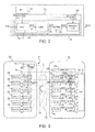
- Figures 3 and 4 diagrammatically show two possible different photonic-assisted architectures of the receiving section 4 of a radar system 1, wherein the active electronically-scanned antenna 2 comprises a plurality of antenna subarrays 29 connected to the digital signal processor 9 by means of a photonic-assisted analog-to-digital converter 8 which comprises the mode-locked laser device 11 generating the optical clock signal SS and a plurality of photonic-assisted analog-to-digital conversion stages 21, each of which connects a relative antenna subarray 29 to the digital signal processor 9, and is adapted to receive a pulsed optical carrier obtained on the basis of the optical clock signal obtained on the basis of the optical clock signal SS generated by the single mode-locked laser device 11.
- a photonic-assisted analog-to-digital converter 8 which comprises the mode-locked laser device 11 generating the optical clock signal SS and a plurality of photonic-assisted analog-to-digital conversion stages 21, each of which connects a relative antenna subarray 29 to the digital signal processor 9, and is
- the architecture of the receiving section 4 shown in figure 3 finds advantageous, but not exclusive application in so-called “multirole” radar systems 1, i.e. systems equipped with a multichannel active electronically-scanned receiving antenna 2, and known as “M-AESA radars” (Multirole Active Electronically Scanned Array - M-AESA).
- M-AESA radars Multirole Active Electronically Scanned Array - M-AESA
- the antenna 2 comprises a revolving antenna portion indicated by reference numeral 30, in which the antenna subarrays are housed 29; and a fixed antenna portion, indicated by reference numeral 31, which accommodates the digital signal processor 9, and may be arranged under the revolving portion 30 so as to form the support base of the revolving antenna itself or, alternatively, may be arranged in a remote portion with respect to the revolving antenna 30 portion itself.
- the receiving section 4 of the multichannel active electronically-scanned antenna 2 shown in figure 3 has an architecture in which the photonic-assisted analog-to-digital conversion stages 21 associated to the antenna subarrays 29 each have the respective electro-optical modulating unit 14 housed in the revolving antenna portion 30, while the remaining components, i.e. the electro-optical detection unit 16 and the electronic analog-to-digital converter 13 are arranged in the fixed antenna portion 31.
- the architecture of the receiving section 4 of the active electronically-scanned antenna multi-receiver includes that the mode-locked laser device 11 is housed in the revolving antenna portion 30, while the electro-optical detection unit 23 generating the electric clock signals CK3 to be supplied to the electronic analog-to-digital converters 13 is housed in the fixed antenna portion 31.
- the architecture of the receiving section 4 of the active electronically-scanned multi-receiver antenna 2 further includes that the sampled optical signal SO1 generated by each electro-optical modulating unit 14 and the optical clock signal SS generated by the mode-locked laser device 11 are communicated to the electro-optical detection unit 16 and to the electro-optical detection unit 23, respectively, by means of the optical means 15 arranged in the revolving joint 32 coupled to the revolving antenna portion 30 and/or to the fixed antenna portion 31.
- the electric sampling signals SEC are advantageously processed by the digital signal processor 9 which is arranged in a remote position with respect to the position of the revolving antenna portion 30, while the flow of light pulses which form the sampled optical signal SO1 and cross the optical means 15 in the revolving joint 32 may be obtained by means of modulating techniques of the Wavelength Domain Multiplexing type.
- the architecture of the receiving section 4 shown in figure 4 finds advantageous, but not exclusive application in M-AESA radar systems 1 provided with a fixed type active electronically-scanned multi-receiver antenna 2, thus provided with a fixed antenna portion 31.
- the architecture shown in figure 4 differs from the architecture shown in figure 3 because the fixed antenna portion 31 houses: the antenna subarrays 29, the mode-locked laser device 11 and the photonic-assisted analog-to-digital conversion 21 associated to the antenna subarrays 29.
- Figure 5 diagrammatically illustrates a different architecture of the receiving section 4 of a radar system 1, in which the multi-receiver active electronically-scanned antenna comprises an analog RF beamformer device 33 operating in the RF signal domain, which receives as input the electric analog signals SE2 associated to the RF signals SF2 received from the antenna subarrays 29, and is configured to combine the electric analog signals SE2 themselves (in known manner and therefore not described in detail) to output three electric analog signals ⁇ , ⁇ az and ⁇ el, which are indicative of the angular form (Gaussian form etc.), the swinging angle or azimuth and the elevation angle of the antenna beam, respectively.
- the multi-receiver active electronically-scanned antenna comprises an analog RF beamformer device 33 operating in the RF signal domain, which receives as input the electric analog signals SE2 associated to the RF signals SF2 received from the antenna subarrays 29, and is configured to combine the electric analog signals SE2 themselves (in known manner and therefore not described in detail) to output three electric analog signals ⁇ ,
- the architecture shown in figure 5 further includes a photonic-assisted analog-to-digital converter 8 provided with three photonic-assisted analog-to-digital conversion stages 21, which receive in input the optical clock signal SS generated by the mode-locked laser device 11, and the three analog signals ⁇ , ⁇ az, and ⁇ el, and output the electric signals ⁇ , ⁇ az, ⁇ el in the digital format to be fed to the digital signal processor 9 which processes them to determine the required radar information.
- a photonic-assisted analog-to-digital converter 8 provided with three photonic-assisted analog-to-digital conversion stages 21, which receive in input the optical clock signal SS generated by the mode-locked laser device 11, and the three analog signals ⁇ , ⁇ az, and ⁇ el, and output the electric signals ⁇ , ⁇ az, ⁇ el in the digital format to be fed to the digital signal processor 9 which processes them to determine the required radar information.
- the architecture shown in figure 5 finds advantageous, but not exclusive application in the M-AESA radar systems 1 provided with a revolving antenna portion 30, a fixed antenna portion 31 and a revolving joint 32.
- the revolving antenna portion 30 houses the antenna subarrays 29 and the analog RF beamformer device 33, while the fixed antenna portion 31 houses the mode-locked laser device 11, the three photonic-assisted analog-to-digital conversion stages 21, the electro-optical detection unit 23 configured to provide the electric clock signals CK3 to each electric analog-to-digital converter 13 on the basis of the optical clock signal SS produced by the mode-locked laser device 11; and the digital signal processor 9.
- the beam signals ⁇ , ⁇ az, and ⁇ el generated by the analog RF beamformer device 33 are supplied to the photonic-assisted analog-to-digital converter 8 by means of the electric means (not shown) arranged in the revolving joint 32.
- the architecture of the receiving section 4 shown in figure 6 finds advantageous, but not exclusive application in M-AESA radar systems 1 provided only with a fixed antenna portion 31.
- the architecture shown in figure 6 differs from the architecture shown in figure 5 because, on one hand, it does not include the use of a revolving joint and, on the other hand, the fixed antenna portion 31 also houses the electro-optical detection unit 22, the mode-locked laser device 11 and the three photonic-assisted analog-to-digital conversion 8, in addition to the antenna subarrays 29 and the analog RH beamformer device 33.
- Figure 7 diagrammatically shows a different architecture of the receiving section 4 of a radar system 1, advantageously, but not exclusively applicable in instantaneously broad band radar applications, such as, for example, electronic war applications, or M-AESA antenna systems.
- the photonic-assisted analog-to-digital conversion stage 21 comprises an interleaving switch detect unit 40, which is configured so as to: receive in input the sampled optical signal SO1 generated by the electro-optical modulation unit 14 on the basis of a sampling frequency associated to the optical clock signal SS; and implements a parallelization of the sampled optical signal SO1 so as to obtain/output a plurality of electric analog sampling signals SEC having frequencies lower than the optical sampling frequency.
- the interleaving switch detect unit 40 supplies the analog electric sampling signals SEC to a plurality of electronic analog-to-digital converters 13, which convert them into electric digital signals SED.
- Such electronic converters ADC may have an operating band which is the tenth of that of the sampling contained in SO1.
- the electronic analog-to-digital converters 13 operate on the basis of electric clock signals CK3 obtained by means of an electro-optical detection unit 23, which may be configured, in turn, so as to manage the sequence of high speed optical pulses of the optical clock signal SS generated by the mode-locked laser device 11 by means of modulating techniques of the WDM (Wavelength Division Multiplexing) type or of the TDM (Time Division Multiplexing) type.
- WDM Widelength Division Multiplexing
- TDM Time Division Multiplexing
- Figure 8 shows a possible application of the architecture shown in figure 7 in a radar system 1 provided with an active electronically-scanned multi-receiver antenna 2 comprising a plurality of antenna subarrays 29.
- the antenna subarrays 29 are connected to the digital signal processor 9 by means of a plurality of photonic-assisted analog-to-digital conversion stages 21, each of which is provided with an interleaving switch detect unit 40.
- the receiving section 4 of the radar system 1 shown in figure 8 by virtue of the configuration described above allows to advantageously reduce the sampling speed of the electronic analog-to-digital sampling converter 13 and thus obtain a better dynamic, i.e. a better actual effective number of bits ENOB at the output of the electronic analog-to-digital converters 13 themselves.
- the radar system described above is extremely advantageous because, in addition to carrying out the complete digitalization of the RF radar signal in a broad band, allows to use the optical clock signal generated by the MLL present in the photonic-assisted analog-to-digital converter to obtain the electric clock signals present in the radar system itself.
- the use of the optical clock signal further determines a drastic reduction of the electromagnetic interference with respect to the known radar systems.
Landscapes
- Engineering & Computer Science (AREA)
- Radar, Positioning & Navigation (AREA)
- Remote Sensing (AREA)
- Computer Networks & Wireless Communication (AREA)
- Physics & Mathematics (AREA)
- General Physics & Mathematics (AREA)
- Theoretical Computer Science (AREA)
- Radar Systems Or Details Thereof (AREA)
- Optical Radar Systems And Details Thereof (AREA)
Abstract
Description
- The present invention relates to a photonic-assisted digital radar system, and in particular to a multirole, multifunctional radar equipped with an active electronically-scanned antenna (AESA), to which the following description will refer without losing in generality.
- As is known, for example, from
US 5, 117, 239 , radar systems comprise an antenna configured to receive and transmit RF (radiofrequency) signals; a transmitting section connected to the antenna and configured to generate and transmit RF signals by means of the antenna; and a receiving section connected to the antenna and configured to receive and process RF signals received from the antenna, shift them to base band or to an intermediate frequency, and convert them into corresponding digital signals, which are then appropriately processed. - In particular, the transmitting section comprises a waveform generator (WG), configured to generate a modulating signal constituted by a pulsed waveform; and a modulator, configured to modulate a carrier with the modulating signal and supply the RF signal thus generated to the antenna for transmission.
- The receiving section comprises instead an analog-to-digital converter (ADC) configured to receive the RF signals received by the antenna or the corresponding base band or intermediate frequency signals and convert them into digital signals; and a digital signal processor (DSP) configured to receive and process the digital signals supplied by the analog-to-digital converter and appropriately process them.
- The analog-to-digital conversion of the RF signals received by the antenna includes a sampling thereof by means of a sampling signal supplied by an appropriate electronic clock device. Currently, the maximum sampling frequency which can be reached is in the order of a few GHz mainly due to the electromagnetic interferences to which the analog-to-digital converters are prone during the operation thereof and to the performance limitations of the electronic devices used, and therefore this type of analog-to-digital conversion architecture is in fact not usable in all those applications in which sampling in the order of several tens of GHz is needed.
- For this purpose, the use of electronic analog devices instead of digital devices in the receiving section has been suggested. However, such a solution is not practical because the non-linear behavior and the high phase noise introduced by the electronic analog devices cause a limitation of the performance of the radar systems both in terms of signal reception and in terms of coherent data processing.
- The present invention originates from the idea of using known photonic-assisted analog-to-digital converters in radar systems, wherein an electric analog signal to be converted into digital is first converted into a corresponding optical signal, then optically sampled, and then reconverted into a corresponding electric digital signal.
- In this type of analog-to-digital converters, the electronic analog signal modulates a pulsed optical carrier constituted by light pulses of duration in the order of picoseconds (10-12s) this being an operation which corresponds to an optical sampling of the electric analog signal, and the optical signal thus generated is then converted into an electric digital signal by means of appropriate electro-optical converter devices, typically photodiodes.
- An example of a photonic-assisted analog-to-digital converter is described in
US 6.771.201 . - The Applicant has thus conducted an in-depth study aimed at identifying an architecture of the reception and transmission sections which, by exploiting the features of the photonic-assisted analog-to-digital converters allows to improve the performance of the radar systems as a whole.
- According to the present invention, a photonic-assisted digital radar system is provided, as claimed in the appended claims.
- In broad outline, in the photonic-assisted digital radar system according to the present invention an optical clock signal generated by a single mode-locked laser device (MLL device) in the photonic-assisted analog-to-digital converter is used for both carrying out the photonic-assisted analog-to-digital conversion as described above and for advantageously timing a plurality of electronic devices present in the photonic-assisted digital radar system.
-
-
Figure 1 diagrammatically shows a photonic-assisted digital radar system, made according to the dictates of the present invention; -
Figure 2 diagrammatically shows a photonic-assisted analog-to-digital converter used in the photonic-assisted digital radar system shown inFigure 1 ; -
Figure 3 diagrammatically shows a first architecture of the photonic-assisted digital radar system made according to the dictates of the present invention; -
Figure 4 diagrammatically shows a second architecture of the photonic-assisted digital radar system made according to the dictates of the present invention; -
Figure 5 diagrammatically shows a third architecture of the photonic-assisted digital radar system made according to the dictates of the present invention; -
Figure 6 diagrammatically shows a fourth architecture of the photonic-assisted digital radar system made according to the dictates of the present invention; -
Figure 7 diagrammatically shows a fifth architecture of the photonic-assisted digital radar system made according to the dictates of the present invention; while -
Figure 8 diagrammatically shows a sixth architecture of the photonic-assisted digital radar system made according to the dictates of the present invention. - The present invention will now be described in detail with reference to the accompanying figures in order to allow a person skilled in the art to make it and use it. Various changes to the described embodiments will be immediately apparent to a person skilled in the art, and the described generic principles may be applied to other embodiments and applications without therefore departing from the scope of protection of the present invention, as defined in the appended claims. Thus, the present invention must not be considered limited to the described and illustrated embodiments but instead confers the broadest scope of protection, in accordance with the principles and features described and claimed herein.
- With reference to
Figure 1 ,reference numeral 1 indicates as a whole a photonic-assisted digital radar system essentially comprising: anantenna 2; a transmittingsection 3 connected to theantenna 2 and configured to generate and transmit RF signals SF1 by means of theantenna 2 itself; and areceiving section 4 connected to theantenna 2 and configured to receive and process the RF signals SF2. - The
antenna 2 is of the active electronically-scanned type, also known as "phased-array" antenna, comprising a plurality of antenna subarrays configured to generate an antenna beam which scans the space to allow to carry out multiple radar functions, such as for example airspace surveillance, and/or target tracking functions and/or missile guiding functions and/or electronic war (EW) functions. - In particular, the phased-array antenna may comprise a fixed antenna, or a revolving antenna, which is coupled to a frame or supporting base (not shown) by means of electro-mechanical revolving members, e.g. a revolving joint (of the known type and not shown), structured to revolve the antenna with respect to the support base about a predetermined revolution axis (not shown), preferably a vertical axis.
- According to a preferred embodiment shown in
figure 1 , the transmittingsection 3 comprises awaveform generator 5 configured to generate a pulsed waveform constituted by a modulating electric signal SWG comprising a sequence of electric transmission radar pulses; and amixer 6, which is configured to receive in input an electric transmission carrier STALO and the modulating signal SWG so as to generate the RF signal SF1 to be transmitted by means of theantenna 2. - In particular, the
waveform generator 5 is configured so as to receive as input an electrical clock signal CK1 and time the generation of the electric transmission pulses which compose the electric modulating signal SWG on the basis of the received electric clock signal CK1. - The
mixer 6 is connected to the output of a filter 7, e.g. a band-pass filter, which is, in turn, configured so as to receive an electrical clock signal CK2 as input, and appropriately filters the electronic clock signal CK2 itself so as to supply the transmission carrier STALO to themodulator 6. - With reference to the embodiment shown in
figure 1 , thereceiving section 4 comprises a photonic-assisted analog-to-digital converter 8, which receives an electric analog signal SE2, echo of the RF signal SF2, from theantenna 2 by means of a pass-band pre-selectortype filter 10, carries out an optical sampling of the electric analog signal SE2 so as to obtain a sampled optical signal SO1, and converts the sampled optical signal SO1 into a corresponding electric digital signal. - In other words, the photonic-assisted analog-to-
digital converter 8 is configured to modulate by means of the electric analog signal SE2 a pulsed optical carrier constituted by light pulses in the order of picoseconds (10-12 s) to obtain an optical sampling of the analog signal SE2 itself, operating in a high frequency electric analog signal domain SE2, i.e. comprised in a first band of frequencies, indicated hereinafter as "broad band" associated to the overall operative band of theradar system 1, and corresponding to a frequency interval comprised between approximately 0 and 20-40 GHz, preferably 0-35 GHz; - converting the sampled optical signal SO1, obtained from the sampling, into an electric analog sampled signal SEC;
- digitalizing the electric analog sampled signal SEC so as to obtain an electric digital signal SED, operating both in the domain of the optical signals SO1, and in the domain of the electric analog sampled signals SEC, at an intermediate frequency comprised in a second frequency band, indicated hereinafter as "instantaneous band", associated to the operative band actually available in reception.
- In the description above it is worth noting that if the analog signal in the operating band SE2 is a fractional narrow band, the extensions of the instantaneous band may even be lower than the operating band for some functions.
- In such a case, the photonic-assisted analog-to-
digital converter 8 downsamples the analog signal SE2 thus obtaining the intermediate bands sampled optical signal SO1. Implicitly, the photonic-assisted analog-to-digital converter 8 carries out a down-conversion in the "instantaneous band" of the electric analog sampled signal SEC. - The receiving
section 4 is further provided with a processing unit comprising, for example, adigital signal processor 9, which is configured to receive and appropriately process the electric digital signal SED. - In the preferred embodiment shown in
figures 1 and2 , the photonic-assisted analog-to-digital converter 8 comprises a mode-lockedlaser device 11, which is configured to generate the optical clock signal SS comprising a sequence of light pulses, each having a duration in the order of picoseconds (10-12 s); and a photonic-assisted analog-to-digital conversion stage 21, which comprises, in turn, an electro-optical sampler-converter 12, which receives the electric analog signal SE2 and the optical clock signal SS as input and outputs an electric analog sampled signal SEC; and an electronic analog-to-digital converter 13, which receives the electric analog sampled signal SEC as input, and is configured so as to convert the electric analog sampled signal SEC into the electric digital signal SED. - In particular, the electro-optical sampler-
converter 12 is configured to modulate a pulsed optical carrier corresponding to the optical clock signal SS on the basis of the electric analog signal SE2 so as to generate the sampled optical signal SO1 comprising the optical samples associated to the electric analog signal SE2, and converts the sampled optical signal SO1 itself into the electric analog sampled signal SEC comprising the electric samples associated to the optical samples. - According to the preferred embodiment shown in
figure 2 , the electro-optical sampler-converter device 12 is provided with an electro-optical modulatingunit 14, preferably comprising a Mach-Zender modulator, which has an optical input connected to the output of the mode-lockedlaser device 11 by means ofoptical means 15 for receiving the optical clock signal SS; an electric signal connected to thefilter 10 to receive the electric analog signal SE2; and an output generating the sampled optical signal SO1. - In particular, the electro-optical modulating
unit 14 is configured to modulate the pulsed optical carrier on the basis of the electric analog signal SE2 so as to generate the sampled optical signal SO1. - In the description above it is worth noting that the pulsed optical carrier SS used by the electro-optical modulating
unit 14 may have a frequency lower than the radar signal frequency SF2, if it is fractional narrow band, and thus the radar signal SF2 may be subjected to downsampling. This is possible, by maintaining a high dynamic of the electric analog sampled signal SEC, by virtue of the high time stability of the pulsed optical carrier SS (jitter rms <10^-14 sec). - The electro-optical sampler-
converter device 12 is further provided with an electro-optical detection unit 16, which is optically coupled to the electro-optical modulatingunit 14, by means ofoptical means 15, for receiving in the latter the sampled optical signal SO1, and unlike the converter described inUS6771201 , is configured to convert the sampled optical signal SO1 into the electric analog sampled signal SEC operating withelectronic converters ADC 13 available at instantaneous band frequencies. - According to the preferred embodiment shown in
figure 2 , the electro-optical detection unit 16 may be provided with at least one electro-optical converter comprising a photodiode (not shown), which is controlled by electronic control means (not shown) to time the conversion of the sampled optical signal SO1 into the electric analog sampled signal SEC. - The photonic-assisted analog-to-
digital converter 8 further comprises afilter 20, e.g. a Nyquist anti-aliasing low-pass filter, which receives as input the electric sampling signal SEC and filters the latter in the instantaneous band so as to input it to the electronic analog-to-digital converter 13. - According to the preferred embodiment shown in
figures 1 and2 , the optical clock signal SS generated by the mode-lockedlaser device 11, in addition to being conveniently used by theradar system 1 as pulsed optical carrier for obtaining the sampled optical signal SO1 by modulating, is advantageously used to obtain the electric clock signals CK1, CK3, CK4 used by thewaveform generator 5, by the electronic analog-to-digital converter 13 and by the signaldigital processor 9, respectively. - For this purpose, the
radar system 1 comprises a series of electro-optical detection units laser device 11 by means ofoptical means 15 for generating the optical clock signal SS, and output the respective electric clock signals CK1, CK3 and CK4, to be supplied to thewaveform generator 5, to the electronic analog-to-digital converter 13, and to thedigital signal processor 9, respectively. - In other words, the
waveform generator 5, the electronic analog-to-digital converter 13, and thedigital signal processor 9 operate, i.e. are timed, independently from each other, on the basis of corresponding electric clock signals CK1, CK3 and CK4 respectively, each of which is obtained from the optical clock signal SS, preferably, but not necessarily by means of an appropriate frequency adaptation/reduction. - In the case in point, the electro-optical detection unit 22 is connected to the mode-locked
laser device 11 by means of afrequency splitter device 22a (splitting 1:N), which is configured to receive as input the optical clock signal SS so as to output it at a reduced frequency, thus suited for generating the electric clock signal CK1 to be supplied to thewaveform generator 5. - According to the preferred embodiment shown in
figure 1 , the optical clock signal SS generated by the mode-lockedlaser device 11, in addition to being used by theradar system 1 as pulsed optical carrier of the optical signal SO1 and clock reference for generating electric clock signals CK1, CK3 and CK4, is conveniently used for generating the electric clock signal CK2 used to generate the electric transmission carrier STALO to supply to themodulator 6. - For this purpose, the
radar system 1 comprises a further electro-optical detection unit 25, which has an input optically connected to the output of the mode-lockedlaser device 11, by means ofoptical means 15 to receive the optical clock signal SS, and outputs the electric carrier STALO which it supplies to themodulator 6, by means of the filter 7. - In the description above it is worth noting that the architecture of the electro-
optical detection units optical detection unit 16, i.e. may be provided with an electro-optical converter comprising a photodiode configured to convert (in known manner and thus not described in detail) the light pulses into electric pulses having an appropriate reduced frequency according to the timing of the electronic device to which they are supplied, while theoptical means 15 may be made by means of wave guides comprising optical filters for transmitting the optical clock signal SS. - In the description above, it is further worth noting that the frequency of the electric clock signal CK2 used for generating the electric carrier STALO to be inputted to the
mixer 6 is different from the frequency of the optical clock signal SS (the two signals cannot be multiples) so as to ensure a correct execution of the optical sampling by means of an electro-optical modulatingunit 14 and the electro-optical detection unit 16. - The
receiving section 4 of theradar system 1 described above may be advantageously made according to different architectures, in each of which an optical clock signal SS generated by the single mode-lockedlaser device 11 present in the photonic-assisted analog-to-digital converter 8 is used for both carrying out the photonic-assisted analog-to-digital conversion of the electric sampling signal SE2 analog into the digital signal SED and for generating the electric clock signals CK1, CK2, CK3 and CK4. -
Figures 3 and4 diagrammatically show two possible different photonic-assisted architectures of the receivingsection 4 of aradar system 1, wherein the active electronically-scannedantenna 2 comprises a plurality ofantenna subarrays 29 connected to thedigital signal processor 9 by means of a photonic-assisted analog-to-digital converter 8 which comprises the mode-lockedlaser device 11 generating the optical clock signal SS and a plurality of photonic-assisted analog-to-digital conversion stages 21, each of which connects arelative antenna subarray 29 to thedigital signal processor 9, and is adapted to receive a pulsed optical carrier obtained on the basis of the optical clock signal obtained on the basis of the optical clock signal SS generated by the single mode-lockedlaser device 11. - In particular, the architecture of the receiving
section 4 shown infigure 3 finds advantageous, but not exclusive application in so-called "multirole"radar systems 1, i.e. systems equipped with a multichannel active electronically-scanned receivingantenna 2, and known as "M-AESA radars" (Multirole Active Electronically Scanned Array - M-AESA). - In the preferred embodiment shown in
figure 3 , theantenna 2 comprises a revolving antenna portion indicated byreference numeral 30, in which the antenna subarrays are housed 29; and a fixed antenna portion, indicated byreference numeral 31, which accommodates thedigital signal processor 9, and may be arranged under the revolvingportion 30 so as to form the support base of the revolving antenna itself or, alternatively, may be arranged in a remote portion with respect to the revolvingantenna 30 portion itself. - The receiving
section 4 of the multichannel active electronically-scannedantenna 2 shown infigure 3 has an architecture in which the photonic-assisted analog-to-digital conversion stages 21 associated to theantenna subarrays 29 each have the respective electro-optical modulating unit 14 housed in the revolvingantenna portion 30, while the remaining components, i.e. the electro-optical detection unit 16 and the electronic analog-to-digital converter 13 are arranged in the fixedantenna portion 31. - In particular, the architecture of the receiving
section 4 of the active electronically-scanned antenna multi-receiver includes that the mode-lockedlaser device 11 is housed in the revolvingantenna portion 30, while the electro-optical detection unit 23 generating the electric clock signals CK3 to be supplied to the electronic analog-to-digital converters 13 is housed in the fixedantenna portion 31. - The architecture of the receiving
section 4 of the active electronically-scannedmulti-receiver antenna 2 further includes that the sampled optical signal SO1 generated by each electro-optical modulating unit 14 and the optical clock signal SS generated by the mode-lockedlaser device 11 are communicated to the electro-optical detection unit 16 and to the electro-optical detection unit 23, respectively, by means of the optical means 15 arranged in the revolving joint 32 coupled to the revolvingantenna portion 30 and/or to the fixedantenna portion 31. - Furthermore, it is worth noting that the electric sampling signals SEC are advantageously processed by the
digital signal processor 9 which is arranged in a remote position with respect to the position of the revolvingantenna portion 30, while the flow of light pulses which form the sampled optical signal SO1 and cross the optical means 15 in the revolving joint 32 may be obtained by means of modulating techniques of the Wavelength Domain Multiplexing type. - Instead, the architecture of the receiving
section 4 shown infigure 4 finds advantageous, but not exclusive application in M-AESA radar systems 1 provided with a fixed type active electronically-scannedmulti-receiver antenna 2, thus provided with a fixedantenna portion 31. - In particular, the architecture shown in
figure 4 differs from the architecture shown infigure 3 because the fixedantenna portion 31 houses: theantenna subarrays 29, the mode-lockedlaser device 11 and the photonic-assisted analog-to-digital conversion 21 associated to theantenna subarrays 29. - In the description above it is worth emphasizing that the architectures shown in
figures 3 and4 are both conveniently adapted to be used in M-AESA radar systems because they allow to obtain the antenna beam associated to theantenna subarrays 29 directly in the electric digital domain, conveniently by using a single optical clock signal in the antenna "front-end", available by virtue of the presence of the mode-lockedlaser device 11 contained in the photonic-assisted analog-to-digital converter 8. -
Figure 5 diagrammatically illustrates a different architecture of the receivingsection 4 of aradar system 1, in which the multi-receiver active electronically-scanned antenna comprises an analogRF beamformer device 33 operating in the RF signal domain, which receives as input the electric analog signals SE2 associated to the RF signals SF2 received from theantenna subarrays 29, and is configured to combine the electric analog signals SE2 themselves (in known manner and therefore not described in detail) to output three electric analog signals Σ, Δaz and Δel, which are indicative of the angular form (Gaussian form etc.), the swinging angle or azimuth and the elevation angle of the antenna beam, respectively. - The architecture shown in
figure 5 further includes a photonic-assisted analog-to-digital converter 8 provided with three photonic-assisted analog-to-digital conversion stages 21, which receive in input the optical clock signal SS generated by the mode-lockedlaser device 11, and the three analog signals Σ, Δaz, and Δel, and output the electric signals Σ, Δaz, Δel in the digital format to be fed to thedigital signal processor 9 which processes them to determine the required radar information. - Similarly to the architecture shown in
figure 3 , the architecture shown infigure 5 finds advantageous, but not exclusive application in the M-AESA radar systems 1 provided with a revolvingantenna portion 30, a fixedantenna portion 31 and a revolvingjoint 32. - In particular, the revolving
antenna portion 30 houses the antenna subarrays 29 and the analogRF beamformer device 33, while the fixedantenna portion 31 houses the mode-lockedlaser device 11, the three photonic-assisted analog-to-digital conversion stages 21, the electro-optical detection unit 23 configured to provide the electric clock signals CK3 to each electric analog-to-digital converter 13 on the basis of the optical clock signal SS produced by the mode-lockedlaser device 11; and thedigital signal processor 9. - The beam signals Σ, Δaz, and Δel generated by the analog
RF beamformer device 33 are supplied to the photonic-assisted analog-to-digital converter 8 by means of the electric means (not shown) arranged in the revolvingjoint 32. - Similarly to the architectures shown in
figure 4 , the architecture of the receivingsection 4 shown infigure 6 finds advantageous, but not exclusive application in M-AESA radar systems 1 provided only with a fixedantenna portion 31. - In particular, the architecture shown in
figure 6 differs from the architecture shown infigure 5 because, on one hand, it does not include the use of a revolving joint and, on the other hand, the fixedantenna portion 31 also houses the electro-optical detection unit 22, the mode-lockedlaser device 11 and the three photonic-assisted analog-to-digital conversion 8, in addition to the antenna subarrays 29 and the analogRH beamformer device 33. -
Figure 7 diagrammatically shows a different architecture of the receivingsection 4 of aradar system 1, advantageously, but not exclusively applicable in instantaneously broad band radar applications, such as, for example, electronic war applications, or M-AESA antenna systems. - In particular, in the architecture shown in
figure 7 , the photonic-assisted analog-to-digital conversion stage 21 comprises an interleaving switch detectunit 40, which is configured so as to: receive in input the sampled optical signal SO1 generated by the electro-optical modulation unit 14 on the basis of a sampling frequency associated to the optical clock signal SS; and implements a parallelization of the sampled optical signal SO1 so as to obtain/output a plurality of electric analog sampling signals SEC having frequencies lower than the optical sampling frequency. - The interleaving switch detect
unit 40 supplies the analog electric sampling signals SEC to a plurality of electronic analog-to-digital converters 13, which convert them into electric digital signals SED. Such electronic converters ADC may have an operating band which is the tenth of that of the sampling contained in SO1. - The electronic analog-to-
digital converters 13 operate on the basis of electric clock signals CK3 obtained by means of an electro-optical detection unit 23, which may be configured, in turn, so as to manage the sequence of high speed optical pulses of the optical clock signal SS generated by the mode-lockedlaser device 11 by means of modulating techniques of the WDM (Wavelength Division Multiplexing) type or of the TDM (Time Division Multiplexing) type. -
Figure 8 shows a possible application of the architecture shown infigure 7 in aradar system 1 provided with an active electronically-scannedmulti-receiver antenna 2 comprising a plurality ofantenna subarrays 29. - The antenna subarrays 29 are connected to the
digital signal processor 9 by means of a plurality of photonic-assisted analog-to-digital conversion stages 21, each of which is provided with an interleaving switch detectunit 40. - In the description above it is worth specifying that the receiving
section 4 of theradar system 1 shown infigure 8 , by virtue of the configuration described above allows to advantageously reduce the sampling speed of the electronic analog-to-digital sampling converter 13 and thus obtain a better dynamic, i.e. a better actual effective number of bits ENOB at the output of the electronic analog-to-digital converters 13 themselves. - The radar system described above is extremely advantageous because, in addition to carrying out the complete digitalization of the RF radar signal in a broad band, allows to use the optical clock signal generated by the MLL present in the photonic-assisted analog-to-digital converter to obtain the electric clock signals present in the radar system itself. The use of the optical clock signal further determines a drastic reduction of the electromagnetic interference with respect to the known radar systems.
- It is finally apparent that changes and variations can be made to that described and illustrated above without departing from the scope of protection of the present invention, as defined in the appended claims.
Claims (7)
- A photonic-assisted digital radar system (1) comprising:- an active electronically-scanned antenna (2);- a transmitting section (3) connected to the antenna (2) and configured to generate and transmit RF signals (SF1) via the antenna (2); and- a receiving section (4) connected to the antenna (2) and configured to receive and process electric analog signals (SE2) associated to received RF signals (SF2);the transmitting section (3) comprising:- a waveform generator (5) configured to generate an electric modulating signal in the form of a pulsed waveform (SWG); and- a modulator (6) configured to receive an electric transmission carrier (STALO) and the electric modulating signal (SWG) and to modulate the transmission carrier (STALO) by means of the modulating signal (SWG), thereby generating a radiofrequency signal (SF1) to be transmitted via the antenna (2);characterized in that the receiving section (4) comprises:- photonic-assisted analog-to-digital converting means (8) configured to convert electric analog signals (SE2) into corresponding electric digital signals (SED); and- digital signal processing means (9) configured to receive and process the electric digital signals (SED);wherein the photonic-assisted analog-to-digital converting means (8) comprises:- a mode-locked laser device (11) configured to generate an optical clock signal (SS); and- electronic analog-to-digital converting means (13); the electronic analog-to-digital converter means (13), the waveform generator (5), the modulator (6) and the digital signal processing means (9) being configured to operate based on respective electric clock signals (CK3),(CK1),(CK2),(CK4) generated based on the optical clock signal (SS).
- A system according to claim 1, wherein the photonic-assisted analog-to-digital converting means (8) comprises at least one photonic-assisted analog-to-digital converting stage (21) comprising:- at least one modulating unit (14) configured to modulate an optical pulsed carrier obtained based on the optical clock signal (SS) by means of an electric analog signal (SE2) associated to an RF signal (SF2) received by the antenna (2), thereby generating an optical sampled signal (SO1) containing samples of the electric analog signal (SE2) received by the antenna (2);- at least one electro-optical detection unit (16) configured to convert an optical sampled signal (SO1) into a corresponding electric analog sampled signal (SEC);- at least one electronic analog-to-digital converter (13) configured to convert the electric analog sampled signal (SEC) into a corresponding electric digital signal (SED) for the digital signal processing means (9).
- A system according to claim 1, wherein a frequency of the optical clock signal (SS) is lower than, and not a submultiple of, a frequency of a received RF signal (SF2); the photonic-assisted analog-to-digital converting means (8) being configured to sub-sample the corresponding electric analog signal (SE2), so as to carry out a down-conversion of the instantaneous frequency band of the electric analog sampled signal (SEC) and obtain the optical sampled signal (SO1) with an intermediate frequency band.
- A system according to claims 2 or 3, wherein the antenna (2) is designed to house at least one electro-optical modulating unit (14) operable to generate the optical sampled signal (SO1), and at least one interleaving device (40) configured to receive the optical sampled signal (SO1) from the electro-optical modulating unit (14); parallelize the optical sampled signal (SO1) to output a plurality of electric analog sampled signals (SEC) with frequencies lower than a frequency of the optical clock signal (SS); and supply the electric analog sampled signals (SEC) to corresponding electronic analog-to-digital converters (13) operable to convert the electric analog sampled signals (SEC) into corresponding electric digital radar signals (SED).
- A system according to claims 2 or 3, wherein the antenna (2) is a phased array antenna comprising a fixed antenna base (31) and an antenna portion (30) rotatably mounted on the antenna base (31) and comprising a plurality of antenna subarrays (29), each of which is configured to output an electric analog signal (SE2) associated to a corresponding RF signal (SF2) received by the antenna subarray (29);
the antenna portion (30) being designed to house the mode-locked laser device operable to generate the optical clock signal (SS);
the antenna base (31) being designed to house:- a plurality of electro-optical detecting units (16) configured to receive sampled optical signals (SO1) from the corresponding electro-optical modulating units (14) through optical means (15) arranged in a rotary joint (32) associated to the antenna portion (30), and to convert the sampled optical signals (SO1) into corresponding electric analog sampled signals (SEC);- a plurality of electronic analog-to-digital converters (13) configured to operate based on corresponding electric clock signals (CK3) obtained based on the optical clock signal (SS) to convert the electric analog sampled signals (SEC) associated to the sampled optical signals (SO1), into respective electric digital signals (SED); e- digital signal processing means (9) configured to process the electric digital signals (SED). - A system according to claims 2 or 3, wherein the antenna (2) comprises a fixed antenna portion (31) configured to house:- the mode-locked laser device (11);- a plurality of photonic-assisted analog-to-digital converting stages (21) configured to receive the electric analog signals (SE2) associated to the RF signals (SF2) received by the antenna subarrays (29); optically sample the electric analog signals (SE2) to obtain corresponding sampled optical signals (SO1); convert the sampled optical signals (SO1) into corresponding electric analog sampled signals (SEC); and then convert the electric analog sampled signals (SEC) associated to the sampled optical signals (SO1) into corresponding electric digital signals (SED).
- A system according to claims 2 or 3, wherein the antenna (2) is a phased array antenna comprising a fixed antenna base (31) and an antenna portion (30) rotatably mounted on the antenna base (31) and comprising a plurality of antenna subarrays (29), each of which is configured to output an electric analog signal (SE2) associated to a corresponding RF signal (SF2) received by the antenna subarray (29);
the antenna portion (30) being designed to house:- the mode-locked laser device (11) operable to generate the optical clock signal (SS);- an analog RF beamformer device (33) configured to receive the electric analog signals (SE2) associated to the RF signals (SF2) which form the antenna beam and are received by the antenna subarrays (29); and to combine the electric analog signals (SE2) to output three electric analog signals (Σ), (Δaz), and (Δel), which are indicative of the angular form, of the swinging angle or azimuth, and of the elevation angle of the antenna beam, respectively; and- photonic-assisted analog-to-digital converting means (8) configured to receive the three electric analog signals (Σ), (Δaz), (Δel) via electric means housed in a rotary joint (32) associated to the antenna portion (30); optically sample the three electric analog signals (Σ), (Δaz), (Δel) to output three corresponding sampled optical signals; convert the three sampled optical signals into three corresponding electric analog signals (Σ), (Δaz), and (Δel); and convert the three electric analog signals (Σ), (Δaz), and (Δel) into three corresponding electric digital signals (SED).
Applications Claiming Priority (1)
| Application Number | Priority Date | Filing Date | Title |
|---|---|---|---|
| ITTO20110336 | 2011-04-15 |
Publications (2)
| Publication Number | Publication Date |
|---|---|
| EP2511731A1 true EP2511731A1 (en) | 2012-10-17 |
| EP2511731B1 EP2511731B1 (en) | 2016-11-30 |
Family
ID=44555146
Family Applications (1)
| Application Number | Title | Priority Date | Filing Date |
|---|---|---|---|
| EP12164336.5A Active EP2511731B1 (en) | 2011-04-15 | 2012-04-16 | Photonic-assisted digital radar system |
Country Status (5)
| Country | Link |
|---|---|
| US (1) | US8860608B2 (en) |
| EP (1) | EP2511731B1 (en) |
| CN (1) | CN102879771B (en) |
| ES (1) | ES2615497T3 (en) |
| IT (1) | ITTO20120330A1 (en) |
Cited By (1)
| Publication number | Priority date | Publication date | Assignee | Title |
|---|---|---|---|---|
| EP3418764B1 (en) * | 2017-06-23 | 2026-03-18 | Nxp B.V. | Automotive radar system and method of synchronising an automotive radar system |
Families Citing this family (10)
| Publication number | Priority date | Publication date | Assignee | Title |
|---|---|---|---|---|
| ES2615497T3 (en) * | 2011-04-15 | 2017-06-07 | Leonardo S.P.A. | Photon assisted digital radar system |
| US9197471B1 (en) * | 2011-08-05 | 2015-11-24 | Rockwell Collins, Inc. | Optically interleaved photonic analog to digital converters |
| US10069619B1 (en) | 2011-08-05 | 2018-09-04 | Rockwell Collins, Inc. | Optical sample and hold system and method |
| US9118423B1 (en) | 2013-08-09 | 2015-08-25 | Rockwell Collins.com | Optical conversion system and method with multiple amplitude processing |
| US9356704B1 (en) | 2013-08-09 | 2016-05-31 | Rockwell Collins, Inc. | Optical conversion system and method with multiple phase processing |
| US9865982B1 (en) * | 2016-03-30 | 2018-01-09 | Rockwell Collins, Inc. | Environmentally robust and compact mode-locked laser |
| US9843398B1 (en) * | 2016-05-20 | 2017-12-12 | Rockwell Collins, Inc. | Photonic direct sampling digital receiver |
| CN106371090B (en) * | 2016-08-16 | 2019-10-25 | 上海航天测控通信研究所 | Microwave and laser integration composite radar |
| CN111431531A (en) * | 2020-03-24 | 2020-07-17 | 中科启迪光电子科技(广州)有限公司 | High-speed analog-to-digital conversion system and method based on mode-locked laser |
| US12566240B2 (en) * | 2023-10-25 | 2026-03-03 | City University Of Hong Kong | Integrated lithium niobate photonic millimeter-wave radar |
Citations (5)
| Publication number | Priority date | Publication date | Assignee | Title |
|---|---|---|---|---|
| US4929956A (en) * | 1988-09-10 | 1990-05-29 | Hughes Aircraft Company | Optical beam former for high frequency antenna arrays |
| US5051754A (en) * | 1990-08-15 | 1991-09-24 | Hughes Aircraft Company | Optoelectronic wide bandwidth photonic beamsteering phased array |
| US5117239A (en) | 1991-04-24 | 1992-05-26 | General Electric Company | Reversible time delay beamforming optical architecture for phased-array antennas |
| US6771201B1 (en) | 2003-01-24 | 2004-08-03 | The United States Of America As Represented By The Secretary Of The Navy | Hybrid photonic analog to digital converter using superconducting electronics |
| US7898464B1 (en) * | 2006-04-11 | 2011-03-01 | Lockheed Martin Corporation | System and method for transmitting signals via photonic excitation of a transmitter array |
Family Cites Families (11)
| Publication number | Priority date | Publication date | Assignee | Title |
|---|---|---|---|---|
| US4097148A (en) * | 1976-11-24 | 1978-06-27 | Hughes Aircraft Company | Mode locked laser range finder |
| US5854804A (en) * | 1996-12-13 | 1998-12-29 | Intel Corporation | Method and apparatus for synchronizing a mode locked laser with a device under test |
| US6326910B1 (en) * | 2000-11-06 | 2001-12-04 | The United States Of America As Represented By The Secretary Of The Air Force | Photonic analog-to-digital conversion using light absorbers |
| US7307266B1 (en) * | 2003-11-26 | 2007-12-11 | United States Of America As Represented By The Secretary Of The Navy | Method and apparatus for an optically clocked optoelectronic track and hold device |
| US7492795B1 (en) * | 2004-01-06 | 2009-02-17 | University Of Central Florida Research Foundation, Inc. | Ultralow noise mode-locked laser and RF sinewave source |
| US7809222B2 (en) * | 2005-10-17 | 2010-10-05 | Imra America, Inc. | Laser based frequency standards and their applications |
| US8009995B2 (en) * | 2006-01-12 | 2011-08-30 | The United States Of America As Represented By The Secretary Of The Navy | Method and apparatus for photonic digital-to-analog conversion |
| EP2324390A1 (en) * | 2008-09-18 | 2011-05-25 | Selex Sistemi Integrati S.P.A. | Switchable delays optical fibre transponder with optical generation of doppler shift |
| US8432153B2 (en) * | 2008-11-21 | 2013-04-30 | The Regents Of The University Of California | Time stretch enhanced recording scope |
| US8446305B1 (en) * | 2009-09-30 | 2013-05-21 | Rockwell Collins, Inc. | Photonic analog to digital conversion |
| ES2615497T3 (en) * | 2011-04-15 | 2017-06-07 | Leonardo S.P.A. | Photon assisted digital radar system |
-
2012
- 2012-04-16 ES ES12164336.5T patent/ES2615497T3/en active Active
- 2012-04-16 US US13/447,435 patent/US8860608B2/en active Active
- 2012-04-16 EP EP12164336.5A patent/EP2511731B1/en active Active
- 2012-04-16 CN CN201210111825.1A patent/CN102879771B/en not_active Expired - Fee Related
- 2012-04-16 IT IT000330A patent/ITTO20120330A1/en unknown
Patent Citations (5)
| Publication number | Priority date | Publication date | Assignee | Title |
|---|---|---|---|---|
| US4929956A (en) * | 1988-09-10 | 1990-05-29 | Hughes Aircraft Company | Optical beam former for high frequency antenna arrays |
| US5051754A (en) * | 1990-08-15 | 1991-09-24 | Hughes Aircraft Company | Optoelectronic wide bandwidth photonic beamsteering phased array |
| US5117239A (en) | 1991-04-24 | 1992-05-26 | General Electric Company | Reversible time delay beamforming optical architecture for phased-array antennas |
| US6771201B1 (en) | 2003-01-24 | 2004-08-03 | The United States Of America As Represented By The Secretary Of The Navy | Hybrid photonic analog to digital converter using superconducting electronics |
| US7898464B1 (en) * | 2006-04-11 | 2011-03-01 | Lockheed Martin Corporation | System and method for transmitting signals via photonic excitation of a transmitter array |
Cited By (1)
| Publication number | Priority date | Publication date | Assignee | Title |
|---|---|---|---|---|
| EP3418764B1 (en) * | 2017-06-23 | 2026-03-18 | Nxp B.V. | Automotive radar system and method of synchronising an automotive radar system |
Also Published As
| Publication number | Publication date |
|---|---|
| US20130016004A1 (en) | 2013-01-17 |
| ITTO20120330A1 (en) | 2012-10-16 |
| EP2511731B1 (en) | 2016-11-30 |
| ES2615497T3 (en) | 2017-06-07 |
| CN102879771B (en) | 2016-03-09 |
| US8860608B2 (en) | 2014-10-14 |
| CN102879771A (en) | 2013-01-16 |
Similar Documents
| Publication | Publication Date | Title |
|---|---|---|
| EP2511731B1 (en) | Photonic-assisted digital radar system | |
| Ghelfi et al. | Photonics for radars operating on multiple coherent bands | |
| CN109613510B (en) | Microwave photon radar implementation method and system for small target detection or real-time tracking imaging | |
| JP5395692B2 (en) | Meteorological radar apparatus and meteorological observation method | |
| US9197471B1 (en) | Optically interleaved photonic analog to digital converters | |
| Scotti et al. | Multi-band software-defined coherent radar based on a single photonic transceiver | |
| Gao et al. | Microwave photonic MIMO radar for high-resolution imaging | |
| Scotti et al. | In-field experiments of the first photonics-based software-defined coherent radar | |
| US9843398B1 (en) | Photonic direct sampling digital receiver | |
| Yao et al. | Demonstration of ultra-high-resolution photonics-based Kaband inverse synthetic aperture radar imaging | |
| WO2007075295A3 (en) | Linear fm radar | |
| CN111830496A (en) | Microwave photonic radar imaging system and method based on multi-channel time-division de-skew reception | |
| WO2015132772A2 (en) | Photonic-assisted rf spectrum scanner for ultra-wide band receivers | |
| Xiao et al. | A microwave photonics-based inverse synthetic aperture radar system | |
| CN108919251A (en) | One kind being based on LFMCW radar detection track devices | |
| US20230236285A1 (en) | A radar system having a photonics-based signal generator | |
| EP3365993B1 (en) | Improved photonic-assisted rf spectrum scanner for ultra-wide band receivers | |
| RU2661334C1 (en) | Tranceiver module of radio-technical signals | |
| US6509729B2 (en) | Multiple simultaneous optical frequency measurement | |
| Li et al. | An ultrahigh-resolution continuous wave synthetic aperture radar with photonic-assisted signal generation and dechirp processing | |
| KR101556067B1 (en) | Apparatus and method for phase error detection in active array antenna | |
| US20060139620A1 (en) | Method and apparatus for coherently processing signals from incoherent sources including laser signals | |
| RU2692417C2 (en) | Analog-digital receiving module of active phased antenna array | |
| Scotti et al. | Tracking of a naval target with a dual-band photonic-based coherent radar system | |
| JP2017138230A (en) | Target detection device |
Legal Events
| Date | Code | Title | Description |
|---|---|---|---|
| PUAI | Public reference made under article 153(3) epc to a published international application that has entered the european phase |
Free format text: ORIGINAL CODE: 0009012 |
|
| AK | Designated contracting states |
Kind code of ref document: A1 Designated state(s): AL AT BE BG CH CY CZ DE DK EE ES FI FR GB GR HR HU IE IS IT LI LT LU LV MC MK MT NL NO PL PT RO RS SE SI SK SM TR |
|
| AX | Request for extension of the european patent |
Extension state: BA ME |
|
| 17P | Request for examination filed |
Effective date: 20130417 |
|
| REG | Reference to a national code |
Ref country code: DE Ref legal event code: R079 Ref document number: 602012025941 Country of ref document: DE Free format text: PREVIOUS MAIN CLASS: G01S0013020000 Ipc: G01S0007280000 |
|
| RIC1 | Information provided on ipc code assigned before grant |
Ipc: G01S 13/42 20060101ALI20141002BHEP Ipc: G01S 13/02 20060101ALI20141002BHEP Ipc: G01S 7/28 20060101AFI20141002BHEP Ipc: G01S 13/66 20060101ALI20141002BHEP Ipc: G01S 13/88 20060101ALI20141002BHEP |
|
| 17Q | First examination report despatched |
Effective date: 20141027 |
|
| GRAP | Despatch of communication of intention to grant a patent |
Free format text: ORIGINAL CODE: EPIDOSNIGR1 |
|
| INTG | Intention to grant announced |
Effective date: 20160617 |
|
| GRAS | Grant fee paid |
Free format text: ORIGINAL CODE: EPIDOSNIGR3 |
|
| GRAA | (expected) grant |
Free format text: ORIGINAL CODE: 0009210 |
|
| RAP1 | Party data changed (applicant data changed or rights of an application transferred) |
Owner name: LEONARDO S.P.A. |
|
| RIN1 | Information on inventor provided before grant (corrected) |
Inventor name: DISPENZA, MASSIMILIANO Inventor name: GATTA, ALESSANDRO Inventor name: FIORELLO, ANNAMARIA Inventor name: PIERNO, LUIGI Inventor name: RICCI, MASSIMO Inventor name: SECCHI, ALBERTO |
|
| AK | Designated contracting states |
Kind code of ref document: B1 Designated state(s): AL AT BE BG CH CY CZ DE DK EE ES FI FR GB GR HR HU IE IS IT LI LT LU LV MC MK MT NL NO PL PT RO RS SE SI SK SM TR |
|
| REG | Reference to a national code |
Ref country code: CH Ref legal event code: EP Ref country code: GB Ref legal event code: FG4D |
|
| REG | Reference to a national code |
Ref country code: AT Ref legal event code: REF Ref document number: 850314 Country of ref document: AT Kind code of ref document: T Effective date: 20161215 |
|
| REG | Reference to a national code |
Ref country code: IE Ref legal event code: FG4D |
|
| REG | Reference to a national code |
Ref country code: DE Ref legal event code: R096 Ref document number: 602012025941 Country of ref document: DE |
|
| PG25 | Lapsed in a contracting state [announced via postgrant information from national office to epo] |
Ref country code: LV Free format text: LAPSE BECAUSE OF FAILURE TO SUBMIT A TRANSLATION OF THE DESCRIPTION OR TO PAY THE FEE WITHIN THE PRESCRIBED TIME-LIMIT Effective date: 20161130 |
|
| REG | Reference to a national code |
Ref country code: SE Ref legal event code: TRGR |
|
| REG | Reference to a national code |
Ref country code: LT Ref legal event code: MG4D |
|
| REG | Reference to a national code |
Ref country code: NL Ref legal event code: MP Effective date: 20161130 |
|
| REG | Reference to a national code |
Ref country code: AT Ref legal event code: MK05 Ref document number: 850314 Country of ref document: AT Kind code of ref document: T Effective date: 20161130 |
|
| PG25 | Lapsed in a contracting state [announced via postgrant information from national office to epo] |
Ref country code: GR Free format text: LAPSE BECAUSE OF FAILURE TO SUBMIT A TRANSLATION OF THE DESCRIPTION OR TO PAY THE FEE WITHIN THE PRESCRIBED TIME-LIMIT Effective date: 20170301 Ref country code: NO Free format text: LAPSE BECAUSE OF FAILURE TO SUBMIT A TRANSLATION OF THE DESCRIPTION OR TO PAY THE FEE WITHIN THE PRESCRIBED TIME-LIMIT Effective date: 20170228 Ref country code: LT Free format text: LAPSE BECAUSE OF FAILURE TO SUBMIT A TRANSLATION OF THE DESCRIPTION OR TO PAY THE FEE WITHIN THE PRESCRIBED TIME-LIMIT Effective date: 20161130 |
|
| REG | Reference to a national code |
Ref country code: FR Ref legal event code: PLFP Year of fee payment: 6 |
|
| PG25 | Lapsed in a contracting state [announced via postgrant information from national office to epo] |
Ref country code: FI Free format text: LAPSE BECAUSE OF FAILURE TO SUBMIT A TRANSLATION OF THE DESCRIPTION OR TO PAY THE FEE WITHIN THE PRESCRIBED TIME-LIMIT Effective date: 20161130 Ref country code: HR Free format text: LAPSE BECAUSE OF FAILURE TO SUBMIT A TRANSLATION OF THE DESCRIPTION OR TO PAY THE FEE WITHIN THE PRESCRIBED TIME-LIMIT Effective date: 20161130 Ref country code: PL Free format text: LAPSE BECAUSE OF FAILURE TO SUBMIT A TRANSLATION OF THE DESCRIPTION OR TO PAY THE FEE WITHIN THE PRESCRIBED TIME-LIMIT Effective date: 20161130 Ref country code: RS Free format text: LAPSE BECAUSE OF FAILURE TO SUBMIT A TRANSLATION OF THE DESCRIPTION OR TO PAY THE FEE WITHIN THE PRESCRIBED TIME-LIMIT Effective date: 20161130 Ref country code: PT Free format text: LAPSE BECAUSE OF FAILURE TO SUBMIT A TRANSLATION OF THE DESCRIPTION OR TO PAY THE FEE WITHIN THE PRESCRIBED TIME-LIMIT Effective date: 20170330 Ref country code: AT Free format text: LAPSE BECAUSE OF FAILURE TO SUBMIT A TRANSLATION OF THE DESCRIPTION OR TO PAY THE FEE WITHIN THE PRESCRIBED TIME-LIMIT Effective date: 20161130 |
|
| REG | Reference to a national code |
Ref country code: ES Ref legal event code: FG2A Ref document number: 2615497 Country of ref document: ES Kind code of ref document: T3 Effective date: 20170607 |
|
| PG25 | Lapsed in a contracting state [announced via postgrant information from national office to epo] |
Ref country code: NL Free format text: LAPSE BECAUSE OF FAILURE TO SUBMIT A TRANSLATION OF THE DESCRIPTION OR TO PAY THE FEE WITHIN THE PRESCRIBED TIME-LIMIT Effective date: 20161130 |
|
| PG25 | Lapsed in a contracting state [announced via postgrant information from national office to epo] |
Ref country code: CZ Free format text: LAPSE BECAUSE OF FAILURE TO SUBMIT A TRANSLATION OF THE DESCRIPTION OR TO PAY THE FEE WITHIN THE PRESCRIBED TIME-LIMIT Effective date: 20161130 Ref country code: EE Free format text: LAPSE BECAUSE OF FAILURE TO SUBMIT A TRANSLATION OF THE DESCRIPTION OR TO PAY THE FEE WITHIN THE PRESCRIBED TIME-LIMIT Effective date: 20161130 Ref country code: SK Free format text: LAPSE BECAUSE OF FAILURE TO SUBMIT A TRANSLATION OF THE DESCRIPTION OR TO PAY THE FEE WITHIN THE PRESCRIBED TIME-LIMIT Effective date: 20161130 Ref country code: DK Free format text: LAPSE BECAUSE OF FAILURE TO SUBMIT A TRANSLATION OF THE DESCRIPTION OR TO PAY THE FEE WITHIN THE PRESCRIBED TIME-LIMIT Effective date: 20161130 Ref country code: RO Free format text: LAPSE BECAUSE OF FAILURE TO SUBMIT A TRANSLATION OF THE DESCRIPTION OR TO PAY THE FEE WITHIN THE PRESCRIBED TIME-LIMIT Effective date: 20161130 |
|
| PG25 | Lapsed in a contracting state [announced via postgrant information from national office to epo] |
Ref country code: BG Free format text: LAPSE BECAUSE OF FAILURE TO SUBMIT A TRANSLATION OF THE DESCRIPTION OR TO PAY THE FEE WITHIN THE PRESCRIBED TIME-LIMIT Effective date: 20170228 Ref country code: BE Free format text: LAPSE BECAUSE OF FAILURE TO SUBMIT A TRANSLATION OF THE DESCRIPTION OR TO PAY THE FEE WITHIN THE PRESCRIBED TIME-LIMIT Effective date: 20161130 Ref country code: SM Free format text: LAPSE BECAUSE OF FAILURE TO SUBMIT A TRANSLATION OF THE DESCRIPTION OR TO PAY THE FEE WITHIN THE PRESCRIBED TIME-LIMIT Effective date: 20161130 |
|
| REG | Reference to a national code |
Ref country code: DE Ref legal event code: R097 Ref document number: 602012025941 Country of ref document: DE |
|
| PLBE | No opposition filed within time limit |
Free format text: ORIGINAL CODE: 0009261 |
|
| STAA | Information on the status of an ep patent application or granted ep patent |
Free format text: STATUS: NO OPPOSITION FILED WITHIN TIME LIMIT |
|
| 26N | No opposition filed |
Effective date: 20170831 |
|
| PG25 | Lapsed in a contracting state [announced via postgrant information from national office to epo] |
Ref country code: SI Free format text: LAPSE BECAUSE OF FAILURE TO SUBMIT A TRANSLATION OF THE DESCRIPTION OR TO PAY THE FEE WITHIN THE PRESCRIBED TIME-LIMIT Effective date: 20161130 |
|
| REG | Reference to a national code |
Ref country code: CH Ref legal event code: PL |
|
| REG | Reference to a national code |
Ref country code: IE Ref legal event code: MM4A |
|
| PG25 | Lapsed in a contracting state [announced via postgrant information from national office to epo] |
Ref country code: MC Free format text: LAPSE BECAUSE OF FAILURE TO SUBMIT A TRANSLATION OF THE DESCRIPTION OR TO PAY THE FEE WITHIN THE PRESCRIBED TIME-LIMIT Effective date: 20161130 |
|
| PG25 | Lapsed in a contracting state [announced via postgrant information from national office to epo] |
Ref country code: LU Free format text: LAPSE BECAUSE OF NON-PAYMENT OF DUE FEES Effective date: 20170416 Ref country code: CH Free format text: LAPSE BECAUSE OF NON-PAYMENT OF DUE FEES Effective date: 20170430 Ref country code: LI Free format text: LAPSE BECAUSE OF NON-PAYMENT OF DUE FEES Effective date: 20170430 |
|
| PG25 | Lapsed in a contracting state [announced via postgrant information from national office to epo] |
Ref country code: IE Free format text: LAPSE BECAUSE OF NON-PAYMENT OF DUE FEES Effective date: 20170416 |
|
| REG | Reference to a national code |
Ref country code: FR Ref legal event code: PLFP Year of fee payment: 7 |
|
| PG25 | Lapsed in a contracting state [announced via postgrant information from national office to epo] |
Ref country code: MT Free format text: LAPSE BECAUSE OF NON-PAYMENT OF DUE FEES Effective date: 20170416 |
|
| PG25 | Lapsed in a contracting state [announced via postgrant information from national office to epo] |
Ref country code: HU Free format text: LAPSE BECAUSE OF FAILURE TO SUBMIT A TRANSLATION OF THE DESCRIPTION OR TO PAY THE FEE WITHIN THE PRESCRIBED TIME-LIMIT; INVALID AB INITIO Effective date: 20120416 |
|
| PG25 | Lapsed in a contracting state [announced via postgrant information from national office to epo] |
Ref country code: CY Free format text: LAPSE BECAUSE OF NON-PAYMENT OF DUE FEES Effective date: 20161130 |
|
| PG25 | Lapsed in a contracting state [announced via postgrant information from national office to epo] |
Ref country code: MK Free format text: LAPSE BECAUSE OF FAILURE TO SUBMIT A TRANSLATION OF THE DESCRIPTION OR TO PAY THE FEE WITHIN THE PRESCRIBED TIME-LIMIT Effective date: 20161130 |
|
| PG25 | Lapsed in a contracting state [announced via postgrant information from national office to epo] |
Ref country code: TR Free format text: LAPSE BECAUSE OF FAILURE TO SUBMIT A TRANSLATION OF THE DESCRIPTION OR TO PAY THE FEE WITHIN THE PRESCRIBED TIME-LIMIT Effective date: 20161130 |
|
| PG25 | Lapsed in a contracting state [announced via postgrant information from national office to epo] |
Ref country code: AL Free format text: LAPSE BECAUSE OF FAILURE TO SUBMIT A TRANSLATION OF THE DESCRIPTION OR TO PAY THE FEE WITHIN THE PRESCRIBED TIME-LIMIT Effective date: 20161130 Ref country code: IS Free format text: LAPSE BECAUSE OF FAILURE TO SUBMIT A TRANSLATION OF THE DESCRIPTION OR TO PAY THE FEE WITHIN THE PRESCRIBED TIME-LIMIT Effective date: 20170330 |
|
| PGFP | Annual fee paid to national office [announced via postgrant information from national office to epo] |
Ref country code: SE Payment date: 20250313 Year of fee payment: 14 |
|
| PGFP | Annual fee paid to national office [announced via postgrant information from national office to epo] |
Ref country code: DE Payment date: 20250428 Year of fee payment: 14 |
|
| PGFP | Annual fee paid to national office [announced via postgrant information from national office to epo] |
Ref country code: ES Payment date: 20250513 Year of fee payment: 14 |
|
| PGFP | Annual fee paid to national office [announced via postgrant information from national office to epo] |
Ref country code: IT Payment date: 20250403 Year of fee payment: 14 |
|
| PGFP | Annual fee paid to national office [announced via postgrant information from national office to epo] |
Ref country code: FR Payment date: 20250424 Year of fee payment: 14 |
|
| PGFP | Annual fee paid to national office [announced via postgrant information from national office to epo] |
Ref country code: GB Payment date: 20260319 Year of fee payment: 15 |