EP2511250A1 - Honeycomb structure and method of manufacturing honeycomb structure - Google Patents
Honeycomb structure and method of manufacturing honeycomb structure Download PDFInfo
- Publication number
- EP2511250A1 EP2511250A1 EP11190917A EP11190917A EP2511250A1 EP 2511250 A1 EP2511250 A1 EP 2511250A1 EP 11190917 A EP11190917 A EP 11190917A EP 11190917 A EP11190917 A EP 11190917A EP 2511250 A1 EP2511250 A1 EP 2511250A1
- Authority
- EP
- European Patent Office
- Prior art keywords
- honeycomb
- honeycomb structure
- nitrogen
- silicon carbide
- cell walls
- Prior art date
- Legal status (The legal status is an assumption and is not a legal conclusion. Google has not performed a legal analysis and makes no representation as to the accuracy of the status listed.)
- Granted
Links
- 238000004519 manufacturing process Methods 0.000 title claims description 37
- HBMJWWWQQXIZIP-UHFFFAOYSA-N silicon carbide Chemical compound [Si+]#[C-] HBMJWWWQQXIZIP-UHFFFAOYSA-N 0.000 claims abstract description 73
- 229910010271 silicon carbide Inorganic materials 0.000 claims abstract description 66
- 239000002245 particle Substances 0.000 claims abstract description 63
- QJGQUHMNIGDVPM-UHFFFAOYSA-N nitrogen group Chemical group [N] QJGQUHMNIGDVPM-UHFFFAOYSA-N 0.000 claims abstract description 53
- 210000002421 cell wall Anatomy 0.000 claims abstract description 45
- 210000004027 cell Anatomy 0.000 claims abstract description 28
- 239000010410 layer Substances 0.000 claims description 100
- VYPSYNLAJGMNEJ-UHFFFAOYSA-N Silicium dioxide Chemical compound O=[Si]=O VYPSYNLAJGMNEJ-UHFFFAOYSA-N 0.000 claims description 78
- 239000000377 silicon dioxide Substances 0.000 claims description 39
- 239000003054 catalyst Substances 0.000 claims description 32
- 238000010438 heat treatment Methods 0.000 claims description 31
- IJGRMHOSHXDMSA-UHFFFAOYSA-N Atomic nitrogen Chemical compound N#N IJGRMHOSHXDMSA-UHFFFAOYSA-N 0.000 claims description 26
- 239000012790 adhesive layer Substances 0.000 claims description 17
- 238000000465 moulding Methods 0.000 claims description 15
- BASFCYQUMIYNBI-UHFFFAOYSA-N platinum Chemical compound [Pt] BASFCYQUMIYNBI-UHFFFAOYSA-N 0.000 claims description 14
- 239000010703 silicon Substances 0.000 claims description 14
- 229910052710 silicon Inorganic materials 0.000 claims description 14
- 229910052757 nitrogen Inorganic materials 0.000 claims description 13
- 239000012298 atmosphere Substances 0.000 claims description 12
- 238000005304 joining Methods 0.000 claims description 11
- KDLHZDBZIXYQEI-UHFFFAOYSA-N Palladium Chemical compound [Pd] KDLHZDBZIXYQEI-UHFFFAOYSA-N 0.000 claims description 8
- PNEYBMLMFCGWSK-UHFFFAOYSA-N aluminium oxide Inorganic materials [O-2].[O-2].[O-2].[Al+3].[Al+3] PNEYBMLMFCGWSK-UHFFFAOYSA-N 0.000 claims description 8
- 238000010304 firing Methods 0.000 claims description 8
- 229910052697 platinum Inorganic materials 0.000 claims description 7
- 229910052703 rhodium Inorganic materials 0.000 claims description 5
- 239000010948 rhodium Substances 0.000 claims description 5
- MHOVAHRLVXNVSD-UHFFFAOYSA-N rhodium atom Chemical compound [Rh] MHOVAHRLVXNVSD-UHFFFAOYSA-N 0.000 claims description 5
- 229910052763 palladium Inorganic materials 0.000 claims description 4
- QVGXLLKOCUKJST-UHFFFAOYSA-N atomic oxygen Chemical compound [O] QVGXLLKOCUKJST-UHFFFAOYSA-N 0.000 claims description 3
- 239000001301 oxygen Substances 0.000 claims description 3
- 229910052760 oxygen Inorganic materials 0.000 claims description 3
- 239000011248 coating agent Substances 0.000 claims description 2
- 238000000576 coating method Methods 0.000 claims description 2
- 125000004433 nitrogen atom Chemical group N* 0.000 description 24
- 238000011156 evaluation Methods 0.000 description 23
- 238000000034 method Methods 0.000 description 23
- 230000000052 comparative effect Effects 0.000 description 18
- 239000007789 gas Substances 0.000 description 15
- 229910052751 metal Inorganic materials 0.000 description 14
- 239000002184 metal Substances 0.000 description 14
- 239000002994 raw material Substances 0.000 description 13
- 239000011230 binding agent Substances 0.000 description 12
- 230000007423 decrease Effects 0.000 description 6
- 235000014113 dietary fatty acids Nutrition 0.000 description 6
- 239000000194 fatty acid Substances 0.000 description 6
- 229930195729 fatty acid Natural products 0.000 description 6
- 150000004665 fatty acids Chemical class 0.000 description 6
- 239000000463 material Substances 0.000 description 5
- 238000005259 measurement Methods 0.000 description 5
- MWUXSHHQAYIFBG-UHFFFAOYSA-N nitrogen oxide Inorganic materials O=[N] MWUXSHHQAYIFBG-UHFFFAOYSA-N 0.000 description 5
- 239000000523 sample Substances 0.000 description 5
- 238000006243 chemical reaction Methods 0.000 description 4
- 238000001035 drying Methods 0.000 description 4
- 239000012784 inorganic fiber Substances 0.000 description 4
- 230000003647 oxidation Effects 0.000 description 4
- 238000007254 oxidation reaction Methods 0.000 description 4
- 230000001590 oxidative effect Effects 0.000 description 4
- UHOVQNZJYSORNB-UHFFFAOYSA-N Benzene Chemical compound C1=CC=CC=C1 UHOVQNZJYSORNB-UHFFFAOYSA-N 0.000 description 3
- 229920002134 Carboxymethyl cellulose Polymers 0.000 description 3
- LYCAIKOWRPUZTN-UHFFFAOYSA-N Ethylene glycol Chemical compound OCCO LYCAIKOWRPUZTN-UHFFFAOYSA-N 0.000 description 3
- OKKJLVBELUTLKV-UHFFFAOYSA-N Methanol Chemical compound OC OKKJLVBELUTLKV-UHFFFAOYSA-N 0.000 description 3
- 230000004913 activation Effects 0.000 description 3
- 238000004458 analytical method Methods 0.000 description 3
- 239000001768 carboxy methyl cellulose Substances 0.000 description 3
- 235000010948 carboxy methyl cellulose Nutrition 0.000 description 3
- 239000008112 carboxymethyl-cellulose Substances 0.000 description 3
- 239000000969 carrier Substances 0.000 description 3
- 239000004927 clay Substances 0.000 description 3
- 150000001875 compounds Chemical class 0.000 description 3
- 230000000694 effects Effects 0.000 description 3
- 230000005284 excitation Effects 0.000 description 3
- 239000010954 inorganic particle Substances 0.000 description 3
- 229920000609 methyl cellulose Polymers 0.000 description 3
- 239000001923 methylcellulose Substances 0.000 description 3
- 235000010981 methylcellulose Nutrition 0.000 description 3
- PEDCQBHIVMGVHV-UHFFFAOYSA-N Glycerine Chemical compound OCC(O)CO PEDCQBHIVMGVHV-UHFFFAOYSA-N 0.000 description 2
- BQCADISMDOOEFD-UHFFFAOYSA-N Silver Chemical compound [Ag] BQCADISMDOOEFD-UHFFFAOYSA-N 0.000 description 2
- GWEVSGVZZGPLCZ-UHFFFAOYSA-N Titan oxide Chemical compound O=[Ti]=O GWEVSGVZZGPLCZ-UHFFFAOYSA-N 0.000 description 2
- 239000012300 argon atmosphere Substances 0.000 description 2
- 238000009792 diffusion process Methods 0.000 description 2
- 239000002612 dispersion medium Substances 0.000 description 2
- 238000009826 distribution Methods 0.000 description 2
- 238000001125 extrusion Methods 0.000 description 2
- 230000007774 longterm Effects 0.000 description 2
- 239000000314 lubricant Substances 0.000 description 2
- 238000002156 mixing Methods 0.000 description 2
- 239000012299 nitrogen atmosphere Substances 0.000 description 2
- 239000004014 plasticizer Substances 0.000 description 2
- 238000004621 scanning probe microscopy Methods 0.000 description 2
- 229910052709 silver Inorganic materials 0.000 description 2
- 239000004332 silver Substances 0.000 description 2
- 238000005245 sintering Methods 0.000 description 2
- 231100000331 toxic Toxicity 0.000 description 2
- 230000002588 toxic effect Effects 0.000 description 2
- XLYOFNOQVPJJNP-UHFFFAOYSA-N water Substances O XLYOFNOQVPJJNP-UHFFFAOYSA-N 0.000 description 2
- LNAZSHAWQACDHT-XIYTZBAFSA-N (2r,3r,4s,5r,6s)-4,5-dimethoxy-2-(methoxymethyl)-3-[(2s,3r,4s,5r,6r)-3,4,5-trimethoxy-6-(methoxymethyl)oxan-2-yl]oxy-6-[(2r,3r,4s,5r,6r)-4,5,6-trimethoxy-2-(methoxymethyl)oxan-3-yl]oxyoxane Chemical compound CO[C@@H]1[C@@H](OC)[C@H](OC)[C@@H](COC)O[C@H]1O[C@H]1[C@H](OC)[C@@H](OC)[C@H](O[C@H]2[C@@H]([C@@H](OC)[C@H](OC)O[C@@H]2COC)OC)O[C@@H]1COC LNAZSHAWQACDHT-XIYTZBAFSA-N 0.000 description 1
- KXGFMDJXCMQABM-UHFFFAOYSA-N 2-methoxy-6-methylphenol Chemical compound [CH]OC1=CC=CC([CH])=C1O KXGFMDJXCMQABM-UHFFFAOYSA-N 0.000 description 1
- 239000005995 Aluminium silicate Substances 0.000 description 1
- OKTJSMMVPCPJKN-UHFFFAOYSA-N Carbon Chemical compound [C] OKTJSMMVPCPJKN-UHFFFAOYSA-N 0.000 description 1
- UGFAIRIUMAVXCW-UHFFFAOYSA-N Carbon monoxide Chemical compound [O+]#[C-] UGFAIRIUMAVXCW-UHFFFAOYSA-N 0.000 description 1
- 239000004375 Dextrin Substances 0.000 description 1
- 229920001353 Dextrin Polymers 0.000 description 1
- LFQSCWFLJHTTHZ-UHFFFAOYSA-N Ethanol Chemical compound CCO LFQSCWFLJHTTHZ-UHFFFAOYSA-N 0.000 description 1
- 239000001856 Ethyl cellulose Substances 0.000 description 1
- ZZSNKZQZMQGXPY-UHFFFAOYSA-N Ethyl cellulose Chemical compound CCOCC1OC(OC)C(OCC)C(OCC)C1OC1C(O)C(O)C(OC)C(CO)O1 ZZSNKZQZMQGXPY-UHFFFAOYSA-N 0.000 description 1
- 229920000663 Hydroxyethyl cellulose Polymers 0.000 description 1
- 239000004354 Hydroxyethyl cellulose Substances 0.000 description 1
- 239000002202 Polyethylene glycol Substances 0.000 description 1
- 239000004372 Polyvinyl alcohol Substances 0.000 description 1
- 239000004113 Sepiolite Substances 0.000 description 1
- 229910052782 aluminium Inorganic materials 0.000 description 1
- XAGFODPZIPBFFR-UHFFFAOYSA-N aluminium Chemical compound [Al] XAGFODPZIPBFFR-UHFFFAOYSA-N 0.000 description 1
- 235000012211 aluminium silicate Nutrition 0.000 description 1
- OJMOMXZKOWKUTA-UHFFFAOYSA-N aluminum;borate Chemical compound [Al+3].[O-]B([O-])[O-] OJMOMXZKOWKUTA-UHFFFAOYSA-N 0.000 description 1
- 229960000892 attapulgite Drugs 0.000 description 1
- 230000005540 biological transmission Effects 0.000 description 1
- 230000015572 biosynthetic process Effects 0.000 description 1
- 229910052799 carbon Inorganic materials 0.000 description 1
- 229910002091 carbon monoxide Inorganic materials 0.000 description 1
- 229910052878 cordierite Inorganic materials 0.000 description 1
- 238000005520 cutting process Methods 0.000 description 1
- 238000005238 degreasing Methods 0.000 description 1
- 235000019425 dextrin Nutrition 0.000 description 1
- 238000002276 dielectric drying Methods 0.000 description 1
- JSKIRARMQDRGJZ-UHFFFAOYSA-N dimagnesium dioxido-bis[(1-oxido-3-oxo-2,4,6,8,9-pentaoxa-1,3-disila-5,7-dialuminabicyclo[3.3.1]nonan-7-yl)oxy]silane Chemical compound [Mg++].[Mg++].[O-][Si]([O-])(O[Al]1O[Al]2O[Si](=O)O[Si]([O-])(O1)O2)O[Al]1O[Al]2O[Si](=O)O[Si]([O-])(O1)O2 JSKIRARMQDRGJZ-UHFFFAOYSA-N 0.000 description 1
- NJLLQSBAHIKGKF-UHFFFAOYSA-N dipotassium dioxido(oxo)titanium Chemical compound [K+].[K+].[O-][Ti]([O-])=O NJLLQSBAHIKGKF-UHFFFAOYSA-N 0.000 description 1
- 230000005684 electric field Effects 0.000 description 1
- 239000003822 epoxy resin Substances 0.000 description 1
- 229920001249 ethyl cellulose Polymers 0.000 description 1
- 235000019325 ethyl cellulose Nutrition 0.000 description 1
- 238000004108 freeze drying Methods 0.000 description 1
- 239000011521 glass Substances 0.000 description 1
- 235000011187 glycerol Nutrition 0.000 description 1
- 238000007602 hot air drying Methods 0.000 description 1
- 150000002430 hydrocarbons Chemical class 0.000 description 1
- 235000019447 hydroxyethyl cellulose Nutrition 0.000 description 1
- 229910010272 inorganic material Inorganic materials 0.000 description 1
- 239000011147 inorganic material Substances 0.000 description 1
- 238000009434 installation Methods 0.000 description 1
- NLYAJNPCOHFWQQ-UHFFFAOYSA-N kaolin Chemical compound O.O.O=[Al]O[Si](=O)O[Si](=O)O[Al]=O NLYAJNPCOHFWQQ-UHFFFAOYSA-N 0.000 description 1
- 238000004898 kneading Methods 0.000 description 1
- 239000007788 liquid Substances 0.000 description 1
- 238000000691 measurement method Methods 0.000 description 1
- 238000000386 microscopy Methods 0.000 description 1
- -1 montmonrillonite Substances 0.000 description 1
- 150000004767 nitrides Chemical class 0.000 description 1
- 229910000510 noble metal Inorganic materials 0.000 description 1
- 239000005416 organic matter Substances 0.000 description 1
- 239000003960 organic solvent Substances 0.000 description 1
- 229910052625 palygorskite Inorganic materials 0.000 description 1
- 239000005011 phenolic resin Substances 0.000 description 1
- 229920001568 phenolic resin Polymers 0.000 description 1
- 229920000647 polyepoxide Polymers 0.000 description 1
- 229920001223 polyethylene glycol Polymers 0.000 description 1
- 229920002451 polyvinyl alcohol Polymers 0.000 description 1
- 235000019422 polyvinyl alcohol Nutrition 0.000 description 1
- 239000011148 porous material Substances 0.000 description 1
- 235000019353 potassium silicate Nutrition 0.000 description 1
- 239000004065 semiconductor Substances 0.000 description 1
- 229910052624 sepiolite Inorganic materials 0.000 description 1
- 235000019355 sepiolite Nutrition 0.000 description 1
- RMAQACBXLXPBSY-UHFFFAOYSA-N silicic acid Chemical compound O[Si](O)(O)O RMAQACBXLXPBSY-UHFFFAOYSA-N 0.000 description 1
- 239000000344 soap Substances 0.000 description 1
- NTHWMYGWWRZVTN-UHFFFAOYSA-N sodium silicate Chemical compound [Na+].[Na+].[O-][Si]([O-])=O NTHWMYGWWRZVTN-UHFFFAOYSA-N 0.000 description 1
- 238000005507 spraying Methods 0.000 description 1
- 238000004544 sputter deposition Methods 0.000 description 1
- 239000000126 substance Substances 0.000 description 1
- 150000005846 sugar alcohols Polymers 0.000 description 1
- 150000004670 unsaturated fatty acids Chemical class 0.000 description 1
- 235000021122 unsaturated fatty acids Nutrition 0.000 description 1
- 238000001291 vacuum drying Methods 0.000 description 1
- 238000007740 vapor deposition Methods 0.000 description 1
Images


Classifications
-
- C—CHEMISTRY; METALLURGY
- C04—CEMENTS; CONCRETE; ARTIFICIAL STONE; CERAMICS; REFRACTORIES
- C04B—LIME, MAGNESIA; SLAG; CEMENTS; COMPOSITIONS THEREOF, e.g. MORTARS, CONCRETE OR LIKE BUILDING MATERIALS; ARTIFICIAL STONE; CERAMICS; REFRACTORIES; TREATMENT OF NATURAL STONE
- C04B35/00—Shaped ceramic products characterised by their composition; Ceramics compositions; Processing powders of inorganic compounds preparatory to the manufacturing of ceramic products
- C04B35/515—Shaped ceramic products characterised by their composition; Ceramics compositions; Processing powders of inorganic compounds preparatory to the manufacturing of ceramic products based on non-oxide ceramics
- C04B35/56—Shaped ceramic products characterised by their composition; Ceramics compositions; Processing powders of inorganic compounds preparatory to the manufacturing of ceramic products based on non-oxide ceramics based on carbides or oxycarbides
- C04B35/565—Shaped ceramic products characterised by their composition; Ceramics compositions; Processing powders of inorganic compounds preparatory to the manufacturing of ceramic products based on non-oxide ceramics based on carbides or oxycarbides based on silicon carbide
-
- B—PERFORMING OPERATIONS; TRANSPORTING
- B01—PHYSICAL OR CHEMICAL PROCESSES OR APPARATUS IN GENERAL
- B01D—SEPARATION
- B01D63/00—Apparatus in general for separation processes using semi-permeable membranes
- B01D63/06—Tubular membrane modules
- B01D63/066—Tubular membrane modules with a porous block having membrane coated passages
-
- C—CHEMISTRY; METALLURGY
- C04—CEMENTS; CONCRETE; ARTIFICIAL STONE; CERAMICS; REFRACTORIES
- C04B—LIME, MAGNESIA; SLAG; CEMENTS; COMPOSITIONS THEREOF, e.g. MORTARS, CONCRETE OR LIKE BUILDING MATERIALS; ARTIFICIAL STONE; CERAMICS; REFRACTORIES; TREATMENT OF NATURAL STONE
- C04B28/00—Compositions of mortars, concrete or artificial stone, containing inorganic binders or the reaction product of an inorganic and an organic binder, e.g. polycarboxylate cements
- C04B28/24—Compositions of mortars, concrete or artificial stone, containing inorganic binders or the reaction product of an inorganic and an organic binder, e.g. polycarboxylate cements containing alkyl, ammonium or metal silicates; containing silica sols
- C04B28/26—Silicates of the alkali metals
-
- C—CHEMISTRY; METALLURGY
- C04—CEMENTS; CONCRETE; ARTIFICIAL STONE; CERAMICS; REFRACTORIES
- C04B—LIME, MAGNESIA; SLAG; CEMENTS; COMPOSITIONS THEREOF, e.g. MORTARS, CONCRETE OR LIKE BUILDING MATERIALS; ARTIFICIAL STONE; CERAMICS; REFRACTORIES; TREATMENT OF NATURAL STONE
- C04B35/00—Shaped ceramic products characterised by their composition; Ceramics compositions; Processing powders of inorganic compounds preparatory to the manufacturing of ceramic products
- C04B35/622—Forming processes; Processing powders of inorganic compounds preparatory to the manufacturing of ceramic products
- C04B35/626—Preparing or treating the powders individually or as batches ; preparing or treating macroscopic reinforcing agents for ceramic products, e.g. fibres; mechanical aspects section B
- C04B35/628—Coating the powders or the macroscopic reinforcing agents
- C04B35/62802—Powder coating materials
- C04B35/62805—Oxide ceramics
- C04B35/62807—Silica or silicates
-
- C—CHEMISTRY; METALLURGY
- C04—CEMENTS; CONCRETE; ARTIFICIAL STONE; CERAMICS; REFRACTORIES
- C04B—LIME, MAGNESIA; SLAG; CEMENTS; COMPOSITIONS THEREOF, e.g. MORTARS, CONCRETE OR LIKE BUILDING MATERIALS; ARTIFICIAL STONE; CERAMICS; REFRACTORIES; TREATMENT OF NATURAL STONE
- C04B35/00—Shaped ceramic products characterised by their composition; Ceramics compositions; Processing powders of inorganic compounds preparatory to the manufacturing of ceramic products
- C04B35/622—Forming processes; Processing powders of inorganic compounds preparatory to the manufacturing of ceramic products
- C04B35/626—Preparing or treating the powders individually or as batches ; preparing or treating macroscopic reinforcing agents for ceramic products, e.g. fibres; mechanical aspects section B
- C04B35/628—Coating the powders or the macroscopic reinforcing agents
- C04B35/62802—Powder coating materials
- C04B35/62828—Non-oxide ceramics
- C04B35/62836—Nitrides
-
- C—CHEMISTRY; METALLURGY
- C04—CEMENTS; CONCRETE; ARTIFICIAL STONE; CERAMICS; REFRACTORIES
- C04B—LIME, MAGNESIA; SLAG; CEMENTS; COMPOSITIONS THEREOF, e.g. MORTARS, CONCRETE OR LIKE BUILDING MATERIALS; ARTIFICIAL STONE; CERAMICS; REFRACTORIES; TREATMENT OF NATURAL STONE
- C04B35/00—Shaped ceramic products characterised by their composition; Ceramics compositions; Processing powders of inorganic compounds preparatory to the manufacturing of ceramic products
- C04B35/622—Forming processes; Processing powders of inorganic compounds preparatory to the manufacturing of ceramic products
- C04B35/626—Preparing or treating the powders individually or as batches ; preparing or treating macroscopic reinforcing agents for ceramic products, e.g. fibres; mechanical aspects section B
- C04B35/628—Coating the powders or the macroscopic reinforcing agents
- C04B35/62894—Coating the powders or the macroscopic reinforcing agents with more than one coating layer
-
- C—CHEMISTRY; METALLURGY
- C04—CEMENTS; CONCRETE; ARTIFICIAL STONE; CERAMICS; REFRACTORIES
- C04B—LIME, MAGNESIA; SLAG; CEMENTS; COMPOSITIONS THEREOF, e.g. MORTARS, CONCRETE OR LIKE BUILDING MATERIALS; ARTIFICIAL STONE; CERAMICS; REFRACTORIES; TREATMENT OF NATURAL STONE
- C04B35/00—Shaped ceramic products characterised by their composition; Ceramics compositions; Processing powders of inorganic compounds preparatory to the manufacturing of ceramic products
- C04B35/622—Forming processes; Processing powders of inorganic compounds preparatory to the manufacturing of ceramic products
- C04B35/626—Preparing or treating the powders individually or as batches ; preparing or treating macroscopic reinforcing agents for ceramic products, e.g. fibres; mechanical aspects section B
- C04B35/628—Coating the powders or the macroscopic reinforcing agents
- C04B35/62897—Coatings characterised by their thickness
-
- C—CHEMISTRY; METALLURGY
- C04—CEMENTS; CONCRETE; ARTIFICIAL STONE; CERAMICS; REFRACTORIES
- C04B—LIME, MAGNESIA; SLAG; CEMENTS; COMPOSITIONS THEREOF, e.g. MORTARS, CONCRETE OR LIKE BUILDING MATERIALS; ARTIFICIAL STONE; CERAMICS; REFRACTORIES; TREATMENT OF NATURAL STONE
- C04B35/00—Shaped ceramic products characterised by their composition; Ceramics compositions; Processing powders of inorganic compounds preparatory to the manufacturing of ceramic products
- C04B35/622—Forming processes; Processing powders of inorganic compounds preparatory to the manufacturing of ceramic products
- C04B35/626—Preparing or treating the powders individually or as batches ; preparing or treating macroscopic reinforcing agents for ceramic products, e.g. fibres; mechanical aspects section B
- C04B35/63—Preparing or treating the powders individually or as batches ; preparing or treating macroscopic reinforcing agents for ceramic products, e.g. fibres; mechanical aspects section B using additives specially adapted for forming the products, e.g.. binder binders
- C04B35/632—Organic additives
- C04B35/634—Polymers
- C04B35/63404—Polymers obtained by reactions only involving carbon-to-carbon unsaturated bonds
- C04B35/63416—Polyvinylalcohols [PVA]; Polyvinylacetates
-
- C—CHEMISTRY; METALLURGY
- C04—CEMENTS; CONCRETE; ARTIFICIAL STONE; CERAMICS; REFRACTORIES
- C04B—LIME, MAGNESIA; SLAG; CEMENTS; COMPOSITIONS THEREOF, e.g. MORTARS, CONCRETE OR LIKE BUILDING MATERIALS; ARTIFICIAL STONE; CERAMICS; REFRACTORIES; TREATMENT OF NATURAL STONE
- C04B35/00—Shaped ceramic products characterised by their composition; Ceramics compositions; Processing powders of inorganic compounds preparatory to the manufacturing of ceramic products
- C04B35/622—Forming processes; Processing powders of inorganic compounds preparatory to the manufacturing of ceramic products
- C04B35/626—Preparing or treating the powders individually or as batches ; preparing or treating macroscopic reinforcing agents for ceramic products, e.g. fibres; mechanical aspects section B
- C04B35/63—Preparing or treating the powders individually or as batches ; preparing or treating macroscopic reinforcing agents for ceramic products, e.g. fibres; mechanical aspects section B using additives specially adapted for forming the products, e.g.. binder binders
- C04B35/632—Organic additives
- C04B35/636—Polysaccharides or derivatives thereof
- C04B35/6365—Cellulose or derivatives thereof
-
- C—CHEMISTRY; METALLURGY
- C04—CEMENTS; CONCRETE; ARTIFICIAL STONE; CERAMICS; REFRACTORIES
- C04B—LIME, MAGNESIA; SLAG; CEMENTS; COMPOSITIONS THEREOF, e.g. MORTARS, CONCRETE OR LIKE BUILDING MATERIALS; ARTIFICIAL STONE; CERAMICS; REFRACTORIES; TREATMENT OF NATURAL STONE
- C04B37/00—Joining burned ceramic articles with other burned ceramic articles or other articles by heating
- C04B37/003—Joining burned ceramic articles with other burned ceramic articles or other articles by heating by means of an interlayer consisting of a combination of materials selected from glass, or ceramic material with metals, metal oxides or metal salts
- C04B37/005—Joining burned ceramic articles with other burned ceramic articles or other articles by heating by means of an interlayer consisting of a combination of materials selected from glass, or ceramic material with metals, metal oxides or metal salts consisting of glass or ceramic material
-
- C—CHEMISTRY; METALLURGY
- C04—CEMENTS; CONCRETE; ARTIFICIAL STONE; CERAMICS; REFRACTORIES
- C04B—LIME, MAGNESIA; SLAG; CEMENTS; COMPOSITIONS THEREOF, e.g. MORTARS, CONCRETE OR LIKE BUILDING MATERIALS; ARTIFICIAL STONE; CERAMICS; REFRACTORIES; TREATMENT OF NATURAL STONE
- C04B38/00—Porous mortars, concrete, artificial stone or ceramic ware; Preparation thereof
- C04B38/0006—Honeycomb structures
- C04B38/0016—Honeycomb structures assembled from subunits
- C04B38/0019—Honeycomb structures assembled from subunits characterised by the material used for joining separate subunits
-
- F—MECHANICAL ENGINEERING; LIGHTING; HEATING; WEAPONS; BLASTING
- F01—MACHINES OR ENGINES IN GENERAL; ENGINE PLANTS IN GENERAL; STEAM ENGINES
- F01N—GAS-FLOW SILENCERS OR EXHAUST APPARATUS FOR MACHINES OR ENGINES IN GENERAL; GAS-FLOW SILENCERS OR EXHAUST APPARATUS FOR INTERNAL COMBUSTION ENGINES
- F01N3/00—Exhaust or silencing apparatus having means for purifying, rendering innocuous, or otherwise treating exhaust
- F01N3/02—Exhaust or silencing apparatus having means for purifying, rendering innocuous, or otherwise treating exhaust for cooling, or for removing solid constituents of, exhaust
- F01N3/021—Exhaust or silencing apparatus having means for purifying, rendering innocuous, or otherwise treating exhaust for cooling, or for removing solid constituents of, exhaust by means of filters
- F01N3/022—Exhaust or silencing apparatus having means for purifying, rendering innocuous, or otherwise treating exhaust for cooling, or for removing solid constituents of, exhaust by means of filters characterised by specially adapted filtering structure, e.g. honeycomb, mesh or fibrous
- F01N3/0222—Exhaust or silencing apparatus having means for purifying, rendering innocuous, or otherwise treating exhaust for cooling, or for removing solid constituents of, exhaust by means of filters characterised by specially adapted filtering structure, e.g. honeycomb, mesh or fibrous the structure being monolithic, e.g. honeycombs
-
- C—CHEMISTRY; METALLURGY
- C04—CEMENTS; CONCRETE; ARTIFICIAL STONE; CERAMICS; REFRACTORIES
- C04B—LIME, MAGNESIA; SLAG; CEMENTS; COMPOSITIONS THEREOF, e.g. MORTARS, CONCRETE OR LIKE BUILDING MATERIALS; ARTIFICIAL STONE; CERAMICS; REFRACTORIES; TREATMENT OF NATURAL STONE
- C04B2111/00—Mortars, concrete or artificial stone or mixtures to prepare them, characterised by specific function, property or use
- C04B2111/00474—Uses not provided for elsewhere in C04B2111/00
- C04B2111/0081—Uses not provided for elsewhere in C04B2111/00 as catalysts or catalyst carriers
-
- C—CHEMISTRY; METALLURGY
- C04—CEMENTS; CONCRETE; ARTIFICIAL STONE; CERAMICS; REFRACTORIES
- C04B—LIME, MAGNESIA; SLAG; CEMENTS; COMPOSITIONS THEREOF, e.g. MORTARS, CONCRETE OR LIKE BUILDING MATERIALS; ARTIFICIAL STONE; CERAMICS; REFRACTORIES; TREATMENT OF NATURAL STONE
- C04B2235/00—Aspects relating to ceramic starting mixtures or sintered ceramic products
- C04B2235/02—Composition of constituents of the starting material or of secondary phases of the final product
- C04B2235/30—Constituents and secondary phases not being of a fibrous nature
- C04B2235/38—Non-oxide ceramic constituents or additives
- C04B2235/3817—Carbides
- C04B2235/3826—Silicon carbides
-
- C—CHEMISTRY; METALLURGY
- C04—CEMENTS; CONCRETE; ARTIFICIAL STONE; CERAMICS; REFRACTORIES
- C04B—LIME, MAGNESIA; SLAG; CEMENTS; COMPOSITIONS THEREOF, e.g. MORTARS, CONCRETE OR LIKE BUILDING MATERIALS; ARTIFICIAL STONE; CERAMICS; REFRACTORIES; TREATMENT OF NATURAL STONE
- C04B2235/00—Aspects relating to ceramic starting mixtures or sintered ceramic products
- C04B2235/02—Composition of constituents of the starting material or of secondary phases of the final product
- C04B2235/30—Constituents and secondary phases not being of a fibrous nature
- C04B2235/46—Gases other than oxygen used as reactant, e.g. nitrogen used to make a nitride phase
-
- C—CHEMISTRY; METALLURGY
- C04—CEMENTS; CONCRETE; ARTIFICIAL STONE; CERAMICS; REFRACTORIES
- C04B—LIME, MAGNESIA; SLAG; CEMENTS; COMPOSITIONS THEREOF, e.g. MORTARS, CONCRETE OR LIKE BUILDING MATERIALS; ARTIFICIAL STONE; CERAMICS; REFRACTORIES; TREATMENT OF NATURAL STONE
- C04B2235/00—Aspects relating to ceramic starting mixtures or sintered ceramic products
- C04B2235/02—Composition of constituents of the starting material or of secondary phases of the final product
- C04B2235/50—Constituents or additives of the starting mixture chosen for their shape or used because of their shape or their physical appearance
- C04B2235/52—Constituents or additives characterised by their shapes
- C04B2235/5208—Fibers
- C04B2235/5216—Inorganic
- C04B2235/522—Oxidic
- C04B2235/5224—Alumina or aluminates
-
- C—CHEMISTRY; METALLURGY
- C04—CEMENTS; CONCRETE; ARTIFICIAL STONE; CERAMICS; REFRACTORIES
- C04B—LIME, MAGNESIA; SLAG; CEMENTS; COMPOSITIONS THEREOF, e.g. MORTARS, CONCRETE OR LIKE BUILDING MATERIALS; ARTIFICIAL STONE; CERAMICS; REFRACTORIES; TREATMENT OF NATURAL STONE
- C04B2235/00—Aspects relating to ceramic starting mixtures or sintered ceramic products
- C04B2235/02—Composition of constituents of the starting material or of secondary phases of the final product
- C04B2235/50—Constituents or additives of the starting mixture chosen for their shape or used because of their shape or their physical appearance
- C04B2235/52—Constituents or additives characterised by their shapes
- C04B2235/5208—Fibers
- C04B2235/5216—Inorganic
- C04B2235/522—Oxidic
- C04B2235/5228—Silica and alumina, including aluminosilicates, e.g. mullite
-
- C—CHEMISTRY; METALLURGY
- C04—CEMENTS; CONCRETE; ARTIFICIAL STONE; CERAMICS; REFRACTORIES
- C04B—LIME, MAGNESIA; SLAG; CEMENTS; COMPOSITIONS THEREOF, e.g. MORTARS, CONCRETE OR LIKE BUILDING MATERIALS; ARTIFICIAL STONE; CERAMICS; REFRACTORIES; TREATMENT OF NATURAL STONE
- C04B2235/00—Aspects relating to ceramic starting mixtures or sintered ceramic products
- C04B2235/02—Composition of constituents of the starting material or of secondary phases of the final product
- C04B2235/50—Constituents or additives of the starting mixture chosen for their shape or used because of their shape or their physical appearance
- C04B2235/52—Constituents or additives characterised by their shapes
- C04B2235/5208—Fibers
- C04B2235/5216—Inorganic
- C04B2235/522—Oxidic
- C04B2235/5232—Silica or silicates other than aluminosilicates, e.g. quartz
-
- C—CHEMISTRY; METALLURGY
- C04—CEMENTS; CONCRETE; ARTIFICIAL STONE; CERAMICS; REFRACTORIES
- C04B—LIME, MAGNESIA; SLAG; CEMENTS; COMPOSITIONS THEREOF, e.g. MORTARS, CONCRETE OR LIKE BUILDING MATERIALS; ARTIFICIAL STONE; CERAMICS; REFRACTORIES; TREATMENT OF NATURAL STONE
- C04B2235/00—Aspects relating to ceramic starting mixtures or sintered ceramic products
- C04B2235/02—Composition of constituents of the starting material or of secondary phases of the final product
- C04B2235/50—Constituents or additives of the starting mixture chosen for their shape or used because of their shape or their physical appearance
- C04B2235/52—Constituents or additives characterised by their shapes
- C04B2235/5208—Fibers
- C04B2235/5216—Inorganic
- C04B2235/524—Non-oxidic, e.g. borides, carbides, silicides or nitrides
- C04B2235/5244—Silicon carbide
-
- C—CHEMISTRY; METALLURGY
- C04—CEMENTS; CONCRETE; ARTIFICIAL STONE; CERAMICS; REFRACTORIES
- C04B—LIME, MAGNESIA; SLAG; CEMENTS; COMPOSITIONS THEREOF, e.g. MORTARS, CONCRETE OR LIKE BUILDING MATERIALS; ARTIFICIAL STONE; CERAMICS; REFRACTORIES; TREATMENT OF NATURAL STONE
- C04B2235/00—Aspects relating to ceramic starting mixtures or sintered ceramic products
- C04B2235/65—Aspects relating to heat treatments of ceramic bodies such as green ceramics or pre-sintered ceramics, e.g. burning, sintering or melting processes
- C04B2235/656—Aspects relating to heat treatments of ceramic bodies such as green ceramics or pre-sintered ceramics, e.g. burning, sintering or melting processes characterised by specific heating conditions during heat treatment
- C04B2235/6567—Treatment time
-
- C—CHEMISTRY; METALLURGY
- C04—CEMENTS; CONCRETE; ARTIFICIAL STONE; CERAMICS; REFRACTORIES
- C04B—LIME, MAGNESIA; SLAG; CEMENTS; COMPOSITIONS THEREOF, e.g. MORTARS, CONCRETE OR LIKE BUILDING MATERIALS; ARTIFICIAL STONE; CERAMICS; REFRACTORIES; TREATMENT OF NATURAL STONE
- C04B2235/00—Aspects relating to ceramic starting mixtures or sintered ceramic products
- C04B2235/65—Aspects relating to heat treatments of ceramic bodies such as green ceramics or pre-sintered ceramics, e.g. burning, sintering or melting processes
- C04B2235/658—Atmosphere during thermal treatment
- C04B2235/6583—Oxygen containing atmosphere, e.g. with changing oxygen pressures
-
- C—CHEMISTRY; METALLURGY
- C04—CEMENTS; CONCRETE; ARTIFICIAL STONE; CERAMICS; REFRACTORIES
- C04B—LIME, MAGNESIA; SLAG; CEMENTS; COMPOSITIONS THEREOF, e.g. MORTARS, CONCRETE OR LIKE BUILDING MATERIALS; ARTIFICIAL STONE; CERAMICS; REFRACTORIES; TREATMENT OF NATURAL STONE
- C04B2237/00—Aspects relating to ceramic laminates or to joining of ceramic articles with other articles by heating
- C04B2237/02—Aspects relating to interlayers, e.g. used to join ceramic articles with other articles by heating
- C04B2237/04—Ceramic interlayers
- C04B2237/06—Oxidic interlayers
- C04B2237/062—Oxidic interlayers based on silica or silicates
-
- C—CHEMISTRY; METALLURGY
- C04—CEMENTS; CONCRETE; ARTIFICIAL STONE; CERAMICS; REFRACTORIES
- C04B—LIME, MAGNESIA; SLAG; CEMENTS; COMPOSITIONS THEREOF, e.g. MORTARS, CONCRETE OR LIKE BUILDING MATERIALS; ARTIFICIAL STONE; CERAMICS; REFRACTORIES; TREATMENT OF NATURAL STONE
- C04B2237/00—Aspects relating to ceramic laminates or to joining of ceramic articles with other articles by heating
- C04B2237/02—Aspects relating to interlayers, e.g. used to join ceramic articles with other articles by heating
- C04B2237/04—Ceramic interlayers
- C04B2237/08—Non-oxidic interlayers
- C04B2237/083—Carbide interlayers, e.g. silicon carbide interlayers
-
- C—CHEMISTRY; METALLURGY
- C04—CEMENTS; CONCRETE; ARTIFICIAL STONE; CERAMICS; REFRACTORIES
- C04B—LIME, MAGNESIA; SLAG; CEMENTS; COMPOSITIONS THEREOF, e.g. MORTARS, CONCRETE OR LIKE BUILDING MATERIALS; ARTIFICIAL STONE; CERAMICS; REFRACTORIES; TREATMENT OF NATURAL STONE
- C04B2237/00—Aspects relating to ceramic laminates or to joining of ceramic articles with other articles by heating
- C04B2237/02—Aspects relating to interlayers, e.g. used to join ceramic articles with other articles by heating
- C04B2237/04—Ceramic interlayers
- C04B2237/09—Ceramic interlayers wherein the active component for bonding is not the largest fraction of the interlayer
-
- C—CHEMISTRY; METALLURGY
- C04—CEMENTS; CONCRETE; ARTIFICIAL STONE; CERAMICS; REFRACTORIES
- C04B—LIME, MAGNESIA; SLAG; CEMENTS; COMPOSITIONS THEREOF, e.g. MORTARS, CONCRETE OR LIKE BUILDING MATERIALS; ARTIFICIAL STONE; CERAMICS; REFRACTORIES; TREATMENT OF NATURAL STONE
- C04B2237/00—Aspects relating to ceramic laminates or to joining of ceramic articles with other articles by heating
- C04B2237/30—Composition of layers of ceramic laminates or of ceramic or metallic articles to be joined by heating, e.g. Si substrates
- C04B2237/32—Ceramic
- C04B2237/36—Non-oxidic
- C04B2237/365—Silicon carbide
-
- C—CHEMISTRY; METALLURGY
- C04—CEMENTS; CONCRETE; ARTIFICIAL STONE; CERAMICS; REFRACTORIES
- C04B—LIME, MAGNESIA; SLAG; CEMENTS; COMPOSITIONS THEREOF, e.g. MORTARS, CONCRETE OR LIKE BUILDING MATERIALS; ARTIFICIAL STONE; CERAMICS; REFRACTORIES; TREATMENT OF NATURAL STONE
- C04B2237/00—Aspects relating to ceramic laminates or to joining of ceramic articles with other articles by heating
- C04B2237/50—Processing aspects relating to ceramic laminates or to the joining of ceramic articles with other articles by heating
- C04B2237/54—Oxidising the surface before joining
-
- C—CHEMISTRY; METALLURGY
- C04—CEMENTS; CONCRETE; ARTIFICIAL STONE; CERAMICS; REFRACTORIES
- C04B—LIME, MAGNESIA; SLAG; CEMENTS; COMPOSITIONS THEREOF, e.g. MORTARS, CONCRETE OR LIKE BUILDING MATERIALS; ARTIFICIAL STONE; CERAMICS; REFRACTORIES; TREATMENT OF NATURAL STONE
- C04B2237/00—Aspects relating to ceramic laminates or to joining of ceramic articles with other articles by heating
- C04B2237/50—Processing aspects relating to ceramic laminates or to the joining of ceramic articles with other articles by heating
- C04B2237/55—Pre-treatments of a coated or not coated substrate other than oxidation treatment in order to form an active joining layer
- C04B2237/555—Pre-treatments of a coated or not coated substrate other than oxidation treatment in order to form an active joining layer on a substrate not containing an interlayer coating, leading to the formation of an interlayer coating
-
- C—CHEMISTRY; METALLURGY
- C04—CEMENTS; CONCRETE; ARTIFICIAL STONE; CERAMICS; REFRACTORIES
- C04B—LIME, MAGNESIA; SLAG; CEMENTS; COMPOSITIONS THEREOF, e.g. MORTARS, CONCRETE OR LIKE BUILDING MATERIALS; ARTIFICIAL STONE; CERAMICS; REFRACTORIES; TREATMENT OF NATURAL STONE
- C04B2237/00—Aspects relating to ceramic laminates or to joining of ceramic articles with other articles by heating
- C04B2237/50—Processing aspects relating to ceramic laminates or to the joining of ceramic articles with other articles by heating
- C04B2237/70—Forming laminates or joined articles comprising layers of a specific, unusual thickness
- C04B2237/704—Forming laminates or joined articles comprising layers of a specific, unusual thickness of one or more of the ceramic layers or articles
-
- C—CHEMISTRY; METALLURGY
- C04—CEMENTS; CONCRETE; ARTIFICIAL STONE; CERAMICS; REFRACTORIES
- C04B—LIME, MAGNESIA; SLAG; CEMENTS; COMPOSITIONS THEREOF, e.g. MORTARS, CONCRETE OR LIKE BUILDING MATERIALS; ARTIFICIAL STONE; CERAMICS; REFRACTORIES; TREATMENT OF NATURAL STONE
- C04B2237/00—Aspects relating to ceramic laminates or to joining of ceramic articles with other articles by heating
- C04B2237/50—Processing aspects relating to ceramic laminates or to the joining of ceramic articles with other articles by heating
- C04B2237/70—Forming laminates or joined articles comprising layers of a specific, unusual thickness
- C04B2237/708—Forming laminates or joined articles comprising layers of a specific, unusual thickness of one or more of the interlayers
-
- C—CHEMISTRY; METALLURGY
- C04—CEMENTS; CONCRETE; ARTIFICIAL STONE; CERAMICS; REFRACTORIES
- C04B—LIME, MAGNESIA; SLAG; CEMENTS; COMPOSITIONS THEREOF, e.g. MORTARS, CONCRETE OR LIKE BUILDING MATERIALS; ARTIFICIAL STONE; CERAMICS; REFRACTORIES; TREATMENT OF NATURAL STONE
- C04B2237/00—Aspects relating to ceramic laminates or to joining of ceramic articles with other articles by heating
- C04B2237/50—Processing aspects relating to ceramic laminates or to the joining of ceramic articles with other articles by heating
- C04B2237/72—Forming laminates or joined articles comprising at least two interlayers directly next to each other
-
- C—CHEMISTRY; METALLURGY
- C04—CEMENTS; CONCRETE; ARTIFICIAL STONE; CERAMICS; REFRACTORIES
- C04B—LIME, MAGNESIA; SLAG; CEMENTS; COMPOSITIONS THEREOF, e.g. MORTARS, CONCRETE OR LIKE BUILDING MATERIALS; ARTIFICIAL STONE; CERAMICS; REFRACTORIES; TREATMENT OF NATURAL STONE
- C04B2237/00—Aspects relating to ceramic laminates or to joining of ceramic articles with other articles by heating
- C04B2237/50—Processing aspects relating to ceramic laminates or to the joining of ceramic articles with other articles by heating
- C04B2237/76—Forming laminates or joined articles comprising at least one member in the form other than a sheet or disc, e.g. two tubes or a tube and a sheet or disc
-
- Y—GENERAL TAGGING OF NEW TECHNOLOGICAL DEVELOPMENTS; GENERAL TAGGING OF CROSS-SECTIONAL TECHNOLOGIES SPANNING OVER SEVERAL SECTIONS OF THE IPC; TECHNICAL SUBJECTS COVERED BY FORMER USPC CROSS-REFERENCE ART COLLECTIONS [XRACs] AND DIGESTS
- Y02—TECHNOLOGIES OR APPLICATIONS FOR MITIGATION OR ADAPTATION AGAINST CLIMATE CHANGE
- Y02T—CLIMATE CHANGE MITIGATION TECHNOLOGIES RELATED TO TRANSPORTATION
- Y02T10/00—Road transport of goods or passengers
- Y02T10/10—Internal combustion engine [ICE] based vehicles
- Y02T10/12—Improving ICE efficiencies
Definitions
- the present invention relates to a honeycomb structure that treats exhaust gas and a method of manufacturing a honeycomb structure.
- catalyst supports capable of treating predetermined toxic components contained in exhaust gas are used in exhaust gas converting systems. Further, a honeycomb structure is known as a member for such catalyst supports.
- This honeycomb structure has, for example, multiple cells (through holes) extending from one end face to another end face of the honeycomb structure along its longitudinal directions, and these cells are separated from each other by cell walls on which a catalyst is supported. Accordingly, in the case of causing exhaust gas to flow through such a honeycomb structure, substances contained in the exhaust gas, such as HC (a hydrocarbon compound), CO (carbon monoxide), and NOx (nitrogen oxides), are converted (oxidized or reduced) by the catalyst supported on the cell walls, so that these toxic components in the exhaust gas may be treated.
- HC a hydrocarbon compound
- CO carbon monoxide
- NOx nitrogen oxides
- the cell walls (base material) of such a honeycomb structure are formed of cordierite. Further, a catalyst support layer of ⁇ -alumina is formed on the cell walls, and a noble metal catalyst such as platinum and/or rhodium is supported on this catalyst support layer.
- Patent Document 1 discloses that by adding silicon carbide particles and particles of a compound containing nitride to raw material in manufacturing a silicon-carbide-based honeycomb structure, it is possible to reduce the electrical resistivity of a honeycomb structure to be finally obtained.
- Patent Document 1 Japanese Laid-Open Patent Application No. 7-80226
- the finally obtained honeycomb structure can be reduced in electrical resistivity. Therefore, by supplying the honeycomb structure with electric current via a pair of electrodes, it is possible to subject the honeycomb structure to resistance heating.
- the electrical resistivity of a resistor is a function of temperature and tends to change with an increase in temperature. Accordingly, in the conventional honeycomb structure described in Patent Document 1 as well, the electrical resistivity is believed to change with temperature and, in particular, to decrease sharply with an increase in temperature.
- the temperature of the honeycomb structure varies in a wide range from room temperature (for example, 25 °C) to approximately 500 °C. Accordingly, even if the honeycomb structure has an electrical resistivity in an appropriate range in a certain temperature region, a change in the temperature of the honeycomb structure causes a change in the electrical resistivity, so that the electrical resistivity goes out of the appropriate range. Specifically, if a honeycomb structure has an electrical resistivity in an appropriate range in a certain temperature region, an increase in the temperature of the honeycomb structure causes a decrease in the electrical resistivity. As a result, the electrical resistivity goes out of the appropriate range, thus causing a problem in that it is difficult to properly heat the honeycomb structure.
- the present invention has been made in view of such a problem, and has an object of providing a honeycomb structure in which the temperature change dependence of electrical resistivity is controlled. Further, the present invention has an object of providing a method of manufacturing such a honeycomb structure.
- a honeycomb structure that includes a pillar-shaped honeycomb unit having cells defined by cell walls, wherein the cell walls contain silicon carbide particles, and a nitrogen-containing layer is formed on surfaces of the silicon carbide particles.
- the nitrogen-containing layer may have a thickness in a range of 100 nm to 600 nm.
- a silica layer may be formed on a surface of the nitrogen-containing layer.
- the silica layer may have a thickness in a range of 100 nm to 800 nm.
- a catalyst may be supported on the cell walls.
- the catalyst may be one of platinum, rhodium, and palladium, and the catalyst may be supported on the cell walls by interposing an alumina layer.
- honeycomb structure according to the present invention may have a plurality of the honeycomb units joined by interposing an adhesive layer.
- a method of manufacturing a honeycomb structure includes the steps of (a) preparing paste containing silicon carbide particles; (b) forming a honeycomb molded body by molding the paste; (c) obtaining a pillar-shaped honeycomb unit having cells defined by cell walls by firing the honeycomb molded body in an inert atmosphere containing no nitrogen; and (d) forming a nitrogen-containing layer on surfaces of the silicon carbide particles forming the cell walls by heating the honeycomb unit in an environment containing nitrogen.
- step (d) may be performed at a temperature in a range of 1800 °C to 2200 °C.
- the nitrogen-containing layer may have a thickness in a range of 100 nm to 600 nm.
- the method of manufacturing a honeycomb structure according to the present invention may further include the step of (e) forming a silica layer on a surface of the nitrogen-containing layer after step (d).
- step (e) may include subjecting the honeycomb unit to heat treatment at a temperature of 1000 °C to 1400 °C in an atmosphere containing oxygen after coating the surface of the nitrogen-containing layer with silicon.
- the silica layer may have a thickness in a range of 100 nm to 800 nm.
- the method of manufacturing a honeycomb structure according to the present invention may further include the step of (f) causing a catalyst to be supported on the cell walls after step (d).
- the method of manufacturing a honeycomb structure according to the present invention may further include the step of (f) causing a catalyst to be supported on the cell walls after steps (d) and (e).
- the method of manufacturing a honeycomb structure according to the present invention may further include the step of joining a plurality of the honeycomb units by interposing an adhesive layer.
- the present invention it is possible to provide a honeycomb structure in which the temperature change dependence of electrical resistivity is controlled. Further, it is possible to provide a method of manufacturing such a honeycomb structure.
- FIG. 1 schematically illustrates a honeycomb structure 100 according to the present invention.
- the honeycomb structure 100 of the present invention includes a single honeycomb unit 130 defined by two open end faces 110A and 110B and a side surface 120.
- the honeycomb unit 130 includes multiple cells (through holes) 122 and cell walls 124 defining the cells 122.
- the cells 122 extend from the end face 110A to the end face 110B along the longitudinal directions of the honeycomb unit 130 to be open at the end faces 110A and 110B.
- the honeycomb unit 130 is formed of, for example, a material having silicon carbide (SiC) as a principal component.
- the honeycomb unit 130 contains a resistance adjusting component in order to reduce electrical resistivity.
- the resistance adjusting component is nitrogen atoms (N) with which the silicon carbide is doped. That is, the cell walls 124 of the honeycomb unit 130 contains silicon carbide, and a nitrogen-containing layer is formed on the surface of the silicon carbide.
- a catalyst is supported on the cell walls 124 of the honeycomb unit 130.
- the honeycomb structure 100 includes a pair of electrodes 160A and 160B.
- the first electrode 160A is provided entirely around a first end part 115A of the honeycomb unit 130.
- the second electrode 160B is provided entirely around a second end part 115B of the honeycomb unit 130.
- the positions where these electrodes 160A and 160B are provided are examples, and the electrodes 160A and 160B may be provided at other positions in the honeycomb structure 100.
- the honeycomb structure 100 may be subjected to resistance heating by externally applying voltage between the electrodes 160A and 160B in the honeycomb structure 100 thus configured.
- a compound having a low specific resistance value is added to raw material containing silicon carbide particles in order to reduce the electrical resistivity of the honeycomb structure.
- a component (low resistance component) contained in the added compound is evenly diffused in the silicon carbide particles during the firing of the raw material, so that it is possible to dispose the low resistance component throughout cell walls in a honeycomb unit to be finally obtained. This makes it possible to reduce the electrical resistivity of the honeycomb unit.
- the electrical resistivity of a resistor is a function of temperature and tends to change with an increase in temperature. Accordingly, in the conventional honeycomb structure described in Patent Document 1 as well, the electrical resistivity is believed to change with temperature and, in particular, to decrease sharply with an increase in temperature.
- the temperature of the honeycomb structure varies in a wide range from room temperature (for example, 25 °C) to approximately 500 °C. Accordingly, even if the honeycomb structure has an electrical resistivity in an appropriate range in a certain temperature region, a change in the temperature of the honeycomb structure causes a change in the electrical resistivity, so that the electrical resistivity goes out of the appropriate range. Specifically, if a honeycomb structure has an electrical resistivity in an appropriate range in a certain temperature region, an increase in the temperature of the honeycomb structure causes a decrease in the electrical resistivity. As a result, the electrical resistivity goes out of the appropriate range, thus causing a problem in that it is difficult to properly heat the honeycomb structure.
- a layer containing nitrogen atoms (hereinafter referred to as "nitrogen-containing layer”) is present on the surfaces of silicon carbide particles that form the cell walls 124. That is, according to the present invention, nitrogen atoms that contribute to the electrical resistivity of a honeycomb unit are present in a concentrated state on the surfaces of silicon carbide particles, so that inside the silicon carbide particles, the nitrogen atoms are absent or present at a lower concentration than on the surfaces of the silicon carbide particles.
- FIGS. 2A and 2B are graphs for illustrating a principle considered to be the reason why the temperature dependence of the electrical resistivity of a honeycomb unit is controlled in the present invention.
- FIG. 2A illustrates the general energy levels of silicon carbide molecules and nitrogen atoms in the case where the concentration of nitrogen atoms is low.
- FIG. 2B illustrates the general energy levels of silicon carbide molecules and nitrogen atoms in the case where the concentration of nitrogen atoms is high.
- the density of states (cm -3 ) represents the density of electrons or holes present at a certain energy level
- the valence band represents an energy band filled with valence electrons
- the conduction band represents an energy band where there are electrons that can move freely as carriers.
- the donor level of nitrogen atoms (approximately 0.05 eV) is believed to be present between the valence band of silicon carbide molecules and the conduction band.
- the electrons of nitrogen atoms at the donor level to be excited to the conduction band.
- this activation energy is a function of temperature. Therefore, the behavior of excitation of electrons to the conduction band presents significant temperature dependence. Therefore, in a honeycomb unit where nitrogen atoms of a small amount are evenly distributed, the electrical resistivity is caused to have conspicuous temperature dependence.
- a donor band is formed instead of the donor level. Further, as illustrated in FIG. 2B , this donor band overlaps the conduction band of silicon carbide molecules. Accordingly, in this case, the excitation energy for excitation from the donor band to the conduction band is sufficiently reduced, so that the temperature dependence of the activation energy is reduced.
- the donor level represents the energy level of electrons present in a band gap
- the donor band represents a group of electron orbits formed by the density of a large number of electrons present at the donor level in the band gap.
- a "nitrogen-containing layer” is present on the surfaces of silicon carbide particles, that is, nitrogen atoms are concentrated on the surfaces of silicon carbide particles. It is believed that this causes the energy state of nitrogen to be as illustrated in FIG. 2B so that the temperature dependence of the electrical resistivity of a honeycomb unit is controlled.
- the presence of such a nitrogen-containing layer may be determined by scanning nonlinear dielectric microscopy (SNDM).
- SNDM scanning nonlinear dielectric microscopy
- SNDM which is one of the measurement methods based on scanning probe microscopy (SPM)
- SPM scanning probe microscopy
- SNDM is a technique that measures a change in polarity and a concentration distribution of carriers on the surface of a sample based on the charge sign of a probe and the magnitude of an electric field caused upon application of voltage to the probe brought close to the surface of the sample.
- SNDM is used in, for example, the measurement of a concentration distribution of semiconductor carriers, etc.
- the thickness of the nitrogen-containing layer is, for example, in the range of 100 nm to 600 nm, preferably in the range of 200 nm to 600 nm, and more preferably, in the range of 200 nm to 400 nm.
- the thickness of the nitrogen-containing layer is less than 100 nm, the electrical resistivity of a honeycomb unit is not sufficiently reduced. As a result, the amount of electric conduction between electrodes is reduced, so that the honeycomb unit is prevented from being heated to an appropriate temperature.
- the thickness of the nitrogen-containing layer exceeds 600 nm, the electrical resistivity of a honeycomb unit is caused to have temperature dependence, so that the electrical resistivity of the honeycomb unit decreases at the time of high temperatures in particular. Therefore, the honeycomb unit is prevented from being heated to an appropriate temperature.
- the nitrogen-containing layer is oxidized by long-term use at high temperatures. Progress in the oxidation of the nitrogen-containing layer impairs the control effect of the nitrogen-containing layer on the temperature dependence of electrical resistivity.
- silica layer as a protection layer on the surface of the nitrogen-containing layer.
- This silica layer improves the long-term stability of the nitrogen-containing layer and makes it possible to maintain the control effect on the temperature dependence of electrical resistivity over a long period of time.
- the thickness of the silica layer is, for example, in the range of 100 nm to 800 nm, preferably in the range of 100 nm to 500 nm, and more preferably, in the range of 200 nm to 500 nm.
- the thickness of the silica layer is less than 100 nm, it is difficult to sufficiently prevent oxidation of the nitrogen-containing layer, so that the oxidation of the nitrogen-containing layer progresses.
- the thickness of the silica layer exceeds 800 nm, a stress due to a difference in the coefficient of thermal expansion between the silica layer and the silicon carbide particles increases, so that the silica layer peels off the silicon carbide particles. As a result, the temperature dependence of electrical resistivity is less likely to be controlled.
- silica layer easily by, for example, adding metal Si (silicon) particles to the surfaces of the silicon carbide particles of the cell walls of a honeycomb unit and thereafter oxidizing the metal Si (silicon) by heating the honeycomb unit.
- FIG. 3 is a schematic perspective view of another honeycomb structure according to the present invention.
- the honeycomb structure 100 illustrated in FIG. 1 is a so-called “monolithic structure” type formed of a single honeycomb unit.
- the present invention may also be applied to a honeycomb structure having a so-called “aggregated structure” formed of multiple honeycomb units.
- FIG. 3 illustrates a honeycomb structure 200 of the "aggregated structure" according to the present invention.
- FIG. 4 illustrates a typical honeycomb unit that is a component of the honeycomb structure 200 illustrated in FIG. 3 .
- the honeycomb structure 200 of the present invention has two open end faces 210A and 210B and a side surface 220.
- the honeycomb structure 200 is formed by joining multiple honeycomb units by interposing an adhesive layer 250.
- the honeycomb structure 200 includes four honeycomb units 230A through 230D.
- the honeycomb units 230A through 230D are formed of a material having silicon carbide (SiC) as a principal component.
- honeycomb units 230A through 230D contain a resistance adjusting component in order to reduce electrical resistivity.
- the resistance adjusting component is nitrogen atoms (N) with which the silicon carbide is doped.
- the honeycomb unit 230A has a pillar structure having end faces 214A and 214B having a sectorial shape of a quarter circle and three sides 217A, 218A, and 219A.
- the side 217A and the side 218A have a flat surface
- the side 219A is a side having a curved surface (hereinafter referred to as "curved side").
- the honeycomb units 230B through 230D have the same shape as the honeycomb unit 230A.
- the honeycomb unit 230B has a curved side 219B corresponding to the curved side 219A of the honeycomb unit 230A.
- the honeycomb unit 230A includes multiple cells 222 and cell walls 224 defining the cells 222.
- the cells 222 extend from the end face 214A to the end face 214B along the longitudinal directions of the honeycomb unit 230A to be open at the end faces 214A and 214B.
- a catalyst is supported on the cell walls 224 of the honeycomb unit 230A.
- the cell walls 224 of the honeycomb unit 230A are formed of silicon carbide particles, and a nitrogen-containing layer is formed on the surfaces of the silicon carbide particles.
- a silica layer may be formed on the surface of the nitrogen-containing layer.
- a pair of electrodes is not illustrated in the honeycomb structure 200 illustrated in FIG. 3 .
- the honeycomb structure 200 may have a pair of electrodes the same as in the case of FIG. 1 .
- the electrodes are provided one on each end portion of each of the curved sides (of which the curved sides 219A and 219B are illustrated in FIG. 3 ) of the honeycomb units 230A through 230D of the honeycomb structure 200.
- the honeycomb unit 230A is formed of an inorganic material based on silicon carbide (SiC), and contains, as a resistance adjusting component, nitrogen atoms (N) with which the silicon carbide (SiC) is doped.
- the cross-sectional shape of the honeycomb unit 230A perpendicular to its longitudinal directions is not limited in particular, and may be any shape such as a square shape, a rectangular shape, a hexagonal shape or the like.
- cross-sectional shape of the cells 222 of the honeycomb unit 230A perpendicular to its longitudinal directions is not limited in particular, and may be, for example, a triangular shape, a polygonal shape or the like in addition to a square shape.
- the cell density of the honeycomb unit 230A is preferably 15.5 cells/cm 2 to 186 cells/cm 2 (100 cpsi to 1200 cpsi), more preferably 31 cells/cm 2 to 155 cells/cm 2 (200 cpsi to 1000 cpsi), and still more preferably 46.5 cells/cm 2 to 124 cells/cm 2 (300 cpsi to 800 cpsi).
- the cell density of the honeycomb unit 230A is less than 15.5 cells/cm 2 , the cell walls 224 have a reduced area of contact with exhaust gas, so that sufficient conversion performance is prevented from being obtained. On the other hand, if the cell density of the honeycomb unit 230A exceeds 186 cells/cm 2 , the pressure of a honeycomb structure increases.
- the porosity of the honeycomb unit 230A may be in the range of 15% to 50%.
- the porosity of the honeycomb unit 230A is less than 15%, the elastic modulus of the honeycomb unit 230A increases, so that the honeycomb unit 230A is likely to be broken because of a stress generated at the time of its energization.
- the porosity of the honeycomb unit 230A exceeds 50%, the strength of the cell walls 224 of the honeycomb unit 230A is reduced.
- the thickness of the cell walls 224 of the honeycomb unit 230A is not limited in particular.
- a desirable lower limit is 0.05 mm in terms of strength
- a desirable upper limit is 0.3 mm in terms of conversion performance.
- the catalyst supported on the cell walls 224 of the honeycomb unit 230A is not limited in particular, and may be, for example, platinum, rhodium, palladium or the like.
- the catalyst may be supported on the cell walls 224 by interposing an aluminum layer.
- the adhesive layer 250 of the honeycomb structure 200 is formed using adhesive layer paste as raw material.
- the adhesive layer paste may contain inorganic particles, an inorganic binder, inorganic fibers, and/or an organic binder.
- Silicon carbide is desirable as inorganic particles of the adhesive layer paste.
- Inorganic sol, a clay-based binder or the like may be used as the inorganic binder.
- the inorganic sol include alumina sol, silica sol, titania sol, water glass and the like.
- examples of the clay-based binder include clay, kaolin, montmonrillonite, sepiolite, attapulgite and the like. These may be used alone or in combination.
- Alumina, silica, silicon carbide, silica-alumina, glass, potassium titanate, aluminum borate or the like is preferable as the material of the inorganic fibers. These may be used alone or in combination. Of the above-described materials of the inorganic fibers, silica-alumina is desirable.
- the organic binder is not limited in particular, and is, for example, one or more selected from polyvinyl alcohol, methylcellulose, ethylcellulose, carboxymethylcellulose and the like. Of the organic binders, carboxymethylcellulose is desirable.
- the thickness of the adhesive layer 250 is preferably in the range of 0.3 mm to 2 mm. If the thickness of the adhesive layer 250 is less than 0.3 mm, the joining strength of honeycomb units is not sufficient. If the thickness of the adhesive layer 250 exceeds 2 mm, there is the problem of an increase in the pressure loss of the honeycomb structure.
- the number of honeycomb units to be joined is suitably determined in accordance with the size of the honeycomb structure.
- a honeycomb structure according to the present invention may have any shape.
- the honeycomb structure may also have a cylindroid shape, a square pillar shape, a polygonal pillar shape and the like.
- honeycomb structure 200 illustrated in FIG. 3 may also be manufactured using the same method.
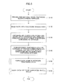
- Fig. 5 schematically illustrates a flow of a method of manufacturing a honeycomb structure according to the present invention.
- the method of manufacturing a honeycomb structure according to the present invention includes:
- Step S150 of (e) and/or step S160 of (f) may be omitted.
- the method of manufacturing a honeycomb structure according to the present invention may have the step of joining multiple honeycomb units by interposing an adhesive layer.
- raw material paste having silicon carbide (SiC) as a principal component is prepared.
- an organic binder Apart from silicon carbide (SiC) particles, an organic binder, a dispersion medium, a molding aid (for example, molding lubricant, molding plasticizer or the like) and the like may be suitably added to the raw material paste.
- a molding aid for example, molding lubricant, molding plasticizer or the like
- the organic binder is not limited in particular, and may be one or more kinds of organic binders selected from, for example, methylcellulose, carboxymethylcellulose, hydroxyethylcellulose, polyethylene glycol, phenolic resin, epoxy resin and the like.
- the amount of the organic binder blended is preferably 1 part by weight to 10 parts by weight to the total of 100 parts by weight of the inorganic particles.
- the dispersion medium is not limited in particular, and may be, for example, water, an organic solvent (such as benzene), alcohol (such as methanol) or the like.
- the molding aid is not limited in particular, and may be, for example, ethylene glycol, dextrin, a fatty acid, fatty acid soap, polyalcohol or the like, where two or more kinds of molding aids may be blended.
- a fatty acid is desirable.
- the fatty acid is preferably an unsaturated fatty acid, and more desirably a higher fatty acid.
- the higher fatty acid desirably has a carbon number more than or equal to 15 and less than 65.
- the raw material paste is not limited to this, and is preferably subjected to mixing and kneading.
- the raw material paste may be mixed using a mixer, an attritor or the like, and may be well kneaded with a kneader or the like.
- a honeycomb molded body is formed by molding the raw material paste prepared in step S110.
- the method of molding a honeycomb molded body is not limited in particular.
- a honeycomb molded body having multiple cells is molded from the raw material paste by extrusion molding or the like.
- the obtained honeycomb molded body is preferably dried.
- the drying apparatus used for drying is not limited in particular, and may be a microwave drying apparatus, a hot air drying apparatus, a dielectric drying apparatus, a reduced-pressure drying apparatus, a vacuum drying apparatus, a freeze drying apparatus or the like.
- the obtained dried honeycomb molded body is preferably degreased.
- the conditions for degreasing which are not limited in particular and are suitably selected in accordance with the kind and amount of the organic matter included in the molded body, are preferably 400 °C and 2 hours in the rough.
- the obtained dried honeycomb molded body is fired (first heat treatment).
- the conditions for firing are not limited in particular. It is preferable to perform firing for 1 hour to 5 hours at 2000 °C to 2200 °C.
- the atmosphere for firing needs to be an inert atmosphere containing no nitrogen, such as an argon atmosphere or the like. This is because if firing is performed in an environment containing nitrogen, a nitrogen component in the environment is captured through gas phase diffusion into sintered silicon carbide particles during the sintering of the silicon carbide particles, which makes it difficult to cause nitrogen to be present only on the surfaces of silicon carbide particles forming cell walls in a honeycomb unit to be finally obtained.
- the honeycomb fired body obtained in step S130 is subjected to heat treatment (second heat treatment).
- This second heat treatment is performed in an environment containing nitrogen.
- the second heat treatment is preferably performed in the temperature range of 1800 °C to 2200 °C, and more preferably, in the range of 1800 °C to 2000 °C.
- the second heat treatment is preferably performed for 2 hours to 8 hours.
- the temperature of the second heat treatment is less than 1800 °C, nitrogen atoms (N) are prevented from diffusing onto the surfaces of the silicon carbide particles, so that formation of a nitrogen-containing layer is prevented. If the temperature of the second heat treatment exceeds 2200 °C, the sintering of the silicon carbide particles progresses. Therefore, nitrogen atoms (N) diffuse into sintered silicon carbide particles through gas phase diffusion, so that nitrogen atoms (N) are prevented from being present only on the surfaces of the silicon carbide particles.
- a silica layer is further formed on the surfaces of the silicon carbide particles of the honeycomb unit obtained in step S140.
- the method of forming a silica layer is not limited in particular.
- the silica layer may be formed by, for example, covering the surface of the nitrogen-containing layer with silicon by adding metal Si (silicon) particles to the surface of the honeycomb unit and oxidizing the metal Si (silicon) by heating the honeycomb unit.
- the method of adding metal Si (silicon) particles to the surface of the honeycomb unit is, for example, immersing the honeycomb unit in molten silicon, or the like.
- the method of oxidizing metal Si (silicon) particles added to the surfaces of the silicon carbide particles of the honeycomb unit is, for example, subjecting the honeycomb unit to heat treatment in an oxidizing atmosphere, or the like.
- the temperature of heat treatment is preferably in the range of 1000 °C to 1400 °C
- the time of heat treatment is preferably in the range of 1 hour to 10 hours.
- the metal Si (silicon) particles are prevented from being sufficiently oxidized, so that a silica layer is prevented from being formed on the surfaces of the silicon carbide particles.
- the temperature of heat treatment exceeds 1400 °C, the metal Si (silicon) particles melt, so that a silica layer is prevented from being formed on the surfaces of the silicon carbide particles.
- the honeycomb unit is provided with a pair of electrodes.
- This process is preferably performed before the above-described step (e) (step S150) after the above-described step (d) (step S140).
- this process may be performed after cutting the silica layer where the electrodes are to be provided after the above-described step (e) (step S150).
- the positions where electrodes are provided are not limited in particular.
- the electrodes are preferably provided one on each end portion of the honeycomb unit entirely around the end portion or at least on the curved side so as to facilitate attachment of terminals and supply of electric current.
- the electrodes are formed of metal or the like. Further, the electrodes may be provided by, for example, metal spraying, metal sputtering, metal vapor deposition or the like.
- the step of causing a catalyst to be supported on the cell walls of the honeycomb unit may be further performed after the above-described step (d) (step S140) or the above-described step (e) (step S150).
- a catalyst is supported on the cell walls of the honeycomb unit.
- platinum, rhodium, palladium or the like may be used as the catalyst.
- the method of causing a catalyst to be supported is not limited in particular.
- the catalyst may be supported by interposing an alumina layer.
- the method of manufacturing a honeycomb structure of the present invention may have the step of joining multiple honeycomb units by interposing an adhesive layer (joining process).
- honeycomb structure of the aggregated structure multiple honeycomb units obtained with the above-described method are joined by interposing an adhesive layer.
- This joining process is performed after the above-described step (d) (step S140).
- the joining process is performed after the above-described step (e) (step S150) if the method of manufacturing a honeycomb structure of the present invention includes the above-described step (e) (step S150) (silica layer forming process).
- the method of manufacturing a honeycomb structure of the present invention includes the above-described step (f) (step S160) (catalyst supporting process)
- the joining process is performed before the above-described step (f) (step S160).
- the method of manufacturing a honeycomb structure of the present invention includes the above-described step (e) (step S150) (silica layer forming process) and the above-described step (f) (step S160) (catalyst supporting process), the joining process is performed between the above-described step (e) (step S150) and the above-described step (f) (step S160).
- a honeycomb unit was manufactured in the following manner, and a change in the electrical resistivity of the honeycomb unit due to temperature was evaluated.
- raw material paste for molding a honeycomb unit was prepared.
- the raw material paste was prepared by mixing 690 g of an organic binder (methylcellulose), 115 g of a molding lubricant (UNILUB), 115 g of a molding plasticizer (glycerin), and 1600 g of ion-exchanged water with 1000 g of silicon carbide particles.
- the obtained raw material paste was subjected to extrusion molding using a screw molding machine, thereby manufacturing a honeycomb molded body of 10 mm square and 50 mm long.
- the cell walls of the honeycomb molded body were 0.2 mm in thickness, and the cell density of the honeycomb molded body was 600 cpsi.
- honeycomb fired body (also referred to as honeycomb unit) has an average porosity of 45% and an average pore size of 11 ⁇ m.
- this honeycomb fired body was subjected to heat treatment at 1900 °C for 8 hours in a nitrogen atmosphere (second heat treatment).
- honeycomb unit thus obtained is referred to as honeycomb unit according to Example 1."
- silicon carbide particles were observed with a voltage of 4 V applied to a probe, and such an image as to allow determination of the variation of carrier concentration was captured.
- FIG. 6 is a result (photograph) of an SNDM observation of the honeycomb unit according to Example 1.
- FIG. 6 shows that a nitrogen-containing layer is formed on the surface (a white portion in the photograph) of a silicon carbide particle of Example 1. Further, one part of the surface of the silicon carbide particle in the photograph of FIG. 6 (the frame part in FIG. 6 ) was selected, and a line analysis was conducted from inside to the surface of the silicon carbide particle.
- FIG. 7 is a chart illustrating the result of the line analysis of a partial surface of the silicon carbide particle in the honeycomb unit according to Example 1.
- the range where there is an increase in carrier concentration is determined as the thickness of the nitrogen-containing layer.
- the interval between points where the second-order differential coefficient of the carrier concentration curve becomes zero is defined as the thickness of the nitrogen--containing layer (indicated by double--headed arrow TH in FIG. 7 ).
- the thickness of the nitrogen-containing layer was 300 nm.
- honeycomb unit according to Example 2 was manufactured in the same manner as in Example 1. In Example 2, however, the honeycomb unit obtained in Example 1 (hereinafter referred to as "honeycomb unit having a nitrogen-containing layer") was further subjected to the following treatment, so that a silica layer was formed on the surfaces of the silicon carbide particles.
- the entire "honeycomb unit having a nitrogen-containing layer" was immersed in a bath of aqueous liquid containing metal Si (silicon) particles, so that the metal Si (silicon) particles were added to the surfaces of the silicon carbide particles.
- this "honeycomb unit having a nitrogen-containing layer” was dried and was thereafter heated at 1200 °C for 1 hour in the atmosphere.
- a silica layer was formed on the surfaces of the silicon carbide particles (technically, the surface of the nitrogen-containing layer).
- the silica layer was 500 nm in thickness.
- the thickness of the nitrogen-containing layer hardly changed through this heat treatment, and was 300 nm.
- the thickness of the silica layer was measured with a transmission electron microscope.
- a honeycomb unit according to Comparative Example 1 was manufactured in the same manner as in Example 1. In Comparative Example 1, however, the "first heat treatment” was performed at 2200 °C for 3 hours in a nitrogen atmosphere. Further, the “second heat treatment” was not performed in Comparative Example 1.
- Example 1 The configurations (the presence or absence of a nitrogen-containing layer and the presence or absence of a silica layer) of the honeycomb units according to Example 1, Example 2, and Comparative Example 1 are collectively illustrated in Table 1.
- Table 1 NITROGEN-CONTAINING LAYER SILICA LAYER EVALUATION OF TEMPERATURE DEPENDENCE OF ELECTRICAL RESISTIVITY EVALUATION OF CHANGE IN ELECTRICAL RESISTIVITY OVER TIME IN ACCELERATED ENVIRONMENT EXAMPLE 1 YES (300nm) NO LOW TEMPERATURE DEPENDENCE SHARP CHANGE EXAMPLE 2 YES (300nm) YES (500nm) LOW TEMPERATURE DEPENDENCE NO SUBSTANTIAL CHANGE COMPARATIVE EXAMPLE 1 NO NO HIGH TEMPERATURE DEPENDENCE -
- Example 1 The following evaluation of a change in electrical resistivity due to temperature was performed using the honeycomb units of Example 1, Example 2, and Comparative Example 1 manufactured in the above-described manner.
- a change in the electrical resistivity of each honeycomb unit due to temperature was measured. The measurement was performed through the following steps.
- silver paste was applied entirely around each end portion (10 mm in width) of each of the honeycomb units of Example 1 and Comparative Example 1 as electrodes. Further, a platinum line was connected to each of the electrodes.
- Example 2 the silica layer was cut off entirely around each end portion (10 mm in width) of the honeycomb unit of Example 2 using sandpaper, and thereafter, silver paste was applied as electrodes to where the silica layer had been cut off. Further, in Example 2 as well, a platinum line was connected to each of the electrodes the same as in Example 1 and Comparative Example 1.
- evaluation samples samples for evaluating a change in electrical resistivity due to temperature with respect to Example 1, Example 2, and Comparative Example 1 (hereinafter referred to as evaluation samples) were manufactured.
- a constant-voltage power supply unit was connected between the electrodes of each of the evaluation samples, and a voltage of 200 V was applied between the electrodes. In this state, the electrical resistivities of the evaluation samples were measured. Thereafter, the evaluation samples were heated to temperatures (up to 550 °C), and the electrical resistivities of the evaluation samples were measured in the same manner.
- FIG. 8 is a graph illustrating changes in the electrical resistivities of the honeycomb units according to Example 1 and Comparative Example 1 due to temperature.
- This graph of FIG. 8 shows that the electrical resistivity of the honeycomb unit according to Comparative Example 1 tends to drop sharply from an electrical resistivity of 1.8 ⁇ cm at 25 °C to an electrical resistivity of 0.3 ⁇ cm at 500 °C with an increase in temperature (from 25 °C to 500 °C).
- the temperature dependence of the electrical resistivity is controlled, and in the temperature range of room temperature (25 °C) to 550 °C, the electrical resistivity is 32.8 ⁇ cm at 25 °C and 11.2 ⁇ cm at 500 °C, thus showing that a decrease in electrical resistivity is controlled.
- the measurement was performed at 1000 °C in the atmosphere, and the electrical resistivity was measured for up to 100 hours.
- FIG. 9 is a graph illustrating changes in electrical resistivity over time at 1000 °C in the atmosphere in the honeycomb units according to Example 1 and Example 2.
- the electrical resistivity increased sharply from 125 ⁇ cm to 31200 ⁇ cm in 10 hours.
- the electrical resistivity hardly changes up to at least 100 hours later. This suggests that in the case of forming a silica layer on the nitrogen-containing layer, the silica layer serves as a protection layer to improve the oxidation resistance of the nitrogen-containing layer.
- the durability of the nitrogen-containing layer is believed to be further improved by further forming a silica layer on the nitrogen-containing layer. Further, this makes it possible to control the temperature dependence of electrical resistivity over a long period of time.
- Example 1 The electrical resistivity of Example 1 in the accelerated environment presents a sharp change.
- the accelerated environment implemented in this test has severe conditions of high temperature and high oxygen concentration compared with those of a practical usage environment. Therefore, even the configuration of Example 1 is sufficiently usable for practical applications.
Landscapes
- Chemical & Material Sciences (AREA)
- Engineering & Computer Science (AREA)
- Ceramic Engineering (AREA)
- Manufacturing & Machinery (AREA)
- Structural Engineering (AREA)
- Organic Chemistry (AREA)
- Materials Engineering (AREA)
- Inorganic Chemistry (AREA)
- Chemical Kinetics & Catalysis (AREA)
- Combustion & Propulsion (AREA)
- Mechanical Engineering (AREA)
- General Engineering & Computer Science (AREA)
- Catalysts (AREA)
- Exhaust Gas Treatment By Means Of Catalyst (AREA)
Abstract
Description
- The present invention relates to a honeycomb structure that treats exhaust gas and a method of manufacturing a honeycomb structure.
- A large number of techniques have been developed in relation to conversion of exhaust gas of automobiles or the like. With an increase in traffic, however, countermeasures taken against exhaust gas have hardly been satisfactory. Not only in Japan but also globally, is emission control of automobiles or the like going to be further tightened.
- In order to meet such control of exhaust gas, catalyst supports capable of treating predetermined toxic components contained in exhaust gas are used in exhaust gas converting systems. Further, a honeycomb structure is known as a member for such catalyst supports.
- This honeycomb structure has, for example, multiple cells (through holes) extending from one end face to another end face of the honeycomb structure along its longitudinal directions, and these cells are separated from each other by cell walls on which a catalyst is supported. Accordingly, in the case of causing exhaust gas to flow through such a honeycomb structure, substances contained in the exhaust gas, such as HC (a hydrocarbon compound), CO (carbon monoxide), and NOx (nitrogen oxides), are converted (oxidized or reduced) by the catalyst supported on the cell walls, so that these toxic components in the exhaust gas may be treated.
- In general, the cell walls (base material) of such a honeycomb structure are formed of cordierite. Further, a catalyst support layer of γ-alumina is formed on the cell walls, and a noble metal catalyst such as platinum and/or rhodium is supported on this catalyst support layer.
- Further, a technique has been proposed that, in order to improve conversion performance at exhaust gas temperatures lower than a temperature at which a catalyst becomes active, uses a honeycomb structure of a relatively low electrical resistance, provides this honeycomb structure with electrodes for applying voltage, and supplies the honeycomb structure with electric current, thereby causing the honeycomb structure to perform self-heating (Patent Document 1).
- For example,
Patent Document 1 discloses that by adding silicon carbide particles and particles of a compound containing nitride to raw material in manufacturing a silicon-carbide-based honeycomb structure, it is possible to reduce the electrical resistivity of a honeycomb structure to be finally obtained. - [Patent Document 1] Japanese Laid-Open Patent Application No.
7-80226 - According to the conventional honeycomb structure described in
Patent Document 1, the finally obtained honeycomb structure can be reduced in electrical resistivity. Therefore, by supplying the honeycomb structure with electric current via a pair of electrodes, it is possible to subject the honeycomb structure to resistance heating. - In general, however, the electrical resistivity of a resistor is a function of temperature and tends to change with an increase in temperature. Accordingly, in the conventional honeycomb structure described in
Patent Document 1 as well, the electrical resistivity is believed to change with temperature and, in particular, to decrease sharply with an increase in temperature. - On the other hand, in the case of using a honeycomb structure as an exhaust gas converting apparatus, the temperature of the honeycomb structure varies in a wide range from room temperature (for example, 25 °C) to approximately 500 °C. Accordingly, even if the honeycomb structure has an electrical resistivity in an appropriate range in a certain temperature region, a change in the temperature of the honeycomb structure causes a change in the electrical resistivity, so that the electrical resistivity goes out of the appropriate range. Specifically, if a honeycomb structure has an electrical resistivity in an appropriate range in a certain temperature region, an increase in the temperature of the honeycomb structure causes a decrease in the electrical resistivity. As a result, the electrical resistivity goes out of the appropriate range, thus causing a problem in that it is difficult to properly heat the honeycomb structure.
- The present invention has been made in view of such a problem, and has an object of providing a honeycomb structure in which the temperature change dependence of electrical resistivity is controlled. Further, the present invention has an object of providing a method of manufacturing such a honeycomb structure.
- According to the present invention, a honeycomb structure is provided that includes a pillar-shaped honeycomb unit having cells defined by cell walls, wherein the cell walls contain silicon carbide particles, and a nitrogen-containing layer is formed on surfaces of the silicon carbide particles.
- Here, in the honeycomb structure according to the present invention, the nitrogen-containing layer may have a thickness in a range of 100 nm to 600 nm.
- Here, in the honeycomb structure according to the present invention, a silica layer may be formed on a surface of the nitrogen-containing layer.
- Further, in the honeycomb structure according to the present invention, the silica layer may have a thickness in a range of 100 nm to 800 nm.
- Further, in the honeycomb structure according to the present invention, a catalyst may be supported on the cell walls.
- Further, in the honeycomb structure according to the present invention, the catalyst may be one of platinum, rhodium, and palladium, and the catalyst may be supported on the cell walls by interposing an alumina layer.
- Further, the honeycomb structure according to the present invention may have a plurality of the honeycomb units joined by interposing an adhesive layer.
- In addition, according to the present invention, a method of manufacturing a honeycomb structure is provided that includes the steps of (a) preparing paste containing silicon carbide particles; (b) forming a honeycomb molded body by molding the paste; (c) obtaining a pillar-shaped honeycomb unit having cells defined by cell walls by firing the honeycomb molded body in an inert atmosphere containing no nitrogen; and (d) forming a nitrogen-containing layer on surfaces of the silicon carbide particles forming the cell walls by heating the honeycomb unit in an environment containing nitrogen.
- Here, in the method of manufacturing a honeycomb structure according to the present invention, step (d) may be performed at a temperature in a range of 1800 °C to 2200 °C.
- Further, in the method of manufacturing a honeycomb structure according to the present invention, the nitrogen-containing layer may have a thickness in a range of 100 nm to 600 nm.
- In addition, the method of manufacturing a honeycomb structure according to the present invention may further include the step of (e) forming a silica layer on a surface of the nitrogen-containing layer after step (d).
- In this case, step (e) may include subjecting the honeycomb unit to heat treatment at a temperature of 1000 °C to 1400 °C in an atmosphere containing oxygen after coating the surface of the nitrogen-containing layer with silicon.
- Further, the silica layer may have a thickness in a range of 100 nm to 800 nm.
- In addition, the method of manufacturing a honeycomb structure according to the present invention may further include the step of (f) causing a catalyst to be supported on the cell walls after step (d).
- Alternatively, the method of manufacturing a honeycomb structure according to the present invention may further include the step of (f) causing a catalyst to be supported on the cell walls after steps (d) and (e).
- In addition, the method of manufacturing a honeycomb structure according to the present invention may further include the step of joining a plurality of the honeycomb units by interposing an adhesive layer.
- According to the present invention, it is possible to provide a honeycomb structure in which the temperature change dependence of electrical resistivity is controlled. Further, it is possible to provide a method of manufacturing such a honeycomb structure.
-
-
FIG. 1 is a schematic perspective view of a honeycomb structure of the present invention. -
FIGS. 2A and 2B are graphs schematically illustrating energy levels of silicon carbide and nitrogen, whereFIG. 2A illustrates the general energy levels of silicon carbide molecules and nitrogen atoms in the case where the concentration of nitrogen atoms is low andFIG. 2B illustrates the general energy levels of silicon carbide molecules and nitrogen atoms in the case where the concentration of nitrogen atoms is high. -
FIG. 3 is a schematic perspective view of another honeycomb structure according to the present invention. -
FIG. 4 is a schematic perspective view of a honeycomb unit that is a component of the honeycomb structure ofFIG. 3 . -
FIG. 5 is a flowchart schematically illustrating a method of manufacturing a honeycomb structure of the present invention. -
FIG. 6 is a result (photograph) of an SNDM observation of a honeycomb unit according to Example 1. -
FIG. 7 is a chart illustrating the result of a line analysis of a partial surface of a silicon carbide particle in the honeycomb unit according to Example 1. -
FIG. 8 is a graph illustrating changes in electrical resistivity due to temperature in the honeycomb unit according to Example 1 and a honeycomb unit according to Comparative Example 1. -
FIG. 9 is a graph illustrating changes in electrical resistivity over time at 1000 °C in the atmosphere in the honeycomb unit according to Example 1 and a honeycomb unit according to Example 2. - A description is given below, with reference to the drawings, of the present invention.
-
FIG. 1 schematically illustrates ahoneycomb structure 100 according to the present invention. - As illustrated in
FIG. 1 , thehoneycomb structure 100 of the present invention includes asingle honeycomb unit 130 defined by twoopen end faces side surface 120. - The
honeycomb unit 130 includes multiple cells (through holes) 122 andcell walls 124 defining thecells 122. Thecells 122 extend from theend face 110A to theend face 110B along the longitudinal directions of thehoneycomb unit 130 to be open at the end faces 110A and 110B. - The
honeycomb unit 130 is formed of, for example, a material having silicon carbide (SiC) as a principal component. Thehoneycomb unit 130 contains a resistance adjusting component in order to reduce electrical resistivity. The resistance adjusting component is nitrogen atoms (N) with which the silicon carbide is doped. That is, thecell walls 124 of thehoneycomb unit 130 contains silicon carbide, and a nitrogen-containing layer is formed on the surface of the silicon carbide. A catalyst is supported on thecell walls 124 of thehoneycomb unit 130. - Further, in the case of
FIG. 1 , thehoneycomb structure 100 includes a pair ofelectrodes - The
first electrode 160A is provided entirely around afirst end part 115A of thehoneycomb unit 130. Thesecond electrode 160B is provided entirely around asecond end part 115B of thehoneycomb unit 130. However, the positions where theseelectrodes electrodes honeycomb structure 100. - The
honeycomb structure 100 may be subjected to resistance heating by externally applying voltage between theelectrodes honeycomb structure 100 thus configured. - Here, for example, in the conventional honeycomb structure of a resistance heating type described in
Patent Document 1, a compound having a low specific resistance value is added to raw material containing silicon carbide particles in order to reduce the electrical resistivity of the honeycomb structure. In this case, a component (low resistance component) contained in the added compound is evenly diffused in the silicon carbide particles during the firing of the raw material, so that it is possible to dispose the low resistance component throughout cell walls in a honeycomb unit to be finally obtained. This makes it possible to reduce the electrical resistivity of the honeycomb unit. - In general, however, the electrical resistivity of a resistor is a function of temperature and tends to change with an increase in temperature. Accordingly, in the conventional honeycomb structure described in
Patent Document 1 as well, the electrical resistivity is believed to change with temperature and, in particular, to decrease sharply with an increase in temperature. - On the other hand, in the case of using a honeycomb structure as an exhaust gas converting apparatus, the temperature of the honeycomb structure varies in a wide range from room temperature (for example, 25 °C) to approximately 500 °C. Accordingly, even if the honeycomb structure has an electrical resistivity in an appropriate range in a certain temperature region, a change in the temperature of the honeycomb structure causes a change in the electrical resistivity, so that the electrical resistivity goes out of the appropriate range. Specifically, if a honeycomb structure has an electrical resistivity in an appropriate range in a certain temperature region, an increase in the temperature of the honeycomb structure causes a decrease in the electrical resistivity. As a result, the electrical resistivity goes out of the appropriate range, thus causing a problem in that it is difficult to properly heat the honeycomb structure.
- On the other hand, in the
honeycomb structure 100 according to the present invention, a layer containing nitrogen atoms (hereinafter referred to as "nitrogen-containing layer") is present on the surfaces of silicon carbide particles that form thecell walls 124. That is, according to the present invention, nitrogen atoms that contribute to the electrical resistivity of a honeycomb unit are present in a concentrated state on the surfaces of silicon carbide particles, so that inside the silicon carbide particles, the nitrogen atoms are absent or present at a lower concentration than on the surfaces of the silicon carbide particles. - By thus disposing nitrogen atoms in a concentrated state on the surfaces of silicon carbide particles, it is possible to control the temperature dependence of the electrical resistivity of a honeycomb unit.
-
FIGS. 2A and 2B are graphs for illustrating a principle considered to be the reason why the temperature dependence of the electrical resistivity of a honeycomb unit is controlled in the present invention. -
FIG. 2A illustrates the general energy levels of silicon carbide molecules and nitrogen atoms in the case where the concentration of nitrogen atoms is low.FIG. 2B illustrates the general energy levels of silicon carbide molecules and nitrogen atoms in the case where the concentration of nitrogen atoms is high. - In
FIGS. 2A and 2B , the density of states (cm-3) represents the density of electrons or holes present at a certain energy level, the valence band represents an energy band filled with valence electrons, and the conduction band represents an energy band where there are electrons that can move freely as carriers. - As illustrated in
FIG. 2A , in the case where the concentration of nitrogen atoms is low, the donor level of nitrogen atoms (approximately 0.05 eV) is believed to be present between the valence band of silicon carbide molecules and the conduction band. In this case, in order for the electrons of nitrogen atoms at the donor level to be excited to the conduction band, corresponding activation energy is required. Usually, this activation energy is a function of temperature. Therefore, the behavior of excitation of electrons to the conduction band presents significant temperature dependence. Therefore, in a honeycomb unit where nitrogen atoms of a small amount are evenly distributed, the electrical resistivity is caused to have conspicuous temperature dependence. - On the other hand, in the case where the concentration of nitrogen atoms is high, a donor band is formed instead of the donor level. Further, as illustrated in
FIG. 2B , this donor band overlaps the conduction band of silicon carbide molecules. Accordingly, in this case, the excitation energy for excitation from the donor band to the conduction band is sufficiently reduced, so that the temperature dependence of the activation energy is reduced. - The donor level represents the energy level of electrons present in a band gap, and the donor band represents a group of electron orbits formed by the density of a large number of electrons present at the donor level in the band gap.
- According to the present invention, a "nitrogen-containing layer" is present on the surfaces of silicon carbide particles, that is, nitrogen atoms are concentrated on the surfaces of silicon carbide particles. It is believed that this causes the energy state of nitrogen to be as illustrated in
FIG. 2B so that the temperature dependence of the electrical resistivity of a honeycomb unit is controlled. - This principle has been thought out by the inventor of the present invention based on the present knowledge, and it is to be noted that the temperature dependence of the electrical resistivity of a honeycomb unit may also be controlled for other reasons in a configuration of the present invention.
- Further, the presence of such a nitrogen-containing layer may be determined by scanning nonlinear dielectric microscopy (SNDM).
- SNDM, which is one of the measurement methods based on scanning probe microscopy (SPM), is a technique that measures a change in polarity and a concentration distribution of carriers on the surface of a sample based on the charge sign of a probe and the magnitude of an electric field caused upon application of voltage to the probe brought close to the surface of the sample. SNDM is used in, for example, the measurement of a concentration distribution of semiconductor carriers, etc.
- Here, according to the present invention, the thickness of the nitrogen-containing layer is, for example, in the range of 100 nm to 600 nm, preferably in the range of 200 nm to 600 nm, and more preferably, in the range of 200 nm to 400 nm.
- If the thickness of the nitrogen-containing layer is less than 100 nm, the electrical resistivity of a honeycomb unit is not sufficiently reduced. As a result, the amount of electric conduction between electrodes is reduced, so that the honeycomb unit is prevented from being heated to an appropriate temperature. On the other hand, if the thickness of the nitrogen-containing layer exceeds 600 nm, the electrical resistivity of a honeycomb unit is caused to have temperature dependence, so that the electrical resistivity of the honeycomb unit decreases at the time of high temperatures in particular. Therefore, the honeycomb unit is prevented from being heated to an appropriate temperature.
- The nitrogen-containing layer is oxidized by long-term use at high temperatures. Progress in the oxidation of the nitrogen-containing layer impairs the control effect of the nitrogen-containing layer on the temperature dependence of electrical resistivity.
- In order to address this problem, it is preferable to provide a silica layer as a protection layer on the surface of the nitrogen-containing layer. This silica layer improves the long-term stability of the nitrogen-containing layer and makes it possible to maintain the control effect on the temperature dependence of electrical resistivity over a long period of time.
- The thickness of the silica layer is, for example, in the range of 100 nm to 800 nm, preferably in the range of 100 nm to 500 nm, and more preferably, in the range of 200 nm to 500 nm.
- If the thickness of the silica layer is less than 100 nm, it is difficult to sufficiently prevent oxidation of the nitrogen-containing layer, so that the oxidation of the nitrogen-containing layer progresses. On the other hand, if the thickness of the silica layer exceeds 800 nm, a stress due to a difference in the coefficient of thermal expansion between the silica layer and the silicon carbide particles increases, so that the silica layer peels off the silicon carbide particles. As a result, the temperature dependence of electrical resistivity is less likely to be controlled.
- It is possible to form such a silica layer easily by, for example, adding metal Si (silicon) particles to the surfaces of the silicon carbide particles of the cell walls of a honeycomb unit and thereafter oxidizing the metal Si (silicon) by heating the honeycomb unit.
-
FIG. 3 is a schematic perspective view of another honeycomb structure according to the present invention. - The
honeycomb structure 100 illustrated inFIG. 1 is a so-called "monolithic structure" type formed of a single honeycomb unit. The present invention, however, may also be applied to a honeycomb structure having a so-called "aggregated structure" formed of multiple honeycomb units. -
FIG. 3 illustrates ahoneycomb structure 200 of the "aggregated structure" according to the present invention. Further,FIG. 4 illustrates a typical honeycomb unit that is a component of thehoneycomb structure 200 illustrated inFIG. 3 . - As illustrated in
FIG. 3 , thehoneycomb structure 200 of the present invention has two open end faces 210A and 210B and aside surface 220. - The
honeycomb structure 200 is formed by joining multiple honeycomb units by interposing anadhesive layer 250. For example, in the case illustrated inFIG. 3 , thehoneycomb structure 200 includes fourhoneycomb units 230A through 230D. Thehoneycomb units 230A through 230D are formed of a material having silicon carbide (SiC) as a principal component. - However, the
honeycomb units 230A through 230D contain a resistance adjusting component in order to reduce electrical resistivity. The resistance adjusting component is nitrogen atoms (N) with which the silicon carbide is doped. - As illustrated in
FIG. 4 , thehoneycomb unit 230A has a pillar structure having end faces 214A and 214B having a sectorial shape of a quarter circle and threesides side 217A and theside 218A have a flat surface, and theside 219A is a side having a curved surface (hereinafter referred to as "curved side"). - In the case of
FIG. 3 , thehoneycomb units 230B through 230D have the same shape as thehoneycomb unit 230A. For example, as illustrated inFIG. 3 , thehoneycomb unit 230B has acurved side 219B corresponding to thecurved side 219A of thehoneycomb unit 230A. - The
honeycomb unit 230A includesmultiple cells 222 andcell walls 224 defining thecells 222. Thecells 222 extend from theend face 214A to theend face 214B along the longitudinal directions of thehoneycomb unit 230A to be open at the end faces 214A and 214B. A catalyst is supported on thecell walls 224 of thehoneycomb unit 230A. - As described above, the
cell walls 224 of thehoneycomb unit 230A are formed of silicon carbide particles, and a nitrogen-containing layer is formed on the surfaces of the silicon carbide particles. A silica layer may be formed on the surface of the nitrogen-containing layer. - It is clear to a person having ordinary skill in the art that the above-described effects according to the present invention are also produced by the
honeycomb structure 200 including thishoneycomb unit 230A. - A pair of electrodes is not illustrated in the
honeycomb structure 200 illustrated inFIG. 3 . However, it is clear to a person having ordinary skill in the art that thehoneycomb structure 200 may have a pair of electrodes the same as in the case ofFIG. 1 . In this case, for example, the electrodes are provided one on each end portion of each of the curved sides (of which thecurved sides FIG. 3 ) of thehoneycomb units 230A through 230D of thehoneycomb structure 200. - Next, a description is given in more detail of a configuration of each of members of a honeycomb structure according to the present invention. In the following, a description is given principally of members of the
honeycomb structure 200 having the aggregated structure illustrated inFIG. 3 . However, it is clear to a person having ordinary skill in the art that part of this description may also be applied to thehoneycomb structure 100 having the monolithic structure illustrated inFIG. 1 . Further, inFIG. 3 , theconductive honeycomb units 230A through 230D have the same configuration. Accordingly, theconductive honeycomb unit 230A is taken here, and a description is given of its configuration. - The
honeycomb unit 230A is formed of an inorganic material based on silicon carbide (SiC), and contains, as a resistance adjusting component, nitrogen atoms (N) with which the silicon carbide (SiC) is doped. - The cross-sectional shape of the
honeycomb unit 230A perpendicular to its longitudinal directions is not limited in particular, and may be any shape such as a square shape, a rectangular shape, a hexagonal shape or the like. - Further, the cross-sectional shape of the
cells 222 of thehoneycomb unit 230A perpendicular to its longitudinal directions is not limited in particular, and may be, for example, a triangular shape, a polygonal shape or the like in addition to a square shape. - The cell density of the
honeycomb unit 230A is preferably 15.5 cells/cm2 to 186 cells/cm2 (100 cpsi to 1200 cpsi), more preferably 31 cells/cm2 to 155 cells/cm2 (200 cpsi to 1000 cpsi), and still more preferably 46.5 cells/cm2 to 124 cells/cm2 (300 cpsi to 800 cpsi). - If the cell density of the
honeycomb unit 230A is less than 15.5 cells/cm2, thecell walls 224 have a reduced area of contact with exhaust gas, so that sufficient conversion performance is prevented from being obtained. On the other hand, if the cell density of thehoneycomb unit 230A exceeds 186 cells/cm2, the pressure of a honeycomb structure increases. - The porosity of the
honeycomb unit 230A may be in the range of 15% to 50%. - If the porosity of the
honeycomb unit 230A is less than 15%, the elastic modulus of thehoneycomb unit 230A increases, so that thehoneycomb unit 230A is likely to be broken because of a stress generated at the time of its energization. On the other hand, if the porosity of thehoneycomb unit 230A exceeds 50%, the strength of thecell walls 224 of thehoneycomb unit 230A is reduced. - The thickness of the
cell walls 224 of thehoneycomb unit 230A is not limited in particular. However, a desirable lower limit is 0.05 mm in terms of strength, and a desirable upper limit is 0.3 mm in terms of conversion performance. - The catalyst supported on the
cell walls 224 of thehoneycomb unit 230A is not limited in particular, and may be, for example, platinum, rhodium, palladium or the like. The catalyst may be supported on thecell walls 224 by interposing an aluminum layer. - The
adhesive layer 250 of thehoneycomb structure 200 is formed using adhesive layer paste as raw material. The adhesive layer paste may contain inorganic particles, an inorganic binder, inorganic fibers, and/or an organic binder. - Silicon carbide (SiC) is desirable as inorganic particles of the adhesive layer paste. Inorganic sol, a clay-based binder or the like may be used as the inorganic binder. Examples of the inorganic sol include alumina sol, silica sol, titania sol, water glass and the like. Examples of the clay-based binder include clay, kaolin, montmonrillonite, sepiolite, attapulgite and the like. These may be used alone or in combination. Alumina, silica, silicon carbide, silica-alumina, glass, potassium titanate, aluminum borate or the like is preferable as the material of the inorganic fibers. These may be used alone or in combination. Of the above-described materials of the inorganic fibers, silica-alumina is desirable.
- The organic binder is not limited in particular, and is, for example, one or more selected from polyvinyl alcohol, methylcellulose, ethylcellulose, carboxymethylcellulose and the like. Of the organic binders, carboxymethylcellulose is desirable.
- The thickness of the
adhesive layer 250 is preferably in the range of 0.3 mm to 2 mm. If the thickness of theadhesive layer 250 is less than 0.3 mm, the joining strength of honeycomb units is not sufficient. If the thickness of theadhesive layer 250 exceeds 2 mm, there is the problem of an increase in the pressure loss of the honeycomb structure. The number of honeycomb units to be joined is suitably determined in accordance with the size of the honeycomb structure. - A honeycomb structure according to the present invention may have any shape. For example, in addition to a circular-pillar shape illustrated in
FIG. 1 andFIG. 3 , the honeycomb structure may also have a cylindroid shape, a square pillar shape, a polygonal pillar shape and the like. - Next, a description is given of a method of manufacturing a honeycomb structure according to the present invention. The following description is given, taking the case of manufacturing the
honeycomb structure 100 illustrated inFIG. 1 as an example. However, thehoneycomb structure 200 illustrated inFIG. 3 may also be manufactured using the same method. -
Fig. 5 schematically illustrates a flow of a method of manufacturing a honeycomb structure according to the present invention. The method of manufacturing a honeycomb structure according to the present invention includes: - (a) the step of preparing paste containing silicon carbide particles (step S110);
- (b) the step of forming a honeycomb molded body by molding the paste (step S120);
- (c) the step of obtaining a pillar-shaped honeycomb unit having cells defined by cell walls by firing the molded body in an inert atmosphere containing no nitrogen (step S130);
- (d) the step of forming a nitrogen-containing layer on the surfaces of the silicon carbide particles forming the cell walls by heating the honeycomb unit in an environment containing nitrogen (step S140);
- (e) the step of forming a silica layer on the nitrogen-containing layer (step 3150); and
- (f) the step of causing a catalyst to be supported on the cell walls (step S160).
- Step S150 of (e) and/or step S160 of (f) may be omitted.
- Further, the method of manufacturing a honeycomb structure according to the present invention may have the step of joining multiple honeycomb units by interposing an adhesive layer.
- A description is given below of each of the steps.
- First, raw material paste having silicon carbide (SiC) as a principal component is prepared.
- Apart from silicon carbide (SiC) particles, an organic binder, a dispersion medium, a molding aid (for example, molding lubricant, molding plasticizer or the like) and the like may be suitably added to the raw material paste.
- The organic binder is not limited in particular, and may be one or more kinds of organic binders selected from, for example, methylcellulose, carboxymethylcellulose, hydroxyethylcellulose, polyethylene glycol, phenolic resin, epoxy resin and the like. The amount of the organic binder blended is preferably 1 part by weight to 10 parts by weight to the total of 100 parts by weight of the inorganic particles.
- The dispersion medium is not limited in particular, and may be, for example, water, an organic solvent (such as benzene), alcohol (such as methanol) or the like.
- The molding aid is not limited in particular, and may be, for example, ethylene glycol, dextrin, a fatty acid, fatty acid soap, polyalcohol or the like, where two or more kinds of molding aids may be blended. Of these molding aids, a fatty acid is desirable. Further, the fatty acid is preferably an unsaturated fatty acid, and more desirably a higher fatty acid. The higher fatty acid desirably has a carbon number more than or equal to 15 and less than 65.
- The raw material paste is not limited to this, and is preferably subjected to mixing and kneading. For example, the raw material paste may be mixed using a mixer, an attritor or the like, and may be well kneaded with a kneader or the like.
- Next, a honeycomb molded body is formed by molding the raw material paste prepared in step S110.
- The method of molding a honeycomb molded body is not limited in particular. For example, a honeycomb molded body having multiple cells is molded from the raw material paste by extrusion molding or the like.
- Thereafter, the obtained honeycomb molded body is preferably dried. The drying apparatus used for drying is not limited in particular, and may be a microwave drying apparatus, a hot air drying apparatus, a dielectric drying apparatus, a reduced-pressure drying apparatus, a vacuum drying apparatus, a freeze drying apparatus or the like. Further, the obtained dried honeycomb molded body is preferably degreased. The conditions for degreasing, which are not limited in particular and are suitably selected in accordance with the kind and amount of the organic matter included in the molded body, are preferably 400 °C and 2 hours in the rough.
- Next, the obtained dried honeycomb molded body is fired (first heat treatment). The conditions for firing are not limited in particular. It is preferable to perform firing for 1 hour to 5 hours at 2000 °C to 2200 °C.
- The atmosphere for firing needs to be an inert atmosphere containing no nitrogen, such as an argon atmosphere or the like. This is because if firing is performed in an environment containing nitrogen, a nitrogen component in the environment is captured through gas phase diffusion into sintered silicon carbide particles during the sintering of the silicon carbide particles, which makes it difficult to cause nitrogen to be present only on the surfaces of silicon carbide particles forming cell walls in a honeycomb unit to be finally obtained.
- Next, in order to form a nitrogen-containing layer on the surfaces of the silicon carbide particles, the honeycomb fired body obtained in step S130 is subjected to heat treatment (second heat treatment).
- This second heat treatment is performed in an environment containing nitrogen. The second heat treatment is preferably performed in the temperature range of 1800 °C to 2200 °C, and more preferably, in the range of 1800 °C to 2000 °C. The second heat treatment is preferably performed for 2 hours to 8 hours.
- If the temperature of the second heat treatment is less than 1800 °C, nitrogen atoms (N) are prevented from diffusing onto the surfaces of the silicon carbide particles, so that formation of a nitrogen-containing layer is prevented. If the temperature of the second heat treatment exceeds 2200 °C, the sintering of the silicon carbide particles progresses. Therefore, nitrogen atoms (N) diffuse into sintered silicon carbide particles through gas phase diffusion, so that nitrogen atoms (N) are prevented from being present only on the surfaces of the silicon carbide particles.
- Through the above-described processes, it is possible to obtain a honeycomb unit having a nitrogen-containing layer on the surfaces of silicon carbide particles.
- Next, if needed, a silica layer is further formed on the surfaces of the silicon carbide particles of the honeycomb unit obtained in step S140.
- The method of forming a silica layer is not limited in particular. The silica layer may be formed by, for example, covering the surface of the nitrogen-containing layer with silicon by adding metal Si (silicon) particles to the surface of the honeycomb unit and oxidizing the metal Si (silicon) by heating the honeycomb unit.
- The method of adding metal Si (silicon) particles to the surface of the honeycomb unit is, for example, immersing the honeycomb unit in molten silicon, or the like. Further, the method of oxidizing metal Si (silicon) particles added to the surfaces of the silicon carbide particles of the honeycomb unit is, for example, subjecting the honeycomb unit to heat treatment in an oxidizing atmosphere, or the like. In this case, the temperature of heat treatment is preferably in the range of 1000 °C to 1400 °C, and the time of heat treatment is preferably in the range of 1 hour to 10 hours.
- If the temperature of heat treatment is less than 1000 °C, the metal Si (silicon) particles are prevented from being sufficiently oxidized, so that a silica layer is prevented from being formed on the surfaces of the silicon carbide particles. On the other hand, if the temperature of heat treatment exceeds 1400 °C, the metal Si (silicon) particles melt, so that a silica layer is prevented from being formed on the surfaces of the silicon carbide particles.
- Through the above-described process, it is possible to manufacture a honeycomb unit having a silica layer further formed on the nitrogen-containing layer.
- In the case of using the honeycomb unit as a honeycomb structure of a resistance heating type, the honeycomb unit is provided with a pair of electrodes. This process is preferably performed before the above-described step (e) (step S150) after the above-described step (d) (step S140). Alternatively, this process may be performed after cutting the silica layer where the electrodes are to be provided after the above-described step (e) (step S150).
- The positions where electrodes are provided are not limited in particular. The electrodes are preferably provided one on each end portion of the honeycomb unit entirely around the end portion or at least on the curved side so as to facilitate attachment of terminals and supply of electric current.
- The electrodes are formed of metal or the like. Further, the electrodes may be provided by, for example, metal spraying, metal sputtering, metal vapor deposition or the like.
- In the method of manufacturing a honeycomb structure of the present invention, the step of causing a catalyst to be supported on the cell walls of the honeycomb unit may be further performed after the above-described step (d) (step S140) or the above-described step (e) (step S150).
- In particular, in the case of using the honeycomb unit as a honeycomb structure for a catalyst support, a catalyst is supported on the cell walls of the honeycomb unit.
- For example, platinum, rhodium, palladium or the like may be used as the catalyst. The method of causing a catalyst to be supported is not limited in particular. The catalyst may be supported by interposing an alumina layer.
- The method of manufacturing a honeycomb structure of the present invention may have the step of joining multiple honeycomb units by interposing an adhesive layer (joining process).
- For example, in the case of manufacturing a honeycomb structure of the aggregated structure, multiple honeycomb units obtained with the above-described method are joined by interposing an adhesive layer.
- This joining process is performed after the above-described step (d) (step S140). In particular, considering the heat resistance of the inorganic fibers contained in the adhesive layer, the joining process is performed after the above-described step (e) (step S150) if the method of manufacturing a honeycomb structure of the present invention includes the above-described step (e) (step S150) (silica layer forming process). Further, if the method of manufacturing a honeycomb structure of the present invention includes the above-described step (f) (step S160) (catalyst supporting process), the joining process is performed before the above-described step (f) (step S160). Further, if the method of manufacturing a honeycomb structure of the present invention includes the above-described step (e) (step S150) (silica layer forming process) and the above-described step (f) (step S160) (catalyst supporting process), the joining process is performed between the above-described step (e) (step S150) and the above-described step (f) (step S160).
- Next, a description is given of examples according to the present invention.
- A honeycomb unit was manufactured in the following manner, and a change in the electrical resistivity of the honeycomb unit due to temperature was evaluated.
- First, raw material paste for molding a honeycomb unit was prepared. The raw material paste was prepared by mixing 690 g of an organic binder (methylcellulose), 115 g of a molding lubricant (UNILUB), 115 g of a molding plasticizer (glycerin), and 1600 g of ion-exchanged water with 1000 g of silicon carbide particles.
- Next, the obtained raw material paste was subjected to extrusion molding using a screw molding machine, thereby manufacturing a honeycomb molded body of 10 mm square and 50 mm long. The cell walls of the honeycomb molded body were 0.2 mm in thickness, and the cell density of the honeycomb molded body was 600 cpsi.
- Next, the obtained honeycomb molded body was fired at 2200 °C for 3 hours in an argon atmosphere, so that a honeycomb fired body was obtained (first heat treatment). The obtained honeycomb fired body (also referred to as honeycomb unit) has an average porosity of 45% and an average pore size of 11 µm.
- Next, this honeycomb fired body was subjected to heat treatment at 1900 °C for 8 hours in a nitrogen atmosphere (second heat treatment).
- The honeycomb unit thus obtained is referred to as honeycomb unit according to Example 1."
- The surfaces of silicon carbide particles contained in the cell walls of the honeycomb unit according to Example 1 were observed by SNDM.
- Specifically, silicon carbide particles were observed with a voltage of 4 V applied to a probe, and such an image as to allow determination of the variation of carrier concentration was captured.
-
FIG. 6 is a result (photograph) of an SNDM observation of the honeycomb unit according to Example 1.FIG. 6 shows that a nitrogen-containing layer is formed on the surface (a white portion in the photograph) of a silicon carbide particle of Example 1. Further, one part of the surface of the silicon carbide particle in the photograph ofFIG. 6 (the frame part inFIG. 6 ) was selected, and a line analysis was conducted from inside to the surface of the silicon carbide particle. -
FIG. 7 is a chart illustrating the result of the line analysis of a partial surface of the silicon carbide particle in the honeycomb unit according to Example 1. InFIG. 7 , the range where there is an increase in carrier concentration is determined as the thickness of the nitrogen-containing layer. In order to closely identify the range where there is an increase in carrier concentration, the interval between points where the second-order differential coefficient of the carrier concentration curve becomes zero is defined as the thickness of the nitrogen--containing layer (indicated by double--headed arrow TH inFIG. 7 ). - As a result of the measurement, the thickness of the nitrogen-containing layer was 300 nm.
- A honeycomb unit according to Example 2 was manufactured in the same manner as in Example 1. In Example 2, however, the honeycomb unit obtained in Example 1 (hereinafter referred to as "honeycomb unit having a nitrogen-containing layer") was further subjected to the following treatment, so that a silica layer was formed on the surfaces of the silicon carbide particles.
- First, the entire "honeycomb unit having a nitrogen-containing layer" was immersed in a bath of aqueous liquid containing metal Si (silicon) particles, so that the metal Si (silicon) particles were added to the surfaces of the silicon carbide particles.
- Next, this "honeycomb unit having a nitrogen-containing layer" was dried and was thereafter heated at 1200 °C for 1 hour in the atmosphere.
- As a result, a silica layer was formed on the surfaces of the silicon carbide particles (technically, the surface of the nitrogen-containing layer). The silica layer was 500 nm in thickness. The thickness of the nitrogen-containing layer hardly changed through this heat treatment, and was 300 nm.
- The thickness of the silica layer was measured with a transmission electron microscope.
- A honeycomb unit according to Comparative Example 1 was manufactured in the same manner as in Example 1. In Comparative Example 1, however, the "first heat treatment" was performed at 2200 °C for 3 hours in a nitrogen atmosphere. Further, the "second heat treatment" was not performed in Comparative Example 1.
- The surfaces of silicon carbide particles contained in the cell walls of the honeycomb unit according to Comparative Example 1 were observed by SNDM. As a result, no nitrogen-containing layer was formed on the surfaces of the silicon carbide particles.
- The configurations (the presence or absence of a nitrogen-containing layer and the presence or absence of a silica layer) of the honeycomb units according to Example 1, Example 2, and Comparative Example 1 are collectively illustrated in Table 1.
Table 1 NITROGEN-CONTAINING LAYER SILICA LAYER EVALUATION OF TEMPERATURE DEPENDENCE OF ELECTRICAL RESISTIVITY EVALUATION OF CHANGE IN ELECTRICAL RESISTIVITY OVER TIME IN ACCELERATED ENVIRONMENT EXAMPLE 1 YES (300nm) NO LOW TEMPERATURE DEPENDENCE SHARP CHANGE EXAMPLE 2 YES (300nm) YES (500nm) LOW TEMPERATURE DEPENDENCE NO SUBSTANTIAL CHANGE COMPARATIVE EXAMPLE 1 NO NO HIGH TEMPERATURE DEPENDENCE - - The following evaluation of a change in electrical resistivity due to temperature was performed using the honeycomb units of Example 1, Example 2, and Comparative Example 1 manufactured in the above-described manner.
- A change in the electrical resistivity of each honeycomb unit due to temperature was measured. The measurement was performed through the following steps.
- First, silver paste was applied entirely around each end portion (10 mm in width) of each of the honeycomb units of Example 1 and Comparative Example 1 as electrodes. Further, a platinum line was connected to each of the electrodes.
- On the other hand, the silica layer was cut off entirely around each end portion (10 mm in width) of the honeycomb unit of Example 2 using sandpaper, and thereafter, silver paste was applied as electrodes to where the silica layer had been cut off. Further, in Example 2 as well, a platinum line was connected to each of the electrodes the same as in Example 1 and Comparative Example 1.
- As described above, samples for evaluating a change in electrical resistivity due to temperature with respect to Example 1, Example 2, and Comparative Example 1 (hereinafter referred to as evaluation samples) were manufactured.
- Next, a constant-voltage power supply unit was connected between the electrodes of each of the evaluation samples, and a voltage of 200 V was applied between the electrodes. In this state, the electrical resistivities of the evaluation samples were measured. Thereafter, the evaluation samples were heated to temperatures (up to 550 °C), and the electrical resistivities of the evaluation samples were measured in the same manner.
- The measurement results of the evaluation samples of the honeycomb unit according to Example 1 and the honeycomb unit according to Comparative Example 1 are collectively illustrated in
FIG. 8 . -
FIG. 8 is a graph illustrating changes in the electrical resistivities of the honeycomb units according to Example 1 and Comparative Example 1 due to temperature. - This graph of
FIG. 8 shows that the electrical resistivity of the honeycomb unit according to Comparative Example 1 tends to drop sharply from an electrical resistivity of 1.8 Ω·cm at 25 °C to an electrical resistivity of 0.3 Ω·cm at 500 °C with an increase in temperature (from 25 °C to 500 °C). On the other hand, in the honeycomb unit according to Example 1, the temperature dependence of the electrical resistivity is controlled, and in the temperature range of room temperature (25 °C) to 550 °C, the electrical resistivity is 32.8 Ω·cm at 25 °C and 11.2 Ω·cm at 500 °C, thus showing that a decrease in electrical resistivity is controlled. - Thus, it has been confirmed that the temperature dependence of electrical resistivity is significantly controlled in the honeycomb unit manufactured with the method of manufacturing a honeycomb structure according to the present invention.
- In Table 1 described above, the results (the results of the evaluation of a change in electrical resistivity due to temperature) obtained in the honeycomb units according to Example 1, Example 2, and Comparative Example 1 are collectively illustrated.
- Next, changes in electrical resistivity over time in an environment closer to actual installation in vehicles were measured using the honeycomb units according to Example 1 and Example 2. In the case of the honeycomb unit according to Comparative Example 1, it was confirmed in "Evaluation of Changes in Electrical Resistivity due to Temperature" described above that the electrical resistivity presents high temperature dependence. Therefore, this evaluation was not performed with respect to the honeycomb unit according to Comparative Example 1. Further, the electrical resistivity was measured using evaluation samples the same as in the case of "Evaluation of Changes in Electrical Resistivity due to Temperature" described above.
- The measurement was performed at 1000 °C in the atmosphere, and the electrical resistivity was measured for up to 100 hours.
- The results of the evaluation of changes in electrical resistivity in an accelerated environment are illustrated in
FIG. 9 . -
FIG. 9 is a graph illustrating changes in electrical resistivity over time at 1000 °C in the atmosphere in the honeycomb units according to Example 1 and Example 2. - The results of the evaluation of changes in electrical resistivity in an accelerated environment are illustrated in Table 1.
- As illustrated in the graph of
FIG. 9 , in the honeycomb unit according to Example 1, the electrical resistivity increased sharply from 125 Ω·cm to 31200 Ω·cm in 10 hours. On the other hand, it has been found that in the honeycomb unit according to Example 2, the electrical resistivity hardly changes up to at least 100 hours later. This suggests that in the case of forming a silica layer on the nitrogen-containing layer, the silica layer serves as a protection layer to improve the oxidation resistance of the nitrogen-containing layer. - Accordingly, in the case of using a honeycomb structure for a long period of time at high temperatures, the durability of the nitrogen-containing layer is believed to be further improved by further forming a silica layer on the nitrogen-containing layer. Further, this makes it possible to control the temperature dependence of electrical resistivity over a long period of time.
- The electrical resistivity of Example 1 in the accelerated environment presents a sharp change. The accelerated environment implemented in this test has severe conditions of high temperature and high oxygen concentration compared with those of a practical usage environment. Therefore, even the configuration of Example 1 is sufficiently usable for practical applications.
- Further, the evaluation of changes in electrical resistivity due to temperature and the evaluation of changes in electrical resistivity in an accelerated environment were performed using evaluation samples. It is believed, however, that the same results are obtained as well with evaluations using honeycomb structures according to the present invention.
Claims (16)
- A honeycomb structure including a pillar-shaped honeycomb unit having cells defined by cell walls, characterized in that:the cell walls contain silicon carbide particles,
anda nitrogen-containing layer is formed on surfaces of the silicon carbide particles. - The honeycomb structure as claimed in claim 1, characterized in that the nitrogen-containing layer has a thickness in a range of 100 nm to 600 nm.
- The honeycomb structure as claimed in claim 1 or 2, characterized in that a silica layer is formed on a surface of the nitrogen-containing layer.
- The honeycomb structure as claimed in claim 3, characterized in that the silica layer has a thickness in a range of 100 nm to 800 nm.
- The honeycomb structure as claimed in any of claims 1 to 4, characterized in that a catalyst is supported on the cell walls.
- The honeycomb structure as claimed in claim 5, characterized in that:the catalyst is one of platinum, rhodium, and palladium, andthe catalyst is supported on the cell walls by interposing an alumina layer.
- The honeycomb structure as claimed in any of claims 1 to 6, characterized in that the honeycomb structure has a plurality of the honeycomb units joined by interposing an adhesive layer.
- A method of manufacturing a honeycomb structure, characterized by the steps of:(a) preparing paste containing silicon carbide particles;(b) forming a honeycomb molded body by molding the paste;(c) obtaining a pillar-shaped honeycomb unit having cells defined by cell walls by firing the honeycomb molded body in an inert atmosphere containing no nitrogen; and(d) forming a nitrogen-containing layer on surfaces of the silicon carbide particles forming the cell walls by heating the honeycomb unit in an environment containing nitrogen.
- The method of manufacturing a honeycomb structure as claimed in claim 8, characterized in that said step (d) is performed at a temperature in a range of 1800 °C to 2200 °C.
- The method of manufacturing a honeycomb structure as claimed in claim 8 or 9, characterized in that the nitrogen-containing layer has a thickness in a range of 100 nm to 600 nm.
- The method of manufacturing a honeycomb structure as claimed in any of claims 8 to 10, further characterized by the step of:(e) forming a silica layer on a surface of the nitrogen-containing layer after said step (d).
- The method of manufacturing a honeycomb structure as claimed in claim 11, characterized in that said step (e) includes subjecting the honeycomb unit to heat treatment at a temperature of 1000 °C to 1400 °C in an atmosphere containing oxygen after coating the surface of the nitrogen-containing layer with silicon.
- The method of manufacturing a honeycomb structure as claimed in claim 11 or 12, characterized in that the silica layer has a thickness in a range of 100 nm to 800 nm.
- The method of manufacturing a honeycomb structure as claimed in any of claims 8 to 10, further characterized by the step of:(f) causing a catalyst to be supported on the cell walls after said step (d).
- The method of manufacturing a honeycomb structure as claimed in any of claims 11 to 13, further characterized by the step of:(f) causing a catalyst to be supported on the cell walls after said steps (d) and (e).
- The method of manufacturing a honeycomb structure as claimed in any of claims 8 to 15, further characterized by the step of:joining a plurality of the honeycomb units by interposing an adhesive layer.
Applications Claiming Priority (1)
| Application Number | Priority Date | Filing Date | Title |
|---|---|---|---|
| PCT/JP2011/059211 WO2012140755A1 (en) | 2011-04-13 | 2011-04-13 | Honeycomb structure and method for producing honeycomb structure |
Publications (2)
| Publication Number | Publication Date |
|---|---|
| EP2511250A1 true EP2511250A1 (en) | 2012-10-17 |
| EP2511250B1 EP2511250B1 (en) | 2014-05-14 |
Family
ID=45065789
Family Applications (1)
| Application Number | Title | Priority Date | Filing Date |
|---|---|---|---|
| EP11190917.2A Active EP2511250B1 (en) | 2011-04-13 | 2011-11-28 | Honeycomb structure and method of manufacturing honeycomb structure |
Country Status (3)
| Country | Link |
|---|---|
| US (1) | US20120264596A1 (en) |
| EP (1) | EP2511250B1 (en) |
| WO (1) | WO2012140755A1 (en) |
Cited By (4)
| Publication number | Priority date | Publication date | Assignee | Title |
|---|---|---|---|---|
| EP2784049A3 (en) * | 2013-03-29 | 2015-03-04 | NGK Insulators, Ltd. | Honeycomb structure |
| WO2016097661A1 (en) | 2014-12-18 | 2016-06-23 | Saint-Gobain Centre De Recherches Et D'etudes Europeen | Filters comprising sic membranes incorporating nitrogen |
| WO2016097662A1 (en) | 2014-12-18 | 2016-06-23 | Saint-Gobain Centre De Recherches Et D'etudes Europeen | Filters comprising oxygen-depleted sic membranes |
| WO2016097659A1 (en) | 2014-12-18 | 2016-06-23 | Saint-Gobain Centre De Recherches Et D'etudes Europeen | Sic-nitride or sic-oxynitride composite membrane filters |
Families Citing this family (3)
| Publication number | Priority date | Publication date | Assignee | Title |
|---|---|---|---|---|
| DE102012214044A1 (en) * | 2012-08-08 | 2014-05-22 | Witzenmann Gmbh | Method and device for separating winding tubes |
| DE102013105678B4 (en) * | 2013-06-03 | 2023-07-27 | Witzenmann Gmbh | Process for separating coiled hoses |
| JP2019156683A (en) * | 2018-03-13 | 2019-09-19 | イビデン株式会社 | Production method of honeycomb structure |
Citations (7)
| Publication number | Priority date | Publication date | Assignee | Title |
|---|---|---|---|---|
| JPH0780226A (en) * | 1993-09-14 | 1995-03-28 | Ibiden Co Ltd | Exhaust gas filter and its manufacture |
| US20030057581A1 (en) * | 2001-08-24 | 2003-03-27 | Yanxia Lu | Method of making silicon nitride-bonded silicon carbide honeycomb filters |
| JP2004167482A (en) * | 2002-11-08 | 2004-06-17 | Ibiden Co Ltd | Honeycomb filter for exhaust gas cleaning, and its production method |
| EP1634859A1 (en) * | 2003-03-20 | 2006-03-15 | Ngk Insulators, Ltd. | Porous material and method for preparation thereof, and honeycomb structure |
| US20070028575A1 (en) * | 2004-09-30 | 2007-02-08 | Kazushige Ohno | Honeycomb structured body |
| EP1832565A1 (en) * | 2005-08-03 | 2007-09-12 | Ibiden Co., Ltd. | Jig for silicon carbide firing and method for producing porous silicon carbide body |
| EP1982766A1 (en) * | 2007-04-20 | 2008-10-22 | Ibiden Co., Ltd. | Honeycomb filter |
Family Cites Families (4)
| Publication number | Priority date | Publication date | Assignee | Title |
|---|---|---|---|---|
| JP3042297B2 (en) * | 1994-04-12 | 2000-05-15 | 王子製紙株式会社 | Method for producing silicon carbide material |
| US6622480B2 (en) * | 2001-02-21 | 2003-09-23 | Isuzu Motors Limited | Diesel particulate filter unit and regeneration control method of the same |
| JP2005015277A (en) * | 2003-06-26 | 2005-01-20 | Hitachi Chem Co Ltd | Manufacturing method of silicon carbide honeycomb structure |
| JP4796496B2 (en) * | 2004-06-25 | 2011-10-19 | イビデン株式会社 | Filter, manufacturing method thereof, and exhaust purification device |
-
2011
- 2011-04-13 WO PCT/JP2011/059211 patent/WO2012140755A1/en active Application Filing
- 2011-11-28 EP EP11190917.2A patent/EP2511250B1/en active Active
- 2011-12-26 US US13/337,153 patent/US20120264596A1/en not_active Abandoned
Patent Citations (7)
| Publication number | Priority date | Publication date | Assignee | Title |
|---|---|---|---|---|
| JPH0780226A (en) * | 1993-09-14 | 1995-03-28 | Ibiden Co Ltd | Exhaust gas filter and its manufacture |
| US20030057581A1 (en) * | 2001-08-24 | 2003-03-27 | Yanxia Lu | Method of making silicon nitride-bonded silicon carbide honeycomb filters |
| JP2004167482A (en) * | 2002-11-08 | 2004-06-17 | Ibiden Co Ltd | Honeycomb filter for exhaust gas cleaning, and its production method |
| EP1634859A1 (en) * | 2003-03-20 | 2006-03-15 | Ngk Insulators, Ltd. | Porous material and method for preparation thereof, and honeycomb structure |
| US20070028575A1 (en) * | 2004-09-30 | 2007-02-08 | Kazushige Ohno | Honeycomb structured body |
| EP1832565A1 (en) * | 2005-08-03 | 2007-09-12 | Ibiden Co., Ltd. | Jig for silicon carbide firing and method for producing porous silicon carbide body |
| EP1982766A1 (en) * | 2007-04-20 | 2008-10-22 | Ibiden Co., Ltd. | Honeycomb filter |
Cited By (12)
| Publication number | Priority date | Publication date | Assignee | Title |
|---|---|---|---|---|
| EP2784049A3 (en) * | 2013-03-29 | 2015-03-04 | NGK Insulators, Ltd. | Honeycomb structure |
| US9289754B2 (en) | 2013-03-29 | 2016-03-22 | Ngk Insulators, Ltd. | Honeycomb structure |
| WO2016097661A1 (en) | 2014-12-18 | 2016-06-23 | Saint-Gobain Centre De Recherches Et D'etudes Europeen | Filters comprising sic membranes incorporating nitrogen |
| WO2016097662A1 (en) | 2014-12-18 | 2016-06-23 | Saint-Gobain Centre De Recherches Et D'etudes Europeen | Filters comprising oxygen-depleted sic membranes |
| WO2016097659A1 (en) | 2014-12-18 | 2016-06-23 | Saint-Gobain Centre De Recherches Et D'etudes Europeen | Sic-nitride or sic-oxynitride composite membrane filters |
| FR3030297A1 (en) * | 2014-12-18 | 2016-06-24 | Saint-Gobain Centre De Rech Et D'Etudes Europeen | FILTERS COMPRISING MEMBRANES IN SIC INCORPORATING NITROGEN |
| FR3030296A1 (en) * | 2014-12-18 | 2016-06-24 | Saint-Gobain Centre De Rech Et D'Etudes Europeen | COMPOSITE MEMBRANE FILTERS SIC-NITRIDE OR SIC-OXYNITRIDE |
| FR3030298A1 (en) * | 2014-12-18 | 2016-06-24 | Saint-Gobain Centre De Rech Et D'Etudes Europeen | FILTERS COMPRISING OXYGEN BASED SIC MEMBRANES |
| CN106999858A (en) * | 2014-12-18 | 2017-08-01 | 欧洲技术研究圣戈班中心 | Include the filter of nitrogenous SIC films |
| CN106999857A (en) * | 2014-12-18 | 2017-08-01 | 欧洲技术研究圣戈班中心 | Filter with SiC nitride or SiC oxynitride composite membranes |
| US11007485B2 (en) | 2014-12-18 | 2021-05-18 | Saint-Gobain Centre De Recherches Et D'etudes Europeen | Filters comprising SiC membranes incorporating nitrogen |
| US11033863B2 (en) | 2014-12-18 | 2021-06-15 | Saint-Gobain Centre De Recherches Et D'etudes European | Filters comprising oxygen-depleted SiC membranes |
Also Published As
| Publication number | Publication date |
|---|---|
| WO2012140755A1 (en) | 2012-10-18 |
| EP2511250B1 (en) | 2014-05-14 |
| US20120264596A1 (en) | 2012-10-18 |
Similar Documents
| Publication | Publication Date | Title |
|---|---|---|
| EP2511250B1 (en) | Honeycomb structure and method of manufacturing honeycomb structure | |
| EP2503118B1 (en) | Heater | |
| EP2374773B1 (en) | Honeycomb structure | |
| KR100692942B1 (en) | Honeycomb Structure | |
| EP1717218B1 (en) | Honeycomb structure | |
| EP1974795B1 (en) | Honeycomb filter | |
| EP1752631A1 (en) | Honeycomb structure | |
| EP1736642A1 (en) | Honeycomb structure | |
| EP1818639A1 (en) | Firing furnace and method for producing porous ceramic fired article using the firing furnace | |
| EP1832565A1 (en) | Jig for silicon carbide firing and method for producing porous silicon carbide body | |
| EP1852184A1 (en) | Ceramic honeycomb structure | |
| EP1707544A1 (en) | Silicon carbide-containing particle, method of manufacturing a silicon carbide-based sintered object, silicon carbide-based sintered object, and filter | |
| EP1974813B1 (en) | Honeycomb structured body | |
| WO2012093480A1 (en) | Exhaust gas treatment apparatus | |
| US8435455B2 (en) | Honeycomb structural body and exhaust gas conversion apparatus | |
| US11280244B2 (en) | Honeycomb structure, electric heating type honeycomb structure, electric heating type catalyst and exhaust gas purifying device | |
| JPWO2006137159A1 (en) | Honeycomb structure | |
| US9359929B2 (en) | Honeycomb structure and manufacturing method of the same | |
| US11187125B2 (en) | Electric heating type support, exhaust gas purifying device, method for producing electric heating type support, joined body, and method for producing joined body | |
| US11092052B2 (en) | Electric heating type support, exhaust gas purifying device, and method for producing electric heating type support | |
| EP2374539B1 (en) | Electrically heated honeycomb structure | |
| CN111706419A (en) | Electric heating type carrier and exhaust gas purification device | |
| EP2784046B1 (en) | Honeycomb structure and manufacturing method of the same | |
| JP7335836B2 (en) | Electrically heated carrier, exhaust gas purifier, and method for producing electrically heated carrier | |
| JP2012106223A (en) | Honeycomb structure |
Legal Events
| Date | Code | Title | Description |
|---|---|---|---|
| PUAI | Public reference made under article 153(3) epc to a published international application that has entered the european phase |
Free format text: ORIGINAL CODE: 0009012 |
|
| 17P | Request for examination filed |
Effective date: 20111128 |
|
| AK | Designated contracting states |
Kind code of ref document: A1 Designated state(s): AL AT BE BG CH CY CZ DE DK EE ES FI FR GB GR HR HU IE IS IT LI LT LU LV MC MK MT NL NO PL PT RO RS SE SI SK SM TR |
|
| AX | Request for extension of the european patent |
Extension state: BA ME |
|
| 17Q | First examination report despatched |
Effective date: 20130705 |
|
| GRAP | Despatch of communication of intention to grant a patent |
Free format text: ORIGINAL CODE: EPIDOSNIGR1 |
|
| INTG | Intention to grant announced |
Effective date: 20140130 |
|
| GRAS | Grant fee paid |
Free format text: ORIGINAL CODE: EPIDOSNIGR3 |
|
| GRAA | (expected) grant |
Free format text: ORIGINAL CODE: 0009210 |
|
| AK | Designated contracting states |
Kind code of ref document: B1 Designated state(s): AL AT BE BG CH CY CZ DE DK EE ES FI FR GB GR HR HU IE IS IT LI LT LU LV MC MK MT NL NO PL PT RO RS SE SI SK SM TR |
|
| REG | Reference to a national code |
Ref country code: GB Ref legal event code: FG4D |
|
| REG | Reference to a national code |
Ref country code: AT Ref legal event code: REF Ref document number: 668178 Country of ref document: AT Kind code of ref document: T Effective date: 20140615 |
|
| REG | Reference to a national code |
Ref country code: IE Ref legal event code: FG4D |
|
| REG | Reference to a national code |
Ref country code: DE Ref legal event code: R096 Ref document number: 602011006891 Country of ref document: DE Effective date: 20140703 |
|
| REG | Reference to a national code |
Ref country code: NL Ref legal event code: VDEP Effective date: 20140514 Ref country code: AT Ref legal event code: MK05 Ref document number: 668178 Country of ref document: AT Kind code of ref document: T Effective date: 20140514 |
|
| REG | Reference to a national code |
Ref country code: LT Ref legal event code: MG4D |
|
| PG25 | Lapsed in a contracting state [announced via postgrant information from national office to epo] |
Ref country code: GR Free format text: LAPSE BECAUSE OF FAILURE TO SUBMIT A TRANSLATION OF THE DESCRIPTION OR TO PAY THE FEE WITHIN THE PRESCRIBED TIME-LIMIT Effective date: 20140815 Ref country code: IS Free format text: LAPSE BECAUSE OF FAILURE TO SUBMIT A TRANSLATION OF THE DESCRIPTION OR TO PAY THE FEE WITHIN THE PRESCRIBED TIME-LIMIT Effective date: 20140914 Ref country code: CY Free format text: LAPSE BECAUSE OF FAILURE TO SUBMIT A TRANSLATION OF THE DESCRIPTION OR TO PAY THE FEE WITHIN THE PRESCRIBED TIME-LIMIT Effective date: 20140514 Ref country code: FI Free format text: LAPSE BECAUSE OF FAILURE TO SUBMIT A TRANSLATION OF THE DESCRIPTION OR TO PAY THE FEE WITHIN THE PRESCRIBED TIME-LIMIT Effective date: 20140514 Ref country code: NO Free format text: LAPSE BECAUSE OF FAILURE TO SUBMIT A TRANSLATION OF THE DESCRIPTION OR TO PAY THE FEE WITHIN THE PRESCRIBED TIME-LIMIT Effective date: 20140814 Ref country code: LT Free format text: LAPSE BECAUSE OF FAILURE TO SUBMIT A TRANSLATION OF THE DESCRIPTION OR TO PAY THE FEE WITHIN THE PRESCRIBED TIME-LIMIT Effective date: 20140514 |
|
| PG25 | Lapsed in a contracting state [announced via postgrant information from national office to epo] |
Ref country code: AT Free format text: LAPSE BECAUSE OF FAILURE TO SUBMIT A TRANSLATION OF THE DESCRIPTION OR TO PAY THE FEE WITHIN THE PRESCRIBED TIME-LIMIT Effective date: 20140514 Ref country code: RS Free format text: LAPSE BECAUSE OF FAILURE TO SUBMIT A TRANSLATION OF THE DESCRIPTION OR TO PAY THE FEE WITHIN THE PRESCRIBED TIME-LIMIT Effective date: 20140514 Ref country code: HR Free format text: LAPSE BECAUSE OF FAILURE TO SUBMIT A TRANSLATION OF THE DESCRIPTION OR TO PAY THE FEE WITHIN THE PRESCRIBED TIME-LIMIT Effective date: 20140514 Ref country code: PL Free format text: LAPSE BECAUSE OF FAILURE TO SUBMIT A TRANSLATION OF THE DESCRIPTION OR TO PAY THE FEE WITHIN THE PRESCRIBED TIME-LIMIT Effective date: 20140514 Ref country code: LV Free format text: LAPSE BECAUSE OF FAILURE TO SUBMIT A TRANSLATION OF THE DESCRIPTION OR TO PAY THE FEE WITHIN THE PRESCRIBED TIME-LIMIT Effective date: 20140514 Ref country code: ES Free format text: LAPSE BECAUSE OF FAILURE TO SUBMIT A TRANSLATION OF THE DESCRIPTION OR TO PAY THE FEE WITHIN THE PRESCRIBED TIME-LIMIT Effective date: 20140514 Ref country code: SE Free format text: LAPSE BECAUSE OF FAILURE TO SUBMIT A TRANSLATION OF THE DESCRIPTION OR TO PAY THE FEE WITHIN THE PRESCRIBED TIME-LIMIT Effective date: 20140514 |
|
| PG25 | Lapsed in a contracting state [announced via postgrant information from national office to epo] |
Ref country code: PT Free format text: LAPSE BECAUSE OF FAILURE TO SUBMIT A TRANSLATION OF THE DESCRIPTION OR TO PAY THE FEE WITHIN THE PRESCRIBED TIME-LIMIT Effective date: 20140915 |
|
| PG25 | Lapsed in a contracting state [announced via postgrant information from national office to epo] |
Ref country code: DK Free format text: LAPSE BECAUSE OF FAILURE TO SUBMIT A TRANSLATION OF THE DESCRIPTION OR TO PAY THE FEE WITHIN THE PRESCRIBED TIME-LIMIT Effective date: 20140514 Ref country code: CZ Free format text: LAPSE BECAUSE OF FAILURE TO SUBMIT A TRANSLATION OF THE DESCRIPTION OR TO PAY THE FEE WITHIN THE PRESCRIBED TIME-LIMIT Effective date: 20140514 Ref country code: BE Free format text: LAPSE BECAUSE OF FAILURE TO SUBMIT A TRANSLATION OF THE DESCRIPTION OR TO PAY THE FEE WITHIN THE PRESCRIBED TIME-LIMIT Effective date: 20140514 Ref country code: EE Free format text: LAPSE BECAUSE OF FAILURE TO SUBMIT A TRANSLATION OF THE DESCRIPTION OR TO PAY THE FEE WITHIN THE PRESCRIBED TIME-LIMIT Effective date: 20140514 Ref country code: SK Free format text: LAPSE BECAUSE OF FAILURE TO SUBMIT A TRANSLATION OF THE DESCRIPTION OR TO PAY THE FEE WITHIN THE PRESCRIBED TIME-LIMIT Effective date: 20140514 Ref country code: RO Free format text: LAPSE BECAUSE OF FAILURE TO SUBMIT A TRANSLATION OF THE DESCRIPTION OR TO PAY THE FEE WITHIN THE PRESCRIBED TIME-LIMIT Effective date: 20140514 |
|
| REG | Reference to a national code |
Ref country code: DE Ref legal event code: R097 Ref document number: 602011006891 Country of ref document: DE |
|
| PG25 | Lapsed in a contracting state [announced via postgrant information from national office to epo] |
Ref country code: NL Free format text: LAPSE BECAUSE OF FAILURE TO SUBMIT A TRANSLATION OF THE DESCRIPTION OR TO PAY THE FEE WITHIN THE PRESCRIBED TIME-LIMIT Effective date: 20140514 |
|
| PLBE | No opposition filed within time limit |
Free format text: ORIGINAL CODE: 0009261 |
|
| STAA | Information on the status of an ep patent application or granted ep patent |
Free format text: STATUS: NO OPPOSITION FILED WITHIN TIME LIMIT |
|
| 26N | No opposition filed |
Effective date: 20150217 |
|
| PG25 | Lapsed in a contracting state [announced via postgrant information from national office to epo] |
Ref country code: IT Free format text: LAPSE BECAUSE OF FAILURE TO SUBMIT A TRANSLATION OF THE DESCRIPTION OR TO PAY THE FEE WITHIN THE PRESCRIBED TIME-LIMIT Effective date: 20140514 |
|
| REG | Reference to a national code |
Ref country code: DE Ref legal event code: R097 Ref document number: 602011006891 Country of ref document: DE Effective date: 20150217 |
|
| PG25 | Lapsed in a contracting state [announced via postgrant information from national office to epo] |
Ref country code: LU Free format text: LAPSE BECAUSE OF FAILURE TO SUBMIT A TRANSLATION OF THE DESCRIPTION OR TO PAY THE FEE WITHIN THE PRESCRIBED TIME-LIMIT Effective date: 20141128 Ref country code: MC Free format text: LAPSE BECAUSE OF FAILURE TO SUBMIT A TRANSLATION OF THE DESCRIPTION OR TO PAY THE FEE WITHIN THE PRESCRIBED TIME-LIMIT Effective date: 20140514 |
|
| REG | Reference to a national code |
Ref country code: CH Ref legal event code: PL |
|
| PG25 | Lapsed in a contracting state [announced via postgrant information from national office to epo] |
Ref country code: LI Free format text: LAPSE BECAUSE OF NON-PAYMENT OF DUE FEES Effective date: 20141130 Ref country code: SI Free format text: LAPSE BECAUSE OF FAILURE TO SUBMIT A TRANSLATION OF THE DESCRIPTION OR TO PAY THE FEE WITHIN THE PRESCRIBED TIME-LIMIT Effective date: 20140514 Ref country code: CH Free format text: LAPSE BECAUSE OF NON-PAYMENT OF DUE FEES Effective date: 20141130 |
|
| REG | Reference to a national code |
Ref country code: IE Ref legal event code: MM4A |
|
| REG | Reference to a national code |
Ref country code: FR Ref legal event code: ST Effective date: 20150731 |
|
| PG25 | Lapsed in a contracting state [announced via postgrant information from national office to epo] |
Ref country code: IE Free format text: LAPSE BECAUSE OF NON-PAYMENT OF DUE FEES Effective date: 20141128 |
|
| PG25 | Lapsed in a contracting state [announced via postgrant information from national office to epo] |
Ref country code: FR Free format text: LAPSE BECAUSE OF NON-PAYMENT OF DUE FEES Effective date: 20141201 |
|
| PG25 | Lapsed in a contracting state [announced via postgrant information from national office to epo] |
Ref country code: SM Free format text: LAPSE BECAUSE OF FAILURE TO SUBMIT A TRANSLATION OF THE DESCRIPTION OR TO PAY THE FEE WITHIN THE PRESCRIBED TIME-LIMIT Effective date: 20140514 |
|
| PG25 | Lapsed in a contracting state [announced via postgrant information from national office to epo] |
Ref country code: BG Free format text: LAPSE BECAUSE OF FAILURE TO SUBMIT A TRANSLATION OF THE DESCRIPTION OR TO PAY THE FEE WITHIN THE PRESCRIBED TIME-LIMIT Effective date: 20140514 |
|
| GBPC | Gb: european patent ceased through non-payment of renewal fee |
Effective date: 20151128 |
|
| PG25 | Lapsed in a contracting state [announced via postgrant information from national office to epo] |
Ref country code: MT Free format text: LAPSE BECAUSE OF FAILURE TO SUBMIT A TRANSLATION OF THE DESCRIPTION OR TO PAY THE FEE WITHIN THE PRESCRIBED TIME-LIMIT Effective date: 20140514 Ref country code: TR Free format text: LAPSE BECAUSE OF FAILURE TO SUBMIT A TRANSLATION OF THE DESCRIPTION OR TO PAY THE FEE WITHIN THE PRESCRIBED TIME-LIMIT Effective date: 20140514 Ref country code: HU Free format text: LAPSE BECAUSE OF FAILURE TO SUBMIT A TRANSLATION OF THE DESCRIPTION OR TO PAY THE FEE WITHIN THE PRESCRIBED TIME-LIMIT; INVALID AB INITIO Effective date: 20111128 |
|
| PG25 | Lapsed in a contracting state [announced via postgrant information from national office to epo] |
Ref country code: GB Free format text: LAPSE BECAUSE OF NON-PAYMENT OF DUE FEES Effective date: 20151128 |
|
| PG25 | Lapsed in a contracting state [announced via postgrant information from national office to epo] |
Ref country code: MK Free format text: LAPSE BECAUSE OF FAILURE TO SUBMIT A TRANSLATION OF THE DESCRIPTION OR TO PAY THE FEE WITHIN THE PRESCRIBED TIME-LIMIT Effective date: 20140514 |
|
| PG25 | Lapsed in a contracting state [announced via postgrant information from national office to epo] |
Ref country code: AL Free format text: LAPSE BECAUSE OF FAILURE TO SUBMIT A TRANSLATION OF THE DESCRIPTION OR TO PAY THE FEE WITHIN THE PRESCRIBED TIME-LIMIT Effective date: 20140514 |
|
| PGFP | Annual fee paid to national office [announced via postgrant information from national office to epo] |
Ref country code: DE Payment date: 20241001 Year of fee payment: 14 |