EP2503695A2 - A circuit for mitigating electromagnetic interference in input stage of a driver IC - Google Patents
A circuit for mitigating electromagnetic interference in input stage of a driver IC Download PDFInfo
- Publication number
- EP2503695A2 EP2503695A2 EP12161092A EP12161092A EP2503695A2 EP 2503695 A2 EP2503695 A2 EP 2503695A2 EP 12161092 A EP12161092 A EP 12161092A EP 12161092 A EP12161092 A EP 12161092A EP 2503695 A2 EP2503695 A2 EP 2503695A2
- Authority
- EP
- European Patent Office
- Prior art keywords
- input
- circuit
- resistor
- diode
- emi
- Prior art date
- Legal status (The legal status is an assumption and is not a legal conclusion. Google has not performed a legal analysis and makes no representation as to the accuracy of the status listed.)
- Granted
Links
Images

Classifications
-
- H—ELECTRICITY
- H05—ELECTRIC TECHNIQUES NOT OTHERWISE PROVIDED FOR
- H05K—PRINTED CIRCUITS; CASINGS OR CONSTRUCTIONAL DETAILS OF ELECTRIC APPARATUS; MANUFACTURE OF ASSEMBLAGES OF ELECTRICAL COMPONENTS
- H05K9/00—Screening of apparatus or components against electric or magnetic fields
- H05K9/0007—Casings
- H05K9/0041—Ventilation panels having provisions for screening
-
- B—PERFORMING OPERATIONS; TRANSPORTING
- B60—VEHICLES IN GENERAL
- B60Q—ARRANGEMENT OF SIGNALLING OR LIGHTING DEVICES, THE MOUNTING OR SUPPORTING THEREOF OR CIRCUITS THEREFOR, FOR VEHICLES IN GENERAL
- B60Q1/00—Arrangement of optical signalling or lighting devices, the mounting or supporting thereof or circuits therefor
- B60Q1/02—Arrangement of optical signalling or lighting devices, the mounting or supporting thereof or circuits therefor the devices being primarily intended to illuminate the way ahead or to illuminate other areas of way or environments
- B60Q1/04—Arrangement of optical signalling or lighting devices, the mounting or supporting thereof or circuits therefor the devices being primarily intended to illuminate the way ahead or to illuminate other areas of way or environments the devices being headlights
-
- H—ELECTRICITY
- H03—ELECTRONIC CIRCUITRY
- H03H—IMPEDANCE NETWORKS, e.g. RESONANT CIRCUITS; RESONATORS
- H03H1/00—Constructional details of impedance networks whose electrical mode of operation is not specified or applicable to more than one type of network
- H03H1/0007—Constructional details of impedance networks whose electrical mode of operation is not specified or applicable to more than one type of network of radio frequency interference filters
-
- H—ELECTRICITY
- H03—ELECTRONIC CIRCUITRY
- H03H—IMPEDANCE NETWORKS, e.g. RESONANT CIRCUITS; RESONATORS
- H03H7/00—Multiple-port networks comprising only passive electrical elements as network components
- H03H7/01—Frequency selective two-port networks
- H03H7/06—Frequency selective two-port networks including resistors
-
- H—ELECTRICITY
- H03—ELECTRONIC CIRCUITRY
- H03K—PULSE TECHNIQUE
- H03K19/00—Logic circuits, i.e. having at least two inputs acting on one output; Inverting circuits
- H03K19/003—Modifications for increasing the reliability for protection
- H03K19/00346—Modifications for eliminating interference or parasitic voltages or currents
-
- H—ELECTRICITY
- H05—ELECTRIC TECHNIQUES NOT OTHERWISE PROVIDED FOR
- H05K—PRINTED CIRCUITS; CASINGS OR CONSTRUCTIONAL DETAILS OF ELECTRIC APPARATUS; MANUFACTURE OF ASSEMBLAGES OF ELECTRICAL COMPONENTS
- H05K2201/00—Indexing scheme relating to printed circuits covered by H05K1/00
- H05K2201/10—Details of components or other objects attached to or integrated in a printed circuit board
- H05K2201/10007—Types of components
- H05K2201/10113—Lamp
Definitions
- Exemplary embodiments of the present disclosure may relate to a circuit for mitigating an EMI (Electro-Magnetic Interference) in input stage of a driver IC, and more particularly to an EMI mitigating circuit applied to an input terminal of a driver IC (Integrated Chip) driving an actuator in a head lamp of a vehicle.
- EMI Electro-Magnetic Interference
- EMI should be considered to refer generally to both electromagnetic interference and radio frequency interference (RFI) emissions
- electromagnetic should be considered to refer generally to electromagnetic and radio frequency.
- electromagnetic energy can interfere with the operation of proximately located electronic equipment due to EMI transmission by radiation and conduction.
- the electromagnetic energy can exist over a wide range of wavelengths and frequencies.
- sources of undesirable electromagnetic energy can be shielded and electrically grounded to reduce emissions into the surrounding environment.
- susceptors of EMI can be similarly shielded and electrically grounded to protect them from EMI within the surrounding environment. Accordingly, shielding is designed to prevent both ingress and egress of electromagnetic energy relative to a barrier, a housing, or other enclosure in which the electronic equipment is disposed.
- EMI Electro-Magnetic Interference
- the EMI noise is a noise causing generation of mutual interference when electromagnetic wave generated by any one of an electrical circuitry, an element and/or a part is transmitted to another electrical circuitry, element and/or part.
- the current vehicles are applied with electronic devices for convenience and safety, and manufactured with many electronic parts.
- an adaptive head lamp system controlling movement of a head lamp of a vehicle is equipped with many electronic parts.
- the EMI is largely generated by electrical/electronic signals generated for controlling movement of the head lamp.
- electronic equipment typically generates undesirable EMI that can interfere with operation of proximately located electronic equipment due to EMI transmission by radiation and conduction that can cause erroneous operation to the disadvantage and safety problem to a driver and passengers.
- the present disclosure is disclosed to solve the abovementioned problems and disadvantages and the present disclosure is configured to solve the aforementioned disadvantages by providing a new circuit to an input terminal of an IC including a power input port of a driver IC including for driving a head lamp and an operational mode selection port.
- a circuit for mitigating EMI generated from an input terminal of an IC including a power input port connected to a first input and an operational mode selection port connected to a second input, the circuit comprising: a first diode connected to the first input; an LC filter unit connectively interposed a cathode terminal of the first diode and the power input port; and a first resistor connectively interposed between the cathode terminal of the first diode and the second input.
- the first resistor is a pull-up resistor absorbing the EMI generated from the input terminal of the IC.
- a power for driving the IC is inputted into the first input and a signal for operation mode selection of the IC is inputted into the second input
- the LC filter unit includes an inductor connectively interposed between the cathode terminal of the first diode and the power input port, and a capacitor connectively interposed between the power input port and a ground, wherein an inductance value of the inductor is 2.2 ⁇ H, and a capacitance value of the capacitor is 220 ⁇ F.
- a resistance value of the first resistor is 1kQ.
- the circuit further comprises a second resistor connectively interposed between the second input and the operation mode selection port.
- the operation mode selection port and the first input are connected through the first and second resistors when the second input is opened.
- the circuit for mitigating EMI in input stage of a driver IC has an advantageous effect in that EMI noise at a low band of an input terminal of IC of head lamp can be removed to prevent erroneous operation and to secure stability.
- Words such as “thereafter,” “then,” “next,” etc. are not intended to limit the order of the processes; these words are simply used to guide the reader through the description of the methods.
- the terms “first,” “second,” and the like, herein do not denote any order, quantity, or importance, but rather are used to distinguish one element from another, and the terms “a” and “an” herein do not denote a limitation of quantity, but rather denote the presence of at least one of the referenced item.
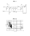
- FIG. 1 is a schematic view illustrating an input terminal of a driver IC according to an exemplary embodiment of the present disclosure.
- the circuit (100) for mitigating EMI generated from an input terminal includes a driver IC (140), an LC (Inductance-Capacitance) filter unit (110), a first capacitor (C1) connectively interposed between an outside power source (12V) for the driver IC (140) and a ground, a first diode (D1) serially connected to the outside power source (12V) and the LC filter unit (110), a plurality of second to fourth capacitors (C2, C3, C4) connectively interposed between a cathode terminal of the first diode (D1) and the ground, first and second resistors (120, 130) for absorbing EMI noise.
- EMI mitigating circuit includes a driver IC (140), an LC (Inductance-Capacitance) filter unit (110), a first capacitor (C1) connectively interposed between an outside power source (12V) for the driver IC (140) and a ground, a first diode (D1) serially connected to the outside power source (12V) and the
- the LC filter unit (110) may include an inductance (L1) connectively interposed between a power input port (a) of driver IC and a cathode terminal of the first diode (D1), and a fifth capacitor (C5) connectively interposed between the power input port (a) and a ground.
- L1 inductance
- D1 cathode terminal of the first diode
- C5 fifth capacitor
- a distal end of the first resistor (R1, 120) may be connected to the cathode terminal of the first diode (D1), and the other distal end of the first resistor (R1, 120) may be connected to an operation mode select input (SELECT). That is, the first resistor (R1, 120) is a pull-up resistor that pulls up the operation mode select input (SELECT) to a point (the cathode terminal of the first diode) where the power has passed the first diode (D1) to remove noise that is generated when the operation mode select input (SELECT) is opened.
- SELECT operation mode select input
- a distal end of a second resistor (R2, 130) may be connected to the operation mode select input (SELECT), and the other distal end of the second resistor (R2, 130) may be connected to an operation mode select port (b) of the driver IC.
- the first resistor (R1, 120) is an element for absorbing an EMI noise generated by the IC input terminal.
- a distal end of a sixth capacitor (C6) may be connected to the operation mode select input (SELECT), and the other distal end of the sixth capacitor (C6) may be connected to the ground.
- the plurality of capacitors (C1 to C4) serves to perform a decoupling operation, whereby low frequency or high frequency components inputted from an outside power (12V) are charged or discharged and noise included in the outside power (12V) is removed.
- the driver IC (140) may be AMIS30623.
- the circuit for mitigating EMI of driver IC of a vehicular head lamp is a circuit for removing EMI generated from an input terminal of IC including a power input port connected to a first input and an operation mode select port connected to a second input.
- the circuit may include a first diode connected to the first input, an LC filter unit connectively interposed a cathode terminal of the first diode and the power input port, and a first resistor connectively interposed between the cathode terminal of the first diode and the second input.
- the first input may be a power (e.g., DC 12V) for driving the IC
- the second input may be an operation mode select input, that is, a signal for the operation mode selection (e.g., for selecting a left head lamp or a right head lamp).
- a power for driving the IC is inputted into the first input and a signal for operation mode selection of the IC is inputted into the second input.
- the LC filter (110) may include an inductor (L1) connectively interposed between the cathode terminal of the first diode and the power input port (a), and a capacitor (C5) connectively interposed between the power input port (a) and a ground, where an inductance value of the inductor (L1) may be 2.2 ⁇ H, and a capacitance value of the capacitor (C5) may be 220 ⁇ F. Furthermore, the LC filter (110) may further include a second resistor connectively interposed between the second input and the operation mode select port (b), where each resistance value of the first resistor (120) and the second resistor (130) may be 1k ⁇ .
- the second input may be opened, where the operation mode select port (b) and the first input may be connected through the first resistor and the second resistor.
- the second input may be connected to the ground, where the operation mode select port (b) may be connected to the ground through the second resistor (130).
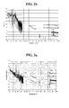
- FIG.2a is a schematic view illustrating an EMI generated by an input terminal of a driver IC according to prior art
- FIG.2b is a schematic view illustrating an EMI generated by an input terminal of a driver IC according to prior art.
- the EMI noise was measured in 10kHz ⁇ 108MHz, and the EMI noise in FIG.2a was measured from a discrete distance of 5cm, while the EMI noise in FIG. 2b was measured from a discrete distance of 75cm. It can be noted that measurements of both FIGS. 2a and 2b have passed 50dB ⁇ at low frequency band (10kHz ⁇ 50kHz), where 50dB ⁇ is a reference value which is a value specified in an exemplary application enabling to realize the driver IC for driving the head lamp of a vehicle. Therefore, the reference value may vary according to individual exemplary application.
- the above measured value has passed the reference value.
- the LC filter, the first resistor and the second resistor are added to the input terminal of the driver IC in the present disclosure.
- FIG.3a is a schematic view illustrating an EMI generated by an input terminal of a driver IC according to an exemplary embodiment of the present disclosure
- FIG.3b is a schematic view illustrating an EMI generated by an input terminal of a driver IC according to an exemplary embodiment of the present disclosure, where an EMI noise generated from the input terminal was measured respectively.
- the EMI noise was measured in 10kHz ⁇ 108MHz, and the EMI noise in FIG. 3a was measured from a discrete distance of 5cm, while the EMI noise in FIG. 3b was measured from a discrete distance of 75cm. It can be noted from FIGS. 3a and 3b that measurement result according to the exemplary embodiment of the present disclosure was below the reference value at low frequency band (10kHz ⁇ 50kHz), and the EMI noise has greatly reduced at an approximate range of 10kHz ⁇ 150kHz.
- the EMI mitigating circuit advantageously removes an EMI noise at low frequency band to prevent an erroneous operation of driver IC, whereby a driver and a passenger can be protected against a potential danger that may be generated by the erroneous operation.
Landscapes
- Engineering & Computer Science (AREA)
- Mathematical Physics (AREA)
- Physics & Mathematics (AREA)
- Computer Hardware Design (AREA)
- Computing Systems (AREA)
- General Engineering & Computer Science (AREA)
- Mechanical Engineering (AREA)
- Microelectronics & Electronic Packaging (AREA)
- Control Of Indicators Other Than Cathode Ray Tubes (AREA)
- Lighting Device Outwards From Vehicle And Optical Signal (AREA)
- Filters And Equalizers (AREA)
- Logic Circuits (AREA)
- Circuit Arrangement For Electric Light Sources In General (AREA)
Abstract
Description
- This application claims the benefit of earlier filing date and right of priority to Korean Patent Application No.
10-2011-0026297, filed on March 24, 2011 - Exemplary embodiments of the present disclosure may relate to a circuit for mitigating an EMI (Electro-Magnetic Interference) in input stage of a driver IC, and more particularly to an EMI mitigating circuit applied to an input terminal of a driver IC (Integrated Chip) driving an actuator in a head lamp of a vehicle.
- As used herein, the term EMI should be considered to refer generally to both electromagnetic interference and radio frequency interference (RFI) emissions, and the term "electromagnetic" should be considered to refer generally to electromagnetic and radio frequency.
- During normal operation, electronic equipment typically generates undesirable electromagnetic energy that can interfere with the operation of proximately located electronic equipment due to EMI transmission by radiation and conduction. The electromagnetic energy can exist over a wide range of wavelengths and frequencies. To minimize problems associated with EMI, sources of undesirable electromagnetic energy can be shielded and electrically grounded to reduce emissions into the surrounding environment. Alternatively, or additionally, susceptors of EMI can be similarly shielded and electrically grounded to protect them from EMI within the surrounding environment. Accordingly, shielding is designed to prevent both ingress and egress of electromagnetic energy relative to a barrier, a housing, or other enclosure in which the electronic equipment is disposed.
- EMI (Electro-Magnetic Interference) is regarded as a chronic noise problem as an operational frequency in electronic products increases. Particularly, the EMI problem has become more serious and a solution to address the EMI problem has become a pressing urgent necessity as the operational frequency in electronic products has expanded to several hundreds of MHz to several thousands of GHz.
- The EMI noise is a noise causing generation of mutual interference when electromagnetic wave generated by any one of an electrical circuitry, an element and/or a part is transmitted to another electrical circuitry, element and/or part.
- Unlike the conventional vehicles, the current vehicles are applied with electronic devices for convenience and safety, and manufactured with many electronic parts. Particularly, an adaptive head lamp system controlling movement of a head lamp of a vehicle is equipped with many electronic parts.
- The EMI is largely generated by electrical/electronic signals generated for controlling movement of the head lamp. As noted above, during normal operation, electronic equipment typically generates undesirable EMI that can interfere with operation of proximately located electronic equipment due to EMI transmission by radiation and conduction that can cause erroneous operation to the disadvantage and safety problem to a driver and passengers.
- Accordingly, it would be desirable and necessary to remove or mitigate the EMI in the electronic devices that causes potential danger.
- The present disclosure is disclosed to solve the abovementioned problems and disadvantages and the present disclosure is configured to solve the aforementioned disadvantages by providing a new circuit to an input terminal of an IC including a power input port of a driver IC including for driving a head lamp and an operational mode selection port.
- Technical subjects to be solved by the present disclosure are not restricted to the above-mentioned description, and any other technical problems not mentioned so far will be clearly appreciated from the following description by the skilled in the art. That is, the present disclosure will be understood more easily and other objects, characteristics, details and advantages thereof will become more apparent in the course of the following explanatory description, which is given, without intending to imply any limitation of the disclosure, with reference to the attached drawings.
- In one broad general aspect of the present disclosure, there is provided a circuit for mitigating EMI generated from an input terminal of an IC (Integrated Circuit) including a power input port connected to a first input and an operational mode selection port connected to a second input, the circuit comprising: a first diode connected to the first input; an LC filter unit connectively interposed a cathode terminal of the first diode and the power input port; and a first resistor connectively interposed between the cathode terminal of the first diode and the second input.
- Preferably, the first resistor is a pull-up resistor absorbing the EMI generated from the input terminal of the IC.
- Preferably, a power for driving the IC is inputted into the first input and a signal for operation mode selection of the IC is inputted into the second input
- Preferably, the LC filter unit includes an inductor connectively interposed between the cathode terminal of the first diode and the power input port, and a capacitor connectively interposed between the power input port and a ground, wherein an inductance value of the inductor is 2.2µH, and a capacitance value of the capacitor is 220 µF.
- Preferably, a resistance value of the first resistor is 1kQ.
- Preferably, the circuit further comprises a second resistor connectively interposed between the second input and the operation mode selection port.
- Preferably, the operation mode selection port and the first input are connected through the first and second resistors when the second input is opened.
- The circuit for mitigating EMI in input stage of a driver IC according to an exemplary embodiment of the present disclosure has an advantageous effect in that EMI noise at a low band of an input terminal of IC of head lamp can be removed to prevent erroneous operation and to secure stability.
- Accompanying drawings are included to provide a further understanding of arrangements and embodiments of the present disclosure and are incorporated in and constitute a part of this application. Now, non-limiting and non-exhaustive exemplary embodiments of the disclosure are described with reference to the following drawings, in which:
-
FIG. 1 is a schematic view illustrating an input terminal of a driver IC according to an exemplary embodiment of the present disclosure; -
FIG. 2a is a schematic view illustrating an EMI generated by an input terminal of a driver IC according to prior art; -
FIG. 2b is a schematic view illustrating an EMI generated by an input terminal of a driver IC according to prior art; -
FIG. 3a is a schematic view illustrating an EMI generated by an input terminal of a driver IC according to an exemplary embodiment of the present disclosure; and -
FIG. 3b is a schematic view illustrating an EMI generated by an input terminal of a driver IC according to an exemplary embodiment of the present disclosure. - Additional advantages, objects, and features of the disclosure will be set forth in part in the description which follows and in part will become apparent to those having ordinary skill in the art upon examination of the following or may be learned from practice of the disclosure. The objectives and other advantages of the disclosure may be realized and attained by the method particularly pointed out in the written description and claims hereof as well as the appended drawings.
- Hereinafter, exemplary embodiments of the present disclosure are described in detail with reference to the accompanying drawings. It will be appreciated that for simplicity and/or clarity of illustration, elements illustrated in the figure have not necessarily been drawn to scale. For example, the dimensions of some of the elements may be exaggerated relative to other elements for clarity. Further, if considered appropriate, reference numerals have been repeated among the figures to indicate corresponding and/or analogous elements.
- Particular terms may be defined to describe the disclosure in the best mode as known by the inventors. Accordingly, the meaning of specific terms or words used in the specification and the claims should not be limited to the literal or commonly employed sense, but should be construed in accordance with the spirit and scope of the disclosure. The definitions of these terms therefore may be determined based on the contents throughout the specification.
- In the following detailed description, numerous specific details are set forth to provide a thorough understanding of claimed subject matter. However, it will be understood by those skilled in the art that claimed subject matter may be practiced without these specific details. In other instances, well-known methods, procedures, components and/or circuits have not been described in detail.
- The term "and/or" may mean "and", it may mean "or", it may mean "exclusive-or", it may mean "one", it may mean "some, but not all", it may mean "neither", and/or it may mean "both", although the scope of claimed subject matter is not limited in this respect.
- In the following description and/or claims, the terms "comprise" and "include," along with their derivatives, may be used and are intended as synonyms for each other. Furthermore, the terms "including", "includes", "having", "has", "with", or variants thereof are used in the detailed description and/or the claims to denote non-exhaustive inclusion in a manner similar to the term "comprising".
- Words such as "thereafter," "then," "next," etc. are not intended to limit the order of the processes; these words are simply used to guide the reader through the description of the methods. The terms "first," "second," and the like, herein do not denote any order, quantity, or importance, but rather are used to distinguish one element from another, and the terms "a" and "an" herein do not denote a limitation of quantity, but rather denote the presence of at least one of the referenced item.
- In describing the present disclosure, detailed descriptions of constructions or processes known in the art may be omitted to avoid obscuring appreciation of the invention by a person of ordinary skill in the art with unnecessary detail regarding such known constructions and functions.
- Now, a circuit for mitigating EMI generated from an input terminal of an IC (Integrated Circuit) will be described in detail with reference to the accompanying drawings.
-
FIG. 1 is a schematic view illustrating an input terminal of a driver IC according to an exemplary embodiment of the present disclosure. - The circuit (100) for mitigating EMI generated from an input terminal (hereinafter referred to as EMI mitigating circuit) includes a driver IC (140), an LC (Inductance-Capacitance) filter unit (110), a first capacitor (C1) connectively interposed between an outside power source (12V) for the driver IC (140) and a ground, a first diode (D1) serially connected to the outside power source (12V) and the LC filter unit (110), a plurality of second to fourth capacitors (C2, C3, C4) connectively interposed between a cathode terminal of the first diode (D1) and the ground, first and second resistors (120, 130) for absorbing EMI noise.
- The LC filter unit (110) may include an inductance (L1) connectively interposed between a power input port (a) of driver IC and a cathode terminal of the first diode (D1), and a fifth capacitor (C5) connectively interposed between the power input port (a) and a ground.
- A distal end of the first resistor (R1, 120) may be connected to the cathode terminal of the first diode (D1), and the other distal end of the first resistor (R1, 120) may be connected to an operation mode select input (SELECT). That is, the first resistor (R1, 120) is a pull-up resistor that pulls up the operation mode select input (SELECT) to a point (the cathode terminal of the first diode) where the power has passed the first diode (D1) to remove noise that is generated when the operation mode select input (SELECT) is opened.
- Furthermore, a distal end of a second resistor (R2, 130) may be connected to the operation mode select input (SELECT), and the other distal end of the second resistor (R2, 130) may be connected to an operation mode select port (b) of the driver IC. The first resistor (R1, 120) is an element for absorbing an EMI noise generated by the IC input terminal.
- Furthermore, a distal end of a sixth capacitor (C6) may be connected to the operation mode select input (SELECT), and the other distal end of the sixth capacitor (C6) may be connected to the ground.
- The plurality of capacitors (C1 to C4) serves to perform a decoupling operation, whereby low frequency or high frequency components inputted from an outside power (12V) are charged or discharged and noise included in the outside power (12V) is removed. In a non-limiting example, the driver IC (140) may be AMIS30623.
- The circuit for mitigating EMI of driver IC of a vehicular head lamp according to the exemplary embodiment of the present disclosure is a circuit for removing EMI generated from an input terminal of IC including a power input port connected to a first input and an operation mode select port connected to a second input. Thus, the circuit may include a first diode connected to the first input, an LC filter unit connectively interposed a cathode terminal of the first diode and the power input port, and a first resistor connectively interposed between the cathode terminal of the first diode and the second input.
- The first input may be a power (e.g.,
DC 12V) for driving the IC, and the second input may be an operation mode select input, that is, a signal for the operation mode selection (e.g., for selecting a left head lamp or a right head lamp). In other words, a power for driving the IC is inputted into the first input and a signal for operation mode selection of the IC is inputted into the second input. - The LC filter (110) may include an inductor (L1) connectively interposed between the cathode terminal of the first diode and the power input port (a), and a capacitor (C5) connectively interposed between the power input port (a) and a ground, where an inductance value of the inductor (L1) may be 2.2µH, and a capacitance value of the capacitor (C5) may be 220 µF. Furthermore, the LC filter (110) may further include a second resistor connectively interposed between the second input and the operation mode select port (b), where each resistance value of the first resistor (120) and the second resistor (130) may be 1kΩ.
- In a non-limiting example, if the operation mode is a mode for controlling the left head lamp, the second input may be opened, where the operation mode select port (b) and the first input may be connected through the first resistor and the second resistor. In a non-limiting example, if the operation mode is a mode for controlling the right head lamp, the second input may be connected to the ground, where the operation mode select port (b) may be connected to the ground through the second resistor (130).
-
FIG.2a is a schematic view illustrating an EMI generated by an input terminal of a driver IC according to prior art, andFIG.2b is a schematic view illustrating an EMI generated by an input terminal of a driver IC according to prior art. - Referring to
FIGS. 2a and2b , the EMI noise was measured in 10kHz∼108MHz, and the EMI noise inFIG.2a was measured from a discrete distance of 5cm, while the EMI noise inFIG. 2b was measured from a discrete distance of 75cm. It can be noted that measurements of bothFIGS. 2a and2b have passed 50dBµ at low frequency band (10kHz∼50kHz), where 50dBµ is a reference value which is a value specified in an exemplary application enabling to realize the driver IC for driving the head lamp of a vehicle. Therefore, the reference value may vary according to individual exemplary application. - In case of realizing a circuit according to the prior art, the above measured value has passed the reference value. In order to satisfy the reference value, the LC filter, the first resistor and the second resistor are added to the input terminal of the driver IC in the present disclosure.
-
FIG.3a is a schematic view illustrating an EMI generated by an input terminal of a driver IC according to an exemplary embodiment of the present disclosure, andFIG.3b is a schematic view illustrating an EMI generated by an input terminal of a driver IC according to an exemplary embodiment of the present disclosure, where an EMI noise generated from the input terminal was measured respectively. - Referring to
FIGS. 3a and3b , the EMI noise was measured in 10kHz∼108MHz, and the EMI noise inFIG. 3a was measured from a discrete distance of 5cm, while the EMI noise inFIG. 3b was measured from a discrete distance of 75cm. It can be noted fromFIGS. 3a and3b that measurement result according to the exemplary embodiment of the present disclosure was below the reference value at low frequency band (10kHz∼50kHz), and the EMI noise has greatly reduced at an approximate range of 10kHz ∼150kHz. - As apparent from the foregoing, the EMI mitigating circuit according to the exemplary embodiment of the present disclosure advantageously removes an EMI noise at low frequency band to prevent an erroneous operation of driver IC, whereby a driver and a passenger can be protected against a potential danger that may be generated by the erroneous operation.
- While particular features or aspects may have been disclosed with respect to several embodiments, such features or aspects may be selectively combined with one or more other features and/or aspects of other embodiments as may be desired.
Claims (7)
- A circuit for mitigating EMI generated from an input terminal of an IC (Integrated Circuit) including a power input port connected to a first input and an operational mode selection port connected to a second input, the circuit characterized by: a first diode connected to the first input; an LC filter unit connectively interposed a cathode terminal of the first diode and the power input port; and a first resistor connectively interposed between the cathode terminal of the first diode and the second input.
- The circuit of claim 1, characterized in that the first resistor is a pull-up resistor absorbing the EMI generated from the input terminal of the IC.
- The circuit of claim 1, characterized in that a power for driving the IC is inputted into the first input and a signal for operation mode selection of the IC is inputted into the second input.
- The circuit of claim 1, characterized in that the LC filter unit includes an inductor connectively interposed between the cathode terminal of the first diode and the power input port, and a capacitor connectively interposed between the power input port and a ground, wherein an inductance value of the inductor is 2.2µH, and a capacitance value of the capacitor is 220 µF.
- The circuit of claim 1, characterized in that a resistance value of the first resistor is 1kΩ.
- The circuit of claim 1, characterized in that the circuit further comprises a second resistor connectively interposed between the second input and the operation mode selection port.
- The circuit of claim 6, characterized in that the operation mode selection port and the first input are connected through the first and second resistors when the second input is opened.
Applications Claiming Priority (1)
| Application Number | Priority Date | Filing Date | Title |
|---|---|---|---|
| KR1020110026297A KR101819233B1 (en) | 2011-03-24 | 2011-03-24 | A circuit for mitigating electromagnetic interference in input stage of a driver ic |
Publications (3)
| Publication Number | Publication Date |
|---|---|
| EP2503695A2 true EP2503695A2 (en) | 2012-09-26 |
| EP2503695A3 EP2503695A3 (en) | 2016-12-07 |
| EP2503695B1 EP2503695B1 (en) | 2019-12-18 |
Family
ID=46000714
Family Applications (1)
| Application Number | Title | Priority Date | Filing Date |
|---|---|---|---|
| EP12161092.7A Active EP2503695B1 (en) | 2011-03-24 | 2012-03-23 | A circuit for mitigating electromagnetic interference in input stage of a driver IC |
Country Status (5)
| Country | Link |
|---|---|
| US (1) | US8922299B2 (en) |
| EP (1) | EP2503695B1 (en) |
| JP (1) | JP6258571B2 (en) |
| KR (1) | KR101819233B1 (en) |
| CN (1) | CN102751862B (en) |
Families Citing this family (1)
| Publication number | Priority date | Publication date | Assignee | Title |
|---|---|---|---|---|
| CN104972966B (en) * | 2014-04-11 | 2025-09-05 | 万喻 | A method for solving EMC electromagnetic interference of motor vehicle and ship speakers and speaker |
Citations (1)
| Publication number | Priority date | Publication date | Assignee | Title |
|---|---|---|---|---|
| KR20110026297A (en) | 2009-09-07 | 2011-03-15 | 금오공과대학교 산학협력단 | Rebar connector for head rebar |
Family Cites Families (17)
| Publication number | Priority date | Publication date | Assignee | Title |
|---|---|---|---|---|
| JPH06113457A (en) * | 1992-09-30 | 1994-04-22 | Suzuki Motor Corp | Noise reduction circuit |
| US5650694A (en) * | 1995-03-31 | 1997-07-22 | Philips Electronics North America Corporation | Lamp controller with lamp status detection and safety circuitry |
| JPH11213517A (en) * | 1998-01-26 | 1999-08-06 | Mitsumi Electric Co Ltd | Integrated circuit for floppy disk drive |
| US6242990B1 (en) * | 1999-06-16 | 2001-06-05 | Tlc Precision Wafer Technology, Inc. | Quadrature phase shift keyed/bi-phase shift keyed modulator |
| JP2001160727A (en) * | 1999-12-01 | 2001-06-12 | Nec Niigata Ltd | Circuit board |
| US6313616B1 (en) * | 2000-09-21 | 2001-11-06 | Home Touch Lighting Systems Llc | Switching buck converter with floating regulator |
| CN2502485Y (en) | 2001-09-28 | 2002-07-24 | 北京硅谷浪潮科技发展有限公司 | High power factor electronic ballast for controlling high voltage gas discharge lamp |
| JP2003333861A (en) * | 2002-05-10 | 2003-11-21 | Canon Inc | Power supply device, design method thereof, and power generation device |
| JP2005224071A (en) * | 2004-02-09 | 2005-08-18 | Denso Corp | Battery control device |
| JP4499474B2 (en) | 2004-05-10 | 2010-07-07 | 株式会社小糸製作所 | Vehicle lighting |
| US7436127B2 (en) * | 2005-11-03 | 2008-10-14 | International Rectifier Corporation | Ballast control circuit |
| US20080211347A1 (en) * | 2007-03-02 | 2008-09-04 | Joshua Isaac Wright | Circuit System With Supply Voltage For Driving An Electromechanical Switch |
| DE102008029478B4 (en) * | 2008-06-20 | 2015-10-08 | Continental Automotive Gmbh | control module |
| EP2154771B1 (en) * | 2008-08-13 | 2011-10-26 | Osram AG | Circuit and method for reducing electromagnetic interference |
| JP5063572B2 (en) * | 2008-12-04 | 2012-10-31 | 三菱電機株式会社 | In-vehicle electronic control unit |
| CN201540530U (en) | 2009-11-06 | 2010-08-04 | 深圳市福瑞康电子有限公司 | Power adapter applicable to laptop |
| EP2499421B1 (en) * | 2009-11-09 | 2019-08-14 | Aktieboken 8626 Ab | High efficiency led lighting |
-
2011
- 2011-03-24 KR KR1020110026297A patent/KR101819233B1/en active Active
- 2011-09-23 US US13/241,883 patent/US8922299B2/en active Active
-
2012
- 2012-03-23 EP EP12161092.7A patent/EP2503695B1/en active Active
- 2012-03-26 JP JP2012069790A patent/JP6258571B2/en active Active
- 2012-03-26 CN CN201210082481.6A patent/CN102751862B/en active Active
Patent Citations (1)
| Publication number | Priority date | Publication date | Assignee | Title |
|---|---|---|---|---|
| KR20110026297A (en) | 2009-09-07 | 2011-03-15 | 금오공과대학교 산학협력단 | Rebar connector for head rebar |
Also Published As
| Publication number | Publication date |
|---|---|
| KR20120109030A (en) | 2012-10-08 |
| JP6258571B2 (en) | 2018-01-10 |
| US20120242424A1 (en) | 2012-09-27 |
| US8922299B2 (en) | 2014-12-30 |
| JP2012205311A (en) | 2012-10-22 |
| KR101819233B1 (en) | 2018-01-16 |
| CN102751862B (en) | 2015-02-18 |
| CN102751862A (en) | 2012-10-24 |
| EP2503695A3 (en) | 2016-12-07 |
| EP2503695B1 (en) | 2019-12-18 |
Similar Documents
| Publication | Publication Date | Title |
|---|---|---|
| EP2891576B1 (en) | Low voltage electromagnetic interference filter of electric vehicle | |
| US10063209B2 (en) | Noise filter | |
| US8698571B2 (en) | Circuit for improving the immunity performance of a vehicle network | |
| CN111656660A (en) | EMI suppression for vehicles | |
| CN103166592B (en) | Integrated passive device with electrostatic protection mechanism | |
| US9825522B2 (en) | Method and apparatus for coupling cancellation | |
| JP2013110580A (en) | Noise filter and electronic apparatus equipped with the same | |
| EP2503695B1 (en) | A circuit for mitigating electromagnetic interference in input stage of a driver IC | |
| Rostamzadeh et al. | Automotive AM-band radiated emission mitigation techniques, a practical approach | |
| US20200185864A1 (en) | Module For A High-Current Plug And/Or A High-Current Cable, High-Current Plug, And Method Of Influencing The EMC Behaviour | |
| DE102005037579A1 (en) | Electronic control unit | |
| US12224886B2 (en) | Electronic control device | |
| US7145783B2 (en) | Apparatus reducing radiated emission from electronic modules | |
| US8786071B2 (en) | Wiring pattern having a stub wire | |
| US12069813B2 (en) | Electronic device and electric power steering apparatus having electronic device mounted thereto | |
| JP7588031B2 (en) | Electronic Control Unit | |
| CN210258300U (en) | Input protection circuit of electronic equipment of vehicle and vehicle | |
| KR101290405B1 (en) | Earth leakage breaker | |
| US20090058559A1 (en) | Microprocessor common-mode emissions reduction circuit | |
| US20060221584A1 (en) | Method for ground noise suppression | |
| US20250219606A1 (en) | Signal transmission circuit and electronic device | |
| Wang | Electromagnetic Compatibility Design for Mobile Target Positioning Terminals | |
| Emilio | AUTOMOTIVE EMC | |
| KR101789830B1 (en) | A circuit of input and output stage of a driver ic configured to mitigate electromagnetic interference | |
| US20020047728A1 (en) | Integrated circuit |
Legal Events
| Date | Code | Title | Description |
|---|---|---|---|
| PUAI | Public reference made under article 153(3) epc to a published international application that has entered the european phase |
Free format text: ORIGINAL CODE: 0009012 |
|
| AK | Designated contracting states |
Kind code of ref document: A2 Designated state(s): AL AT BE BG CH CY CZ DE DK EE ES FI FR GB GR HR HU IE IS IT LI LT LU LV MC MK MT NL NO PL PT RO RS SE SI SK SM TR |
|
| AX | Request for extension of the european patent |
Extension state: BA ME |
|
| PUAL | Search report despatched |
Free format text: ORIGINAL CODE: 0009013 |
|
| AK | Designated contracting states |
Kind code of ref document: A3 Designated state(s): AL AT BE BG CH CY CZ DE DK EE ES FI FR GB GR HR HU IE IS IT LI LT LU LV MC MK MT NL NO PL PT RO RS SE SI SK SM TR |
|
| AX | Request for extension of the european patent |
Extension state: BA ME |
|
| RIC1 | Information provided on ipc code assigned before grant |
Ipc: H03K 19/003 20060101AFI20161102BHEP |
|
| STAA | Information on the status of an ep patent application or granted ep patent |
Free format text: STATUS: REQUEST FOR EXAMINATION WAS MADE |
|
| RAP1 | Party data changed (applicant data changed or rights of an application transferred) |
Owner name: LG INNOTEK CO., LTD. |
|
| 17P | Request for examination filed |
Effective date: 20170424 |
|
| RBV | Designated contracting states (corrected) |
Designated state(s): AL AT BE BG CH CY CZ DE DK EE ES FI FR GB GR HR HU IE IS IT LI LT LU LV MC MK MT NL NO PL PT RO RS SE SI SK SM TR |
|
| GRAP | Despatch of communication of intention to grant a patent |
Free format text: ORIGINAL CODE: EPIDOSNIGR1 |
|
| STAA | Information on the status of an ep patent application or granted ep patent |
Free format text: STATUS: GRANT OF PATENT IS INTENDED |
|
| INTG | Intention to grant announced |
Effective date: 20190709 |
|
| GRAS | Grant fee paid |
Free format text: ORIGINAL CODE: EPIDOSNIGR3 |
|
| GRAA | (expected) grant |
Free format text: ORIGINAL CODE: 0009210 |
|
| STAA | Information on the status of an ep patent application or granted ep patent |
Free format text: STATUS: THE PATENT HAS BEEN GRANTED |
|
| AK | Designated contracting states |
Kind code of ref document: B1 Designated state(s): AL AT BE BG CH CY CZ DE DK EE ES FI FR GB GR HR HU IE IS IT LI LT LU LV MC MK MT NL NO PL PT RO RS SE SI SK SM TR |
|
| REG | Reference to a national code |
Ref country code: GB Ref legal event code: FG4D |
|
| REG | Reference to a national code |
Ref country code: CH Ref legal event code: EP |
|
| REG | Reference to a national code |
Ref country code: DE Ref legal event code: R096 Ref document number: 602012066503 Country of ref document: DE |
|
| REG | Reference to a national code |
Ref country code: IE Ref legal event code: FG4D |
|
| REG | Reference to a national code |
Ref country code: AT Ref legal event code: REF Ref document number: 1215691 Country of ref document: AT Kind code of ref document: T Effective date: 20200115 |
|
| REG | Reference to a national code |
Ref country code: NL Ref legal event code: MP Effective date: 20191218 |
|
| PG25 | Lapsed in a contracting state [announced via postgrant information from national office to epo] |
Ref country code: GR Free format text: LAPSE BECAUSE OF FAILURE TO SUBMIT A TRANSLATION OF THE DESCRIPTION OR TO PAY THE FEE WITHIN THE PRESCRIBED TIME-LIMIT Effective date: 20200319 Ref country code: NO Free format text: LAPSE BECAUSE OF FAILURE TO SUBMIT A TRANSLATION OF THE DESCRIPTION OR TO PAY THE FEE WITHIN THE PRESCRIBED TIME-LIMIT Effective date: 20200318 Ref country code: LT Free format text: LAPSE BECAUSE OF FAILURE TO SUBMIT A TRANSLATION OF THE DESCRIPTION OR TO PAY THE FEE WITHIN THE PRESCRIBED TIME-LIMIT Effective date: 20191218 Ref country code: LV Free format text: LAPSE BECAUSE OF FAILURE TO SUBMIT A TRANSLATION OF THE DESCRIPTION OR TO PAY THE FEE WITHIN THE PRESCRIBED TIME-LIMIT Effective date: 20191218 Ref country code: SE Free format text: LAPSE BECAUSE OF FAILURE TO SUBMIT A TRANSLATION OF THE DESCRIPTION OR TO PAY THE FEE WITHIN THE PRESCRIBED TIME-LIMIT Effective date: 20191218 Ref country code: FI Free format text: LAPSE BECAUSE OF FAILURE TO SUBMIT A TRANSLATION OF THE DESCRIPTION OR TO PAY THE FEE WITHIN THE PRESCRIBED TIME-LIMIT Effective date: 20191218 Ref country code: BG Free format text: LAPSE BECAUSE OF FAILURE TO SUBMIT A TRANSLATION OF THE DESCRIPTION OR TO PAY THE FEE WITHIN THE PRESCRIBED TIME-LIMIT Effective date: 20200318 |
|
| REG | Reference to a national code |
Ref country code: LT Ref legal event code: MG4D |
|
| PG25 | Lapsed in a contracting state [announced via postgrant information from national office to epo] |
Ref country code: RS Free format text: LAPSE BECAUSE OF FAILURE TO SUBMIT A TRANSLATION OF THE DESCRIPTION OR TO PAY THE FEE WITHIN THE PRESCRIBED TIME-LIMIT Effective date: 20191218 Ref country code: HR Free format text: LAPSE BECAUSE OF FAILURE TO SUBMIT A TRANSLATION OF THE DESCRIPTION OR TO PAY THE FEE WITHIN THE PRESCRIBED TIME-LIMIT Effective date: 20191218 |
|
| PG25 | Lapsed in a contracting state [announced via postgrant information from national office to epo] |
Ref country code: AL Free format text: LAPSE BECAUSE OF FAILURE TO SUBMIT A TRANSLATION OF THE DESCRIPTION OR TO PAY THE FEE WITHIN THE PRESCRIBED TIME-LIMIT Effective date: 20191218 |
|
| PG25 | Lapsed in a contracting state [announced via postgrant information from national office to epo] |
Ref country code: NL Free format text: LAPSE BECAUSE OF FAILURE TO SUBMIT A TRANSLATION OF THE DESCRIPTION OR TO PAY THE FEE WITHIN THE PRESCRIBED TIME-LIMIT Effective date: 20191218 Ref country code: PT Free format text: LAPSE BECAUSE OF FAILURE TO SUBMIT A TRANSLATION OF THE DESCRIPTION OR TO PAY THE FEE WITHIN THE PRESCRIBED TIME-LIMIT Effective date: 20200513 Ref country code: CZ Free format text: LAPSE BECAUSE OF FAILURE TO SUBMIT A TRANSLATION OF THE DESCRIPTION OR TO PAY THE FEE WITHIN THE PRESCRIBED TIME-LIMIT Effective date: 20191218 Ref country code: EE Free format text: LAPSE BECAUSE OF FAILURE TO SUBMIT A TRANSLATION OF THE DESCRIPTION OR TO PAY THE FEE WITHIN THE PRESCRIBED TIME-LIMIT Effective date: 20191218 Ref country code: RO Free format text: LAPSE BECAUSE OF FAILURE TO SUBMIT A TRANSLATION OF THE DESCRIPTION OR TO PAY THE FEE WITHIN THE PRESCRIBED TIME-LIMIT Effective date: 20191218 |
|
| PG25 | Lapsed in a contracting state [announced via postgrant information from national office to epo] |
Ref country code: IS Free format text: LAPSE BECAUSE OF FAILURE TO SUBMIT A TRANSLATION OF THE DESCRIPTION OR TO PAY THE FEE WITHIN THE PRESCRIBED TIME-LIMIT Effective date: 20200418 Ref country code: SK Free format text: LAPSE BECAUSE OF FAILURE TO SUBMIT A TRANSLATION OF THE DESCRIPTION OR TO PAY THE FEE WITHIN THE PRESCRIBED TIME-LIMIT Effective date: 20191218 Ref country code: SM Free format text: LAPSE BECAUSE OF FAILURE TO SUBMIT A TRANSLATION OF THE DESCRIPTION OR TO PAY THE FEE WITHIN THE PRESCRIBED TIME-LIMIT Effective date: 20191218 |
|
| REG | Reference to a national code |
Ref country code: DE Ref legal event code: R097 Ref document number: 602012066503 Country of ref document: DE |
|
| REG | Reference to a national code |
Ref country code: AT Ref legal event code: MK05 Ref document number: 1215691 Country of ref document: AT Kind code of ref document: T Effective date: 20191218 |
|
| PLBE | No opposition filed within time limit |
Free format text: ORIGINAL CODE: 0009261 |
|
| STAA | Information on the status of an ep patent application or granted ep patent |
Free format text: STATUS: NO OPPOSITION FILED WITHIN TIME LIMIT |
|
| PG25 | Lapsed in a contracting state [announced via postgrant information from national office to epo] |
Ref country code: ES Free format text: LAPSE BECAUSE OF FAILURE TO SUBMIT A TRANSLATION OF THE DESCRIPTION OR TO PAY THE FEE WITHIN THE PRESCRIBED TIME-LIMIT Effective date: 20191218 Ref country code: MC Free format text: LAPSE BECAUSE OF FAILURE TO SUBMIT A TRANSLATION OF THE DESCRIPTION OR TO PAY THE FEE WITHIN THE PRESCRIBED TIME-LIMIT Effective date: 20191218 Ref country code: DK Free format text: LAPSE BECAUSE OF FAILURE TO SUBMIT A TRANSLATION OF THE DESCRIPTION OR TO PAY THE FEE WITHIN THE PRESCRIBED TIME-LIMIT Effective date: 20191218 |
|
| REG | Reference to a national code |
Ref country code: CH Ref legal event code: PL |
|
| 26N | No opposition filed |
Effective date: 20200921 |
|
| PG25 | Lapsed in a contracting state [announced via postgrant information from national office to epo] |
Ref country code: AT Free format text: LAPSE BECAUSE OF FAILURE TO SUBMIT A TRANSLATION OF THE DESCRIPTION OR TO PAY THE FEE WITHIN THE PRESCRIBED TIME-LIMIT Effective date: 20191218 Ref country code: SI Free format text: LAPSE BECAUSE OF FAILURE TO SUBMIT A TRANSLATION OF THE DESCRIPTION OR TO PAY THE FEE WITHIN THE PRESCRIBED TIME-LIMIT Effective date: 20191218 |
|
| REG | Reference to a national code |
Ref country code: BE Ref legal event code: MM Effective date: 20200331 |
|
| PG25 | Lapsed in a contracting state [announced via postgrant information from national office to epo] |
Ref country code: LU Free format text: LAPSE BECAUSE OF NON-PAYMENT OF DUE FEES Effective date: 20200323 |
|
| PG25 | Lapsed in a contracting state [announced via postgrant information from national office to epo] |
Ref country code: IE Free format text: LAPSE BECAUSE OF NON-PAYMENT OF DUE FEES Effective date: 20200323 Ref country code: LI Free format text: LAPSE BECAUSE OF NON-PAYMENT OF DUE FEES Effective date: 20200331 Ref country code: CH Free format text: LAPSE BECAUSE OF NON-PAYMENT OF DUE FEES Effective date: 20200331 Ref country code: IT Free format text: LAPSE BECAUSE OF FAILURE TO SUBMIT A TRANSLATION OF THE DESCRIPTION OR TO PAY THE FEE WITHIN THE PRESCRIBED TIME-LIMIT Effective date: 20191218 |
|
| PG25 | Lapsed in a contracting state [announced via postgrant information from national office to epo] |
Ref country code: BE Free format text: LAPSE BECAUSE OF NON-PAYMENT OF DUE FEES Effective date: 20200331 Ref country code: PL Free format text: LAPSE BECAUSE OF FAILURE TO SUBMIT A TRANSLATION OF THE DESCRIPTION OR TO PAY THE FEE WITHIN THE PRESCRIBED TIME-LIMIT Effective date: 20191218 |
|
| GBPC | Gb: european patent ceased through non-payment of renewal fee |
Effective date: 20200323 |
|
| PG25 | Lapsed in a contracting state [announced via postgrant information from national office to epo] |
Ref country code: GB Free format text: LAPSE BECAUSE OF NON-PAYMENT OF DUE FEES Effective date: 20200323 |
|
| PG25 | Lapsed in a contracting state [announced via postgrant information from national office to epo] |
Ref country code: TR Free format text: LAPSE BECAUSE OF FAILURE TO SUBMIT A TRANSLATION OF THE DESCRIPTION OR TO PAY THE FEE WITHIN THE PRESCRIBED TIME-LIMIT Effective date: 20191218 Ref country code: MT Free format text: LAPSE BECAUSE OF FAILURE TO SUBMIT A TRANSLATION OF THE DESCRIPTION OR TO PAY THE FEE WITHIN THE PRESCRIBED TIME-LIMIT Effective date: 20191218 Ref country code: CY Free format text: LAPSE BECAUSE OF FAILURE TO SUBMIT A TRANSLATION OF THE DESCRIPTION OR TO PAY THE FEE WITHIN THE PRESCRIBED TIME-LIMIT Effective date: 20191218 |
|
| PG25 | Lapsed in a contracting state [announced via postgrant information from national office to epo] |
Ref country code: MK Free format text: LAPSE BECAUSE OF FAILURE TO SUBMIT A TRANSLATION OF THE DESCRIPTION OR TO PAY THE FEE WITHIN THE PRESCRIBED TIME-LIMIT Effective date: 20191218 |
|
| PGFP | Annual fee paid to national office [announced via postgrant information from national office to epo] |
Ref country code: DE Payment date: 20260220 Year of fee payment: 15 |
|
| PGFP | Annual fee paid to national office [announced via postgrant information from national office to epo] |
Ref country code: FR Payment date: 20260224 Year of fee payment: 15 |