EP2503589A2 - Multi-stage formation of thin-films for photovoltaic devices - Google Patents
Multi-stage formation of thin-films for photovoltaic devices Download PDFInfo
- Publication number
- EP2503589A2 EP2503589A2 EP12002005A EP12002005A EP2503589A2 EP 2503589 A2 EP2503589 A2 EP 2503589A2 EP 12002005 A EP12002005 A EP 12002005A EP 12002005 A EP12002005 A EP 12002005A EP 2503589 A2 EP2503589 A2 EP 2503589A2
- Authority
- EP
- European Patent Office
- Prior art keywords
- chemical
- film
- chemical composition
- substrate
- range
- Prior art date
- Legal status (The legal status is an assumption and is not a legal conclusion. Google has not performed a legal analysis and makes no representation as to the accuracy of the status listed.)
- Granted
Links
Images


Classifications
-
- H—ELECTRICITY
- H10—SEMICONDUCTOR DEVICES; ELECTRIC SOLID-STATE DEVICES NOT OTHERWISE PROVIDED FOR
- H10P—GENERIC PROCESSES OR APPARATUS FOR THE MANUFACTURE OR TREATMENT OF DEVICES COVERED BY CLASS H10
- H10P14/00—Formation of materials, e.g. in the shape of layers or pillars
- H10P14/20—Formation of materials, e.g. in the shape of layers or pillars of semiconductor materials
- H10P14/34—Deposited materials, e.g. layers
- H10P14/3402—Deposited materials, e.g. layers characterised by the chemical composition
- H10P14/3436—Deposited materials, e.g. layers characterised by the chemical composition being chalcogenide semiconductor materials not being oxides, e.g. ternary compounds
-
- H—ELECTRICITY
- H10—SEMICONDUCTOR DEVICES; ELECTRIC SOLID-STATE DEVICES NOT OTHERWISE PROVIDED FOR
- H10F—INORGANIC SEMICONDUCTOR DEVICES SENSITIVE TO INFRARED RADIATION, LIGHT, ELECTROMAGNETIC RADIATION OF SHORTER WAVELENGTH OR CORPUSCULAR RADIATION
- H10F77/00—Constructional details of devices covered by this subclass
- H10F77/10—Semiconductor bodies
- H10F77/12—Active materials
- H10F77/126—Active materials comprising only Group I-III-VI chalcopyrite materials, e.g. CuInSe2, CuGaSe2 or CuInGaSe2 [CIGS]
-
- H—ELECTRICITY
- H10—SEMICONDUCTOR DEVICES; ELECTRIC SOLID-STATE DEVICES NOT OTHERWISE PROVIDED FOR
- H10P—GENERIC PROCESSES OR APPARATUS FOR THE MANUFACTURE OR TREATMENT OF DEVICES COVERED BY CLASS H10
- H10P14/00—Formation of materials, e.g. in the shape of layers or pillars
- H10P14/20—Formation of materials, e.g. in the shape of layers or pillars of semiconductor materials
- H10P14/203—Formation of materials, e.g. in the shape of layers or pillars of semiconductor materials using transformation of metal, e.g. oxidation or nitridation
-
- H—ELECTRICITY
- H10—SEMICONDUCTOR DEVICES; ELECTRIC SOLID-STATE DEVICES NOT OTHERWISE PROVIDED FOR
- H10P—GENERIC PROCESSES OR APPARATUS FOR THE MANUFACTURE OR TREATMENT OF DEVICES COVERED BY CLASS H10
- H10P14/00—Formation of materials, e.g. in the shape of layers or pillars
- H10P14/20—Formation of materials, e.g. in the shape of layers or pillars of semiconductor materials
- H10P14/34—Deposited materials, e.g. layers
- H10P14/3402—Deposited materials, e.g. layers characterised by the chemical composition
- H10P14/3424—Deposited materials, e.g. layers characterised by the chemical composition being Group IIB-VIA materials
- H10P14/3432—Tellurides
-
- Y—GENERAL TAGGING OF NEW TECHNOLOGICAL DEVELOPMENTS; GENERAL TAGGING OF CROSS-SECTIONAL TECHNOLOGIES SPANNING OVER SEVERAL SECTIONS OF THE IPC; TECHNICAL SUBJECTS COVERED BY FORMER USPC CROSS-REFERENCE ART COLLECTIONS [XRACs] AND DIGESTS
- Y02—TECHNOLOGIES OR APPLICATIONS FOR MITIGATION OR ADAPTATION AGAINST CLIMATE CHANGE
- Y02E—REDUCTION OF GREENHOUSE GAS [GHG] EMISSIONS, RELATED TO ENERGY GENERATION, TRANSMISSION OR DISTRIBUTION
- Y02E10/00—Energy generation through renewable energy sources
- Y02E10/50—Photovoltaic [PV] energy
- Y02E10/541—CuInSe2 material PV cells
Definitions
- the present invention relates to a method for forming a compound material thin film, such as a semiconductor thin-film suitable for use in photovoltaic solar cells and other devices.
- PV-based renewable-energy sources generate energy, in the form of electricity, by harnessing electromagnetic radiation, such as sunlight.
- PV applications are not limited to any particular area of the world and/or any given sector of the economy.
- an off-grid installation of the PV source provides the only available source of electricity.
- the PV source may, for example, source electricity to an electrical grid to supplement and/or reduce the amount of conventional energy distributed from the electrical grid.
- a PV source is in general any electric system containing a PV device, such as a PV cell or a PV module.
- PV devices are frequently used to convert optical energy into electrical energy.
- a photovoltaic device is made of one or two semiconductors with p-doped and n-doped regions.
- the commercialization of PV devices depends on technological advances that lead to higher efficiencies and lower cost of such devices.
- the cost of electricity can be significantly reduced by using PV devices constructed from compound thin film semiconductors, such as copper indium gallium selenide (CIGS).
- CGS copper indium gallium selenide
- CdTe films may be manufactured in a number of different ways, which include electro-deposition and vapor transport deposition.
- the CVD process is relatively expensive and not suitable for compound semiconductors, such as CIGS.
- Less expensive techniques developed for CdTe are also not applicable for other thin-film PV materials.
- CIGS films are mainly made using either an elemental co-evaporation process or a two-stage process, in which sputtering of a precursor film is followed by its selenization.
- the two-stage process is relatively easier to scale up in volume in comparison with the co-evaporation process, but it has drawbacks, such as loss of adhesion between the absorber layer and the back contact layer during selenization.
- a method for producing a film of compound material.
- the method includes providing a substrate and depositing a film on the substrate.
- the deposited film has a first chemical composition that includes at least one first chemical element and at least one second chemical element.
- At least one residual chemical reaction is induced in the deposited film using a source containing at least one second chemical element to thereby increase the content of at least one second chemical element in the deposited film so that the deposited film has a second chemical composition.
- the content of at least one second element in the second chemical composition is larger than the content of at least one second element in the first chemical composition.
- a method for producing a thin-film solar cell that includes depositing a first contact layer on a substrate and producing an absorber layer over the first contact layer.
- a window layer and a second contact layer are deposited over the absorber layer.
- the absorber layer is produced by a process that includes depositing a film over the first contact layer.
- the deposited film has a first chemical composition that includes at least one first chemical element and a second chemical element.
- a residual chemical reaction is induced in the deposited film using a source containing the second chemical element to thereby increase the content of the second chemical element in the deposited film so that the deposited film has a second chemical composition.
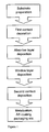
- FIG.1 shows a process for producing a thin-film solar cell.
- FIG.2 shows a substrate configuration of a thin-film solar cell
- FIG.3 shows a superstrate configuration of a thin-film solar cell
- FIG.4 shows a multi-stage formation of a binary compound thin-film.
- FIG.5 shows a multi-stage formation of a ternary compound thin-film.
- FIG.6 shows a multi-stage formation of a CIGS compound thin-film.
- FIG.7 shows a process for depositing a CIGS* film.
- FIG.8 shows a selenization process of a CIGS* film.
- FIG.1 illustrates an example of a process for manufacturing the thin-film photovoltaic (PV) device 200 shown in FIG.2 .
- This process includes several steps starting with the substrate preparation.
- Substrate 210 may be a glass sheet, a metal foil or a plastic film.
- First contact layer 220 may be deposited onto substrate 210 using a sputtering process.
- the first contact may serve as the back contact and contain metals, such as molybdenum (Mo), or transparent conducting oxides (TCO), such as tin oxide (SnO 2 ).
- the next optional processing step may include a laser scribing process, in which the first contact layer is divided into several electrically disconnected regions that in turn define individual PV cells.
- a thin absorber layer 230 is deposited on top of the first contact layer 220 using a multi-stage deposition process, which will be described in detail below.
- the absorber material may be based on CIGS, CdTe, a-Si, organic semiconductors and other thin-film semiconductors.
- a thin layer of another semiconductor material may be then deposited by a sputtering process, for instance, to produce a window layer 240, thus forming a pn junction with the absorber layer 230 underneath.
- Additional optional processing may include a mechanical scribing process, in which the absorber and window layers are divided into several electrically disconnected regions that in turn define individual PV cells.
- a second contact layer 250 is produced to create a functioning PV device 200.
- the second contact may serve as the front contact and contain TCO, such as indium tin oxide (ITO) or Al-doped zinc oxide (AZO).
- TCO such as indium tin oxide (ITO) or Al-doped zinc oxide (AZO).
- this manufacturing process may include various subsequent steps such as additional mechanical scribing, deposition of metal grid contacts, anti-reflection coating, lamination, packaging, etc.
- the manufacturing process of FIG.1 may be modified to produce the thin-film PV device 300 illustrated in FIG.3 .
- the window layer deposition precedes the absorber layer deposition.
- PV device 300 includes substrate 310, first contact layer 320, window layer 330, absorber layer 340, and second contact 350.
- the first contact may serve as the front contact and the second contact may serve as the back contact.
- absorber layers 230 and 340 may be formed using a multi-stage process, an example of which is shown in FIG.4 .
- a film is produced with a chemical composition AB 1-z , which may be similar or close to the chemical composition of a compound PV semiconductor AB, where A and B are different chemical elements and A may also be an alloy of different chemical elements.
- the value of (1-z) where z is the chemical deficiency of element B, can be defined as the ratio between the initial element B content to the final element B content; z may be in the range of 0.05 to 0.95, preferably in the range of 0.15-0.4.
- the compound semiconductor AB it is generally preferable for the compound semiconductor AB to be sufficiently stoichiometric and thus have a single phase crystalline structure at room temperature.
- the compound material AB 1-z may be non-stoichiometric and thus contain different crystalline phases. In the latter case the composition AB 1-z refers to the composition averaged across the volume of the deposited thin film.
- Compound material AB 1-z may also differ from the compound semiconductor AB in its physical properties, e.g. it may be an electrical conductor rather than a semiconductor.
- Compound material AB 1-z in the film may be a mixture of its constituent elements, e.g. a mixture of fine powders of elements A and B, respectively, wherein the characteristic particle size may be less than one micron, preferably in the range of 5-50 nm. It is preferable however that the compound material AB 1-z is a fully reacted, chemically stable material that is not just a mixture of its constituent elements. In this material chemical bonds are formed between its different elements and its chemical composition and crystalline structure may be substantially homogeneous from large to very small scales ( ⁇ few nm).
- a thin film comprising semiconductor AB 1-z may be deposited using a variety of approaches, including a physical vapor deposition (PVD) process, a magnetron sputtering process, an elemental co-evaporation, a non-vacuum nanoparticle deposition and others.
- PVD physical vapor deposition
- a pre-reacted bulk material having chemical composition AB 1-z may be dispersed and deposited onto a substrate in the form of a thin film with substantially the same chemical composition AB 1-z .
- a residual chemical reaction process is induced in the film when it is placed in an atmosphere of vapor containing element B.
- a PV absorber film is produced with the chemical composition AB.
- Chemical elements A and B may be, for example, chemical elements selected from groups II and VI, respectively.
- Group II elements include such elements as Mg, Zn, Cd, and Hg, whereas group VI elements include S, Se and Te.
- the latter group of elements is commonly known as chalcogens and the compound materials based on these elements are called chalcogenides.
- the compound chalcogen semiconductor AB may be CdTe.
- This aforementioned process is also applicable to compound semiconductor materials comprising more than two constituent chemical elements.
- a film having chemical composition ABC 1-z is first deposited onto a substrate. Afterwards, a residual chemical reaction is used to change the chemical composition of the film to ABC.
- Chemical elements A, B and C may be, for example, chemical elements from groups I, III and VI, respectively.
- Group I elements include such elements as Cu, Ag and Au
- group III elements include Al, In, Ga and Tl
- group VI elements include S, Se and Te.
- the compound semiconductor ABC may be, for example, CuInSe 2 .
- chemical elements from other groups may be used, e.g. Sn from group IV.
- the multi-stage process described above may be used with quaternary semiconductors and other materials comprising more than four elements.
- chemical elements from either group I, group III or group VI may be partially substituted with different elements from the same group.
- Cu may be partially substituted with Ag
- In may be partially substituted with Ga
- Se may be partially substituted with S.
- substitution does not alter the basic crystalline structure of the material and therefore does not produce any associated crystalline defects. It is frequently used to change electronic and optical properties of the material, e.g. to increase the optical bandgap in CuInSe 2 one may substitute In fully or partially with Ga.
- the multi-stage formation process is particularly applicable to compound semiconductor materials comprising more than two constituent chemical elements.
- the multi-stage process may include multiple residual reaction steps each corresponding to a specific deficient element.
- a film having an initial chemical composition AB 1-y C 1-z is first deposited onto a substrate, where elements B and C are deficient.
- several residual chemical reaction steps are used to change the chemical composition of the deposited film to ABC as shown in FIG.5 .
- an additional quantity y of element B is provided to produce a film with an intermediate composition ABC 1-z .
- an additional quantity z of element C is provided to produce a film with the final composition ABC. It also may be possible to combine multiple residual reactions in a single processing step, where more than a single element is added to the chemical composition (e.g. B and C in the above example).
- FIG.6 shows an example of a multi-stage formation process that employs a CIGS film.
- a thin CIGS * film is produced with a chemical composition Cu x In 1-y Ga y Se 2(1-z) , which is close to the chemical composition of a compound PV semiconductor Cu x In 1-y Ga y Se 2 .
- the Cu content x may be in the range of 0.6 to 1.0, and preferably in the range of 0.8-0.95.
- the Ga content y which determines the CIGS optical bandgap, may be in the range of 0.1-1.0, and preferably in the range of 0.2-0.35.
- the Se deficiency z may be in the range of 0.1-0.9, and preferably in the range of 0.5- 0.85.
- a residual selenization process is used to induce additional chemical reactions in the deposited film to thereby adjust the chemical composition of the film so that it has the composition Cu x In 1-y Ga y Se 2 .
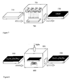
- FIG.7 shows schematically a method for the deposition of CIGS* thin films.
- the CIGS * film may be deposited by evaporation and/or sputtering from one or more targets (721, 722, 723 and 724).
- Target materials may include high purity single elements, such as Cu, In, Ga, Se and S, partially reacted compounds and allows, such as Cu 2 Se, InGa, In x Se, Ga y Se, CuInGa and others, and fully reacted compounds, such as Cu x In 1-y Ga y Se 2(1-z) .
- a flat rigid substrate 710 may be used that has been prepared and processed prior to the deposition as described above.
- a vacuum deposition system 720 may employ, for example, a magnetron sputtering tool to deposit a thin CIGS* film 730 on the substrate.
- DC magnetron sputtering may be used for electrically conductive targets such as metallic alloys, which is a faster process compared to the RF sputtering that is normally used with dielectrics.
- non-vacuum deposition methods such as ink jet printing may be used.
- the CIGS* bulk material may be pulverized into small particles, dispersed, coated on the substrate and then annealed to form a thin CIGS* film.
- FIG.8 shows schematically a method for the residual selenization step, in which a thin CIGS* film on a substrate 810 having the initial composition Cu x In 1-y Ga y Se 2(1-z) is first transported into a chamber 820.
- Se-containing gas such as H 2 Se or Se 2
- the film on the substrate 810 is heated.
- Se atoms diffuse into the film to complete the formation of the CIGS film 830, which has the final composition Cu x In 1-y Ga y Se 2 .
- the chemical reaction may be controlled by temperature and time.
- residual selenization may be accomplished using temperatures in the range from 400°C to 550°C and a reaction time in a range of 5 to 30 minutes.
- the reaction time may be chosen to allow a sufficient amount of Se (in proportion to Se deficiency) to diffuse and react with the rest of the elements in the film.
- Selenization and other similar reactions, such as for example sulfurization, under appropriate conditions of temperature and pressure may be self-limiting. This implies that upon the formation of a stoichiometric compound of Cu x In 1-y Ga y Se 2 , further incorporation of Se into the film stops and the selenization reaction terminates.
- An example of appropriate conditions for such a self-limiting reaction may be a sufficiently high processing temperature, at which chalcogens, which are in excess to the stoichiometry and not chemically bound with other film constituents, can exhibit a significant partial vapor pressure and may preferentially be lost from the film through vaporization. This is particularly convenient in large scale manufacturing, where processes requiring less control are less expensive, more reliable and thus more attractive. After residual selenization, the CIGS film is fully reacted, forming a chalcopyrite polycrystalline structure with a minimal amount of crystalline defects associated with deficiencies of its constituent elements (Se in particular).
- the multi-stage thin film deposition process may be applied to a variety of other compound materials. Examples include:
- CIGS compounds may include 0.01-0.3 at.% of sodium (Na), which facilitates grain growth in CIGS films and also improves their electrical properties.
- Na may be added to the bulk material and then transferred to the film with other CIGS elements during deposition.
- its constituents may include temporary chemical elements that may be removed from the film during subsequent processing steps.
- such a deposition process may involve one of the oxide compounds, i.e. CuO, In 2 O 3 and Ga 2 O 3 , where oxygen may be later removed by chemical reduction using hydrogen gas.
- the multi-stage thin film formation process provides several advantages over the existing film forming processes. Residual chemical reactions in the deposited film enable more flexible control of the film's morphology. Specifically, they promote polycrystalline grain growth and grain fusing. The volumetric expansion of the film associated with these chemical reactions removes pinholes and improves intergrain electrical transport. It is also known that the interlayer adhesion may be compromised by the film's exposure to the high temperatures typically required by chemical reactions in the existing deposition processes.
- the multi-stage process can improve the adhesion between the absorber layer and the first contact layer by substantially reducing the amount of chemical reactions required in the film after deposition.
- the multi-stage process is used to deposit a CIGS film with the approximate chemical composition of CuIn 0.7 Ga 0.3 Se 2 so that it may be used in a CIGS solar cell.
- powders of Cu, In, and Ga Se are mixed in the proportions corresponding to Cu 0.9 In 0.7 Ga 0.3 .
- the mixture is melted and fully alloyed in a pressurized enclosed vessel at a temperature of about 1000°C.
- Cu deficiency is a desired characteristic feature of the CIGS film which is known to improve electrical properties of CIGS films.
- the resulting bulk material is then used to produce a target suitable for use in a DC sputtering system.
- This target and a pure Se target is then used in a magnetron co-sputtering system to deposit a thin CIGS* film with a chemical composition of Cu 0.9 In 0 . 7 Ga 0.3 Se 1.6 .
- a soda lime glass coated with a 0.7 ⁇ m thick Mo layer is used as a substrate.
- the substrate temperature during the deposition may be in the range of 100°C to 550°C. Lower substrate temperature may reduce Se mobility and enable better compositional control of the film.
- the deposited CIGS* film thickness may be in the range of 1 to 3 ⁇ m.
- this film is heated in the presence of H 2 Se for 10-30 min at a temperature of about 400-500°C. During this process additional Se is incorporated into the film so that at the end of the process the film composition is about Cu 0.9 In 0.7 Ga 0.3 Se 2 .
- the multi-stage process is used to deposit a CIGS film with the approximate chemical composition of CuGaSe 2 so that it may be used in a CIGS solar cell.
- Cu, Ga and Se are co-evaporated to produce a film with an average composition corresponding to Cu 0.9 GaSe 1.7 .
- a polyimide film coated with a ⁇ 0.5-1 ⁇ m thick Mo layer is used as a substrate.
- the deposited CIGS* film thickness is in the range of 0.5 to 2 ⁇ m.
- this film is heated in the presence of H 2 Se for 10-30 min at a temperature of about 400-500°C.
Landscapes
- Photovoltaic Devices (AREA)
- Chemical Vapour Deposition (AREA)
- Physical Vapour Deposition (AREA)
Abstract
Description
- The present invention relates to a method for forming a compound material thin film, such as a semiconductor thin-film suitable for use in photovoltaic solar cells and other devices.
- One of the major contributors to current worldwide generation of renewable energy is the solar energy produced via a photovoltaic (PV) effect. PV-based renewable-energy sources generate energy, in the form of electricity, by harnessing electromagnetic radiation, such as sunlight. PV applications are not limited to any particular area of the world and/or any given sector of the economy. In remote regions of the world, for example, an off-grid installation of the PV source provides the only available source of electricity. In highly populated and/or economically developed regions, the PV source may, for example, source electricity to an electrical grid to supplement and/or reduce the amount of conventional energy distributed from the electrical grid. A PV source is in general any electric system containing a PV device, such as a PV cell or a PV module.
- PV devices are frequently used to convert optical energy into electrical energy. Typically, a photovoltaic device is made of one or two semiconductors with p-doped and n-doped regions. The commercialization of PV devices depends on technological advances that lead to higher efficiencies and lower cost of such devices. The cost of electricity can be significantly reduced by using PV devices constructed from compound thin film semiconductors, such as copper indium gallium selenide (CIGS).
- Several techniques have been developed for producing thin-film PV materials. Thin films of alloys based on amorphous silicon can be produced using chemical vapor deposition (CVD). CdTe films may be manufactured in a number of different ways, which include electro-deposition and vapor transport deposition. The CVD process is relatively expensive and not suitable for compound semiconductors, such as CIGS. Less expensive techniques developed for CdTe are also not applicable for other thin-film PV materials. CIGS films are mainly made using either an elemental co-evaporation process or a two-stage process, in which sputtering of a precursor film is followed by its selenization. The two-stage process is relatively easier to scale up in volume in comparison with the co-evaporation process, but it has drawbacks, such as loss of adhesion between the absorber layer and the back contact layer during selenization.
- In accordance with one aspect of the invention, a method is provided for producing a film of compound material. The method includes providing a substrate and depositing a film on the substrate. The deposited film has a first chemical composition that includes at least one first chemical element and at least one second chemical element. At least one residual chemical reaction is induced in the deposited film using a source containing at least one second chemical element to thereby increase the content of at least one second chemical element in the deposited film so that the deposited film has a second chemical composition. The content of at least one second element in the second chemical composition is larger than the content of at least one second element in the first chemical composition.
- In accordance with another aspect of the invention, a method is provided for producing a thin-film solar cell that includes depositing a first contact layer on a substrate and producing an absorber layer over the first contact layer. A window layer and a second contact layer are deposited over the absorber layer. The absorber layer is produced by a process that includes depositing a film over the first contact layer. The deposited film has a first chemical composition that includes at least one first chemical element and a second chemical element. A residual chemical reaction is induced in the deposited film using a source containing the second chemical element to thereby increase the content of the second chemical element in the deposited film so that the deposited film has a second chemical composition.
-
FIG.1 shows a process for producing a thin-film solar cell. -
FIG.2 shows a substrate configuration of a thin-film solar cell -
FIG.3 shows a superstrate configuration of a thin-film solar cell -
FIG.4 shows a multi-stage formation of a binary compound thin-film. -
FIG.5 shows a multi-stage formation of a ternary compound thin-film. -
FIG.6 shows a multi-stage formation of a CIGS compound thin-film. -
FIG.7 shows a process for depositing a CIGS* film. -
FIG.8 . shows a selenization process of a CIGS* film. - In the following detailed description, numerous specific details are set forth in order to provide a thorough understanding of exemplary embodiments or other examples described herein. However, it will be understood that these embodiments and examples may be practiced without the specific details. In other instances, well-known methods, procedures, components and circuits have not been described in detail, so as not to obscure the following description. Further, the embodiments disclosed are for exemplary purposes only and other embodiments may be employed in lieu of, or in combination with, the embodiments disclosed.
- In accordance with the present invention,
FIG.1 illustrates an example of a process for manufacturing the thin-film photovoltaic (PV)device 200 shown inFIG.2 . This process includes several steps starting with the substrate preparation.Substrate 210 may be a glass sheet, a metal foil or a plastic film.First contact layer 220 may be deposited ontosubstrate 210 using a sputtering process. The first contact may serve as the back contact and contain metals, such as molybdenum (Mo), or transparent conducting oxides (TCO), such as tin oxide (SnO2). The next optional processing step may include a laser scribing process, in which the first contact layer is divided into several electrically disconnected regions that in turn define individual PV cells. Subsequently, athin absorber layer 230 is deposited on top of thefirst contact layer 220 using a multi-stage deposition process, which will be described in detail below. The absorber material may be based on CIGS, CdTe, a-Si, organic semiconductors and other thin-film semiconductors. A thin layer of another semiconductor material may be then deposited by a sputtering process, for instance, to produce awindow layer 240, thus forming a pn junction with theabsorber layer 230 underneath. Additional optional processing may include a mechanical scribing process, in which the absorber and window layers are divided into several electrically disconnected regions that in turn define individual PV cells. Subsequent to these steps, asecond contact layer 250 is produced to create a functioningPV device 200. The second contact may serve as the front contact and contain TCO, such as indium tin oxide (ITO) or Al-doped zinc oxide (AZO). In addition, this manufacturing process may include various subsequent steps such as additional mechanical scribing, deposition of metal grid contacts, anti-reflection coating, lamination, packaging, etc. - In one alternative implementation, the manufacturing process of
FIG.1 may be modified to produce the thin-film PV device 300 illustrated inFIG.3 . In the modified process the window layer deposition precedes the absorber layer deposition. In this case,PV device 300 includessubstrate 310,first contact layer 320,window layer 330,absorber layer 340, andsecond contact 350. The first contact may serve as the front contact and the second contact may serve as the back contact. - As previously mentioned, absorber
layers FIG.4 . First, a film is produced with a chemical composition AB1-z, which may be similar or close to the chemical composition of a compound PV semiconductor AB, where A and B are different chemical elements and A may also be an alloy of different chemical elements. The value of (1-z), where z is the chemical deficiency of element B, can be defined as the ratio between the initial element B content to the final element B content; z may be in the range of 0.05 to 0.95, preferably in the range of 0.15-0.4. - It is generally preferable for the compound semiconductor AB to be sufficiently stoichiometric and thus have a single phase crystalline structure at room temperature. On the other hand, the compound material AB1-z may be non-stoichiometric and thus contain different crystalline phases. In the latter case the composition AB1-z refers to the composition averaged across the volume of the deposited thin film. Compound material AB1-z may also differ from the compound semiconductor AB in its physical properties, e.g. it may be an electrical conductor rather than a semiconductor.
- Compound material AB1-z in the film may be a mixture of its constituent elements, e.g. a mixture of fine powders of elements A and B, respectively, wherein the characteristic particle size may be less than one micron, preferably in the range of 5-50 nm. It is preferable however that the compound material AB1-z is a fully reacted, chemically stable material that is not just a mixture of its constituent elements. In this material chemical bonds are formed between its different elements and its chemical composition and crystalline structure may be substantially homogeneous from large to very small scales (∼few nm).
- In the first step shown in
FIG. 4 a thin film comprising semiconductor AB1-z may be deposited using a variety of approaches, including a physical vapor deposition (PVD) process, a magnetron sputtering process, an elemental co-evaporation, a non-vacuum nanoparticle deposition and others. For example, a pre-reacted bulk material having chemical composition AB1-z may be dispersed and deposited onto a substrate in the form of a thin film with substantially the same chemical composition AB1-z. In the second step, a residual chemical reaction process is induced in the film when it is placed in an atmosphere of vapor containing element B. As result of the chemical reaction, a PV absorber film is produced with the chemical composition AB. Chemical elements A and B may be, for example, chemical elements selected from groups II and VI, respectively. Group II elements include such elements as Mg, Zn, Cd, and Hg, whereas group VI elements include S, Se and Te. The latter group of elements is commonly known as chalcogens and the compound materials based on these elements are called chalcogenides. In one example the compound chalcogen semiconductor AB may be CdTe. - This aforementioned process is also applicable to compound semiconductor materials comprising more than two constituent chemical elements. For example, in the case of a ternary semiconductor film a film having chemical composition ABC1-z is first deposited onto a substrate. Afterwards, a residual chemical reaction is used to change the chemical composition of the film to ABC. Chemical elements A, B and C may be, for example, chemical elements from groups I, III and VI, respectively. Group I elements include such elements as Cu, Ag and Au, group III elements include Al, In, Ga and Tl, whereas group VI elements include S, Se and Te. In this case the compound semiconductor ABC may be, for example, CuInSe2. In addition, chemical elements from other groups may be used, e.g. Sn from group IV.
- Similarly, the multi-stage process described above may be used with quaternary semiconductors and other materials comprising more than four elements. For instance, in the above example of the ternary compound semiconductor CuInSe2, chemical elements from either group I, group III or group VI may be partially substituted with different elements from the same group. For example, Cu may be partially substituted with Ag, In may be partially substituted with Ga, and Se may be partially substituted with S. Such substitution does not alter the basic crystalline structure of the material and therefore does not produce any associated crystalline defects. It is frequently used to change electronic and optical properties of the material, e.g. to increase the optical bandgap in CuInSe2 one may substitute In fully or partially with Ga.
- The multi-stage formation process is particularly applicable to compound semiconductor materials comprising more than two constituent chemical elements. For the formation of compound materials having multiple constituent elements with compositional deficiencies, the multi-stage process may include multiple residual reaction steps each corresponding to a specific deficient element. For example, in the case of a ternary compound material film a film having an initial chemical composition AB1-yC1-z is first deposited onto a substrate, where elements B and C are deficient. Subsequently, several residual chemical reaction steps are used to change the chemical composition of the deposited film to ABC as shown in
FIG.5 . In the first residual reaction step, an additional quantity y of element B is provided to produce a film with an intermediate composition ABC1-z. In the second residual reaction step, an additional quantity z of element C is provided to produce a film with the final composition ABC. It also may be possible to combine multiple residual reactions in a single processing step, where more than a single element is added to the chemical composition (e.g. B and C in the above example). -
FIG.6 shows an example of a multi-stage formation process that employs a CIGS film. In the first step, a thin CIGS* film is produced with a chemical composition CuxIn1-yGaySe2(1-z), which is close to the chemical composition of a compound PV semiconductor CuxIn1-yGaySe2. The Cu content x may be in the range of 0.6 to 1.0, and preferably in the range of 0.8-0.95. The Ga content y, which determines the CIGS optical bandgap, may be in the range of 0.1-1.0, and preferably in the range of 0.2-0.35. The Se deficiency z may be in the range of 0.1-0.9, and preferably in the range of 0.5- 0.85. In the second step. A residual selenization process is used to induce additional chemical reactions in the deposited film to thereby adjust the chemical composition of the film so that it has the composition CuxIn1-yGaySe2. -
FIG.7 shows schematically a method for the deposition of CIGS* thin films. The CIGS* film may be deposited by evaporation and/or sputtering from one or more targets (721, 722, 723 and 724). Target materials may include high purity single elements, such as Cu, In, Ga, Se and S, partially reacted compounds and allows, such as Cu2Se, InGa, InxSe, GaySe, CuInGa and others, and fully reacted compounds, such as CuxIn1-yGaySe2(1-z). In this deposition process a flatrigid substrate 710 may be used that has been prepared and processed prior to the deposition as described above. Alternatively, in a roll-to-roll deposition system a flexible substrate may be used. Avacuum deposition system 720 may employ, for example, a magnetron sputtering tool to deposit a thin CIGS*film 730 on the substrate. DC magnetron sputtering may be used for electrically conductive targets such as metallic alloys, which is a faster process compared to the RF sputtering that is normally used with dielectrics. Alternatively, non-vacuum deposition methods such as ink jet printing may be used. For example, the CIGS* bulk material may be pulverized into small particles, dispersed, coated on the substrate and then annealed to form a thin CIGS* film. These approaches of course may be utilized with other compound materials. -
FIG.8 shows schematically a method for the residual selenization step, in which a thin CIGS* film on asubstrate 810 having the initial composition CuxIn1-yGaySe2(1-z) is first transported into achamber 820. Se-containing gas, such as H2Se or Se2, is delivered tochamber 820 and the film on thesubstrate 810 is heated. Under these conditions, Se atoms diffuse into the film to complete the formation of theCIGS film 830, which has the final composition CuxIn1-yGaySe2. The chemical reaction may be controlled by temperature and time. For example, residual selenization may be accomplished using temperatures in the range from 400°C to 550°C and a reaction time in a range of 5 to 30 minutes. The reaction time may be chosen to allow a sufficient amount of Se (in proportion to Se deficiency) to diffuse and react with the rest of the elements in the film. Selenization and other similar reactions, such as for example sulfurization, under appropriate conditions of temperature and pressure may be self-limiting. This implies that upon the formation of a stoichiometric compound of CuxIn1-yGaySe2, further incorporation of Se into the film stops and the selenization reaction terminates. An example of appropriate conditions for such a self-limiting reaction may be a sufficiently high processing temperature, at which chalcogens, which are in excess to the stoichiometry and not chemically bound with other film constituents, can exhibit a significant partial vapor pressure and may preferentially be lost from the film through vaporization. This is particularly convenient in large scale manufacturing, where processes requiring less control are less expensive, more reliable and thus more attractive. After residual selenization, the CIGS film is fully reacted, forming a chalcopyrite polycrystalline structure with a minimal amount of crystalline defects associated with deficiencies of its constituent elements (Se in particular). - In accordance with the present invention, the multi-stage thin film deposition process may be applied to a variety of other compound materials. Examples include:
- 1. CuxIn1-yGayS2. First, a thin film is produced in a PVD process with a chemical composition CuxIn1-yGayS2(1-z). Cu content x may be in the range of 0.6 to 1.0, preferably in the range of 0.8-0.95. Ga content y may be in the range of 0.05-1.0, preferably in the range of 0.1-0.35. S deficiency z may be in the range of 0.1-0.9, preferably in the range of 0.5-0.85. Second, a residual sulferization process is used to adjust the chemical composition of the film to CuxIn1-yGayS2.
- 2. CuxIn1-yGayS2zSe2(1-z). First, a thin film is produced in a PVD process with a chemical composition CuxIn1-yGayS2zSe2(1-z1). Cu content x may be in the range of 0.6 to 1.0, preferably in the range of 0.8-0.95. Ga content y may be in the range of 0.05-1.0, preferably in the range of 0.1-0.3. S content z may be in the range of 0.0-1.0, whereas Se deficiency z1 may be in the range of 0.1-1.0 so that z1>z. Second, a residual selenization process is used to adjust the chemical composition of the film to CuxIn1-yGayS2zSe2(1-z). For this compound either residual selenization, sulfurization or a combination of the two processes (e.g. employing vapors of both S2 and Se2) may be used in the last stages of the deposition process.
- 3. CuxIn1-yAlySe2(1-z). First, a thin film is produced in a PVD process with a chemical composition CuxIn1-yAlySe2(1-z). Cu content x may be in the range of 0.6 to 1.0, preferably in the range of 0.8-0.95. Al content y may be in the range of 0.05-1.0, preferably in the range of 0.4-0.6. Se deficiency z may be in the range of 0.1-0.9, preferably in the range of 0.5-0.85. Second, a residual selenization process is used to adjust the chemical composition of the film to CuxIn1-yAlySe2.
- 4. Cux1Agx2In1-yGaySe2. First, a thin film is produced in a PVD process with a chemical composition Cux1Agx2In1-yGaySe2(1-z). Cu content x1 and Ag content x2 may be in the range of 0.1 to 1.0, so that x1+x2<1. Ga content y may be in the range of 0.05-1.0, preferably in the range of 0.1-0.35. Se deficiency z may be in the range of 0.1-0.9, preferably in the range of 0.5-0.85. Second, a residual selenization process is used to adjust the chemical composition of the film to Cux1Agx2In1-yGaySe2.
- 5. CuxZn1-ySnyS2. First, a thin film is produced in a PVD process with a chemical composition CuxZn1-ySnyS2(1-z). Cu content x may be in the range of 0.6 to 1.0, preferably in the range of 0.8-0.9. Sn content y may be in the range of 0.05-1.0, preferably in the range of 0.3-0.45. S deficiency z may be in the range of 0.1-0.9, preferably in the range of 0.5-0.85. Second, a residual sulferization process is used to adjust the chemical composition of the film to CuxZn1-ySnyS2.
- 6. CuxInS2. First, a thin film is produced in a PVD process with a chemical composition CuxInS2(1-z). Cu content x may be in the range of 0.6 to 1.0, preferably in the range of 0.8-0.9. S deficiency z may be in the range of 0.1-0.9, preferably in the range of 0.5-0.85. Second, a residual sulferization process is used to adjust the chemical composition of the film to CuxInS2.
- 7. CdTe. First, a thin film is produced in a PVD process with a chemical composition CdTe1-z. Te deficiency z may be in the range of 0.1-0.9, preferably in the range of 0.5-0.85. Second, a residual chemical process with Te vapor is used to adjust the chemical composition of the film to CdTe.
- 8. Cd1-xMgxTe. First, a thin film is produced in a PVD process with a chemical composition Cd1-xMgxTe1-z. Mg content x may be in the range of 0.0-1.0, preferably in the range of 0.1-0.6. Te deficiency z may be in the range of 0.1-0.9, preferably in the range of 0.5-0.85. Second, a residual chemical process with Te vapor is used to adjust the chemical composition of the film to Cd1-xMgxTe.
- 9. Cd1-xZnxTe. First, a thin film is produced in a PVD process with a chemical composition Cd1-xZnxTe1-z. Zn content x may be in the range of 0.0-1.0, preferably in the range of 0.1-0.6. Te deficiency z may be in the range of 0.1-0.9, preferably in the range of 0.5-0.85. Second, a residual chemical process with Te vapor is used to adjust the chemical composition of the film to Cd1-xZnxTe.
- These and other suitable compound materials may also include minor dopants that have relatively small concentrations and thus do not significantly alter the overall chemical composition and the associated crystalline structure. For example, CIGS compounds may include 0.01-0.3 at.% of sodium (Na), which facilitates grain growth in CIGS films and also improves their electrical properties. In this case Na may be added to the bulk material and then transferred to the film with other CIGS elements during deposition. Also, in the initial deposition of a thin-film its constituents may include temporary chemical elements that may be removed from the film during subsequent processing steps. For example, such a deposition process may involve one of the oxide compounds, i.e. CuO, In2O3 and Ga2O3, where oxygen may be later removed by chemical reduction using hydrogen gas.
- The multi-stage thin film formation process provides several advantages over the existing film forming processes. Residual chemical reactions in the deposited film enable more flexible control of the film's morphology. Specifically, they promote polycrystalline grain growth and grain fusing. The volumetric expansion of the film associated with these chemical reactions removes pinholes and improves intergrain electrical transport. It is also known that the interlayer adhesion may be compromised by the film's exposure to the high temperatures typically required by chemical reactions in the existing deposition processes. The multi-stage process can improve the adhesion between the absorber layer and the first contact layer by substantially reducing the amount of chemical reactions required in the film after deposition.
- In this example the multi-stage process is used to deposit a CIGS film with the approximate chemical composition of CuIn0.7Ga0.3Se2 so that it may be used in a CIGS solar cell. As a first step, powders of Cu, In, and Ga Se are mixed in the proportions corresponding to Cu0.9In0.7Ga0.3. The mixture is melted and fully alloyed in a pressurized enclosed vessel at a temperature of about 1000°C. In this case Cu deficiency is a desired characteristic feature of the CIGS film which is known to improve electrical properties of CIGS films. The resulting bulk material is then used to produce a target suitable for use in a DC sputtering system. This target and a pure Se target is then used in a magnetron co-sputtering system to deposit a thin CIGS* film with a chemical composition of Cu0.9In0.7Ga0.3Se1.6. A soda lime glass coated with a 0.7 □m thick Mo layer is used as a substrate. The substrate temperature during the deposition may be in the range of 100°C to 550°C. Lower substrate temperature may reduce Se mobility and enable better compositional control of the film. The deposited CIGS* film thickness may be in the range of 1 to 3 □m. In the last step, this film is heated in the presence of H2Se for 10-30 min at a temperature of about 400-500°C. During this process additional Se is incorporated into the film so that at the end of the process the film composition is about Cu0.9In0.7Ga0.3Se2.
- In this example the multi-stage process is used to deposit a CIGS film with the approximate chemical composition of CuGaSe2 so that it may be used in a CIGS solar cell. As a first step, Cu, Ga and Se are co-evaporated to produce a film with an average composition corresponding to Cu0.9GaSe1.7. A polyimide film coated with a ∼0.5-1 □m thick Mo layer is used as a substrate. The deposited CIGS* film thickness is in the range of 0.5 to 2 □m. In a third step, this film is heated in the presence of H2Se for 10-30 min at a temperature of about 400-500°C. During this process additional Se is incorporated into the film so that at the end of the process the film composition is about Cu0.9GaSe2.
Further embodiments of the invention include a thin film formed in accordance with the method ofclaim 1 and a thin film solar cell formed in accordance with the method of claim 15.
Claims (15)
- A method for producing a film of compound material comprising the steps of
providing a substrate;
depositing a film on the substrate, wherein the deposited film has a first chemical composition that includes at least one first chemical element and at least one second chemical element;
inducing at least one residual chemical reaction in the deposited film using a source containing at least one second chemical element to thereby increase the content of at least one second chemical element in the deposited film so that the deposited film has a second chemical composition; wherein the content of at least one second element in the second chemical composition is larger than the content of at least one second element in the first chemical composition. - A method of claim 1 wherein said at least one first chemical element comprises a plurality of chemical elements.
- A method of claim 1 wherein said at least one second chemical element comprises a plurality of chemical elements.
- A method of claim 1 wherein said at least one first chemical element comprises at least one element from group I and group III chemical elements.
- A method of claim 1 wherein said at least one second chemical element comprises an element from group VI.
- A method of claim 1 wherein said substrate comprises a first contact layer.
- A method of claim 1 wherein at least one second element content in the deposited film is increased by at least 10%.
- A method of claim 1 wherein said step of depositing the film comprises the steps of preparing the compound bulk materials from said at least one first chemical element and at least one second chemical element, forming at least one sputtering target from the compound bulk materials and sputtering the compound bulk materials onto the substrate.
- A method of claim 1 wherein said step of depositing the film comprises the step of evaporating from bulk materials comprising at least one first and at least one second chemical element onto the substrate.
- A method of claim 1 wherein said at least one residual chemical reaction is produced at a temperature of at least 400°C.
- A method of claim 1 wherein said the step of inducing at least one residual chemical reaction includes exposing the film to a vapor that includes at least one second chemical element.
- A method of claim 1 wherein said second chemical composition is stoichiometric.
- A method of claim 1 wherein said at least one residual chemical reactions produce a film having a single crystalline phase.
- A method of claim 1 wherein said first chemical composition comprises Cu, In, Ga and Se or wherein said first chemical composition comprises Cd and Te.
- A method for producing a thin-film solar cell comprising the steps of
depositing a first contact layer on a substrate;
producing an absorber layer over the first contact layer;
depositing a window layer and a second contact layer over the absorber layer, wherein the absorber layer is produced by a process that includes:depositing a film over the first contact layer, wherein the deposited film has a first chemical composition that includes at least one first chemical element and a second chemical element;inducing a residual chemical reaction in the deposited film using a source containing the second chemical element to thereby increase the content of the second chemical element in the deposited film so that the deposited film has a second chemical composition.
Applications Claiming Priority (1)
| Application Number | Priority Date | Filing Date | Title |
|---|---|---|---|
| US13/052,618 US8012788B1 (en) | 2009-10-21 | 2011-03-21 | Multi-stage formation of thin-films for photovoltaic devices |
Publications (3)
| Publication Number | Publication Date |
|---|---|
| EP2503589A2 true EP2503589A2 (en) | 2012-09-26 |
| EP2503589A3 EP2503589A3 (en) | 2012-11-28 |
| EP2503589B1 EP2503589B1 (en) | 2017-01-11 |
Family
ID=45991997
Family Applications (1)
| Application Number | Title | Priority Date | Filing Date |
|---|---|---|---|
| EP12002005.2A Not-in-force EP2503589B1 (en) | 2011-03-21 | 2012-03-21 | Multi-stage formation of thin-films for photovoltaic devices |
Country Status (2)
| Country | Link |
|---|---|
| EP (1) | EP2503589B1 (en) |
| ES (1) | ES2620286T3 (en) |
Family Cites Families (5)
| Publication number | Priority date | Publication date | Assignee | Title |
|---|---|---|---|---|
| US8187904B2 (en) * | 2008-07-21 | 2012-05-29 | Solopower, Inc. | Methods of forming thin layers of photovoltaic absorbers |
| US7842534B2 (en) * | 2008-04-02 | 2010-11-30 | Sunlight Photonics Inc. | Method for forming a compound semi-conductor thin-film |
| US7960204B2 (en) * | 2008-09-30 | 2011-06-14 | Stion Corporation | Method and structure for adhesion of absorber material for thin film photovoltaic cell |
| US20100108503A1 (en) * | 2008-10-31 | 2010-05-06 | Applied Quantum Technology, Llc | Chalcogenide alloy sputter targets for photovoltaic applications and methods of manufacturing the same |
| US8969720B2 (en) * | 2010-03-17 | 2015-03-03 | Dow Global Technologies Llc | Photoelectronically active, chalcogen-based thin film structures incorporating tie layers |
-
2012
- 2012-03-21 EP EP12002005.2A patent/EP2503589B1/en not_active Not-in-force
- 2012-03-21 ES ES12002005.2T patent/ES2620286T3/en active Active
Non-Patent Citations (1)
| Title |
|---|
| None |
Also Published As
| Publication number | Publication date |
|---|---|
| EP2503589B1 (en) | 2017-01-11 |
| EP2503589A3 (en) | 2012-11-28 |
| ES2620286T3 (en) | 2017-06-28 |
Similar Documents
| Publication | Publication Date | Title |
|---|---|---|
| EP2494614B1 (en) | Three-stage formation of thin-films for photovoltaic devices | |
| Singh et al. | Progress in polycrystalline thin‐film Cu (In, Ga) Se2 solar cells | |
| US8188367B2 (en) | Multilayer structure to form absorber layers for solar cells | |
| US8425739B1 (en) | In chamber sodium doping process and system for large scale cigs based thin film photovoltaic materials | |
| CN102347398B (en) | The sodium sputtering doping method of extensive CIGS base film photovoltaic material | |
| US8894826B2 (en) | Copper indium gallium selenide (CIGS) thin films with composition controlled by co-sputtering | |
| US6127202A (en) | Oxide-based method of making compound semiconductor films and making related electronic devices | |
| US9087954B2 (en) | Method for producing the pentanary compound semiconductor CZTSSe, and thin-film solar cell | |
| US20080023336A1 (en) | Technique for doping compound layers used in solar cell fabrication | |
| WO2007108932A2 (en) | Technique for preparing precursor films and compound layers for thin film solar cell fabrication and apparatus corresponding thereto | |
| Adhikari et al. | Review on the developments in copper indium gallium diselenide (CIGSe)-based thin film photovoltaic devices | |
| WO2014138560A1 (en) | A method and apparatus for the formation of copper-indiumgallium selenide thin films using three dimensional selective rf and microwave rapid thermal processing | |
| US8012788B1 (en) | Multi-stage formation of thin-films for photovoltaic devices | |
| EP2702615B1 (en) | Method of preparing a solar cell | |
| EP2503589B1 (en) | Multi-stage formation of thin-films for photovoltaic devices | |
| Basol et al. | Preparation of Cd (Zn) Te and CuInSe2 films and devices by a two-stage process | |
| Romeo | CdTe and CuInGaSe2 thin-film solar cells | |
| KR101768788B1 (en) | Method for producing a compound semiconductor, and thin-film solar cell | |
| KR102513863B1 (en) | Flexible CZTSSe thin film solar cells and manufacturing method thereof | |
| KR20190010483A (en) | Preparation of CIGS thin film solar cell and CIGS thin film solar cell using the same | |
| Bhattacharya et al. | LAYER PRocEssING FoR cu (In, Ga) se,-BAsED soLAR cELLs |
Legal Events
| Date | Code | Title | Description |
|---|---|---|---|
| PUAI | Public reference made under article 153(3) epc to a published international application that has entered the european phase |
Free format text: ORIGINAL CODE: 0009012 |
|
| AK | Designated contracting states |
Kind code of ref document: A2 Designated state(s): AL AT BE BG CH CY CZ DE DK EE ES FI FR GB GR HR HU IE IS IT LI LT LU LV MC MK MT NL NO PL PT RO RS SE SI SK SM TR |
|
| AX | Request for extension of the european patent |
Extension state: BA ME |
|
| PUAL | Search report despatched |
Free format text: ORIGINAL CODE: 0009013 |
|
| AK | Designated contracting states |
Kind code of ref document: A3 Designated state(s): AL AT BE BG CH CY CZ DE DK EE ES FI FR GB GR HR HU IE IS IT LI LT LU LV MC MK MT NL NO PL PT RO RS SE SI SK SM TR |
|
| AX | Request for extension of the european patent |
Extension state: BA ME |
|
| RIC1 | Information provided on ipc code assigned before grant |
Ipc: H01L 31/0248 20060101ALI20121019BHEP Ipc: H01L 21/02 20060101AFI20121019BHEP Ipc: H01L 21/36 20060101ALI20121019BHEP |
|
| 17P | Request for examination filed |
Effective date: 20130527 |
|
| RBV | Designated contracting states (corrected) |
Designated state(s): AL AT BE BG CH CY CZ DE DK EE ES FI FR GB GR HR HU IE IS IT LI LT LU LV MC MK MT NL NO PL PT RO RS SE SI SK SM TR |
|
| 17Q | First examination report despatched |
Effective date: 20130816 |
|
| REG | Reference to a national code |
Ref country code: DE Ref legal event code: R079 Ref document number: 602012027604 Country of ref document: DE Free format text: PREVIOUS MAIN CLASS: H01L0021020000 Ipc: H01L0021360000 |
|
| GRAP | Despatch of communication of intention to grant a patent |
Free format text: ORIGINAL CODE: EPIDOSNIGR1 |
|
| RIC1 | Information provided on ipc code assigned before grant |
Ipc: H01L 21/36 20060101AFI20160720BHEP Ipc: H01L 31/032 20060101ALI20160720BHEP Ipc: H01L 31/0248 20060101ALI20160720BHEP |
|
| INTG | Intention to grant announced |
Effective date: 20160805 |
|
| STAA | Information on the status of an ep patent application or granted ep patent |
Free format text: STATUS: GRANT OF PATENT IS INTENDED |
|
| GRAS | Grant fee paid |
Free format text: ORIGINAL CODE: EPIDOSNIGR3 |
|
| GRAA | (expected) grant |
Free format text: ORIGINAL CODE: 0009210 |
|
| STAA | Information on the status of an ep patent application or granted ep patent |
Free format text: STATUS: THE PATENT HAS BEEN GRANTED |
|
| AK | Designated contracting states |
Kind code of ref document: B1 Designated state(s): AL AT BE BG CH CY CZ DE DK EE ES FI FR GB GR HR HU IE IS IT LI LT LU LV MC MK MT NL NO PL PT RO RS SE SI SK SM TR |
|
| REG | Reference to a national code |
Ref country code: GB Ref legal event code: FG4D |
|
| REG | Reference to a national code |
Ref country code: CH Ref legal event code: EP |
|
| REG | Reference to a national code |
Ref country code: AT Ref legal event code: REF Ref document number: 861970 Country of ref document: AT Kind code of ref document: T Effective date: 20170115 |
|
| REG | Reference to a national code |
Ref country code: IE Ref legal event code: FG4D |
|
| REG | Reference to a national code |
Ref country code: DE Ref legal event code: R096 Ref document number: 602012027604 Country of ref document: DE |
|
| REG | Reference to a national code |
Ref country code: FR Ref legal event code: PLFP Year of fee payment: 6 |
|
| REG | Reference to a national code |
Ref country code: LT Ref legal event code: MG4D |
|
| RAP2 | Party data changed (patent owner data changed or rights of a patent transferred) |
Owner name: SUNLIGHT PHOTONICS INC. |
|
| REG | Reference to a national code |
Ref country code: NL Ref legal event code: MP Effective date: 20170111 |
|
| REG | Reference to a national code |
Ref country code: AT Ref legal event code: MK05 Ref document number: 861970 Country of ref document: AT Kind code of ref document: T Effective date: 20170111 |
|
| REG | Reference to a national code |
Ref country code: ES Ref legal event code: FG2A Ref document number: 2620286 Country of ref document: ES Kind code of ref document: T3 Effective date: 20170628 |
|
| PG25 | Lapsed in a contracting state [announced via postgrant information from national office to epo] |
Ref country code: NL Free format text: LAPSE BECAUSE OF FAILURE TO SUBMIT A TRANSLATION OF THE DESCRIPTION OR TO PAY THE FEE WITHIN THE PRESCRIBED TIME-LIMIT Effective date: 20170111 |
|
| PG25 | Lapsed in a contracting state [announced via postgrant information from national office to epo] |
Ref country code: GR Free format text: LAPSE BECAUSE OF FAILURE TO SUBMIT A TRANSLATION OF THE DESCRIPTION OR TO PAY THE FEE WITHIN THE PRESCRIBED TIME-LIMIT Effective date: 20170412 Ref country code: IS Free format text: LAPSE BECAUSE OF FAILURE TO SUBMIT A TRANSLATION OF THE DESCRIPTION OR TO PAY THE FEE WITHIN THE PRESCRIBED TIME-LIMIT Effective date: 20170511 Ref country code: HR Free format text: LAPSE BECAUSE OF FAILURE TO SUBMIT A TRANSLATION OF THE DESCRIPTION OR TO PAY THE FEE WITHIN THE PRESCRIBED TIME-LIMIT Effective date: 20170111 Ref country code: NO Free format text: LAPSE BECAUSE OF FAILURE TO SUBMIT A TRANSLATION OF THE DESCRIPTION OR TO PAY THE FEE WITHIN THE PRESCRIBED TIME-LIMIT Effective date: 20170411 Ref country code: FI Free format text: LAPSE BECAUSE OF FAILURE TO SUBMIT A TRANSLATION OF THE DESCRIPTION OR TO PAY THE FEE WITHIN THE PRESCRIBED TIME-LIMIT Effective date: 20170111 Ref country code: LT Free format text: LAPSE BECAUSE OF FAILURE TO SUBMIT A TRANSLATION OF THE DESCRIPTION OR TO PAY THE FEE WITHIN THE PRESCRIBED TIME-LIMIT Effective date: 20170111 |
|
| PG25 | Lapsed in a contracting state [announced via postgrant information from national office to epo] |
Ref country code: RS Free format text: LAPSE BECAUSE OF FAILURE TO SUBMIT A TRANSLATION OF THE DESCRIPTION OR TO PAY THE FEE WITHIN THE PRESCRIBED TIME-LIMIT Effective date: 20170111 Ref country code: AT Free format text: LAPSE BECAUSE OF FAILURE TO SUBMIT A TRANSLATION OF THE DESCRIPTION OR TO PAY THE FEE WITHIN THE PRESCRIBED TIME-LIMIT Effective date: 20170111 Ref country code: PL Free format text: LAPSE BECAUSE OF FAILURE TO SUBMIT A TRANSLATION OF THE DESCRIPTION OR TO PAY THE FEE WITHIN THE PRESCRIBED TIME-LIMIT Effective date: 20170111 Ref country code: LV Free format text: LAPSE BECAUSE OF FAILURE TO SUBMIT A TRANSLATION OF THE DESCRIPTION OR TO PAY THE FEE WITHIN THE PRESCRIBED TIME-LIMIT Effective date: 20170111 Ref country code: PT Free format text: LAPSE BECAUSE OF FAILURE TO SUBMIT A TRANSLATION OF THE DESCRIPTION OR TO PAY THE FEE WITHIN THE PRESCRIBED TIME-LIMIT Effective date: 20170511 Ref country code: SE Free format text: LAPSE BECAUSE OF FAILURE TO SUBMIT A TRANSLATION OF THE DESCRIPTION OR TO PAY THE FEE WITHIN THE PRESCRIBED TIME-LIMIT Effective date: 20170111 Ref country code: BG Free format text: LAPSE BECAUSE OF FAILURE TO SUBMIT A TRANSLATION OF THE DESCRIPTION OR TO PAY THE FEE WITHIN THE PRESCRIBED TIME-LIMIT Effective date: 20170411 |
|
| REG | Reference to a national code |
Ref country code: DE Ref legal event code: R097 Ref document number: 602012027604 Country of ref document: DE |
|
| PG25 | Lapsed in a contracting state [announced via postgrant information from national office to epo] |
Ref country code: RO Free format text: LAPSE BECAUSE OF FAILURE TO SUBMIT A TRANSLATION OF THE DESCRIPTION OR TO PAY THE FEE WITHIN THE PRESCRIBED TIME-LIMIT Effective date: 20170111 Ref country code: CZ Free format text: LAPSE BECAUSE OF FAILURE TO SUBMIT A TRANSLATION OF THE DESCRIPTION OR TO PAY THE FEE WITHIN THE PRESCRIBED TIME-LIMIT Effective date: 20170111 Ref country code: EE Free format text: LAPSE BECAUSE OF FAILURE TO SUBMIT A TRANSLATION OF THE DESCRIPTION OR TO PAY THE FEE WITHIN THE PRESCRIBED TIME-LIMIT Effective date: 20170111 Ref country code: SK Free format text: LAPSE BECAUSE OF FAILURE TO SUBMIT A TRANSLATION OF THE DESCRIPTION OR TO PAY THE FEE WITHIN THE PRESCRIBED TIME-LIMIT Effective date: 20170111 |
|
| REG | Reference to a national code |
Ref country code: CH Ref legal event code: PL |
|
| PLBE | No opposition filed within time limit |
Free format text: ORIGINAL CODE: 0009261 |
|
| STAA | Information on the status of an ep patent application or granted ep patent |
Free format text: STATUS: NO OPPOSITION FILED WITHIN TIME LIMIT |
|
| PG25 | Lapsed in a contracting state [announced via postgrant information from national office to epo] |
Ref country code: SM Free format text: LAPSE BECAUSE OF FAILURE TO SUBMIT A TRANSLATION OF THE DESCRIPTION OR TO PAY THE FEE WITHIN THE PRESCRIBED TIME-LIMIT Effective date: 20170111 Ref country code: MC Free format text: LAPSE BECAUSE OF FAILURE TO SUBMIT A TRANSLATION OF THE DESCRIPTION OR TO PAY THE FEE WITHIN THE PRESCRIBED TIME-LIMIT Effective date: 20170111 Ref country code: DK Free format text: LAPSE BECAUSE OF FAILURE TO SUBMIT A TRANSLATION OF THE DESCRIPTION OR TO PAY THE FEE WITHIN THE PRESCRIBED TIME-LIMIT Effective date: 20170111 |
|
| 26N | No opposition filed |
Effective date: 20171012 |
|
| REG | Reference to a national code |
Ref country code: IE Ref legal event code: MM4A |
|
| PG25 | Lapsed in a contracting state [announced via postgrant information from national office to epo] |
Ref country code: LU Free format text: LAPSE BECAUSE OF NON-PAYMENT OF DUE FEES Effective date: 20170321 |
|
| PG25 | Lapsed in a contracting state [announced via postgrant information from national office to epo] |
Ref country code: SI Free format text: LAPSE BECAUSE OF FAILURE TO SUBMIT A TRANSLATION OF THE DESCRIPTION OR TO PAY THE FEE WITHIN THE PRESCRIBED TIME-LIMIT Effective date: 20170111 Ref country code: IE Free format text: LAPSE BECAUSE OF NON-PAYMENT OF DUE FEES Effective date: 20170321 Ref country code: CH Free format text: LAPSE BECAUSE OF NON-PAYMENT OF DUE FEES Effective date: 20170331 Ref country code: LI Free format text: LAPSE BECAUSE OF NON-PAYMENT OF DUE FEES Effective date: 20170331 |
|
| REG | Reference to a national code |
Ref country code: BE Ref legal event code: MM Effective date: 20170331 |
|
| REG | Reference to a national code |
Ref country code: FR Ref legal event code: PLFP Year of fee payment: 7 |
|
| PG25 | Lapsed in a contracting state [announced via postgrant information from national office to epo] |
Ref country code: BE Free format text: LAPSE BECAUSE OF NON-PAYMENT OF DUE FEES Effective date: 20170331 |
|
| PG25 | Lapsed in a contracting state [announced via postgrant information from national office to epo] |
Ref country code: MT Free format text: LAPSE BECAUSE OF NON-PAYMENT OF DUE FEES Effective date: 20170321 |
|
| PG25 | Lapsed in a contracting state [announced via postgrant information from national office to epo] |
Ref country code: HU Free format text: LAPSE BECAUSE OF FAILURE TO SUBMIT A TRANSLATION OF THE DESCRIPTION OR TO PAY THE FEE WITHIN THE PRESCRIBED TIME-LIMIT; INVALID AB INITIO Effective date: 20120321 |
|
| REG | Reference to a national code |
Ref country code: ES Ref legal event code: PC2A Owner name: SUNGLIGHT AEROSPACE INC. Effective date: 20190801 |
|
| REG | Reference to a national code |
Ref country code: DE Ref legal event code: R082 Ref document number: 602012027604 Country of ref document: DE Representative=s name: HAUCK PATENTANWALTSPARTNERSCHAFT MBB, DE Ref country code: DE Ref legal event code: R081 Ref document number: 602012027604 Country of ref document: DE Owner name: SUNLIGHT AEROSPACE INC. (N. D. GES. D. STAATES, US Free format text: FORMER OWNER: SUNLIGHT PHOTONICS INC., SOUTH PLAINFIELD, N.J., US |
|
| PG25 | Lapsed in a contracting state [announced via postgrant information from national office to epo] |
Ref country code: CY Free format text: LAPSE BECAUSE OF NON-PAYMENT OF DUE FEES Effective date: 20170111 |
|
| PG25 | Lapsed in a contracting state [announced via postgrant information from national office to epo] |
Ref country code: MK Free format text: LAPSE BECAUSE OF FAILURE TO SUBMIT A TRANSLATION OF THE DESCRIPTION OR TO PAY THE FEE WITHIN THE PRESCRIBED TIME-LIMIT Effective date: 20170111 |
|
| PG25 | Lapsed in a contracting state [announced via postgrant information from national office to epo] |
Ref country code: TR Free format text: LAPSE BECAUSE OF FAILURE TO SUBMIT A TRANSLATION OF THE DESCRIPTION OR TO PAY THE FEE WITHIN THE PRESCRIBED TIME-LIMIT Effective date: 20170111 |
|
| PG25 | Lapsed in a contracting state [announced via postgrant information from national office to epo] |
Ref country code: AL Free format text: LAPSE BECAUSE OF FAILURE TO SUBMIT A TRANSLATION OF THE DESCRIPTION OR TO PAY THE FEE WITHIN THE PRESCRIBED TIME-LIMIT Effective date: 20170111 |
|
| PGFP | Annual fee paid to national office [announced via postgrant information from national office to epo] |
Ref country code: GB Payment date: 20220328 Year of fee payment: 11 |
|
| PGFP | Annual fee paid to national office [announced via postgrant information from national office to epo] |
Ref country code: IT Payment date: 20220322 Year of fee payment: 11 Ref country code: FR Payment date: 20220325 Year of fee payment: 11 |
|
| PGFP | Annual fee paid to national office [announced via postgrant information from national office to epo] |
Ref country code: ES Payment date: 20220401 Year of fee payment: 11 |
|
| PGFP | Annual fee paid to national office [announced via postgrant information from national office to epo] |
Ref country code: DE Payment date: 20230626 Year of fee payment: 12 |
|
| GBPC | Gb: european patent ceased through non-payment of renewal fee |
Effective date: 20230321 |
|
| PG25 | Lapsed in a contracting state [announced via postgrant information from national office to epo] |
Ref country code: GB Free format text: LAPSE BECAUSE OF NON-PAYMENT OF DUE FEES Effective date: 20230321 |
|
| PG25 | Lapsed in a contracting state [announced via postgrant information from national office to epo] |
Ref country code: GB Free format text: LAPSE BECAUSE OF NON-PAYMENT OF DUE FEES Effective date: 20230321 Ref country code: FR Free format text: LAPSE BECAUSE OF NON-PAYMENT OF DUE FEES Effective date: 20230331 |
|
| PG25 | Lapsed in a contracting state [announced via postgrant information from national office to epo] |
Ref country code: IT Free format text: LAPSE BECAUSE OF NON-PAYMENT OF DUE FEES Effective date: 20230321 |
|
| REG | Reference to a national code |
Ref country code: ES Ref legal event code: FD2A Effective date: 20240507 |
|
| PG25 | Lapsed in a contracting state [announced via postgrant information from national office to epo] |
Ref country code: ES Free format text: LAPSE BECAUSE OF NON-PAYMENT OF DUE FEES Effective date: 20230322 |
|
| PG25 | Lapsed in a contracting state [announced via postgrant information from national office to epo] |
Ref country code: ES Free format text: LAPSE BECAUSE OF NON-PAYMENT OF DUE FEES Effective date: 20230322 |
|
| REG | Reference to a national code |
Ref country code: DE Ref legal event code: R119 Ref document number: 602012027604 Country of ref document: DE |
|
| PG25 | Lapsed in a contracting state [announced via postgrant information from national office to epo] |
Ref country code: DE Free format text: LAPSE BECAUSE OF NON-PAYMENT OF DUE FEES Effective date: 20241001 |
|
| PG25 | Lapsed in a contracting state [announced via postgrant information from national office to epo] |
Ref country code: DE Free format text: LAPSE BECAUSE OF NON-PAYMENT OF DUE FEES Effective date: 20241001 |