EP2500995A1 - Device connector and production method therefor - Google Patents
Device connector and production method therefor Download PDFInfo
- Publication number
- EP2500995A1 EP2500995A1 EP12001106A EP12001106A EP2500995A1 EP 2500995 A1 EP2500995 A1 EP 2500995A1 EP 12001106 A EP12001106 A EP 12001106A EP 12001106 A EP12001106 A EP 12001106A EP 2500995 A1 EP2500995 A1 EP 2500995A1
- Authority
- EP
- European Patent Office
- Prior art keywords
- primary molded
- molded portion
- holding portions
- resin
- tightly holding
- Prior art date
- Legal status (The legal status is an assumption and is not a legal conclusion. Google has not performed a legal analysis and makes no representation as to the accuracy of the status listed.)
- Granted
Links
Images


Classifications
-
- H—ELECTRICITY
- H01—ELECTRIC ELEMENTS
- H01R—ELECTRICALLY-CONDUCTIVE CONNECTIONS; STRUCTURAL ASSOCIATIONS OF A PLURALITY OF MUTUALLY-INSULATED ELECTRICAL CONNECTING ELEMENTS; COUPLING DEVICES; CURRENT COLLECTORS
- H01R43/00—Apparatus or processes specially adapted for manufacturing, assembling, maintaining, or repairing of line connectors or current collectors or for joining electric conductors
- H01R43/20—Apparatus or processes specially adapted for manufacturing, assembling, maintaining, or repairing of line connectors or current collectors or for joining electric conductors for assembling or disassembling contact members with insulating base, case or sleeve
- H01R43/24—Assembling by moulding on contact members
-
- B—PERFORMING OPERATIONS; TRANSPORTING
- B29—WORKING OF PLASTICS; WORKING OF SUBSTANCES IN A PLASTIC STATE IN GENERAL
- B29C—SHAPING OR JOINING OF PLASTICS; SHAPING OF MATERIAL IN A PLASTIC STATE, NOT OTHERWISE PROVIDED FOR; AFTER-TREATMENT OF THE SHAPED PRODUCTS, e.g. REPAIRING
- B29C45/00—Injection moulding, i.e. forcing the required volume of moulding material through a nozzle into a closed mould; Apparatus therefor
- B29C45/14—Injection moulding, i.e. forcing the required volume of moulding material through a nozzle into a closed mould; Apparatus therefor incorporating preformed parts or layers, e.g. injection moulding around inserts or for coating articles
- B29C45/14467—Joining articles or parts of a single article
-
- B—PERFORMING OPERATIONS; TRANSPORTING
- B29—WORKING OF PLASTICS; WORKING OF SUBSTANCES IN A PLASTIC STATE IN GENERAL
- B29C—SHAPING OR JOINING OF PLASTICS; SHAPING OF MATERIAL IN A PLASTIC STATE, NOT OTHERWISE PROVIDED FOR; AFTER-TREATMENT OF THE SHAPED PRODUCTS, e.g. REPAIRING
- B29C45/00—Injection moulding, i.e. forcing the required volume of moulding material through a nozzle into a closed mould; Apparatus therefor
- B29C45/14—Injection moulding, i.e. forcing the required volume of moulding material through a nozzle into a closed mould; Apparatus therefor incorporating preformed parts or layers, e.g. injection moulding around inserts or for coating articles
- B29C45/14639—Injection moulding, i.e. forcing the required volume of moulding material through a nozzle into a closed mould; Apparatus therefor incorporating preformed parts or layers, e.g. injection moulding around inserts or for coating articles for obtaining an insulating effect, e.g. for electrical components
-
- B—PERFORMING OPERATIONS; TRANSPORTING
- B29—WORKING OF PLASTICS; WORKING OF SUBSTANCES IN A PLASTIC STATE IN GENERAL
- B29C—SHAPING OR JOINING OF PLASTICS; SHAPING OF MATERIAL IN A PLASTIC STATE, NOT OTHERWISE PROVIDED FOR; AFTER-TREATMENT OF THE SHAPED PRODUCTS, e.g. REPAIRING
- B29C45/00—Injection moulding, i.e. forcing the required volume of moulding material through a nozzle into a closed mould; Apparatus therefor
- B29C45/17—Component parts, details or accessories; Auxiliary operations
- B29C45/26—Moulds
- B29C45/33—Moulds having transversely, e.g. radially, movable mould parts
-
- H—ELECTRICITY
- H01—ELECTRIC ELEMENTS
- H01R—ELECTRICALLY-CONDUCTIVE CONNECTIONS; STRUCTURAL ASSOCIATIONS OF A PLURALITY OF MUTUALLY-INSULATED ELECTRICAL CONNECTING ELEMENTS; COUPLING DEVICES; CURRENT COLLECTORS
- H01R13/00—Details of coupling devices of the kinds covered by groups H01R12/70 or H01R24/00 - H01R33/00
- H01R13/46—Bases; Cases
- H01R13/502—Bases; Cases composed of different pieces
- H01R13/504—Bases; Cases composed of different pieces different pieces being moulded, cemented, welded, e.g. ultrasonic, or swaged together
-
- H—ELECTRICITY
- H01—ELECTRIC ELEMENTS
- H01R—ELECTRICALLY-CONDUCTIVE CONNECTIONS; STRUCTURAL ASSOCIATIONS OF A PLURALITY OF MUTUALLY-INSULATED ELECTRICAL CONNECTING ELEMENTS; COUPLING DEVICES; CURRENT COLLECTORS
- H01R43/00—Apparatus or processes specially adapted for manufacturing, assembling, maintaining, or repairing of line connectors or current collectors or for joining electric conductors
- H01R43/18—Apparatus or processes specially adapted for manufacturing, assembling, maintaining, or repairing of line connectors or current collectors or for joining electric conductors for manufacturing bases or cases for contact members
-
- B—PERFORMING OPERATIONS; TRANSPORTING
- B29—WORKING OF PLASTICS; WORKING OF SUBSTANCES IN A PLASTIC STATE IN GENERAL
- B29L—INDEXING SCHEME ASSOCIATED WITH SUBCLASS B29C, RELATING TO PARTICULAR ARTICLES
- B29L2031/00—Other particular articles
- B29L2031/34—Electrical apparatus, e.g. sparking plugs or parts thereof
- B29L2031/36—Plugs, connectors, or parts thereof
Abstract
Description
- The present invention relates to a device connector and production or molding method therefor.
- A device connector to be connected to a device such as a motor installed in an electric vehicle or a hybrid vehicle is, for example, known Japanese Unexamined Patent Publication No.
2009-32500 - Since insert molding is performed with the plurality of busbars bent into complicated shapes arranged side by side in the above device connector, a demolding structure for the molded resin portion becomes complicated and suitable boring cannot be performed on the molded resin portion. Thus, voids (small clearances) may be produced in a thick part of the molded resin portion, and cracks may be formed due to the voids and the waterproof property of the device connector may be reduced. Accordingly, it is being studied to suppress the formation of voids in the molded resin portion by forming a primary molded article by primary molding to cover parts of the respective busbars by a primary molded portion and further covering the primary molded portion by a secondary molded portion.
- However, when the primary molded article is set in the secondary molding die and molding resin is injected into the secondary molding die, the secondary molded portion may be formed with the primary molded article inclined due to the influence of an injection pressure of the molding resin. Thus, the secondary molded portion cannot be formed with the respective busbars positioned at proper positions.
- The present invention was completed in view of the above situation and an object thereof is to improve production of a device connector.
- This object is solved according to the invention by the features of the independent claims. Preferred embodiments of the invention are subject of the dependent claims.
- Accordingly, the formation of a molded resin portion with a primary molded article inclined and/or the formation of voids in the molded resin portion is suppressed.
- According to one aspect of the invention, there is provided a device connector in which one or more conductors to be connected to device-side terminals provided in a device are made integral by a molded resin portion, comprising: a primary molded article in which the one or more conductors are made integral by a primary molded portion made of synthetic resin; a metal plate to be attached and fixed to the device; and a secondary molded portion made of synthetic resin and integrally forming the primary molded article and the metal plate; wherein: the molded resin portion comprises the primary molded portion and the secondary molded portion; the secondary molded portion is formed by a secondary molding die including both first and second dies which are opened in a first direction and at least one slide die which is opened in a second direction intersecting the first direction; and one or more tightly holding portions arranged to intersect with an injection direction, in which molding resin for forming the secondary molded portion is injected, and adapted to tightly hold the slide die are provided on the primary molded portion before the secondary molded portion is formed.
- According to a particular embodiment of the invention, two tightly holding portions are provided to substantially face each other in the injection direction on the primary molded portion before the secondary molded portion is formed.
- According to a further particular embodiment of the invention, there is provided a device connector in which a plurality of metal conductors connected to device-side terminals provided in a device are made integral by a molded resin portion, comprising a primary molded article in which the plurality of conductors are made integral by a primary molded portion made of synthetic resin; a metal plate to be attached and fixed to the device; and a secondary molded portion made of synthetic resin and integrally forming the primary molded article and the metal plate; wherein the molded resin portion is composed of the primary molded portion and the secondary molded portion; the secondary molded portion is formed by a secondary molding die including both upper and lower dies which are opened in a vertical direction and a slide die which is opened in a lateral direction; and a pair of tightly holding portions arranged to intersect with an injection direction, in which molding resin for forming the secondary molded portion is injected, and adapted to tightly hold the slide die are provided to face each other in the injection direction on the primary molded portion before the secondary molded portion is formed.
- According to the thus constructed device connector, the formation of voids in the molded resin portion formed to be thick by one molding can be suppressed since the molded resin portion can be formed in separate steps for forming the primary molded portion and the secondary molded portion. Further, in forming the secondary molded portion, the pair of tightly holding portions of the primary molded portion tightly hold the slide die, whereby the inclination of the primary molded article caused by an injection pressure of molding resin for forming the secondary molded portion can be suppressed. This enables the secondary molded portion to be formed with the respective conductors positioned at proper positions.
- The present invention is preferably embodied to have the following constructions.
- At least one nut accommodating portion for at least partly accommodating a nut to be threadably engaged with a fastening bolt to be fastened to the conductor and at least one escaping recess communicating with the nut accommodating portion and adapted to allow the fastening bolt threadably engaged with and penetrating through the nut to escape may be formed in the molded resin portion by the slide die.
- The escaping recess may be formed to include the one or more tightly holding portions.
- A nut accommodating portion for accommodating a nut to be threadably engaged with a fastening bolt to be fastened to the conductor and an escaping recess communicating with the nut accommodating portion and adapted to allow the fastening bolt threadably engaged with and penetrating through the nut to escape may be formed in the molded resin portion by the slide die; and the escaping recess may be formed to include the pair of tightly holding portions.
- Generally, the nut accommodating portion is formed in conformity with the width of the nut and the escaping recess is formed in conformity with the outer diameter of a shaft of the fastening bolt. Thus, the escaping recess is formed to be narrower than the nut accommodating portion in the lateral direction. According to the above construction, a pair of facing surfaces forming the escaping recess include the pair of tightly holding portions. Thus, as compared with the case where a pair of facing surfaces forming the nut accommodating portion include the pair of tightly holding portions, the slide die can be held by the tightly holding portions of the primary molded portion without increasing the width of the primary molded portion in the lateral direction. This can prevent the primary molded portion from being thickened, thereby suppressing the formation of voids in the primary molded portion.
- A fastening portion of the conductor to which the fastening bolt is to be fastened may be arranged at the upper end of the nut accommodating portion.
- The escaping recess may include a bottom wall connected to the one or more tightly holding portions, particularly connecting the pair of tightly holding portions; and the slide die preferably may be tightly held from upper and lower sides by the fastening portion of the conductor and the bottom wall.
- A fastening portion of the conductor to which the fastening bolt is to be fastened may be arranged at the upper end of the nut accommodating portion; the escaping recess may include a bottom wall connecting the pair of tightly holding portions; and the slide die may be tightly held from upper and lower sides by the fastening portion of the conductor and the bottom wall.
- According to this construction, vertical displacements of the primary molded portion can be prevented since the primary molded article tightly holds the slide die also with respect to the vertical direction.
- The primary molded article may be formed such that one or more cores individually formed for the one or more respective conductors are provided preferably arranged substantially side by side in a lateral direction.
- The primary molded article may be formed such that a plurality of cores individually formed for the respective conductors are arranged side by side in a lateral direction.
- According to this construction, the primary molded portion is formed by arranging the plurality of cores in the lateral direction. Thus, the lengths of the respective cores in the lateral direction in the primary molded portion can be further reduced and the formation of voids in the primary molded portion can be further suppressed.
- According to another aspect of the invention, there is provided a production or molding method for producing a device connector, in particular according to the above aspect of the invention or a particular embodiment thereof, in which one or more conductors to be connected to device-side terminals provided in a device are made integral by a molded resin portion comprising a primary molded portion and a secondary molded portion, comprising the following steps: molding a primary molded article in which the one or more conductors are made integral by a primary molded portion of synthetic resin; molding a secondary molded portion made of synthetic resin to integrally form the primary molded article and a metal plate to be attached and fixed to the device, wherein the secondary molded portion is formed by a secondary molding die including both first and second dies which are opened in a first direction and at least one slide die which is opened in a second direction intersecting the first direction; while tightly holding the slide die by means of one or more tightly holding portions arranged to intersect with an injection direction, in which molding resin for forming the secondary molded portion is injected, and provided on the primary molded portion before the secondary molded portion is formed.
- The present invention may preferably embodied as follows.
- The slide die may be held by means of two tightly holding portions which are provided to substantially face each other in the injection direction on the primary molded portion before the secondary molded portion is formed.
- The method may further comprise forming in the molded resin portion by the slide die at least one nut accommodating portion for at least partly accommodating a nut to be threadably engaged with a fastening bolt to be fastened to the conductor and at least one escaping recess communicating with the nut accommodating portion and adapted to allow the fastening bolt threadably engaged with and penetrating through the nut to escape.
- The escaping recess may be formed to include the one or more tightly holding portions.
- A fastening portion of the conductor to which the fastening bolt is to be fastened may be formed at the upper end of the nut accommodating portion.
- The escaping recess may be formed with a bottom wall connected to the one or more tightly holding portions, particularly connecting the pair of tightly holding portions; and the slide die preferably may be tightly held from upper and lower sides by the fastening portion of the conductor and the bottom wall.
- The primary molded article may be formed such that one or more cores individually formed for the one or more respective conductors are provided preferably arranged substantially side by side in a lateral direction.
- According to the above, it is possible to suppress the formation of a molded resin portion with a primary molded article inclined and suppress the formation of voids in the molded resin portion.
- These and other objects, features and advantages of the present invention will become more apparent upon reading of the following detailed description of preferred embodiments and accompanying drawings. It should be understood that even though embodiments are separately described, single features thereof may be combined to additional embodiments.
-
FIG. 1 is a perspective view of a terminal block according to an embodiment, -
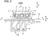
FIG. 2 is a front view of the terminal block according to the embodiment, -
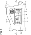
FIG. 3 is a plan view of the terminal block according to the embodiment, -
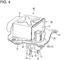
FIG. 4 is a perspective view showing a state where a shielding shell is mounted on the terminal block according to the embodiment, -
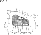
FIG. 5 is a section along V-V ofFIG. 2 , -
FIG. 6 is a section along VI-VI ofFIG. 3 , -
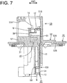
FIG. 7 is a section along VII-VII ofFIG. 2 , -
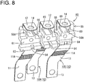
FIG. 8 is a perspective view showing a state where three cores are arranged in contact, -
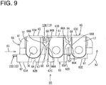
FIG. 9 is a plan view showing the state where the three cores are arranged in contact, -
FIG. 10 is a plan view showing a state where the three cores are arranged while being spaced apart, -
FIG. 11 is a side view of the left core, -
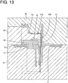
FIG. 12 is a section showing a state where the cores are held by upper and lower dies and a slide die, and -
FIG. 13 is a section showing a state where a secondary molded portion is formed in the upper and lower dies and the slide die. - One particular embodiment of the present invention is described with reference to
FIGS. 1 to 13 . - In this embodiment, a terminal block to be attached to a metal motor case (not shown) housing a motor (as an example of a "device") inside is illustrated as an example of a device connector. As shown in
FIG. 1 , this terminal block includes ametal plate 30 to be attached and fixed to the motor case, a connector housing 50 molded to be integral to themetal plate 30, and one or more (e.g. three)conductive plates 10 held in theconnector housing 50 while penetrating through themetal plate 30 in a plate thickness direction TD. Note that the connector housing 50 particularly corresponds to a molded resin portion and the one or moreconductive plates 10 particularly correspond to conductors. - One or more one ends (first ends) of the
conductive plates 10 are to be connected (particularly bolt-fastened) to one or more, particularly a plurality of unillustrated device-side busbars provided in or at the motor case for electrical connection. On the other hand, in a power supply device for supplying power such as an inverter, one or more, particularly a plurality of wires are arranged to substantially extend toward the motor case and an unillustrated wire-side connector is provided at end portions of these one or more wires. One or more wire-side terminals connected to respective wire ends are provided in this wire-side connector, and these one or more wire-side terminals are connected (particularly bolt-fastened) to the one or more other ends of the respectiveconductive plates 10 for electrical connection. Note that, in the following description, a vertical direction VD is a vertical direction inFIG. 2 and a lateral direction LD is a lateral direction inFIG. 2 . - The (particularly each)
conductive plate 10 is formed by, after a conductive (particularly metal) plate with good electrical conductivity is punched or cut into a specified (predetermined or predeterminable) shape particularly by a press, performing a specified (predetermined or predeterminable) bending process on the punched or cut conductive (metal) plate as shown inFIG. 7 . Theconductive plate 10 includes a terminalmain portion 11 constituting or forming part of a main part of theconductive plate 10, at lest one wire-side fastening portion 12 (as an example of a "fastening portion") substantially extending laterally or forward from the lateral or upper end of the terminalmain portion 11, and at least one device-side fastening portion 13 provided at a lower end portion of the terminal main portion. The terminalmain portion 11 particularly is formed to be longer than the wire-side fastening portion 12. - As shown in
FIG. 2 , the plurality of (e.g. three)conductive plates 10 particularly are arranged substantially side by side in the lateral direction. Further, the terminalmain portions 11 particularly are slightly cranked in the lateral direction LD at intermediate positions. The wire-side fastening portions 12 and the device-side fastening portions 13 are each formed with abolt insertion hole 14 through which an unillustrated fastening bolt is at least partly insertable. - The terminal
main portion 11 of theconductive plate 10A (particularly arranged in the center or intermediate position out of the three conductive plates 10) substantially extends in the vertical direction VD and/or is substantially flat as shown inFIG. 7 . As shown inFIG. 11 , the lateral terminalmain portions 11, 11 (preferably of the bothconductive plates portion 15 bent forward to face the wire-side fastening portion 12 at an intermediate part (particularly at a substantially vertically central part) of the terminalmain portion 11, and the front end of this foldedportion 15 is bent downward particularly substantially at the same position as the front end of the wire-side fastening portion 12. - The
metal plate 30 particularly is made of a metal flat plate material as a base material and includes anopening 31 formed to penetrate in a plate thickness direction TD of the plate material. Theconnector housing 50 includes a wire-sidefitting portion 51 arranged to vertically penetrate through theopening 31, molded to be integral to themetal plate 30 and arranged above themetal plate 30, a (particularly substantially plate-like) flange 52 arranged at the height position of themetal plate 30 and bulging out sideways, and a device-sidefitting portion 53 arranged below themetal plate 30. - As shown in
FIG. 1 , the wire-sidefitting portion 51 particularly substantially is in the form of a box long in the lateral direction and includes a front end opening 51 A (as a particular first opening) which is open in one direction (e.g. forward) and an upper end opening 51 B (as a particular second opening) which is open in another direction (e.g. upward). The unillustrated wire-side connector is at least partly fittable or insertable into the wire-sidefitting portion 51 through the front end opening 51 A of the wire-sidefitting portion 51. - As shown in
FIG. 2 , one or more (e.g. three)nut accommodating portions 55 are formed (particularly substantially side by side in the lateral direction LD) in the wire-sidefitting portion 51. These one or more (e.g. three)nut accommodating portions 55 are respectively open to two sides such as forward and upward. Further, all the threenut accommodating portions 55 is/are arranged to substantially face (particularly forward) through the front or first end opening 51 A and substantially face (particularly upward) through the upper or second end opening 51 B. One or more nuts N press-fitted through the front end opening 51A from front particularly are so accommodated in thenut accommodating portions 55 that the axis lines of the nuts N are aligned with the vertical direction VD. - The wire-
side fastening portions 12 of theconductive plates 10 are arranged to close the upper end openings of thenut accommodating portions 55 as shown inFIGS. 1 and2 . Further, as shown inFIG. 7 , eachconductive plate 10 is arranged to penetrate through theopening 31 in the vertical direction VD and so held in theconnector housing 50 that the wire-side fastening portion 12 is substantially arranged around thebolt insertion hole 14 and at least partly exposed forward and/or upward in the wire-sidefitting portion 51 and, on the other hand, the device-side fastening portion 13 is substantially arranged around thebolt insertion hole 14 and at least partly exposed backward at the lower end portion of the device-sidefitting portion 53. Each wire-side fastening portion 12 is at least partly exposed to the outside through the upper end opening 51 B of the wire-sidefitting portion 51. That is, the upper end opening 51 B of the wire-sidefitting portion 51 particularly is or may be used as a service hole used to at least partly insert a tool or the like for a bolt fastening operation. The wire-side terminal is substantially placed on the wire-side fastening portion 12 and the tool is inserted inside through the upper end opening 51 B to threadably engage the fastening bolt with the nut N, whereby theconductive plate 10 and the wire-side terminal are electrically connected. Note that an unillustrated service cover is mounted on or to the upper end opening 51 B of the wire-sidefitting portion 51 after bolt fastening, thereby closing the upper end opening 51 B. - An escaping
recess 56 for allowing a leading end part of the fastening bolt penetrating through the nut N to escape when the fastening bolt is fastened to the nut N is provided below eachnut accommodating portion 55. The escapingrecess 56 particularly is formed to be narrower than thenut accommodating portion 55 in the lateral direction LD and integrally or unitarily formed with thenut accommodating portion 55 by a slide die 92 to be described later. - As shown in
FIG. 4 , ametal shielding shell 80 at least partly covering the wire-sidefitting portion 51 except the rear surface is mounted on the wire-sidefitting portion 51. This shieldingshell 80 is formed by, after a conductive (particularly metal) plate with good electrical conductivity is punched or cut into a specified (predetermined or predeterminable) shape particularly by a press, performing a specified (predetermined or predeterminable) bending process on the punched or cut conductive (metal) plate. The shieldingshell 80 includes a (particularly braided) fixingportion 81 having a laterally long cylindrical shape and adapted to crimp a braided wire, which is provided to collectively cover shielded conductive paths of the wire-side connector, against a crimp ring, and a fixingpiece 82 for fixing the shieldingshell 80 to themetal plate 30 and electrically connecting the shieldingshell 80 and themetal plate 30. - Since the
flange 52 particularly is formed to be integral to themetal plate 30 in a range not reaching an outer peripheral edge portion of themetal plate 30, the outer peripheral edge portion of themetal plate 30 particularly is exposed. Further, a wire-side flange 52A at a side of the wire-sidefitting portion 51 is formed to extend in the lateral direction LD and backward direction, and a device-side flange 52B at a side of the device-sidefitting portion 53 is formed to substantially cover a surface of themetal plate 30 at the side of the device-sidefitting portion 53. - The
opening 31 particularly has a substantially trapezoidal shape. Further, the foldedportions 15 of theconductive plates 10 at the lateral (left and/or right) side(s) particularly out of the threeconductive plates 10 are arranged in theopening 31. On the other hand, athick portion 57 as a thick resin layer is formed particularly from a lower end portion of the wire-sidefitting portion 51 to an upper end portion of the device-sidefitting portion 53 as shown inFIGS. 5 to 7 . That is, the one or more (e.g. three)conductive plates 10 having a complicated shape are arranged to penetrate through theopening 31 of themetal plate 30 in thisthick portion 57. - Further, one or more, particularly a plurality of mounting
holes 32 are formed in the outer peripheral edge portion of themetal plate 30. Unillustrated one or more fixing bolts or rivets are at least partly inserted through these mountingholes 32 and fastened to the motor case, whereby the terminal block can be attached and fixed to the motor case. - The device-side
fitting portion 53 is housed into the motor case when the terminal block is fixed to the motor case. Further, as shown inFIG. 1 , one or more (e.g. three)nut accommodating portions 58 are formed in the device-sidefitting portion 53. Specifically, out of thesenut accommodating portions 58, thenut accommodating portion 58 located in the center or at an intermediate position is arranged behind the other nutaccommodating portions 58. In thenut accommodating portions 58 of the device-sidefitting portion 53, the fastening bolts are threadably engaged with respective nuts N to electrically connect theconductive plates 10 and the device-side busbars similar to thenut accommodating portions 55 of the wire-sidefitting portion 51. In this way, the wire-side terminals and the device-side busbars are electrically connected using theconductive plates 10 as intermediate terminals. - The
connector housing 50 particularly is composed of a primary moldedportion 61 made e.g. of synthetic resin and molded to be integral or unitary to the one or more (e.g. three)conductive plates 10 by primary molding and a secondary moldedportion 70 made e.g. of synthetic resin and molded to be integral or unitary to the primary moldedportion 61 by secondary molding, and particularly formed in two separate processes. - A primary molded
article 60 formed by primary molding is composed of or comprises the one or more (e.g. three)conductive plates 10 and the primary moldedportion 61 made of synthetic resin and covering parts of the terminalmain portions 11 of the (three) conductive plate(s) 10. As shown inFIGS. 8 and9 , the (three) conductive plate(s) 10 is/are held in the primary moldedportion 61 while particularly being arranged at equal intervals in the lateral direction. - As shown in
FIG. 8 , the primary moldedportion 61 particularly is roughly in the form of a block having a substantially rectangular shape longer in the lateral direction LD when viewed from above, and at least partly covers substantially vertical central or intermediate parts of the terminalmain portions 11 of the respective conductive plates 10 (particularly substantially over the entire circumference). The terminalmain portion 11 of theconductive plate 10A located in the center or intermediate position is covered while vertically penetrating through a rear part of the primary moldedportion 61, and the terminalmain portions 11 of theconductive plates 10B located at the lateral (left and/or right) side(s) is/are covered in the rear part of the primary moldedportion 61 and the folding portion(s) 15 thereof is/are covered in a lower part of the primary moldedportion 61 as shown inFIG. 11 . In other words, as shown inFIGS. 1 and11 , the primary moldedportion 61 particularly at least partly covers cranked parts of the terminalmain portions 11 of the respectiveconductive plates 10, and these covered parts are subject to an injection pressure of molding resin injected from the lateral (e.g. left) side. Note that one ormore sealing portions 11 A where an adhesive is to be applied are provided below the parts of the terminalmain portions 11 of the respectiveconductive plates 10 covered by the primary moldedportion 61 and/or adhere to the secondary moldedportion 70 to prevent the entrance of water or the like into theconnector housing 50 when the secondary moldedportion 70 is formed. - Further, one or more
resin entering spaces 64 into which molding resin can at least partly enter when the secondary moldedportion 70 is formed are formed to extend in forward and backward directions FBD (directions crossing an arrangement direction AD of the conductive plates 10) in afront end surface 62 and arear end surface 63 of the primary moldedportion 61 extending (particularly substantially straight) in the lateral direction LD as shown inFIGS. 9 and10 . Theseresin entering spaces 64 particularly have each a substantially rectangular plan view and/or are at least partly formed between the adjacentconductive plates 10 in the primary moldedportion 61, in a part corresponding to the leftconductive plate 10B in the primary moldedportion 61 and/or in a part corresponding to theconductive plate 10A located in the center or intermediate position in the front end surface of the primary moldedportion 61. Further, theresin entering spaces 64 provided between the adjacentconductive plates 10 particularly are formed to be longer in forward and backward directions FBD than theresin entering spaces 64 provided in correspondence with theconductive plates 10. Theresin entering spaces 64 at least partly provided between the adjacentconductive plates 10 are so formed that intermediate or substantially central parts (contact portions 66) of the primary moldedportion 61 in forward and backward directions FBD particularly are left at the back ends of theresin entering spaces 64. That is, a straight part of thefront end surface 62 of the primary moldedarticle 60 substantially extending in the lateral direction LD is divided by theresin entering spaces 64 as shown inFIG. 9 , with the result that thefront end surface 62 is composed ofstraight parts straight parts front end surface 62 of the primary moldedarticle 60 is not divided by theresin entering spaces 64. - Similar to the
front end surface 62, a substantially straight part of therear end surface 63 of the primary moldedarticle 60 substantially extending in the lateral direction LD particularly is also divided by theresin entering spaces 64, with the result that therear end surface 63 is composed of substantiallystraight parts straight parts rear end surface 63 of the primary moldedarticle 60 is not divided by theresin entering spaces 64. - Further, as shown in
FIG. 9 , two or more (e.g. three)cores article 60. - The
respective cores resin entering spaces 64 provided between the adjacentconductive plates adjacent cores contact portion 66 formed at the back ends of theresin entering spaces 64. In other words, theadjacent cores contact portion 66. - The
contact portion 66 is composed of or comprises afirst linking portion 67 substantially extending laterally (e.g. to the right) from the primary moldedportion 61 of the core 65 located on the lateral (left) side and asecond linking portion 68 substantially extending laterally (e.g. to the left) from the primary moldedportion 61 of the core 65 located on the opposite lateral (right) side. - The
respective linking portions first surfaces first surfaces 66A, and the twofirst surfaces second surface 66B particularly are connected in a cranked manner. The twofirst surfaces portion 67 and the twofirst surfaces portion 68 particularly are in surface contact in the injection direction, and/or thesecond surface 66B of the linkingportion 67 and thesecond surface 66B of the linkingportion 68 particularly are in surface contact in a direction at an angle different from 0° or 180°, preferably substantially perpendicular to the injection direction. That is, parts of therespective linking portions surfaces 66A and thesecond surface 66B as shown inFIG. 9 , and theadjacent cores - One or more, particularly a pair of tightly holding
portions 69, 69 (particularly substantially facing each other in the lateral direction LD and) standing upward are provided on the top of each core 65 as shown inFIG. 8 . The (pairs of) tightly holding portion(s) 69 substantially extend(s) in forward and backward directions FBD, and tightly hold(s) the slide die 92 for forming thenut accommodating portions 55 and the escapingrecesses 56 of the connector housing 50 (particularly from substantially opposite lateral sides) when secondary molding is performed. Abottom wall 56A connecting the lower ends of the tightly holdingportions portions bottom walls 56A to the wire-side fastening portions 12 arranged above thenut accommodating portions 55 particularly is set to be substantially equal to a length which is the sum of the heights of thenut accommodating portions 55 and the escapingrecesses 56 in theconnector housing 50, and/or the wire-side fastening portions 12 and thebottom walls 56A tightly hold the slide die 92 from opposite upper and lower sides when secondary molding is performed. - The secondary molded
portion 70 formed by secondary molding is such that the primary moldedportion 61 of the primary moldedarticle 60 penetrates through theopening 31 of themetal plate 30 in forward and backward directions FBD as shown inFIGS. 5 and6 , and/or constitutes or forms part of theabove connector housing 50 together with the primary moldedportion 61. At the time of secondary molding, molten molding resin to be molded into the secondary moldedportion 70 at least partly enters theresin entering spaces 64 of the primary moldedarticle 60 and substantially flows to the both upper and lower surfaces of themetal plate 30, whereby the primary moldedarticle 60 and themetal plate 30 are integrally formed. That is, the formation of voids in thethick portion 57 of theconnector housing 50 is suppressed or reduced by arranging the primary moldedportion 61 of the primary moldedarticle 60 in thethick portion 57 of theconnector housing 50 and forming thethick portion 57, which is thickest in theconnector housing 50, in the primary moldedportion 61 and the secondary moldedportion 70. This can prevent crack formation in thethick portion 57 due to voids and a reduction in the waterproof property of the terminal block. Further, since the primary moldedarticle 60 particularly is formed as three separate parts for the respectiveconductive plates 10, the formation of voids in the primary moldedportion 61 can be further suppressed. - The terminal block of this embodiment is structured as described above. Next, a production method of the secondary molded
portion 70 and functions and effects thereof are described. - First, the
respective cores lower die 91 of first and second (upper and lower) dies 90, 91, which are opened (particularly substantially in the vertical direction VD) for secondary molding, while being held in surface contact at therespective contact portions 66. At this time, since theadjacent cores lower die 91 only by bringing the respective cranked linkingportions cores 65 in thelower die 91 can be simplified as compared with the case where the linking portions are engaged with each other such as by mating engagement. Further, as compared with the case where therespective linking portions portion 61 can be simplified and production cost of the die for primary molding can be reduced. - When all the
cores 65 are set in thelower die 91, the slide die 92 is inserted from front into spaces substantially enclosed by the pairs of tightly holdingportions respective cores side fastening portions 12 and thebottom walls 56A and the die is so clamped that the upper and lower dies 90, 91 particularly sandwich all thecores 65 from the upper and lower sides as shown inFIG. 13 . At this time, the slide die 92 is so assembled as to be tightly held from the lateral (left and right) sides by the one or more, particularly the pairs of tightly holdingportions side fastening portions 12 and thebottom walls 56A. Specifically, as shown inFIGS. 12 and13 , the slide die 92 includes one or more (e.g. three) molding pins 93 each composed of or comprising a nut accommodatingportion forming portion 93A and an escapingrecess forming portion 93B narrower than the nut accommodatingportion forming portion 93A in the lateral direction LD and the escapingrecess forming portions 93B particularly are tightly held from the lateral (left and/or right) sides by the pairs of the tightly holdingportions portion 61. - Subsequently, the secondary molded
portion 70 is formed by injecting molten molding resin, for example, from the back side to the front side of the plane ofFIG. 13 from an unillustrated gate provided at a lateral side of the upper and lower dies 90, 91, thereby forming theconnector housing 50 as shown inFIG. 13 . At this time, the molding resin particularly is received by the left surface of the primary moldedportion 61 in therespective cores respective cores conductive plates 10 as shown inFIG. 9 . However, since therespective cores cores 65 become integral, thereby resisting the injection pressure of the molding resin and suppressing displacements of therespective cores conductive plates 10 and suppress displacements of therespective cores - Further, since the
respective cores portions side fastening portions 12 and thebottom walls 56A, displacements of therespective cores conductive plates 10 resulting from displacements of therespective cores portions respective cores portion 61 form pairs ofinner walls recesses 56 of theconnector housing 50 together with the secondary moldedportion 70 as shown inFIG. 6 . - The secondary molded
portion 70 formed as described above is cured by being cooled, and forms theconnector housing 50 together with the primary moldedportion 61. In this cooling process, the secondary moldedportion 70 is cured and shrinks to squash the part of the primary moldedportion 61 covered thereby. However, in this embodiment, the straight parts of the front and rear end surfaces 62, 63 of the primary moldedportion 61 particularly are divided by theresin entering spaces 64, and the lengths of the parts of the secondary moldedportion 70 individually covering the respectivestraight parts respective cores 65 are short. Thus, as compared with the case where the primary molded portion is formed with noresin entering spaces 64, the amount of shrinkage of the secondary moldedportion 70 individually covering the respectivestraight parts respective cores portion 61 by the secondary moldedportion 70 can be suppressed. Further, since theresin entering spaces 64 substantially extending in forward and backward directions FBD particularly are formed to be larger between theadjacent cores portion 61 and further suppress the influence of cure shrinkage in the secondary moldedportion 70. - Further, since the escaping
recess forming portions 93B of the slide die 92 particularly are tightly held by the pairs of tightly holdingportions portion 70 in this embodiment, the width of the primary moldedportion 61 in the lateral direction LD can be shortened and the thickening of the primary moldedportion 61 in the lateral direction LD can be suppressed as compared with the case where pairs of tightly holding portions for tightly holding the nut accommodatingportion forming portions 93A for forming thenut accommodating portions 55 are provided. This can further suppress the formation of voids in the primary moldedportion 61. - Accordingly, to suppress the formation of a molded resin portion with a primary molded article inclined and suppress the formation of voids in the molded resin portion, a terminal block in which one or more, particularly a plurality of terminals or (particularly metal)
conductive plates 10 to be connected to respective device-side terminals or busbars provided in a device such as a motor are made integral by aconnector housing 50 includes a primary moldedarticle 60 in which the one or more, particularly the plurality of terminals orconductive plates 10 are made integral by aconnector housing 50; ametal plate 30 to be attached and fixed to a motor case; and a secondary moldedportion 70 integrally forming the primary moldedarticle 60 and themetal plate 30. The secondary moldedportion 70 is formed by a secondary molding die including both upper and lower dies 90, 91 and aslide die 92. Pairs of tightly holdingportions portion 61 before the secondary moldedportion 70 is formed. - The present invention is not limited to the above described and illustrated embodiment. For example, the following embodiments are also included in the technical scope of the present invention.
- (1) Although the primary molded
article 60 is divided into the threecores 65 in the above embodiment, the present invention is not limited to such a mode. For example, the primary moldedarticle 60 may not be divided. - (2) Although the terminal block includes the shielding
shell 80 in the above embodiment, the present invention is not limited to such a mode. For example, the present invention may be applied to a terminal block which requires no shielding shell. - (3) Although the
connector housing 50 is formed with the primary moldedportion 61 penetrating through theopening 31 of themetal plate 30 in the above embodiment, the present invention is not limited to such a mode. For example, the primary moldedportion 61 may not penetrate through theopening 31 of themetal plate 30. - (4) Although the three cores are held in contact in the lateral direction by the
contact portions 66 in the above embodiment, the present invention is not limited to such a mode. For example, the adjacent cores may be entirely separated by resin entering spaces and may not be in contact. -
- 10:
- conductive plate (conductor)
- 12:
- wire-side fastening portion (fastening portion)
- 30:
- metal plate
- 50:
- connector housing (molded resin portion)
- 55:
- nut accommodating portion
- 56:
- escaping recess
- 56A:
- bottom wall
- 60:
- primary molded article
- 61:
- primary molded portion
- 65:
- core
- 69:
- tightly holding portion
- 70:
- secondary molded portion
- 90:
- lower die
- 91:
- upper die
- 92:
- slide die
- X1:
- injection direction
Claims (14)
- A device connector in which one or more conductors (10) to be connected to device-side terminals provided in a device are made integral by a molded resin portion (50), comprising:a primary molded article (60) in which the one or more conductors (10) are made integral by a primary molded portion (61) made of synthetic resin;a metal plate (30) to be attached and fixed to the device; anda secondary molded portion (70) made of synthetic resin and integrally forming the primary molded article (60) and the metal plate (30);wherein:the molded resin portion (50) comprises the primary molded portion (61) and the secondary molded portion (70);the secondary molded portion (70) is formed by a secondary molding die including both first and second dies (90, 91) which are opened in a first direction (VD) and at least one slide die (92) which is opened in a second direction (FBD) intersecting the first direction (VD); andone or more tightly holding portions (69) arranged to intersect with an injection direction (X1), in which molding resin for forming the secondary molded portion (70) is injected, and adapted to tightly hold the slide die (92) are provided on the primary molded portion (61) before the secondary molded portion (70) is formed.
- A device connector according to claim 1, wherein two tightly holding portions (69) are provided to substantially face each other in the injection direction (X1) on the primary molded portion (61) before the secondary molded portion (70) is formed.
- A device connector according to any one of the preceding claims, wherein at least one nut accommodating portion (55) for at least partly accommodating a nut to be threadably engaged with a fastening bolt to be fastened to the conductor (10) and at least one escaping recess (56) communicating with the nut accommodating portion (55) and adapted to allow the fastening bolt threadably engaged with and penetrating through the nut to escape are formed in the molded resin portion (50) by the slide die (92).
- A device connector according to claim 3, wherein the escaping recess (56) is formed to include the one or more tightly holding portions (69).
- A device connector according to any one of the preceding claims, wherein a fastening portion (12) of the conductor (10) to which the fastening bolt is to be fastened is arranged at the upper end of the nut accommodating portion (55).
- A device connector according to claim 5, wherein the escaping recess (56) includes a bottom wall (56A) connected to the one or more tightly holding portions (69), particularly connecting the pair of tightly holding portions (69); and
the slide die (92) preferably is tightly held from upper and lower sides by the fastening portion (12) of the conductor (10) and the bottom wall (56A). - A device connector according to any one of the preceding claims, wherein the primary molded article (60) is formed such that one or more cores (65) individually formed for the one or more respective conductors (10) are provided preferably arranged substantially side by side in a lateral direction (LD).
- A production method for producing a device connector in which one or more conductors (10) to be connected to device-side terminals provided in a device are made integral by a molded resin portion (50) comprising a primary molded portion (61) and a secondary molded portion (70), comprising the following steps:molding a primary molded article (60) in which the one or more conductors (10) are made integral by a primary molded portion (61) of synthetic resin;molding a secondary molded portion (70) made of synthetic resin to integrally form the primary molded article (60) and a metal plate (30) to be attached and fixed to the device, wherein the secondary molded portion (70) is formed by a secondary molding die including both first and second dies (90, 91) which are opened in a first direction (VD) and at least one slide die (92) which is opened in a second direction (FBD) intersecting the first direction (VD);while tightly holding the slide die (92) by means of one or more tightly holding portions (69) arranged to intersect with an injection direction (X1), in which molding resin for forming the secondary molded portion (70) is injected, and provided on the primary molded portion (61) before the secondary molded portion (70) is formed.
- A method according to claim 8, wherein the slide die (92) is held by means of two tightly holding portions (69) which are provided to substantially face each other in the injection direction (X1) on the primary molded portion (61) before the secondary molded portion (70) is formed.
- A method according to claim 8 or 9, further comprising forming in the molded resin portion (50) by the slide die (92) at least one nut accommodating portion (55) for at least partly accommodating a nut to be threadably engaged with a fastening bolt to be fastened to the conductor (10) and at least one escaping recess (56) communicating with the nut accommodating portion (55) and adapted to allow the fastening bolt threadably engaged with and penetrating through the nut to escape.
- A method according to claim 10, wherein the escaping recess (56) is formed to include the one or more tightly holding portions (69).
- A method according to any one of the preceding claims 8 to 11, wherein a fastening portion (12) of the conductor (10) to which the fastening bolt is to be fastened is formed at the upper end of the nut accommodating portion (55).
- A method according to claim 12, wherein the escaping recess (56) is formed with a bottom wall (56A) connected to the one or more tightly holding portions (69), particularly connecting the pair of tightly holding portions (69); and
the slide die (92) preferably is tightly held from upper and lower sides by the fastening portion (12) of the conductor (10) and the bottom wall (56A). - A method according to any one of the preceding claims 8 to 13, wherein the primary molded article (60) is formed such that one or more cores (65) individually formed for the one or more respective conductors (10) are provided preferably arranged substantially side by side in a lateral direction (LD).
Applications Claiming Priority (1)
| Application Number | Priority Date | Filing Date | Title |
|---|---|---|---|
| JP2011056338A JP5626047B2 (en) | 2011-03-15 | 2011-03-15 | Connector for equipment |
Publications (2)
| Publication Number | Publication Date |
|---|---|
| EP2500995A1 true EP2500995A1 (en) | 2012-09-19 |
| EP2500995B1 EP2500995B1 (en) | 2017-12-27 |
Family
ID=45768114
Family Applications (1)
| Application Number | Title | Priority Date | Filing Date |
|---|---|---|---|
| EP12001106.9A Not-in-force EP2500995B1 (en) | 2011-03-15 | 2012-02-20 | Production method for a connector |
Country Status (4)
| Country | Link |
|---|---|
| US (1) | US8545265B2 (en) |
| EP (1) | EP2500995B1 (en) |
| JP (1) | JP5626047B2 (en) |
| CN (1) | CN102683962B (en) |
Cited By (2)
| Publication number | Priority date | Publication date | Assignee | Title |
|---|---|---|---|---|
| FR3018397A1 (en) * | 2014-03-10 | 2015-09-11 | Valeo Systemes Dessuyage | CONNECTION FRAME AND ASSOCIATED METHOD |
| WO2023222963A1 (en) * | 2022-05-20 | 2023-11-23 | Nidec Psa Emotors | Device for making an electrical connection between an electric motor and an inverter |
Families Citing this family (55)
| Publication number | Priority date | Publication date | Assignee | Title |
|---|---|---|---|---|
| US20050131837A1 (en) | 2003-12-15 | 2005-06-16 | Sanctis Jeanne D. | Method, system and program product for communicating e-commerce content over-the-air to mobile devices |
| US8370269B2 (en) | 2004-06-02 | 2013-02-05 | Overstock.Com, Inc. | System and methods for electronic commerce using personal and business networks |
| US9747622B1 (en) | 2009-03-24 | 2017-08-29 | Overstock.Com, Inc. | Point-and-shoot product lister |
| JP5885013B2 (en) * | 2010-09-22 | 2016-03-15 | 株式会社オートネットワーク技術研究所 | connector |
| JP5569442B2 (en) * | 2011-03-15 | 2014-08-13 | 住友電装株式会社 | Connector for equipment |
| JP5626047B2 (en) * | 2011-03-15 | 2014-11-19 | 住友電装株式会社 | Connector for equipment |
| JP5751875B2 (en) * | 2011-03-22 | 2015-07-22 | 矢崎総業株式会社 | Shield connector |
| US9047642B2 (en) | 2011-03-24 | 2015-06-02 | Overstock.Com, Inc. | Social choice engine |
| JP5909327B2 (en) * | 2011-05-19 | 2016-04-26 | 矢崎総業株式会社 | connector |
| JP5672157B2 (en) * | 2011-06-02 | 2015-02-18 | 株式会社オートネットワーク技術研究所 | Connector and manufacturing method thereof |
| JP5743740B2 (en) * | 2011-06-23 | 2015-07-01 | 矢崎総業株式会社 | connector |
| JP5733573B2 (en) * | 2011-09-05 | 2015-06-10 | 住友電装株式会社 | Connector for equipment |
| JP5926951B2 (en) * | 2011-12-27 | 2016-05-25 | 矢崎総業株式会社 | connector |
| JP5757248B2 (en) * | 2012-01-19 | 2015-07-29 | 住友電装株式会社 | Connector for equipment |
| JP2013229154A (en) * | 2012-04-25 | 2013-11-07 | Hirose Electric Co Ltd | Power supply electrode connection member |
| JP5937944B2 (en) * | 2012-10-05 | 2016-06-22 | ホシデン株式会社 | Mold for molding, method for producing resin molded product using the same, and resin molded product |
| US10546262B2 (en) | 2012-10-19 | 2020-01-28 | Overstock.Com, Inc. | Supply chain management system |
| DE202012011808U1 (en) * | 2012-12-10 | 2014-03-13 | Rosenberger Hochfrequenztechnik Gmbh & Co. Kg | connecting device |
| US11023947B1 (en) | 2013-03-15 | 2021-06-01 | Overstock.Com, Inc. | Generating product recommendations using a blend of collaborative and content-based data |
| US11676192B1 (en) | 2013-03-15 | 2023-06-13 | Overstock.Com, Inc. | Localized sort of ranked product recommendations based on predicted user intent |
| US10810654B1 (en) | 2013-05-06 | 2020-10-20 | Overstock.Com, Inc. | System and method of mapping product attributes between different schemas |
| US9483788B2 (en) | 2013-06-25 | 2016-11-01 | Overstock.Com, Inc. | System and method for graphically building weighted search queries |
| US10929890B2 (en) | 2013-08-15 | 2021-02-23 | Overstock.Com, Inc. | System and method of personalizing online marketing campaigns |
| US10872350B1 (en) | 2013-12-06 | 2020-12-22 | Overstock.Com, Inc. | System and method for optimizing online marketing based upon relative advertisement placement |
| JP6135516B2 (en) * | 2014-01-08 | 2017-05-31 | 住友電装株式会社 | Connector for equipment |
| CN103895158A (en) * | 2014-04-16 | 2014-07-02 | 威猛工业自动化系统(昆山)有限公司 | Device and method for producing power lug with contact pin |
| JP6413799B2 (en) * | 2015-01-28 | 2018-10-31 | 住友電装株式会社 | Connector for equipment |
| JP6492929B2 (en) * | 2015-04-23 | 2019-04-03 | 住友電装株式会社 | connector |
| JP6344320B2 (en) * | 2015-06-17 | 2018-06-20 | 住友電装株式会社 | connector |
| JP6141363B2 (en) * | 2015-07-22 | 2017-06-07 | 住友電装株式会社 | Shield connector |
| KR102455570B1 (en) * | 2015-12-17 | 2022-10-17 | 한국단자공업 주식회사 | Joint apparatus |
| JP6597393B2 (en) * | 2016-02-29 | 2019-10-30 | 住友電装株式会社 | Resin molded product and its manufacturing method |
| JP6536431B2 (en) | 2016-02-29 | 2019-07-03 | 住友電装株式会社 | Resin molding |
| US10534845B2 (en) | 2016-05-11 | 2020-01-14 | Overstock.Com, Inc. | System and method for optimizing electronic document layouts |
| JP6709754B2 (en) * | 2017-05-31 | 2020-06-17 | 矢崎総業株式会社 | Connector housing mounting structure |
| JP6854893B2 (en) | 2017-07-07 | 2021-04-07 | 日立Astemo株式会社 | Manufacturing method of connector molded body, electronic control device and connector molded body |
| JP6874654B2 (en) * | 2017-11-22 | 2021-05-19 | 住友電装株式会社 | Connector and its manufacturing method |
| US10808657B2 (en) * | 2018-02-02 | 2020-10-20 | Ford Global Technologies, Llc | Vehicle component with an accessory mounting feature and a method and tool for forming |
| JP6756764B2 (en) * | 2018-03-30 | 2020-09-16 | 矢崎総業株式会社 | Busbar parts, terminal blocks and in-vehicle equipment |
| JP6951669B2 (en) * | 2018-06-04 | 2021-10-20 | 株式会社オートネットワーク技術研究所 | Connector and connector device |
| JP7004169B2 (en) * | 2018-06-19 | 2022-01-21 | 住友電装株式会社 | Caps and connecting devices |
| US11152833B2 (en) * | 2018-07-23 | 2021-10-19 | Borgwarner Inc. | Electrical device having compact connector assembly suited for high power applications |
| KR20200035665A (en) * | 2018-09-27 | 2020-04-06 | 현대모비스 주식회사 | Block terminal for motor and manufacturing method thereof |
| JP7077928B2 (en) * | 2018-12-06 | 2022-05-31 | 住友電装株式会社 | Connector and its manufacturing method |
| JP7087989B2 (en) * | 2018-12-25 | 2022-06-21 | 住友電装株式会社 | Aperture closure device for the case |
| JP7063286B2 (en) * | 2019-02-11 | 2022-05-09 | 住友電装株式会社 | connector |
| JP7115349B2 (en) * | 2019-02-11 | 2022-08-09 | 住友電装株式会社 | connector |
| US11514493B1 (en) | 2019-03-25 | 2022-11-29 | Overstock.Com, Inc. | System and method for conversational commerce online |
| US11205179B1 (en) | 2019-04-26 | 2021-12-21 | Overstock.Com, Inc. | System, method, and program product for recognizing and rejecting fraudulent purchase attempts in e-commerce |
| JP7151639B2 (en) * | 2019-06-26 | 2022-10-12 | 住友電装株式会社 | connector |
| JP7044744B2 (en) * | 2019-08-23 | 2022-03-30 | 矢崎総業株式会社 | connector |
| US11734368B1 (en) | 2019-09-26 | 2023-08-22 | Overstock.Com, Inc. | System and method for creating a consistent personalized web experience across multiple platforms and channels |
| JP2022130095A (en) * | 2021-02-25 | 2022-09-06 | 住友電装株式会社 | connector |
| US11894729B2 (en) * | 2021-03-13 | 2024-02-06 | Hamilton Sundstrand Corporation | Alternating current connection housing with integrated inserts |
| JP2022161407A (en) * | 2021-04-09 | 2022-10-21 | 株式会社オートネットワーク技術研究所 | Terminal block |
Citations (3)
| Publication number | Priority date | Publication date | Assignee | Title |
|---|---|---|---|---|
| DE10009652A1 (en) * | 1999-03-02 | 2000-09-21 | Yazaki Corp | Molding of housing for enclosing core section of multi-pin plug includes a projection on core that extends to mold wall to indicate any distortion |
| US20080000668A1 (en) * | 2006-06-29 | 2008-01-03 | Sumitomo Wiring Systems, Ltd. | Method for producing a resin molded article, a resin molded product and a molding die therefor |
| JP2009032500A (en) | 2007-07-26 | 2009-02-12 | Sumitomo Wiring Syst Ltd | Equipment connector |
Family Cites Families (59)
| Publication number | Priority date | Publication date | Assignee | Title |
|---|---|---|---|---|
| JP3339300B2 (en) * | 1996-04-23 | 2002-10-28 | 矢崎総業株式会社 | Connector manufacturing method |
| US6270377B1 (en) * | 1998-07-16 | 2001-08-07 | Harness System Technologies Research, Ltd. | Shielding connector |
| EP1133022B1 (en) * | 2000-03-07 | 2008-04-30 | Autonetworks Technologies, Ltd. | Shield connector and terminal connecting device for shielding electric wire |
| US6595789B2 (en) * | 2000-10-20 | 2003-07-22 | Autonetworks Technologies, Ltd. | Electronic unit, shield cable connecting structure, connecting method, wires waterproof-connecting structure, and method |
| JP3846849B2 (en) * | 2001-03-13 | 2006-11-15 | 株式会社オートネットワーク技術研究所 | Terminal connection device |
| JP2002324627A (en) * | 2001-04-25 | 2002-11-08 | Yazaki Corp | Electromagnetic wave shielding structure |
| JP3713528B2 (en) * | 2001-12-26 | 2005-11-09 | 株式会社オートネットワーク技術研究所 | Wire harness for equipment installation |
| US6716071B2 (en) * | 2002-03-05 | 2004-04-06 | Autonetworks Technologies, Ltd. | Molded electrical connector |
| US6655989B1 (en) * | 2002-07-10 | 2003-12-02 | Ford Motor Company | Environmentally sealed electrical connector system |
| JP3966407B2 (en) * | 2002-09-24 | 2007-08-29 | 矢崎総業株式会社 | Electromagnetic wave shield structure with oil-proof water |
| JP2004153891A (en) * | 2002-10-29 | 2004-05-27 | Mitsubishi Electric Corp | Rotary electric machine |
| US6921292B2 (en) * | 2002-11-21 | 2005-07-26 | Autonetworks Technologies, Ltd. | Connector having shielding shell |
| JP2004172476A (en) * | 2002-11-21 | 2004-06-17 | Auto Network Gijutsu Kenkyusho:Kk | Conductive path having shield function |
| JP3947122B2 (en) * | 2003-03-24 | 2007-07-18 | 株式会社オートネットワーク技術研究所 | Wire connection structure to equipment shield case |
| US6821160B2 (en) * | 2003-04-01 | 2004-11-23 | Delphi Technologies, Inc. | High voltage electrical connection |
| JP2004349026A (en) * | 2003-05-20 | 2004-12-09 | Yazaki Corp | Holder and connector |
| JP2005019188A (en) * | 2003-06-26 | 2005-01-20 | Auto Network Gijutsu Kenkyusho:Kk | Connector for apparatus |
| JP2005019319A (en) * | 2003-06-27 | 2005-01-20 | Auto Network Gijutsu Kenkyusho:Kk | Connector for apparatus |
| JP2005019321A (en) * | 2003-06-27 | 2005-01-20 | Auto Network Gijutsu Kenkyusho:Kk | Connector and manufacturing method of connector |
| US7101217B2 (en) * | 2003-10-23 | 2006-09-05 | Autonetworks Technologies, Ltd. | Shield connector |
| JP3997208B2 (en) * | 2004-02-17 | 2007-10-24 | トヨタ自動車株式会社 | Connector fixing structure |
| JP2005235424A (en) * | 2004-02-17 | 2005-09-02 | Yazaki Corp | Electromagnetic wave shield connector |
| US7150631B2 (en) * | 2004-03-22 | 2006-12-19 | General Motors Corporation | Hybrid electro-mechanical transmission wire isolators with threaded inserts |
| JP4189753B2 (en) * | 2004-04-13 | 2008-12-03 | 住友電装株式会社 | Insert molded product and method of manufacturing insert molded product |
| US7645157B2 (en) * | 2005-03-15 | 2010-01-12 | Toyota Jidosha Kabushiki Kaisha | Connector |
| JP4761931B2 (en) * | 2005-10-27 | 2011-08-31 | 矢崎総業株式会社 | Terminal movable connector |
| JP4559369B2 (en) * | 2006-02-03 | 2010-10-06 | 矢崎総業株式会社 | Packing mounting structure |
| JP4849323B2 (en) * | 2006-07-13 | 2012-01-11 | 住友電装株式会社 | Method for manufacturing insert molded product and mold for insert molding |
| JP4955754B2 (en) * | 2007-03-02 | 2012-06-20 | 株式会社オートネットワーク技術研究所 | Shield shell |
| US7393218B1 (en) * | 2007-03-19 | 2008-07-01 | Lear Corporation | Connector assembly with overmolded shielded housing |
| CA2684934A1 (en) * | 2007-05-23 | 2008-11-27 | Tm4 Inc. | Electrical connector |
| JP5119847B2 (en) * | 2007-10-12 | 2013-01-16 | 住友電装株式会社 | connector |
| JP4632320B2 (en) * | 2007-11-09 | 2011-02-16 | 住友電装株式会社 | Connector for equipment |
| JP5077670B2 (en) * | 2007-11-09 | 2012-11-21 | 住友電装株式会社 | Connector for equipment |
| JP4970220B2 (en) * | 2007-11-16 | 2012-07-04 | 矢崎総業株式会社 | Shield connector |
| JP5095446B2 (en) * | 2008-03-05 | 2012-12-12 | 矢崎総業株式会社 | connector |
| JP5046043B2 (en) * | 2008-07-10 | 2012-10-10 | 住友電装株式会社 | connector |
| JP5110384B2 (en) * | 2008-08-07 | 2012-12-26 | 住友電装株式会社 | connector |
| US7637761B1 (en) * | 2008-08-11 | 2009-12-29 | Gm Global Technology Operations, Inc. | Method and apparatus to connect a wiring harness to an electric machine |
| US7597580B1 (en) * | 2008-09-17 | 2009-10-06 | Yazaki North America, Inc. | Connector with terminal motion reduction |
| JP5258098B2 (en) * | 2008-12-24 | 2013-08-07 | 矢崎総業株式会社 | connector |
| JP5206480B2 (en) * | 2009-02-23 | 2013-06-12 | 住友電装株式会社 | Connector device |
| JP5425507B2 (en) * | 2009-03-30 | 2014-02-26 | 矢崎総業株式会社 | Motor cable device and resin parts used for motor cable device |
| JP5425508B2 (en) * | 2009-03-30 | 2014-02-26 | 矢崎総業株式会社 | Motor cable device and cable body manufacturing method of motor cable device |
| JP5417954B2 (en) * | 2009-04-09 | 2014-02-19 | 住友電装株式会社 | Waterproof connector |
| JP2010244975A (en) * | 2009-04-09 | 2010-10-28 | Sumitomo Wiring Syst Ltd | Connector |
| JP5240522B2 (en) * | 2009-04-13 | 2013-07-17 | 住友電装株式会社 | connector |
| JP5169990B2 (en) * | 2009-05-21 | 2013-03-27 | 住友電装株式会社 | Device connector manufacturing method |
| WO2011007385A1 (en) * | 2009-07-14 | 2011-01-20 | 三菱電機株式会社 | Vehicle condition detection device and method for manufacturing the same |
| JP5333030B2 (en) * | 2009-08-10 | 2013-11-06 | 住友電装株式会社 | Connector manufacturing method |
| JP5233959B2 (en) * | 2009-11-05 | 2013-07-10 | 住友電装株式会社 | Connector for equipment |
| JP5251840B2 (en) * | 2009-11-17 | 2013-07-31 | 住友電装株式会社 | Connector for equipment |
| JP4832581B2 (en) * | 2010-01-29 | 2011-12-07 | トヨタ自動車株式会社 | Terminal block for rotating electrical machines |
| JP5833300B2 (en) * | 2010-11-11 | 2015-12-16 | 矢崎総業株式会社 | connector |
| JP5641346B2 (en) * | 2011-03-15 | 2014-12-17 | 住友電装株式会社 | Shield shell mounting structure |
| JP5640837B2 (en) * | 2011-03-15 | 2014-12-17 | 住友電装株式会社 | Connector for equipment |
| JP5626047B2 (en) * | 2011-03-15 | 2014-11-19 | 住友電装株式会社 | Connector for equipment |
| JP5569442B2 (en) * | 2011-03-15 | 2014-08-13 | 住友電装株式会社 | Connector for equipment |
| JP5641345B2 (en) * | 2011-03-15 | 2014-12-17 | 住友電装株式会社 | Connector for equipment |
-
2011
- 2011-03-15 JP JP2011056338A patent/JP5626047B2/en active Active
-
2012
- 2012-02-20 EP EP12001106.9A patent/EP2500995B1/en not_active Not-in-force
- 2012-03-09 CN CN201210061048.4A patent/CN102683962B/en not_active Expired - Fee Related
- 2012-03-12 US US13/417,885 patent/US8545265B2/en not_active Expired - Fee Related
Patent Citations (3)
| Publication number | Priority date | Publication date | Assignee | Title |
|---|---|---|---|---|
| DE10009652A1 (en) * | 1999-03-02 | 2000-09-21 | Yazaki Corp | Molding of housing for enclosing core section of multi-pin plug includes a projection on core that extends to mold wall to indicate any distortion |
| US20080000668A1 (en) * | 2006-06-29 | 2008-01-03 | Sumitomo Wiring Systems, Ltd. | Method for producing a resin molded article, a resin molded product and a molding die therefor |
| JP2009032500A (en) | 2007-07-26 | 2009-02-12 | Sumitomo Wiring Syst Ltd | Equipment connector |
Cited By (3)
| Publication number | Priority date | Publication date | Assignee | Title |
|---|---|---|---|---|
| FR3018397A1 (en) * | 2014-03-10 | 2015-09-11 | Valeo Systemes Dessuyage | CONNECTION FRAME AND ASSOCIATED METHOD |
| WO2023222963A1 (en) * | 2022-05-20 | 2023-11-23 | Nidec Psa Emotors | Device for making an electrical connection between an electric motor and an inverter |
| FR3135866A1 (en) * | 2022-05-20 | 2023-11-24 | Nidec Psa Emotors | Electrical connection device between an electric motor and an inverter |
Also Published As
| Publication number | Publication date |
|---|---|
| EP2500995B1 (en) | 2017-12-27 |
| CN102683962A (en) | 2012-09-19 |
| JP5626047B2 (en) | 2014-11-19 |
| US8545265B2 (en) | 2013-10-01 |
| US20120238150A1 (en) | 2012-09-20 |
| JP2012195069A (en) | 2012-10-11 |
| CN102683962B (en) | 2015-06-17 |
Similar Documents
| Publication | Publication Date | Title |
|---|---|---|
| EP2500995B1 (en) | Production method for a connector | |
| EP2500985B1 (en) | Device connector and production method therefor | |
| EP2500997B1 (en) | Connector and method of producing it | |
| EP2500996B1 (en) | Device connector and method of producing it | |
| EP2500991B1 (en) | Mounting structure for shielding shell and mounting method therefor | |
| US7268300B2 (en) | Connector for inverter | |
| US8721367B2 (en) | Fuse unit | |
| EP2479852B1 (en) | Insulating plate, insulating plate manufacturing method and terminal block | |
| EP2479845B1 (en) | Terminal block and terminal block manufacturing method | |
| EP2495829A1 (en) | Terminal block and method of molding it | |
| EP2798705B1 (en) | Connector | |
| KR20130031224A (en) | Connector and method of assembling it | |
| JP5821804B2 (en) | Terminal block and method of manufacturing terminal block | |
| JP2004242472A (en) | Conductive path | |
| US11152720B2 (en) | Terminal-equipped wire and wire harness | |
| US10811931B2 (en) | Electrical connection arrangement and method for production thereof | |
| JP2022080937A (en) | Terminal part insulation structure and electric connection box | |
| CN109301674A (en) | For manufacturing the method and adapted to injection system of conductor rail complex |
Legal Events
| Date | Code | Title | Description |
|---|---|---|---|
| PUAI | Public reference made under article 153(3) epc to a published international application that has entered the european phase |
Free format text: ORIGINAL CODE: 0009012 |
|
| AK | Designated contracting states |
Kind code of ref document: A1 Designated state(s): AL AT BE BG CH CY CZ DE DK EE ES FI FR GB GR HR HU IE IS IT LI LT LU LV MC MK MT NL NO PL PT RO RS SE SI SK SM TR |
|
| AX | Request for extension of the european patent |
Extension state: BA ME |
|
| 17P | Request for examination filed |
Effective date: 20130314 |
|
| 17Q | First examination report despatched |
Effective date: 20150706 |
|
| RIC1 | Information provided on ipc code assigned before grant |
Ipc: B29L 31/36 20060101ALN20170629BHEP Ipc: H01R 43/24 20060101ALI20170629BHEP Ipc: H01R 43/18 20060101AFI20170629BHEP Ipc: B29C 45/14 20060101ALI20170629BHEP Ipc: B29C 45/33 20060101ALI20170629BHEP Ipc: H01R 13/504 20060101ALI20170629BHEP |
|
| GRAP | Despatch of communication of intention to grant a patent |
Free format text: ORIGINAL CODE: EPIDOSNIGR1 |
|
| INTG | Intention to grant announced |
Effective date: 20170814 |
|
| GRAS | Grant fee paid |
Free format text: ORIGINAL CODE: EPIDOSNIGR3 |
|
| GRAA | (expected) grant |
Free format text: ORIGINAL CODE: 0009210 |
|
| AK | Designated contracting states |
Kind code of ref document: B1 Designated state(s): AL AT BE BG CH CY CZ DE DK EE ES FI FR GB GR HR HU IE IS IT LI LT LU LV MC MK MT NL NO PL PT RO RS SE SI SK SM TR |
|
| REG | Reference to a national code |
Ref country code: GB Ref legal event code: FG4D |
|
| REG | Reference to a national code |
Ref country code: CH Ref legal event code: EP |
|
| REG | Reference to a national code |
Ref country code: AT Ref legal event code: REF Ref document number: 959068 Country of ref document: AT Kind code of ref document: T Effective date: 20180115 |
|
| REG | Reference to a national code |
Ref country code: IE Ref legal event code: FG4D |
|
| REG | Reference to a national code |
Ref country code: DE Ref legal event code: R096 Ref document number: 602012041265 Country of ref document: DE |
|
| PG25 | Lapsed in a contracting state [announced via postgrant information from national office to epo] |
Ref country code: FI Free format text: LAPSE BECAUSE OF FAILURE TO SUBMIT A TRANSLATION OF THE DESCRIPTION OR TO PAY THE FEE WITHIN THE PRESCRIBED TIME-LIMIT Effective date: 20171227 Ref country code: LT Free format text: LAPSE BECAUSE OF FAILURE TO SUBMIT A TRANSLATION OF THE DESCRIPTION OR TO PAY THE FEE WITHIN THE PRESCRIBED TIME-LIMIT Effective date: 20171227 Ref country code: NO Free format text: LAPSE BECAUSE OF FAILURE TO SUBMIT A TRANSLATION OF THE DESCRIPTION OR TO PAY THE FEE WITHIN THE PRESCRIBED TIME-LIMIT Effective date: 20180327 |
|
| REG | Reference to a national code |
Ref country code: NL Ref legal event code: MP Effective date: 20171227 |
|
| REG | Reference to a national code |
Ref country code: LT Ref legal event code: MG4D |
|
| REG | Reference to a national code |
Ref country code: AT Ref legal event code: MK05 Ref document number: 959068 Country of ref document: AT Kind code of ref document: T Effective date: 20171227 |
|
| PG25 | Lapsed in a contracting state [announced via postgrant information from national office to epo] |
Ref country code: GR Free format text: LAPSE BECAUSE OF FAILURE TO SUBMIT A TRANSLATION OF THE DESCRIPTION OR TO PAY THE FEE WITHIN THE PRESCRIBED TIME-LIMIT Effective date: 20180328 Ref country code: BG Free format text: LAPSE BECAUSE OF FAILURE TO SUBMIT A TRANSLATION OF THE DESCRIPTION OR TO PAY THE FEE WITHIN THE PRESCRIBED TIME-LIMIT Effective date: 20180327 Ref country code: HR Free format text: LAPSE BECAUSE OF FAILURE TO SUBMIT A TRANSLATION OF THE DESCRIPTION OR TO PAY THE FEE WITHIN THE PRESCRIBED TIME-LIMIT Effective date: 20171227 Ref country code: RS Free format text: LAPSE BECAUSE OF FAILURE TO SUBMIT A TRANSLATION OF THE DESCRIPTION OR TO PAY THE FEE WITHIN THE PRESCRIBED TIME-LIMIT Effective date: 20171227 Ref country code: LV Free format text: LAPSE BECAUSE OF FAILURE TO SUBMIT A TRANSLATION OF THE DESCRIPTION OR TO PAY THE FEE WITHIN THE PRESCRIBED TIME-LIMIT Effective date: 20171227 |
|
| PG25 | Lapsed in a contracting state [announced via postgrant information from national office to epo] |
Ref country code: NL Free format text: LAPSE BECAUSE OF FAILURE TO SUBMIT A TRANSLATION OF THE DESCRIPTION OR TO PAY THE FEE WITHIN THE PRESCRIBED TIME-LIMIT Effective date: 20171227 |
|
| PG25 | Lapsed in a contracting state [announced via postgrant information from national office to epo] |
Ref country code: ES Free format text: LAPSE BECAUSE OF FAILURE TO SUBMIT A TRANSLATION OF THE DESCRIPTION OR TO PAY THE FEE WITHIN THE PRESCRIBED TIME-LIMIT Effective date: 20171227 Ref country code: CZ Free format text: LAPSE BECAUSE OF FAILURE TO SUBMIT A TRANSLATION OF THE DESCRIPTION OR TO PAY THE FEE WITHIN THE PRESCRIBED TIME-LIMIT Effective date: 20171227 Ref country code: SK Free format text: LAPSE BECAUSE OF FAILURE TO SUBMIT A TRANSLATION OF THE DESCRIPTION OR TO PAY THE FEE WITHIN THE PRESCRIBED TIME-LIMIT Effective date: 20171227 Ref country code: CY Free format text: LAPSE BECAUSE OF FAILURE TO SUBMIT A TRANSLATION OF THE DESCRIPTION OR TO PAY THE FEE WITHIN THE PRESCRIBED TIME-LIMIT Effective date: 20171227 Ref country code: EE Free format text: LAPSE BECAUSE OF FAILURE TO SUBMIT A TRANSLATION OF THE DESCRIPTION OR TO PAY THE FEE WITHIN THE PRESCRIBED TIME-LIMIT Effective date: 20171227 |
|
| PG25 | Lapsed in a contracting state [announced via postgrant information from national office to epo] |
Ref country code: RO Free format text: LAPSE BECAUSE OF FAILURE TO SUBMIT A TRANSLATION OF THE DESCRIPTION OR TO PAY THE FEE WITHIN THE PRESCRIBED TIME-LIMIT Effective date: 20171227 Ref country code: IS Free format text: LAPSE BECAUSE OF FAILURE TO SUBMIT A TRANSLATION OF THE DESCRIPTION OR TO PAY THE FEE WITHIN THE PRESCRIBED TIME-LIMIT Effective date: 20180427 Ref country code: SM Free format text: LAPSE BECAUSE OF FAILURE TO SUBMIT A TRANSLATION OF THE DESCRIPTION OR TO PAY THE FEE WITHIN THE PRESCRIBED TIME-LIMIT Effective date: 20171227 Ref country code: PL Free format text: LAPSE BECAUSE OF FAILURE TO SUBMIT A TRANSLATION OF THE DESCRIPTION OR TO PAY THE FEE WITHIN THE PRESCRIBED TIME-LIMIT Effective date: 20171227 Ref country code: AT Free format text: LAPSE BECAUSE OF FAILURE TO SUBMIT A TRANSLATION OF THE DESCRIPTION OR TO PAY THE FEE WITHIN THE PRESCRIBED TIME-LIMIT Effective date: 20171227 Ref country code: IT Free format text: LAPSE BECAUSE OF FAILURE TO SUBMIT A TRANSLATION OF THE DESCRIPTION OR TO PAY THE FEE WITHIN THE PRESCRIBED TIME-LIMIT Effective date: 20171227 |
|
| REG | Reference to a national code |
Ref country code: CH Ref legal event code: PL |
|
| PG25 | Lapsed in a contracting state [announced via postgrant information from national office to epo] |
Ref country code: MC Free format text: LAPSE BECAUSE OF FAILURE TO SUBMIT A TRANSLATION OF THE DESCRIPTION OR TO PAY THE FEE WITHIN THE PRESCRIBED TIME-LIMIT Effective date: 20171227 |
|
| REG | Reference to a national code |
Ref country code: DE Ref legal event code: R097 Ref document number: 602012041265 Country of ref document: DE |
|
| PLBE | No opposition filed within time limit |
Free format text: ORIGINAL CODE: 0009261 |
|
| STAA | Information on the status of an ep patent application or granted ep patent |
Free format text: STATUS: NO OPPOSITION FILED WITHIN TIME LIMIT |
|
| GBPC | Gb: european patent ceased through non-payment of renewal fee |
Effective date: 20180327 |
|
| REG | Reference to a national code |
Ref country code: IE Ref legal event code: MM4A |
|
| REG | Reference to a national code |
Ref country code: BE Ref legal event code: MM Effective date: 20180228 |
|
| PG25 | Lapsed in a contracting state [announced via postgrant information from national office to epo] |
Ref country code: DK Free format text: LAPSE BECAUSE OF FAILURE TO SUBMIT A TRANSLATION OF THE DESCRIPTION OR TO PAY THE FEE WITHIN THE PRESCRIBED TIME-LIMIT Effective date: 20171227 Ref country code: CH Free format text: LAPSE BECAUSE OF NON-PAYMENT OF DUE FEES Effective date: 20180228 Ref country code: LU Free format text: LAPSE BECAUSE OF NON-PAYMENT OF DUE FEES Effective date: 20180220 Ref country code: LI Free format text: LAPSE BECAUSE OF NON-PAYMENT OF DUE FEES Effective date: 20180228 |
|
| REG | Reference to a national code |
Ref country code: FR Ref legal event code: ST Effective date: 20181031 |
|
| 26N | No opposition filed |
Effective date: 20180928 |
|
| PG25 | Lapsed in a contracting state [announced via postgrant information from national office to epo] |
Ref country code: IE Free format text: LAPSE BECAUSE OF NON-PAYMENT OF DUE FEES Effective date: 20180220 |
|
| PG25 | Lapsed in a contracting state [announced via postgrant information from national office to epo] |
Ref country code: BE Free format text: LAPSE BECAUSE OF NON-PAYMENT OF DUE FEES Effective date: 20180228 Ref country code: GB Free format text: LAPSE BECAUSE OF NON-PAYMENT OF DUE FEES Effective date: 20180327 Ref country code: SI Free format text: LAPSE BECAUSE OF FAILURE TO SUBMIT A TRANSLATION OF THE DESCRIPTION OR TO PAY THE FEE WITHIN THE PRESCRIBED TIME-LIMIT Effective date: 20171227 Ref country code: FR Free format text: LAPSE BECAUSE OF NON-PAYMENT OF DUE FEES Effective date: 20180228 |
|
| PG25 | Lapsed in a contracting state [announced via postgrant information from national office to epo] |
Ref country code: MT Free format text: LAPSE BECAUSE OF NON-PAYMENT OF DUE FEES Effective date: 20180220 |
|
| PG25 | Lapsed in a contracting state [announced via postgrant information from national office to epo] |
Ref country code: TR Free format text: LAPSE BECAUSE OF FAILURE TO SUBMIT A TRANSLATION OF THE DESCRIPTION OR TO PAY THE FEE WITHIN THE PRESCRIBED TIME-LIMIT Effective date: 20171227 |
|
| PGFP | Annual fee paid to national office [announced via postgrant information from national office to epo] |
Ref country code: DE Payment date: 20200204 Year of fee payment: 9 |
|
| PG25 | Lapsed in a contracting state [announced via postgrant information from national office to epo] |
Ref country code: PT Free format text: LAPSE BECAUSE OF FAILURE TO SUBMIT A TRANSLATION OF THE DESCRIPTION OR TO PAY THE FEE WITHIN THE PRESCRIBED TIME-LIMIT Effective date: 20171227 Ref country code: HU Free format text: LAPSE BECAUSE OF FAILURE TO SUBMIT A TRANSLATION OF THE DESCRIPTION OR TO PAY THE FEE WITHIN THE PRESCRIBED TIME-LIMIT; INVALID AB INITIO Effective date: 20120220 |
|
| PG25 | Lapsed in a contracting state [announced via postgrant information from national office to epo] |
Ref country code: MK Free format text: LAPSE BECAUSE OF NON-PAYMENT OF DUE FEES Effective date: 20171227 Ref country code: SE Free format text: LAPSE BECAUSE OF FAILURE TO SUBMIT A TRANSLATION OF THE DESCRIPTION OR TO PAY THE FEE WITHIN THE PRESCRIBED TIME-LIMIT Effective date: 20171227 |
|
| PG25 | Lapsed in a contracting state [announced via postgrant information from national office to epo] |
Ref country code: AL Free format text: LAPSE BECAUSE OF FAILURE TO SUBMIT A TRANSLATION OF THE DESCRIPTION OR TO PAY THE FEE WITHIN THE PRESCRIBED TIME-LIMIT Effective date: 20171227 |
|
| REG | Reference to a national code |
Ref country code: DE Ref legal event code: R119 Ref document number: 602012041265 Country of ref document: DE |
|
| PG25 | Lapsed in a contracting state [announced via postgrant information from national office to epo] |
Ref country code: DE Free format text: LAPSE BECAUSE OF NON-PAYMENT OF DUE FEES Effective date: 20210901 |