EP2500951A1 - Dispositif d'éclairage horticole et procédé - Google Patents
Dispositif d'éclairage horticole et procédé Download PDFInfo
- Publication number
- EP2500951A1 EP2500951A1 EP11158693A EP11158693A EP2500951A1 EP 2500951 A1 EP2500951 A1 EP 2500951A1 EP 11158693 A EP11158693 A EP 11158693A EP 11158693 A EP11158693 A EP 11158693A EP 2500951 A1 EP2500951 A1 EP 2500951A1
- Authority
- EP
- European Patent Office
- Prior art keywords
- quantum dot
- light
- emission
- plant
- wavelength
- Prior art date
- Legal status (The legal status is an assumption and is not a legal conclusion. Google has not performed a legal analysis and makes no representation as to the accuracy of the status listed.)
- Withdrawn
Links
Images


Classifications
-
- A—HUMAN NECESSITIES
- A01—AGRICULTURE; FORESTRY; ANIMAL HUSBANDRY; HUNTING; TRAPPING; FISHING
- A01G—HORTICULTURE; CULTIVATION OF VEGETABLES, FLOWERS, RICE, FRUIT, VINES, HOPS OR SEAWEED; FORESTRY; WATERING
- A01G7/00—Botany in general
- A01G7/04—Electric or magnetic or acoustic treatment of plants for promoting growth
- A01G7/045—Electric or magnetic or acoustic treatment of plants for promoting growth with electric lighting
-
- A—HUMAN NECESSITIES
- A01—AGRICULTURE; FORESTRY; ANIMAL HUSBANDRY; HUNTING; TRAPPING; FISHING
- A01G—HORTICULTURE; CULTIVATION OF VEGETABLES, FLOWERS, RICE, FRUIT, VINES, HOPS OR SEAWEED; FORESTRY; WATERING
- A01G9/00—Cultivation in receptacles, forcing-frames or greenhouses; Edging for beds, lawn or the like
- A01G9/20—Forcing-frames; Lights, i.e. glass panels covering the forcing-frames
-
- A—HUMAN NECESSITIES
- A01—AGRICULTURE; FORESTRY; ANIMAL HUSBANDRY; HUNTING; TRAPPING; FISHING
- A01G—HORTICULTURE; CULTIVATION OF VEGETABLES, FLOWERS, RICE, FRUIT, VINES, HOPS OR SEAWEED; FORESTRY; WATERING
- A01G9/00—Cultivation in receptacles, forcing-frames or greenhouses; Edging for beds, lawn or the like
- A01G9/24—Devices or systems for heating, ventilating, regulating temperature, illuminating, or watering, in greenhouses, forcing-frames, or the like
- A01G9/249—Lighting means
-
- H—ELECTRICITY
- H01—ELECTRIC ELEMENTS
- H01L—SEMICONDUCTOR DEVICES NOT COVERED BY CLASS H10
- H01L33/00—Semiconductor devices with at least one potential-jump barrier or surface barrier specially adapted for light emission; Processes or apparatus specially adapted for the manufacture or treatment thereof or of parts thereof; Details thereof
- H01L33/02—Semiconductor devices with at least one potential-jump barrier or surface barrier specially adapted for light emission; Processes or apparatus specially adapted for the manufacture or treatment thereof or of parts thereof; Details thereof characterised by the semiconductor bodies
- H01L33/04—Semiconductor devices with at least one potential-jump barrier or surface barrier specially adapted for light emission; Processes or apparatus specially adapted for the manufacture or treatment thereof or of parts thereof; Details thereof characterised by the semiconductor bodies with a quantum effect structure or superlattice, e.g. tunnel junction
- H01L33/06—Semiconductor devices with at least one potential-jump barrier or surface barrier specially adapted for light emission; Processes or apparatus specially adapted for the manufacture or treatment thereof or of parts thereof; Details thereof characterised by the semiconductor bodies with a quantum effect structure or superlattice, e.g. tunnel junction within the light emitting region, e.g. quantum confinement structure or tunnel barrier
-
- H—ELECTRICITY
- H01—ELECTRIC ELEMENTS
- H01L—SEMICONDUCTOR DEVICES NOT COVERED BY CLASS H10
- H01L33/00—Semiconductor devices with at least one potential-jump barrier or surface barrier specially adapted for light emission; Processes or apparatus specially adapted for the manufacture or treatment thereof or of parts thereof; Details thereof
- H01L33/48—Semiconductor devices with at least one potential-jump barrier or surface barrier specially adapted for light emission; Processes or apparatus specially adapted for the manufacture or treatment thereof or of parts thereof; Details thereof characterised by the semiconductor body packages
- H01L33/50—Wavelength conversion elements
- H01L33/501—Wavelength conversion elements characterised by the materials, e.g. binder
- H01L33/502—Wavelength conversion materials
- H01L33/504—Elements with two or more wavelength conversion materials
-
- Y—GENERAL TAGGING OF NEW TECHNOLOGICAL DEVELOPMENTS; GENERAL TAGGING OF CROSS-SECTIONAL TECHNOLOGIES SPANNING OVER SEVERAL SECTIONS OF THE IPC; TECHNICAL SUBJECTS COVERED BY FORMER USPC CROSS-REFERENCE ART COLLECTIONS [XRACs] AND DIGESTS
- Y02—TECHNOLOGIES OR APPLICATIONS FOR MITIGATION OR ADAPTATION AGAINST CLIMATE CHANGE
- Y02P—CLIMATE CHANGE MITIGATION TECHNOLOGIES IN THE PRODUCTION OR PROCESSING OF GOODS
- Y02P60/00—Technologies relating to agriculture, livestock or agroalimentary industries
- Y02P60/14—Measures for saving energy, e.g. in green houses
Definitions
- the invention relates to an improved method to produce artificial light for plant cultivation.
- the invention relates to an illumination device with a semiconductor light emission solution suited for plant cultivation in a greenhouse environment.
- PAR photosynthetically active radiation
- the photomorphogenetic responses contrary to photosynthesis, can be achieved with extremely low light quantities.
- the different types of photosynthetic and photomorphogenetic photoreceptors can be grouped in at least three known photosystems: photosynthetic, phytochrome and cryptochrome or blue/UV-A (ultraviolet-A).
- the existing pigments are chlorophylls and carotenoids.
- Chlorophylls are located in the chloroplasts' thylakoids located in the leaf mesophyll cells of plants.
- the quantity or the energy of the radiation is the most significant aspect, since the activity of those pigments is closely related to the light harvest.
- the two most important absorption peaks of chlorophyll are located in the red and blue regions from 625 to 675 nm and from 425 to 475 nm, respectively. Additionally, there are also other localized peaks at near-UV (300 - 400 nm) and in the far-red region (700 - 800 nm).
- Carotenoids such as xanthophylls and carotenes are located in the chromoplast plastid organelles on plant cells and absorb mainly in the blue region.
- the phytochrome photosystem includes the two interconvertable forms of phytochromes, Pr and Pfr, which have their sensitivity peaks in the red at 660 nm and in the far-red at 730 nm, respectively.
- Photomorphogenetic responses mediated by phytochromes are usually related to the sensing of the light quality through the red (R) to far-red (FR) ratio (R/FR).
- R/FR red to far-red ratio
- the importance of phytochromes can be evaluated by the different physiological responses where they are involved, such as leaf expansion, neighbour perception, shade avoidance, stem elongation, seed germination and flowering induction.
- shade-avoidance response is usually controlled by phytochromes through the sensing of R/FR ratio, the blue-light and PAR level is also involved in the related adaptive morphological responses.
- Blue- and UV-A (ultraviolet A)-sensitive photoreceptors are found in the cryptochrome photosystem.
- Blue light absorbing pigments include both cryptochrome and phototropins. They are involved in several different tasks, such as monitoring the quality, quantity, direction and periodicity of the light.
- the different groups of blue- and UV-A-sensitive photoreceptors mediate important morphological responses such as endogenous rhythms, organ orientation, stem elongation and stomatal opening, germination, leaf expansion, root growth and phototropism.
- Phototropins regulate the pigment content and the positioning of photosynthetic organs and organelles in order to optimize the light harvest and photoinhibition.
- blue light also promotes flowering through the mediation of cryptochromes photoreceptors.
- blue-light-sensitive photoreceptors e.g.flavins and carotenoids
- Cryptochromes are not only common to all plant species. Cryptochromes mediate a variety of light responses, including the entrainment of the circadian rhythms in flowering plants such as the Arabidopsis. Although radiation of wavelengths below 300 nm can be highly harmful to the chemical bonds of molecules and to DNA structure, plants absorb radiation in this region also. The quality of radiation within the PAR region may be important to reduce the destructive effects of UV radiation. These photoreceptors are the most investigated and therefore their role in control of photosynthesis and growth is known reasonably well. However, there is evidence of the existence of other photoreceptors, the activity of which may have an important role in mediating important physiological responses in plants. Additionally, the interaction and the nature of interdependence between certain groups of receptors are not well understood.
- LEDs light emitting diodes
- Phosphor conversion operates so that there is a light such as an LED that emits at a short wavelength adjacent to a phosphor component that absorbs and re-emits the radiation at a longer wavelength. This way the aggregate emission spectrum of the lighting device can be tuned, so that the photons provided to the plant allow the plant to grow in a certain way, e.g. to meet some morphological objectives such as stem height.
- LEDs Light emitting diodes
- a peculiar new structure used for LEDs is the quantum dot that is a semiconductor whose excitons are confined in all three spatial dimensions.
- Quantum dots have been suggested to be used to get rid of phosphor in WO 2009/048425 that discusses a multiple quantum well structure (MQW) comprising quantum dots. According to this publication, the MQW structure can be used to produce a phosphor free red and white nitride based LED. This document is also cited here as reference.
- MQW multiple quantum well structure
- the prior art has considerable disadvantages.
- the prior art fluorescence tubes, LEDs and phosphor arrangements do not allow sufficiently high resolution tuning of the emission spectra.
- Furthermore the prior art fluorescence tubes, LEDs and phosphor arrangements are very poor as the primary source of light for the plants, yielding poor quality harvests in dark growth cavities, such as basements of buildings etc.
- the prior art MQW and quantum dot illumination devices are mainly focused on replacement of disadvantageous architectural features (such as phosphorus), which is of little help to a horticulturalist.
- the invention under study is directed towards a system and a method for effectively realising a quantum confined semiconductor illumination device that addresses the photomorphogenetic needs of plants with better precision than ever before.
- the quantum confinement is realised as a quantum dot, i.e. confinement in all 3-spatial dimensions, or indeed as a plurality of quantum dots.
- quantum wires (2-D spatial confinement) and quantum wells (1-D spatial confinement) can be used to implement the invention in some embodiments, for example by replacing one or more quantum dots from said embodiments.
- a quantum dot -light emitting diode features quantum dots of different sizes.
- the size inversely correlates with the emission energy, i.e. smaller quantum dots emit higher energies.
- the size distribution of quantum dots is selected so that it produces an aggregate emission spectrum with favourable photomorphogenetic effects for the plants that are being cultivated with the artificial light emitted by said quantum dot - light emitting diode of the invention.
- PPF photosynthesis photon flux
- FWHM Full width at half maximum
- the inventor has discovered that for example cucumber and lettuce plants reach greater length and/or mass when illuminated with the inventive horticultural light that includes far red light (700-800 nm).
- the wavelength up-conversion to produce 600-800 nm radiation is achieved by using one or more wavelength up-conversion quantum dots in proximity of the first quantum dot emission source.
- up-conversion is construed as changing the wavelength of incoming absorbed light to emitted light of longer wavelengths.
- the wavelength up-conversion is realized by using either organic, inorganic or combination of both types of materials.
- this suppressed band there is hardly any or no emission at all, or in any case less emission than in either of the adjacent bands 400-500 nm, 600-700 nm.
- the suppression can be achieved in accordance with the invention by not having any or only a small amount of primary emission in the band 400-500 nm, and by making sure that any up-conversion causes a wavelength shift that shifts the wavelength beyond 600 nm.
- green plants cannot utilize green light (500-600 nm) radiation as well as the radiation in the adjacent bands, as this radiation merely reflects from the plant rather than is being absorbed for photosynthetic conversion.
- This objective is realized in one aspect of the invention by a blue quantum dot light emitter with a wavelength up-conversion device which up-converts part of the emitted blue light (300-500) nm into a broad red spectrum component (600-800nm) which has a far-red component, but omits and/or minimizes the green component (500-600nm).
- the present invention provides a quantum dot and a related light fixture suitable for greenhouse cultivation.
- the quantum dot has a specific emission frequency pattern, viz. it has at least two spectral characteristics; one emission peak with a full width at half maximum of at least 50 nm or more and having a peak wavelength in the range of 600 to 700 nm, and a second spectral characteristics having a peak wavelength below 500 nm range.
- the emission peaks of the quantum dots match well with a plant photosynthesis response spectrum and is therefore particularly suitable for high efficiency artificial lighting.
- a quantum dot size distribution that optimises the emission spectrum for the said photomorphogenetic variable affected, which can be any of the following biological parameters: weight, leaf number, root mass, stem height, chemical composition (such as vitamin, mineral, and/or nutrient content and/or concentration) the plant has at different time points or at harvesting maturity.
- a lighting device for plant cultivation is in accordance with the invention and characterised in that said lighting device comprises a plurality of quantum dots of different size.
- a lighting method for plant cultivation is in accordance with the invention and characterised in that light is produced by a plurality of quantum dots of different size and said light illuminates at least one plant.
- a greenhouse and/or growth chamber light device is in accordance with the invention and characterised in that said light device comprises at least one quantum dot.
- a horticultural lighting fixture in accordance with the invention comprises at least one quantum dot having
- a horticultural lighting fixture in accordance with the invention comprises at least one quantum dot having
- the lighting device or fixture of any of the five preceding paragraphs is in accordance with the invention in providing light for at least one plant with the said at least one plant in ambient light or in a dark cavity with said lighting device or fixture as the sole source of light.
- a method for enhancing plant growth of the five preceding paragraphs is in accordance with the invention wherein at least one lighting device or fixture emits light to at least one plant with the said at least one plant in ambient light or in a dark cavity with said lighting device or fixture as the sole source of light.
- a light emitting component of a horticultural light is in accordance with the invention and comprises;
- the light emitting component of the preceding paragraph is in accordance with the invention, in providing light for at least one plant with the said at least one plant in ambient light or in a dark cavity with said lighting device or fixture as the sole source of light.
- a method for enhancing plant growth is in accordance with the invention, wherein at least one light emitting component of the preceding paragraph emits light to at least one plant with the said at least one plant in ambient light or in a dark cavity with said lighting device or fixture as the sole source of light.
- a horticultural lighting fixture in a dark or shaded cavity is in accordance with the invention and comprises at least one LED having
- a horticultural lighting fixture in a dark or shaded cavity is in accordance with the invention and comprises at least one LED having
- the quantum dot and/or LED based implementations of the invention allow very fine spectral tuning of the emission spectrum, and therefore very good energy efficiency and improved photomorphogenetic control in plant cultivation relying on artificial light. This advantage is even more pronounced when using quantum dots only, as the spectral tuning provided by them is superior to conventional LEDs. Furthermore, the quality of the harvests is considerably improved with the light devices of the invention and this brings a multitude of advantages related to cultivation in dark growth chambers or chambers with very limited ambient light: Firstly plants may be grown closer to the site of consumption, e.g. in residential basements in big cities, thereby eliminating transportation costs. Secondly, plants may be grown in geographies where agriculture is not traditionally possible, e.g. hot desert conditions in the summer.
- the quality of the plants is improved also the consistency between individual plants is improved which makes harvesting easier. This is because there are less rejected individuals and machine vision based harvesting equipment can recognize the plants better when they have a consistent quality, size and colour.
- the properties of the plants may be varied in a controlled fashion because nearly all growth parameters are under control, which is especially advantageous when cultivating flowers and ornamental plants.
- a constant photon dose everyday for the plants assists in the administration of nutrients, as the nutrient dose can be maintained the same year round.
- plants may be grown in dark opaque growth chambers that reflect sunlight. The energy spent in the artificial illumination of the invention is considerably less than what would have been expended in air conditioning or cooling the plant under sunlight.
- a dark cavity is construed as a light constrained space that has zero or low levels of sunlight and/or ambient light without the artificial light source of the invention emitting photons, but the said cavity can be of any size, microscopically small, a flower pot size, a 10m 2 residential/business basement, a shipping cargo container, the size or a football field, e.g. basement of a football stadium, and/or a skyscraper with 20 floors where enough vegetables are grown for an entire city at one or more floors.
- the best mode of the invention is considered to be a lighting device with binary alloy quantum dots made by colloidal methods to produce a size distribution of quantum dots that produces an emission spectrum otherwise similar to photosynthetically active radiation (PAR) spectrum except that the emission spectrum omits or provides a very low intensity in the green yellow (500-600) nm and comprises a high intensity spectral feature in the far red 700-800 nm band.
- PAR photosynthetically active radiation
- Figure 1B shows a lighting device 100 comprising a plurality of quantum dots 110, 120, 130, 140, 150 and 160 of different sizes.
- the size distribution of quantum dots comprises quantum dots of different sizes within the range of 2 nm - 200 nm, i.e. quantum dot 110 typically having a diameter of 200 nm and quantum dot 160 having a diameter of approximately 2 nm.
- Electric power and electrodes (not shown) is used to produce an electric field to excite an electron in a quantum dot in the usual way.
- the electron relaxes to a lower energy state, it emits a photon with a wavelength dictated by the energy difference between the excited and the relaxed state. These emitted photons produce the emission spectrum of the lighting device 100.
- the quantum dots 150, 160 are arranged to transmit UV/blue light in the 250-400 nm range
- the quantum dots 140 and 130 are arranged to transmit green and/or yellow light 400-600 nm
- quantum dot 120 is arranged to transmit red light 600-700 nm
- the quantum dot 110 is arranged to transmit far red light in the band of 700-800 nm.
- the relative emission intensity and number of quantum dots 110, 120, 130, 140, 150 and 160 of certain size is varied to produce an aggregate emission spectrum similar and/or identical to photosynthetically active radiation (PAR) spectrum in some embodiments. More preferably the said emission spectrum resembling PAR spectrum omits or provides a very low intensity in the green yellow (500-600) nm and comprises a high intensity spectral feature in the far red 700-800 nm band in accordance with the invention.
- All or some of the quantum dots 110, 120, 130, 140, 150 and 160 are typically manufactured from any of the following alloys: cadmium selenide, cadmium sulphide, indium arsenide, indium phosphide and/or cadmium selenide sulphide in some embodiments.
- the size of at least one said quantum dot 110, 120, 130, 140, 150 and/or 160 is chosen so that the said quantum dot produces photon emission in a band in the photon spectrum with a certain photomorphogenetic effect in plants.
- the said photomorphogenetic variable effected could be any of the following biological parameters: weight, leaf number, root mass, stem height, chemical composition (such as vitamin, mineral, and/or nutrient content and/or concentration) the plant has at different time points or at harvesting maturity in some embodiments of the invention.
- At least one said quantum dot 110, 120, 130, 140, 150 and/or 160 is produced by colloidal synthesis.
- colloidal synthesis colloidal semiconductor nanocrystals are synthesized from precursor compounds dissolved in solutions, much like traditional chemical processes.
- the synthesis of colloidal quantum dots is based on a three-component system composed of: precursors, organic surfactants, and solvents.
- the reaction medium is heated to a sufficiently high temperature, and the precursors chemically transform into monomers. Once the monomers reach a high enough supersaturation level, the nanocrystal growth starts with a nucleation process.
- the temperature during the growth process is one of the critical factors in determining optimal conditions for the nanocrystal growth in some embodiments.
- the temperature is typically high enough to allow for rearrangement and annealing of atoms during the synthesis process while being low enough to promote crystal growth.
- Another critical factor that is controlled during nanocrystal growth is the monomer concentration in some embodiments.
- the growth process of nanocrystals can occur in two different regimes, usually described as “focusing” and “defocusing".
- the critical size the size where nanocrystals neither grow nor shrink
- the critical size is relatively small, resulting in growth of nearly all particles.
- smaller particles grow faster than large ones, since larger crystals need more atoms to grow than small crystals, and this results in "focusing" of the size distribution to yield nearly monodisperse particles.
- the size focusing is typically optimal when the monomer concentration is kept such that the average nanocrystal size present is always slightly larger than the critical size.
- the critical size becomes larger than the average size present, and the distribution "defocuses" as a result of Ostwald ripening.
- Typical dots of the invention are made of binary alloys such as cadmium selenide, cadmium sulfide, indium arsenide, and indium phosphide. Although, dots may also be made from ternary alloys such as cadmium selenide sulfide in some embodiments. These quantum dots can contain as few as 100 to 100,000 atoms within the quantum dot volume, with a diameter of 10 to 50 atoms. This corresponds to about 2 to 10 nanometers.
- the embodiment 10 can be used together with conventional LEDs in accordance with the invention.
- the embodiment 10 is also suited to be used as illumination source for at least one plant in a dark growth cavity and/or chamber, or a cavity with low levels of ambient light.
- embodiment 10 can be readily permuted and/or combined with any of the embodiments 20, 30, 31, 40, 50, 60, 70 and/or 80.
- Figure 2 shows the operation of the lighting device of the invention, for example in a greenhouse environment.
- light emission is directed from the lighting device towards at least one plant.
- phase 210 electric power is provided to the lighting device and at least one quantum dot in said lighting device, which produces an electric field.
- the electric field excites an electron in a quantum dot to a higher energy state in phase 220.
- the electron relaxes to a lower energy state, it emits a photon with a wavelength dictated by the energy difference between the excited and the relaxed state in phases 230 and 240. These emitted photons produce the emission spectrum that is transmitted from the lighting device.
- UV/blue light in the 250-400 nm range, green and/or yellow light in the 400-600 nm range, red light 600-700 nm, and/or far red light in the band of 700-800 nm are emitted by quantum dots of different sizes in the method of the invention.
- quantum dots of different sizes typically larger quantum dots emit red light of longer wavelength and smaller quantum dots blue light of shorter wavelengths in some embodiments of the invention.
- the embodiment 20 can be used together with conventional LEDs in accordance with the invention.
- the embodiment 20 is also suited to be used as illumination method for at least one plant in a dark growth cavity, or a cavity with low levels of ambient light.
- embodiment 20 can be readily permuted and/or combined with any of the embodiments 10, 30, 31, 40, 50, 60, 70 and/or 80.
- Figure 3 shows different use configuration embodiments 30, 31 of the inventive artificial greenhouse illumination device and method.
- the plants 311 are cultivated on the floor of a greenhouse with transparent walls 301.
- a lighting device 322 with a plurality of quantum dots is located in a position from where photons emitted by it can reach as many plants 311 as possible with maximum emission flux.
- the emission spectrum 350 of the lighting device is adjusted to complement the natural light spectrum that is the sunlight that is transmitted through the wall 301.
- the lighting device 322 may comprise quantum dots arranged to transmit those wavelengths that are filtered and/or attenuated by the greenhouse walls in accordance with the invention.
- the plants to be cultivated are stacked in growth chambers 360 in the greenhouse 300.
- each growth chamber has a lighting device 321.
- the lighting device 321 with quantum dots typically complements the natural light spectrum of multiple transmissions as above, or in the case of an opaque chamber provides all light radiation to plants 310.
- the quantum dots are arranged to produce an emission spectrum that when combined with transmitted spectrum 340 is similar to photosynthetically active radiation (PAR) spectrum.
- PAR photosynthetically active radiation
- the said produced emission spectrum omits or provides a very low intensity in the green yellow (500-600) nm and comprises a high intensity spectral feature in the far red 700-800 nm band in some embodiments. This is especially preferred when the light device is used in dark growth chambers.
- At least one quantum dot in the lighting device is chosen to emit in a band in the photon spectrum which band has a certain photomorphogenetic effect in plants.
- the said photomorphogenetic variable effected could be any of the following biological parameters: weight, leaf number, root mass, stem height, chemical composition (such as vitamin, mineral, and/or nutrient content and/or concentration) of the plant 310, 311 at different time points or at harvesting maturity.
- embodiment 30 can be used together with conventional LEDs in accordance with the invention.
- the embodiments 30, 31 are also suited to be implemented with growth chambers 360 of any level of opaqueness or transparency.
- embodiments 30 and 31 can be readily permuted and/or combined with each other and/or with any of the embodiments 10, 20, 40, 50, 60, 70 and/or 80.
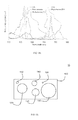
- the semiconductor quantum dot chip emission frequency peaks at a wavelength of 457 nm with emission peak Full width at half maximum (FWHM) of 25 nm.
- the wavelength up-conversion is done by using two up-conversion materials. These two wavelength up-conversion materials have individual emission peaks at 660 nm and 604 nm. These materials can be quantum dots in some embodiments.
- Figure 4 shows the combined emission peak from these two wavelength up-conversion materials peaking at 651 nm wavelength with emission peak FWHM of 101 nm. In this case about 40 % (calculated from the peak intensities) of the semiconductor quantum dot chip emission, is up-converted to 651 nm emission by two individual up-conversion materials.
- up-conversion is not used, and the longer wavelength spectral feature is emitted by at least one quantum dot that is driven by electric power.
- spectrum 40 can be used and implemented together with conventional LEDs.
- Spectrum 40 can be implemented by at least one quantum dot and at least one LED in combination in accordance with the invention.
- the spectrum 40 is especially suited to be used for illuminating at least one plant in a dark growth cavity, or a cavity with low levels of ambient light.
- embodiment 40 can be readily permuted and/or combined with any of the embodiments 10, 20, 30, 31, 50, 60, 70 and/or 80.
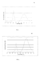
- the semiconductor quantum dot chip emission frequency peaks at a wavelength of 470 nm with emission peak Full width at half maximum (FWHM) of 30 nm.
- the wavelength up-conversion is done by using two up-conversion materials. These two wavelength up-conversion materials have individual emission peaks at 660 nm and 604 nm. These materials can be quantum dots in some embodiments.
- Figure 5 shows the combined emission peak from these two wavelength up-conversion materials peaking at 660 nm wavelength with emission peaks FWHM of 105 nm. In this case about 60 % (calculated from the peak intensities) of the semiconductor LED chip emission, is up-converted to 660 nm emission by two individual "up-conversion" materials.
- up-conversion is not used, and the longer wavelength spectral feature is emitted by at least one quantum dot that is driven by electric power.
- spectrum 50 can be used and implemented together with conventional LEDs. Spectrum 50 can also be implemented by at least one quantum dot and at least one LED in combination in accordance with the invention. The spectrum 50 is especially suited to be used for illuminating at least one plant in a dark growth cavity, or a cavity with low levels of ambient light.
- embodiment 50 can be readily permuted and/or combined with any of the embodiments 10, 20, 30, 31, 40, 50, 60, 70 and/or 80.
- the semiconductor LED chip emission frequency peaks at a wavelength of 452 nm with emission peak Full width at half maximum (FWHM) of 25 nm (not shown in the figure 6 ).
- the wavelength up-conversion is done by using one up-conversion material.
- This material can be a quantum dot in some embodiments.
- Figure 6 shows the emission peak from this up-conversion material peaking at 658 nm wavelength with emission peak FWHM of 80 nm. In this case about 100 % (calculated from the peak intensities) of the semiconductor quantum dot chip emission, is up-converted to 658 nm emission by the up-conversion material. This can be noticed from the Figure 6 , as there is no 452 nm emission exiting the quantum dot device.
- up-conversion is not used, and the longer wavelength spectral feature is emitted by at least one quantum dot that is driven by electric power.
- spectrum 60 can be used and implemented together with conventional LEDs. Spectrum 60 can be implemented also by at least one quantum dot and at least one LED in combination in accordance with the invention. The spectrum 60 is especially suited to be used for illuminating at least one plant in a dark growth cavity, or a cavity with low levels of ambient light.
- embodiment 60 can be readily permuted and/or combined with any of the embodiments 10, 20, 30, 31, 40, 50, 70 and/or 80.
- the semiconductor quantum dot chip emission frequency peaks at a wavelength of 452 nm wavelength with emission peak Full width at half maximum (FWHM) of 25 nm.
- the wavelength up-conversion is done by using one up-conversion material.
- This material can be a quantum dot in some embodiments.
- Figure 7 shows the emission peak from this up-conversion material peaking at 602 nm wavelength with emission peak FWHM of 78 nm. In this case about 95 % (calculated from the peak intensities) of the semiconductor quantum dot chip emission, is up-converted to 602 nm emission by the wavelength up-conversion material.
- up-conversion is not used, and the longer wavelength spectral feature is emitted by at least one quantum dot that is driven by electric power.
- spectrum 70 can be used and implemented together with conventional LEDs. Spectrum 70 can be implemented also by at least one quantum dot and at least one LED in combination in accordance with the invention. The spectrum 70 is especially suited to be used for illuminating at least one plant in a dark growth cavity, or a cavity with low levels of ambient light.
- embodiment 70 can be readily permuted and/or combined with any of the embodiments 10, 20, 30, 31, 40, 50, 60 and/or 80.
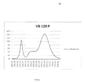
- Figure 8 shows an optimised spectrum 80 that maximises biomass production in plants.
- the optimised spectrum is preferably produced with the lighting devices of the invention described in this application.
- Spectrum 80 has special advantages in growth chamber cultivation, where the growth chamber is a dark chamber, i.e. has zero or low levels of sunlight and/or ambient light.
- the light device of the invention producing spectrum 80 can be placed into said chamber and maximise biomass production in accordance with the invention.
- the inventor has experimentally discovered the biomass maximising feature of spectrum 80.
- embodiment 80 can be readily permuted and/or combined with any of the embodiments 10, 20, 30, 31, 40, 50, 60 and/or 70.
- the used quantum dot materials and sizes should be selected in the way that a desired emission spectra from the quantum dot device is achieved.
- the present invention also concerns a lighting fixture for facilitating plant growth comprising at least one quantum dot having spectral characteristics including a peak in the wavelength range from 600 to 700 nm.
- the light sources can be designed to reach superior PPF and PPF per watt efficiency and performance and very low power consumption and very long operation lifetime when compared to the existing technologies.
- the emission at a frequency of 300-500 nm is generated by the semiconductor quantum dot chip and the emission at frequency of 400-800 nm is generated using a complete or partial wavelength up-conversion of the quantum dot chip radiation power.
- the partial wavelength up-conversion can be selected to be in range of 5-95 %, preferably 35-65 %, of the semiconductor quantum dot chip radiation.
- the wavelength up-conversion to produce the 400-800 nm radiation is achieved by using one or more up-conversion materials in proximity with the quantum dot emission source in some embodiments.
- adjustable peak wavelength as in the above is construed as a peak wavelength that can be adjusted during assembly of the lighting fixture at the factory, and/or also “adjustable” as in an adjustable dial in the lighting fixture for on site peak wavelength adjustment.
- adjusting the peak wavelengths of the quantum dots during manufacturing process of the device is also in accordance with the invention, and “adjustable” should be construed to also include adjustments made during the manufacturing process of the quantum dot. All aforementioned embodiments of an adjustable peak wavelength, or any other adjustable light source or quantum dot variable are within the scope of this patent application.
- CdSe-ZnS (core-shell) quantum dot nano particles with average particle size of 6.6nm with approximately +/- 0.5nm particle size distribution were mixed with a two component silicone encapsulant resin.
- the mixing ratio was 0.2 w-% of nano particles in the silicone resin.
- the resin containing nano particles were dispensed as encapsulant into a plastic leaded chip carrier (PLCC) consisting a InGaN light emitting diode in the PLCC cavity.
- PLCC plastic leaded chip carrier
- the light emitting diodes was determined to have electroluminescent emission at 450nm wavelength range.
- the InGaN containing PLCC package with nano particles containing encapsulant material was connect to a DC voltage power source with forward voltage of 3.2V and current of 350mA.
- the device optical emission spectrum was characterized to result in two emission peaks one at 450nm wavelength range and the second at the 660nm wavelength range.
- the 660nm wavelength range emission peak's full width at half maximum was observed to be over approximately 60nm.
- the intensity ratios of the 450nm and 660nm peaks were 0.5:1.
- the aforementioned experiment has been conducted by the applicant. It is in accordance with the invention to produce several quantum dots as described above, some of different sizes. These quantum dots, one or many quantum dots may be driven with electric current/voltage from a power source or the said one or many quantum dots may be driven by optical excitation or both optical excitation and electric current/voltage from a power source in accordance with the invention.
- the lighting system would allow a versatile control of lighting intensity and spectrum.
- the control of other abiotic parameters such as CO 2 concentration, temperature, daylight availability and humidity could be integrated within the same control system together with lighting, optimizing the crop productivity and the overall management of the greenhouse.
- the invention has been explained above with reference to the aforementioned embodiments and several commercial and industrial advantages have been demonstrated.
- the methods and arrangements of the invention allow more precise spectral tuning of the emission spectrum for lights used in plant cultivation.
- the invention therefore realises unexpected improvements in the photomorphogenetic control of plant growth, and further improvements in plant production.
- the invention also considerably improves the energy efficiency of plant cultivation relying on artificial light.
- the quality of the harvests is considerably improved with the light devices of the invention and this brings a multitude of advantages related to cultivation in dark growth chambers or chambers with very limited ambient light: Firstly plants may be grown closer to the site of consumption, e.g. in residential basements in big cities, thereby eliminating transportation costs. Secondly, plants may be grown in geographies where agriculture is not traditionally possible, e.g.
- the quality of the plants is improved also the consistency between individual plants is improved which makes harvesting easier. This is because there are less rejected individuals and machine vision based harvesting equipment can recognize the plants better when they have a consistent quality, size and colour.
- the properties of the plants may be varied in a controlled fashion because nearly all growth parameters are under control, which is especially advantageous when cultivating flowers and ornamental plants.
- a constant photon dose everyday for the plants assists in the administration of nutrients, the nutrient dose can be maintained the same year round.
- plants may be grown in dark opaque growth chambers that reflect sunlight, and are closed with lids. The energy spent in the artificial illumination of the invention is considerably less than what would have been expended in air conditioning or cooling the plant under sunlight.
Priority Applications (18)
| Application Number | Priority Date | Filing Date | Title |
|---|---|---|---|
| DE11158693T DE11158693T8 (de) | 2011-03-17 | 2011-03-17 | Pflanzenbeleuchtungsvorrichtung und Verfahren |
| EP11158693A EP2500951A1 (fr) | 2011-03-17 | 2011-03-17 | Dispositif d'éclairage horticole et procédé |
| JP2013558477A JP2014509787A (ja) | 2011-03-17 | 2012-02-08 | 植物照明装置および方法 |
| US13/695,483 US9450144B2 (en) | 2011-03-17 | 2012-02-08 | Plant illumination device and method |
| CA2827808A CA2827808C (fr) | 2011-03-17 | 2012-02-08 | Dispositif et procede d'eclairage de plantes |
| AU2012228152A AU2012228152A1 (en) | 2011-03-17 | 2012-02-08 | Plant illumination device and method |
| KR1020137026118A KR20140020953A (ko) | 2011-03-17 | 2012-02-08 | 식물 조명 장치 및 방법 |
| PCT/FI2012/050118 WO2012123627A1 (fr) | 2011-03-17 | 2012-02-08 | Dispositif et procédé d'éclairage de plantes |
| CN201280012664.9A CN103563102A (zh) | 2011-03-17 | 2012-02-08 | 植物照明装置与方法 |
| AU2012101936A AU2012101936A4 (en) | 2011-03-17 | 2012-02-08 | Plant illumination device and method |
| SG2013064985A SG192980A1 (en) | 2011-03-17 | 2012-02-08 | Plant illumination device and method |
| RU2013142884/28A RU2013142884A (ru) | 2011-03-17 | 2012-02-08 | Осветительное устройство для выращивания растений и способ освещения растений |
| TW101104867A TW201240138A (en) | 2011-03-17 | 2012-02-15 | Plant illumination device and method |
| US15/253,926 US9961841B2 (en) | 2011-03-17 | 2016-09-01 | Plant illumination device and method |
| US15/950,622 US10334789B2 (en) | 2011-03-17 | 2018-04-11 | Plant illumination device |
| US16/414,105 US10653073B2 (en) | 2011-03-17 | 2019-05-16 | Plant illumination system |
| US16/850,963 US11432472B2 (en) | 2011-03-17 | 2020-04-16 | Dark cavity lighting system |
| US17/818,146 US11864508B2 (en) | 2011-03-17 | 2022-08-08 | Dark cavity lighting system |
Applications Claiming Priority (1)
| Application Number | Priority Date | Filing Date | Title |
|---|---|---|---|
| EP11158693A EP2500951A1 (fr) | 2011-03-17 | 2011-03-17 | Dispositif d'éclairage horticole et procédé |
Publications (1)
| Publication Number | Publication Date |
|---|---|
| EP2500951A1 true EP2500951A1 (fr) | 2012-09-19 |
Family
ID=44475174
Family Applications (1)
| Application Number | Title | Priority Date | Filing Date |
|---|---|---|---|
| EP11158693A Withdrawn EP2500951A1 (fr) | 2011-03-17 | 2011-03-17 | Dispositif d'éclairage horticole et procédé |
Country Status (12)
| Country | Link |
|---|---|
| US (6) | US9450144B2 (fr) |
| EP (1) | EP2500951A1 (fr) |
| JP (1) | JP2014509787A (fr) |
| KR (1) | KR20140020953A (fr) |
| CN (1) | CN103563102A (fr) |
| AU (2) | AU2012101936A4 (fr) |
| CA (1) | CA2827808C (fr) |
| DE (1) | DE11158693T8 (fr) |
| RU (1) | RU2013142884A (fr) |
| SG (1) | SG192980A1 (fr) |
| TW (1) | TW201240138A (fr) |
| WO (1) | WO2012123627A1 (fr) |
Cited By (4)
| Publication number | Priority date | Publication date | Assignee | Title |
|---|---|---|---|---|
| WO2014066770A1 (fr) * | 2012-10-26 | 2014-05-01 | Research Triangle Institute, International | Semi-conducteurs à bande intermédiaire, hétérojonctions, et dispositifs optoélectroniques utilisant des points quantiques traités en solution, et procédés associés |
| EP2727458A1 (fr) * | 2012-11-01 | 2014-05-07 | Sharp Kabushiki Kaisha | Dispositif d'éclairage |
| CN108719446A (zh) * | 2018-04-27 | 2018-11-02 | 苏州星烁纳米科技有限公司 | 光合保鲜灯以及装置 |
| EP3892088A4 (fr) * | 2018-12-12 | 2022-01-26 | Fujian Sanan Sino-Science Photobiotech Co., Ltd. | Procédé d'éclairage pour faciliter la croissance de plantes, dispositif d'éclairage de plantes et utilisation associée |
Families Citing this family (30)
| Publication number | Priority date | Publication date | Assignee | Title |
|---|---|---|---|---|
| US8492746B2 (en) | 2011-09-12 | 2013-07-23 | SemiLEDs Optoelectronics Co., Ltd. | Light emitting diode (LED) dice having wavelength conversion layers |
| RU2640960C2 (ru) * | 2012-12-21 | 2018-01-18 | Филипс Лайтинг Холдинг Б.В. | Интерфейс для освещения в растениеводстве для взаимодействия по меньшей мере с одной системой освещения |
| US10182557B2 (en) | 2013-03-05 | 2019-01-22 | Xiant Technologies, Inc. | Photon modulation management system for stimulation of a desired response in birds |
| US9560837B1 (en) | 2013-03-05 | 2017-02-07 | Xiant Technologies, Inc. | Photon modulation management system for stimulation of a desired response in birds |
| KR102107067B1 (ko) | 2013-03-05 | 2020-05-06 | 시안트 테크놀로지스 인코포레이티드 | 포톤 변조 관리 시스템 |
| US11278009B2 (en) | 2013-03-05 | 2022-03-22 | Xiant Technologies, Inc. | Photon modulation management system for stimulation of a desired response in birds |
| US9844209B1 (en) | 2014-11-24 | 2017-12-19 | Xiant Technologies, Inc. | Photon modulation management system for stimulation of a desired response in birds |
| JP6267843B2 (ja) * | 2013-07-11 | 2018-01-24 | 交和電気産業株式会社 | 照明装置 |
| CN104934460A (zh) * | 2014-03-18 | 2015-09-23 | 联想(北京)有限公司 | 一种发光器件及其对应设备、制备方法 |
| CN105333328A (zh) * | 2014-08-08 | 2016-02-17 | 台达电子工业股份有限公司 | 植物栽种照明系统及方法 |
| US10638669B2 (en) | 2014-08-29 | 2020-05-05 | Xiant Technologies, Inc | Photon modulation management system |
| CN104966776B (zh) * | 2015-06-29 | 2018-08-31 | 广东普加福光电科技有限公司 | 一种用于led植物生长灯的长寿命量子点荧光复合薄膜及其制备方法 |
| CN105405937B (zh) * | 2015-12-15 | 2017-11-07 | 苏州东善微光光电技术有限公司 | 用于植物生长的光源及植物培养方法 |
| CN106069143A (zh) * | 2016-07-08 | 2016-11-09 | 湖南农业大学 | 一种菊花在光型植物工厂中的种植方法 |
| CN106069144A (zh) * | 2016-07-08 | 2016-11-09 | 湖南普斯赛特光电科技有限公司 | 一种在人工光型植物工厂中种植菠菜的方法 |
| CN106105811A (zh) * | 2016-07-08 | 2016-11-16 | 周智 | 一种胡萝卜在半封闭式人工光型植物工厂中的培育方法 |
| CN106171398A (zh) * | 2016-07-08 | 2016-12-07 | 湖南农业大学 | 一种藏红花室内培育开花的人工栽培方法 |
| CN106171395A (zh) * | 2016-07-08 | 2016-12-07 | 周智 | 一种利用人工光型植物工厂种植小白菜的方法 |
| CN106248882B (zh) * | 2016-08-19 | 2018-04-17 | 河北神通光电科技有限公司 | 获取植物光照led红蓝光谱比例的方法 |
| US20180135830A1 (en) * | 2016-11-15 | 2018-05-17 | Eye Lighting International Of North America, Inc. | Led grow light |
| TWI636286B (zh) * | 2017-03-31 | 2018-09-21 | 友達光電股份有限公司 | 顯示裝置 |
| US11058889B1 (en) | 2017-04-03 | 2021-07-13 | Xiant Technologies, Inc. | Method of using photon modulation for regulation of hormones in mammals |
| US10163493B2 (en) * | 2017-05-08 | 2018-12-25 | International Business Machines Corporation | SRAM margin recovery during burn-in |
| JP6500940B2 (ja) * | 2017-06-22 | 2019-04-17 | サンケン電気株式会社 | 電照菊用照明装置 |
| US10667467B2 (en) | 2018-01-24 | 2020-06-02 | Nano And Advanced Materials Institute Limited | Light control device for stimulating plant growth and method thereof |
| US11483981B1 (en) * | 2018-05-14 | 2022-11-01 | Crop One Holdings, Inc. | Systems and methods for providing a low energy use farm |
| KR102147810B1 (ko) * | 2018-07-26 | 2020-08-25 | 경북대학교 산학협력단 | 퀀텀 닷 조명을 이용한 들깻잎의 재배 방법 |
| WO2020033127A1 (fr) | 2018-08-10 | 2020-02-13 | Rosstech, Inc. | Réseau de lumières del ajustables pour l'horticulture |
| US11402089B2 (en) | 2019-06-06 | 2022-08-02 | Abundant Lighting Technology, Llc | LED growth light |
| CN114927513A (zh) * | 2022-07-21 | 2022-08-19 | 杭州华普永明光电股份有限公司 | 一种发光模组及植物照明灯具 |
Citations (4)
| Publication number | Priority date | Publication date | Assignee | Title |
|---|---|---|---|---|
| WO1999050916A1 (fr) * | 1998-04-01 | 1999-10-07 | Massachusetts Institute Of Technology | Diodes electroluminescentes de couleur et blanches a points quantiques |
| WO2009048425A1 (fr) | 2007-10-12 | 2009-04-16 | Agency For Science, Technology And Research | Fabrication de del à base de nitrure rouges et blanches sans luminophore |
| WO2010053341A1 (fr) | 2008-11-07 | 2010-05-14 | Uab "Hortiled" | Diode électroluminescente à conversion de substance fluorescente pour répondre aux besoins photomorphogénétiques des plantes |
| US20100259190A1 (en) * | 2008-09-18 | 2010-10-14 | Valoya Oy | Lighting assembly |
Family Cites Families (18)
| Publication number | Priority date | Publication date | Assignee | Title |
|---|---|---|---|---|
| US5269093A (en) * | 1990-11-30 | 1993-12-14 | Matsushita Electric Industrial Co., Ltd. | Method and apparatus for controlling plant growth with artificial light |
| US8074397B2 (en) * | 2000-02-22 | 2011-12-13 | Ccs Inc. | Illuminator for plant growth |
| US7318651B2 (en) * | 2003-12-18 | 2008-01-15 | Avago Technologies Ecbu Ip (Singapore) Pte. Ltd. | Flash module with quantum dot light conversion |
| US20070058368A1 (en) * | 2005-09-09 | 2007-03-15 | Partee Adam M | Efficient high brightness led system that generates radiometric light energy capable of controlling growth of plants from seed to full maturity |
| TWI344314B (en) * | 2005-10-14 | 2011-06-21 | Hon Hai Prec Ind Co Ltd | Light-emitting element, plane light source and direct-type backlight module |
| EP1992216B1 (fr) * | 2006-03-08 | 2018-12-05 | Shikoku Research Institute Incorporated | Procédé pour induire l'expression d'un gène résistant à une maladie d'une plante |
| WO2009014707A2 (fr) * | 2007-07-23 | 2009-01-29 | Qd Vision, Inc. | Substrat d'amélioration de lumière à point quantique et dispositif d'éclairage le comprenant |
| EP2025220A1 (fr) * | 2007-08-15 | 2009-02-18 | Lemnis Lighting Patent Holding B.V. | Lampe à DEL pour la production végétale |
| ES2342567T3 (es) * | 2007-09-28 | 2010-07-08 | Scheuten S.A.R.L. | Sistema de invernadero. |
| KR101995369B1 (ko) | 2008-04-03 | 2019-07-02 | 삼성 리서치 아메리카 인코포레이티드 | 양자점들을 포함하는 발광 소자 |
| US20090288340A1 (en) * | 2008-05-23 | 2009-11-26 | Ryan Hess | LED Grow Light Method and Apparatus |
| KR100982991B1 (ko) * | 2008-09-03 | 2010-09-17 | 삼성엘이디 주식회사 | 양자점 파장변환체, 양자점 파장변환체의 제조방법 및 양자점 파장변환체를 포함하는 발광장치 |
| WO2011016521A1 (fr) * | 2009-08-07 | 2011-02-10 | 昭和電工株式会社 | Lampe à diode à émission multicolore pour la culture de végétaux, dispositif d'éclairage et procédé de culture de végétaux |
| KR100993074B1 (ko) * | 2009-12-29 | 2010-11-08 | 엘지이노텍 주식회사 | 발광소자, 발광소자의 제조방법 및 발광소자 패키지 |
| EP2656728A1 (fr) * | 2012-04-27 | 2013-10-30 | Valoya Oy | Lumière horticole inclinable et procédé de culture de plante |
| KR102107067B1 (ko) * | 2013-03-05 | 2020-05-06 | 시안트 테크놀로지스 인코포레이티드 | 포톤 변조 관리 시스템 |
| US20140268635A1 (en) * | 2013-03-14 | 2014-09-18 | Valoya Oy | Phosphoric horticultural light |
| WO2014201329A1 (fr) * | 2013-06-14 | 2014-12-18 | Solartrack, Llc | Appareils, systèmes et procédés pour améliorer la croissance des plantes |
-
2011
- 2011-03-17 DE DE11158693T patent/DE11158693T8/de active Active
- 2011-03-17 EP EP11158693A patent/EP2500951A1/fr not_active Withdrawn
-
2012
- 2012-02-08 US US13/695,483 patent/US9450144B2/en active Active
- 2012-02-08 CN CN201280012664.9A patent/CN103563102A/zh active Pending
- 2012-02-08 AU AU2012101936A patent/AU2012101936A4/en not_active Expired
- 2012-02-08 JP JP2013558477A patent/JP2014509787A/ja active Pending
- 2012-02-08 WO PCT/FI2012/050118 patent/WO2012123627A1/fr active Application Filing
- 2012-02-08 CA CA2827808A patent/CA2827808C/fr active Active
- 2012-02-08 AU AU2012228152A patent/AU2012228152A1/en active Pending
- 2012-02-08 SG SG2013064985A patent/SG192980A1/en unknown
- 2012-02-08 KR KR1020137026118A patent/KR20140020953A/ko not_active Application Discontinuation
- 2012-02-08 RU RU2013142884/28A patent/RU2013142884A/ru not_active Application Discontinuation
- 2012-02-15 TW TW101104867A patent/TW201240138A/zh unknown
-
2016
- 2016-09-01 US US15/253,926 patent/US9961841B2/en active Active
-
2018
- 2018-04-11 US US15/950,622 patent/US10334789B2/en active Active
-
2019
- 2019-05-16 US US16/414,105 patent/US10653073B2/en active Active
-
2020
- 2020-04-16 US US16/850,963 patent/US11432472B2/en active Active
-
2022
- 2022-08-08 US US17/818,146 patent/US11864508B2/en active Active
Patent Citations (4)
| Publication number | Priority date | Publication date | Assignee | Title |
|---|---|---|---|---|
| WO1999050916A1 (fr) * | 1998-04-01 | 1999-10-07 | Massachusetts Institute Of Technology | Diodes electroluminescentes de couleur et blanches a points quantiques |
| WO2009048425A1 (fr) | 2007-10-12 | 2009-04-16 | Agency For Science, Technology And Research | Fabrication de del à base de nitrure rouges et blanches sans luminophore |
| US20100259190A1 (en) * | 2008-09-18 | 2010-10-14 | Valoya Oy | Lighting assembly |
| WO2010053341A1 (fr) | 2008-11-07 | 2010-05-14 | Uab "Hortiled" | Diode électroluminescente à conversion de substance fluorescente pour répondre aux besoins photomorphogénétiques des plantes |
Non-Patent Citations (1)
| Title |
|---|
| SOH ET AL., FABRICATION OF PHOSPHOR FREE RED AND WHITE NITRIDE-BASED LEDS, 2009 |
Cited By (5)
| Publication number | Priority date | Publication date | Assignee | Title |
|---|---|---|---|---|
| WO2014066770A1 (fr) * | 2012-10-26 | 2014-05-01 | Research Triangle Institute, International | Semi-conducteurs à bande intermédiaire, hétérojonctions, et dispositifs optoélectroniques utilisant des points quantiques traités en solution, et procédés associés |
| CN104937722A (zh) * | 2012-10-26 | 2015-09-23 | 研究三角协会 | 利用处理量子点溶液制造的中间带半导体、异质结和光电设备,及其相关方法 |
| EP2727458A1 (fr) * | 2012-11-01 | 2014-05-07 | Sharp Kabushiki Kaisha | Dispositif d'éclairage |
| CN108719446A (zh) * | 2018-04-27 | 2018-11-02 | 苏州星烁纳米科技有限公司 | 光合保鲜灯以及装置 |
| EP3892088A4 (fr) * | 2018-12-12 | 2022-01-26 | Fujian Sanan Sino-Science Photobiotech Co., Ltd. | Procédé d'éclairage pour faciliter la croissance de plantes, dispositif d'éclairage de plantes et utilisation associée |
Also Published As
| Publication number | Publication date |
|---|---|
| US20190274260A1 (en) | 2019-09-12 |
| US10653073B2 (en) | 2020-05-19 |
| US20200236863A1 (en) | 2020-07-30 |
| US9450144B2 (en) | 2016-09-20 |
| TW201240138A (en) | 2012-10-01 |
| DE11158693T8 (de) | 2013-04-25 |
| US20170006783A1 (en) | 2017-01-12 |
| US20180228093A1 (en) | 2018-08-16 |
| US20130042527A1 (en) | 2013-02-21 |
| SG192980A1 (en) | 2013-09-30 |
| RU2013142884A (ru) | 2015-04-27 |
| AU2012228152A1 (en) | 2013-09-05 |
| DE11158693T1 (de) | 2012-12-27 |
| CN103563102A (zh) | 2014-02-05 |
| KR20140020953A (ko) | 2014-02-19 |
| JP2014509787A (ja) | 2014-04-21 |
| US20220377987A1 (en) | 2022-12-01 |
| US11864508B2 (en) | 2024-01-09 |
| US9961841B2 (en) | 2018-05-08 |
| WO2012123627A1 (fr) | 2012-09-20 |
| US11432472B2 (en) | 2022-09-06 |
| US10334789B2 (en) | 2019-07-02 |
| AU2012101936A4 (en) | 2015-09-17 |
| CA2827808A1 (fr) | 2012-09-20 |
| CA2827808C (fr) | 2017-10-31 |
Similar Documents
| Publication | Publication Date | Title |
|---|---|---|
| US11864508B2 (en) | Dark cavity lighting system | |
| US9883635B2 (en) | Plant illumination device and method for dark growth chambers | |
| US9318648B2 (en) | Method and means for enhancing greenhouse lights | |
| AU2015213403B2 (en) | Plant illumination device and method for dark growth chambers |
Legal Events
| Date | Code | Title | Description |
|---|---|---|---|
| PUAI | Public reference made under article 153(3) epc to a published international application that has entered the european phase |
Free format text: ORIGINAL CODE: 0009012 |
|
| 17P | Request for examination filed |
Effective date: 20111115 |
|
| AK | Designated contracting states |
Kind code of ref document: A1 Designated state(s): AL AT BE BG CH CY CZ DE DK EE ES FI FR GB GR HR HU IE IS IT LI LT LU LV MC MK MT NL NO PL PT RO RS SE SI SK SM TR |
|
| AX | Request for extension of the european patent |
Extension state: BA ME |
|
| REG | Reference to a national code |
Ref country code: DE Ref legal event code: R082 Representative=s name: GRUND INTELLECTUAL PROPERTY GROUP PATENTANWALT, DE Ref country code: DE Ref legal event code: R082 Representative=s name: GRUND INTELLECTUAL PROPERTY GROUP, DE |
|
| REG | Reference to a national code |
Ref country code: DE Ref legal event code: R210 Effective date: 20121227 |
|
| 17Q | First examination report despatched |
Effective date: 20180827 |
|
| STAA | Information on the status of an ep patent application or granted ep patent |
Free format text: STATUS: THE APPLICATION HAS BEEN WITHDRAWN |
|
| 18W | Application withdrawn |
Effective date: 20181218 |
|
| REG | Reference to a national code |
Ref country code: HK Ref legal event code: WD Ref document number: 1172733 Country of ref document: HK |