EP2500757A1 - Method of manufacturing optical module - Google Patents
Method of manufacturing optical module Download PDFInfo
- Publication number
- EP2500757A1 EP2500757A1 EP12159734A EP12159734A EP2500757A1 EP 2500757 A1 EP2500757 A1 EP 2500757A1 EP 12159734 A EP12159734 A EP 12159734A EP 12159734 A EP12159734 A EP 12159734A EP 2500757 A1 EP2500757 A1 EP 2500757A1
- Authority
- EP
- European Patent Office
- Prior art keywords
- bonding
- load
- microbumps
- optical device
- substrate
- Prior art date
- Legal status (The legal status is an assumption and is not a legal conclusion. Google has not performed a legal analysis and makes no representation as to the accuracy of the status listed.)
- Granted
Links
Images






Classifications
-
- H—ELECTRICITY
- H10—SEMICONDUCTOR DEVICES; ELECTRIC SOLID-STATE DEVICES NOT OTHERWISE PROVIDED FOR
- H10W—GENERIC PACKAGES, INTERCONNECTIONS, CONNECTORS OR OTHER CONSTRUCTIONAL DETAILS OF DEVICES COVERED BY CLASS H10
- H10W72/00—Interconnections or connectors in packages
- H10W72/071—Connecting or disconnecting
- H10W72/073—Connecting or disconnecting of die-attach connectors
-
- H—ELECTRICITY
- H10—SEMICONDUCTOR DEVICES; ELECTRIC SOLID-STATE DEVICES NOT OTHERWISE PROVIDED FOR
- H10W—GENERIC PACKAGES, INTERCONNECTIONS, CONNECTORS OR OTHER CONSTRUCTIONAL DETAILS OF DEVICES COVERED BY CLASS H10
- H10W72/00—Interconnections or connectors in packages
- H10W72/071—Connecting or disconnecting
- H10W72/0711—Apparatus therefor
- H10W72/07183—Means for monitoring
-
- H—ELECTRICITY
- H10—SEMICONDUCTOR DEVICES; ELECTRIC SOLID-STATE DEVICES NOT OTHERWISE PROVIDED FOR
- H10W—GENERIC PACKAGES, INTERCONNECTIONS, CONNECTORS OR OTHER CONSTRUCTIONAL DETAILS OF DEVICES COVERED BY CLASS H10
- H10W72/00—Interconnections or connectors in packages
- H10W72/071—Connecting or disconnecting
- H10W72/072—Connecting or disconnecting of bump connectors
-
- H—ELECTRICITY
- H10—SEMICONDUCTOR DEVICES; ELECTRIC SOLID-STATE DEVICES NOT OTHERWISE PROVIDED FOR
- H10W—GENERIC PACKAGES, INTERCONNECTIONS, CONNECTORS OR OTHER CONSTRUCTIONAL DETAILS OF DEVICES COVERED BY CLASS H10
- H10W72/00—Interconnections or connectors in packages
- H10W72/071—Connecting or disconnecting
- H10W72/073—Connecting or disconnecting of die-attach connectors
- H10W72/07331—Connecting techniques
-
- H—ELECTRICITY
- H10—SEMICONDUCTOR DEVICES; ELECTRIC SOLID-STATE DEVICES NOT OTHERWISE PROVIDED FOR
- H10W—GENERIC PACKAGES, INTERCONNECTIONS, CONNECTORS OR OTHER CONSTRUCTIONAL DETAILS OF DEVICES COVERED BY CLASS H10
- H10W72/00—Interconnections or connectors in packages
- H10W72/071—Connecting or disconnecting
- H10W72/073—Connecting or disconnecting of die-attach connectors
- H10W72/07341—Controlling the bonding environment, e.g. atmosphere composition or temperature
-
- H—ELECTRICITY
- H10—SEMICONDUCTOR DEVICES; ELECTRIC SOLID-STATE DEVICES NOT OTHERWISE PROVIDED FOR
- H10W—GENERIC PACKAGES, INTERCONNECTIONS, CONNECTORS OR OTHER CONSTRUCTIONAL DETAILS OF DEVICES COVERED BY CLASS H10
- H10W72/00—Interconnections or connectors in packages
- H10W72/071—Connecting or disconnecting
- H10W72/073—Connecting or disconnecting of die-attach connectors
- H10W72/07351—Connecting or disconnecting of die-attach connectors characterised by changes in properties of the die-attach connectors during connecting
- H10W72/07353—Connecting or disconnecting of die-attach connectors characterised by changes in properties of the die-attach connectors during connecting changes in shapes
-
- H—ELECTRICITY
- H10—SEMICONDUCTOR DEVICES; ELECTRIC SOLID-STATE DEVICES NOT OTHERWISE PROVIDED FOR
- H10W—GENERIC PACKAGES, INTERCONNECTIONS, CONNECTORS OR OTHER CONSTRUCTIONAL DETAILS OF DEVICES COVERED BY CLASS H10
- H10W72/00—Interconnections or connectors in packages
- H10W72/20—Bump connectors, e.g. solder bumps or copper pillars; Dummy bumps; Thermal bumps
- H10W72/241—Dispositions, e.g. layouts
-
- H—ELECTRICITY
- H10—SEMICONDUCTOR DEVICES; ELECTRIC SOLID-STATE DEVICES NOT OTHERWISE PROVIDED FOR
- H10W—GENERIC PACKAGES, INTERCONNECTIONS, CONNECTORS OR OTHER CONSTRUCTIONAL DETAILS OF DEVICES COVERED BY CLASS H10
- H10W72/00—Interconnections or connectors in packages
- H10W72/30—Die-attach connectors
-
- H—ELECTRICITY
- H10—SEMICONDUCTOR DEVICES; ELECTRIC SOLID-STATE DEVICES NOT OTHERWISE PROVIDED FOR
- H10W—GENERIC PACKAGES, INTERCONNECTIONS, CONNECTORS OR OTHER CONSTRUCTIONAL DETAILS OF DEVICES COVERED BY CLASS H10
- H10W72/00—Interconnections or connectors in packages
- H10W72/30—Die-attach connectors
- H10W72/331—Shapes of die-attach connectors
- H10W72/334—Cross-sectional shape, i.e. in side view
-
- H—ELECTRICITY
- H10—SEMICONDUCTOR DEVICES; ELECTRIC SOLID-STATE DEVICES NOT OTHERWISE PROVIDED FOR
- H10W—GENERIC PACKAGES, INTERCONNECTIONS, CONNECTORS OR OTHER CONSTRUCTIONAL DETAILS OF DEVICES COVERED BY CLASS H10
- H10W72/00—Interconnections or connectors in packages
- H10W72/30—Die-attach connectors
- H10W72/351—Materials of die-attach connectors
- H10W72/352—Materials of die-attach connectors comprising metals or metalloids, e.g. solders
-
- H—ELECTRICITY
- H10—SEMICONDUCTOR DEVICES; ELECTRIC SOLID-STATE DEVICES NOT OTHERWISE PROVIDED FOR
- H10W—GENERIC PACKAGES, INTERCONNECTIONS, CONNECTORS OR OTHER CONSTRUCTIONAL DETAILS OF DEVICES COVERED BY CLASS H10
- H10W72/00—Interconnections or connectors in packages
- H10W72/30—Die-attach connectors
- H10W72/351—Materials of die-attach connectors
- H10W72/353—Materials of die-attach connectors not comprising solid metals or solid metalloids, e.g. ceramics
- H10W72/354—Materials of die-attach connectors not comprising solid metals or solid metalloids, e.g. ceramics comprising polymers
-
- H—ELECTRICITY
- H10—SEMICONDUCTOR DEVICES; ELECTRIC SOLID-STATE DEVICES NOT OTHERWISE PROVIDED FOR
- H10W—GENERIC PACKAGES, INTERCONNECTIONS, CONNECTORS OR OTHER CONSTRUCTIONAL DETAILS OF DEVICES COVERED BY CLASS H10
- H10W72/00—Interconnections or connectors in packages
- H10W72/90—Bond pads, in general
- H10W72/931—Shapes of bond pads
-
- H—ELECTRICITY
- H10—SEMICONDUCTOR DEVICES; ELECTRIC SOLID-STATE DEVICES NOT OTHERWISE PROVIDED FOR
- H10W—GENERIC PACKAGES, INTERCONNECTIONS, CONNECTORS OR OTHER CONSTRUCTIONAL DETAILS OF DEVICES COVERED BY CLASS H10
- H10W72/00—Interconnections or connectors in packages
- H10W72/90—Bond pads, in general
- H10W72/951—Materials of bond pads
- H10W72/952—Materials of bond pads comprising metals or metalloids, e.g. PbSn, Ag or Cu
-
- H—ELECTRICITY
- H10—SEMICONDUCTOR DEVICES; ELECTRIC SOLID-STATE DEVICES NOT OTHERWISE PROVIDED FOR
- H10W—GENERIC PACKAGES, INTERCONNECTIONS, CONNECTORS OR OTHER CONSTRUCTIONAL DETAILS OF DEVICES COVERED BY CLASS H10
- H10W80/00—Direct bonding of chips, wafers or substrates
- H10W80/301—Bonding techniques, e.g. hybrid bonding
- H10W80/314—Bonding techniques, e.g. hybrid bonding characterized by direct bonding of pads or other interconnections
-
- H—ELECTRICITY
- H10—SEMICONDUCTOR DEVICES; ELECTRIC SOLID-STATE DEVICES NOT OTHERWISE PROVIDED FOR
- H10W—GENERIC PACKAGES, INTERCONNECTIONS, CONNECTORS OR OTHER CONSTRUCTIONAL DETAILS OF DEVICES COVERED BY CLASS H10
- H10W90/00—Package configurations
- H10W90/701—Package configurations characterised by the relative positions of pads or connectors relative to package parts
- H10W90/731—Package configurations characterised by the relative positions of pads or connectors relative to package parts of die-attach connectors
- H10W90/734—Package configurations characterised by the relative positions of pads or connectors relative to package parts of die-attach connectors between a chip and a stacked insulating package substrate, interposer or RDL
-
- Y—GENERAL TAGGING OF NEW TECHNOLOGICAL DEVELOPMENTS; GENERAL TAGGING OF CROSS-SECTIONAL TECHNOLOGIES SPANNING OVER SEVERAL SECTIONS OF THE IPC; TECHNICAL SUBJECTS COVERED BY FORMER USPC CROSS-REFERENCE ART COLLECTIONS [XRACs] AND DIGESTS
- Y10—TECHNICAL SUBJECTS COVERED BY FORMER USPC
- Y10T—TECHNICAL SUBJECTS COVERED BY FORMER US CLASSIFICATION
- Y10T156/00—Adhesive bonding and miscellaneous chemical manufacture
- Y10T156/10—Methods of surface bonding and/or assembly therefor
- Y10T156/1002—Methods of surface bonding and/or assembly therefor with permanent bending or reshaping or surface deformation of self sustaining lamina
- Y10T156/1039—Surface deformation only of sandwich or lamina [e.g., embossed panels]
Definitions
- the present invention relates to a method of manufacturing an optical module and, more specifically, to a method of manufacturing an optical module including a plurality of optical devices bonded by using bonding bumps.
- a method of mounting a semiconductor laser element, and joining a photodiode to a copper heat sink using bonding bumps to optically align the semiconductor laser element and the photodiode with high precision is known (for example, refer to Japanese Unexamined Patent Application Publication No. H10-208269 ( FIG. 1 )).
- the relationship between pressure applied to the bonding bumps and height of the bonding bumps deformed according to the applied pressure is examined in advance, and a proper application pressure is selected according to the relationship.
- the re-deformation that the bonding bumps are deformed again to the state before the deformation after the load is released will be called “elastic return of bonding bumps", and the deformation amount will be called “elastic return amount”.
- the “elastic return amount” changes according to the amount of a load applied, the material of the bonding bumps, the shape of the bonding bumps, and the like.
- an object of the present invention is, to provide a method of manufacturing an optical module to solve the problem.
- Another object of the invention is to provide a method of manufacturing an optical module in which optical devices can be optically aligned with high precision regardless of an elastic return of bonding bumps.
- a method of manufacturing an optical module according to the present invention includes steps of forming bonding bumps made of metal on a substrate, and bonding a second optical device on the bonding bumps by applying a load so that the bonding bumps are deformed only by a predetermined amount from a position where a first optical device and the second optical device are optically coupled most efficiently and, after that, releasing the load.
- the second optical device is bonded on the bonding bumps based on the elastic return amount of the bonding bumps. Consequently, also in a state in which the load is released, the first and second optical devices can be aligned with high precision.
- FIG. 1A is a perspective view of a semiconductor laser module 1 as an example of an optical module and FIG. 1B is a side view in the Y-axis direction of the semiconductor laser module 1.
- the semiconductor laser module 1 includes a silicon substrate 10, an LD (Laser Diode) element 20, a PPLN (Periodically Poled Lithium Niobate) element 30 for converting the wavelength of light emitted from the LD element 20, a sub-substrate 40 made of silicon or glass, and an optical fiber 50.
- the semiconductor laser module 1 functions to convert single-mode laser near-infrared light having wavelength of 1,064 nm emitted from the LD element 20 to green laser light having wavelength of 532 nm in the PPLN element 30 and emit the green laser light.
- the light emitted from the PPLN element 30 is transmitted through the single-mode optical fiber (SMF) 50 bonded to the silicon substrate 10 via the sub-substrate 40.
- SMF single-mode optical fiber
- elements are optically coupled so that light emitted from the LD element 20 can efficiently enter the PPLN element 30.
- those elements are requested to be aligned at extremely high precision.
- the positional precision in the plane direction (XY plane) on the silicon substrate 10 in FIG. 1A is adjusted by a mounting device at the time of mounting by providing reference marks such as alignment marks on the silicon substrate 10.
- the mounting height is determined by contact points between the silicon substrate 10 and each of the LD element 20 and the PPLN element 30. Consequently, by forming microbumps as bonding bumps which will be described later on the silicon substrate 10 and deforming the microbumps by applying a predetermined load to the microbumps at the time of mounting the PPLN element 30, the precision in the height direction (Z direction) is maintained.
- a bonding material such as resin, AuSn, or solder can be used.
- the position adjustment can be performed by vertically moving the elements during the bonding material is in a liquid form, when the bonding material is cooled and solidified, the bonding material is shrunk and deformed unpredictably. It is consequently difficult with high-precision to adjust the position in the height direction (Z direction) .
- the semiconductor laser module 1 is an example of the optical module. It is not interpreted that the optical module is limited to the semiconductor laser module 1.
- the optical module can be preferably applied to other modules each having two or more optical devices optically coupled.
- the optical module can be used for optical coupling between the LD element 20 and the PPLN element 30 or optical coupling between the PPLN element 30 and the optical fiber 50 fixed to the sub-substrate 40.
- the optical coupling denotes that the positional relation of optical devices is determined so that light output from one of the optical devices directly enters the other optical device.
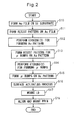
- FIG. 2 is a flowchart for explaining processes of manufacturing the semiconductor laser module 1.
- FIGS. 3A to 3D to FIGS. 5A to 5C are diagrams for more specifically explaining the processes of manufacturing the semiconductor laser module 1 illustrated in FIG. 2 .
- FIG. 3A is a cross sectional view of the silicon substrate 10.
- the entire silicon substrate 10 is heated in an oxidizing atmosphere and an SiO 2 (silicon dioxide) thin film 11 is formed on the silicon substrate 10.
- a Ti (titanium) thin film 12 is formed on the SiO 2 thin film 11 by vapor deposition.
- an Au layer 13 having a thickness of 3 ⁇ m is formed on the Ti thin film 12 by vapor deposition (S10) (refer to FIG. 3B ).
- the Au layer 13 may be formed by, in addition to vapor deposition, sputtering, electrodeposition, or the like.
- the SiO 2 thin film 11 functions as an insulating layer insulating between the silicon substrate 10 and microbumps 18 which will be described later.
- the Ti thin film 12 is formed to increase adhesion between the SiO 2 thin film 11 and the Au layer 13.
- a photoresist layer 14 is formed on the Au layer 13, a mask layer 9 is disposed, and ultraviolet light is applied so that a photoresist 14' corresponding to the mask layer 9 is formed (S11) (refer to FIG. 3C ).
- the Au layer 13 and the Ti thin film 12 out of the part in which the photoresist 14' is formed are etched by dry etching to form an Au layer pattern 13' (S12) (refer to FIG. 3D ).
- the Au layer pattern 13' may be formed by wet etching in place of dry etching.
- the photoresist layer 15 is formed again, a mask layer 16 is disposed, and ultraviolet light is applied so that a photoresist 15' corresponding to the mask layer 16 is formed (S13) (refer to FIG. 4A ).
- the Au layer pattern 13' out of the part in which the photoresist 15' is formed is half-etched by dry etching to form the microbumps 18 and microbumps 19 (S14) (refer to FIG. 4B ).
- the microbumps 18 and 19 may be formed by wet etching in place of dry etching.
- the half-etching is etching performed so that the pattern out of the part in which the photoresist 15' is formed is not entirely removed but partially remains. In the embodiment, on the outside of the part in which the photoresist 15' is formed, etching is performed so that the thickness of Au layer pattern 13' is 1 ⁇ m.
- microbumps 18 and 19 are disposed at pitches of 10 to 25 ⁇ m equally in the horizontal direction.
- the values of shape, height, width, pitch, and the like of the projection are an example and are not limited to the above-mentioned ones.
- the microbumps 18 and 19 are based on the Au layer 13 formed by sputtering (S10) and formed by half-etching (S14), so that the heights of all of the projections included in the microbumps 18 and 19 are uniformed with high precision.
- the surface is activated (S16). Since atoms having high surface energy can be made come into contact with each other by the surface activation, bonding can be firmly performed at room temperature by using adhesion between the atoms.
- This bonding method does not require special heating and occurrence of a positional deviation of each of the parts caused by residual stress of a thermal expansion coefficient difference is suppressed, so that high-precision alignment and mounting can be performed.
- the method also has advantages such that destruction of parts caused by the residual stress of a thermal expansion coefficient difference does not easily occur, no stress is applied to the parts, and very little deterioration in functions.
- the LD element 20 is mounted on the surface-activated microbumps 18 (S17) (refer to FIG. 5A ).
- An Au layer is formed also on the bonding face of the LD element 20, and its surface is subjected to activating process. Therefore, only by mounting the LD element 20 on the microbumps 18 and applying a predetermined load, the LD element 20 is surface-activated and bonded to the microbumps 18 and fixed.
- the LD element 20 can receive supply of drive current via the microbumps 18. In this case, it is sufficient to perform predetermined patterning for supplying drive current on the Au layer pattern 13' for forming the microbumps 18.
- the LD element 20 is mounted by a mounting device for attaching not-shown electronic parts on the circuit board.
- the LD element 20 may be mounted by using an aligning and mounting device 103 used in S18 to be described later.
- the PPLN element 30 is aligned and mounted on the surface-activated microbumps 19 (S18) (refer to FIG. 5B ), and the series of processes are finished.
- An Au layer is formed also on the bonding surface of the PPLN element 30, and the surface is subjected to the activating process. Therefore, only by mounting the PPLN element 30 on the microbumps 19 and applying a predetermined load, the PPLN element 30 is surface-activated and bonded on the microbumps 19 and fixed.
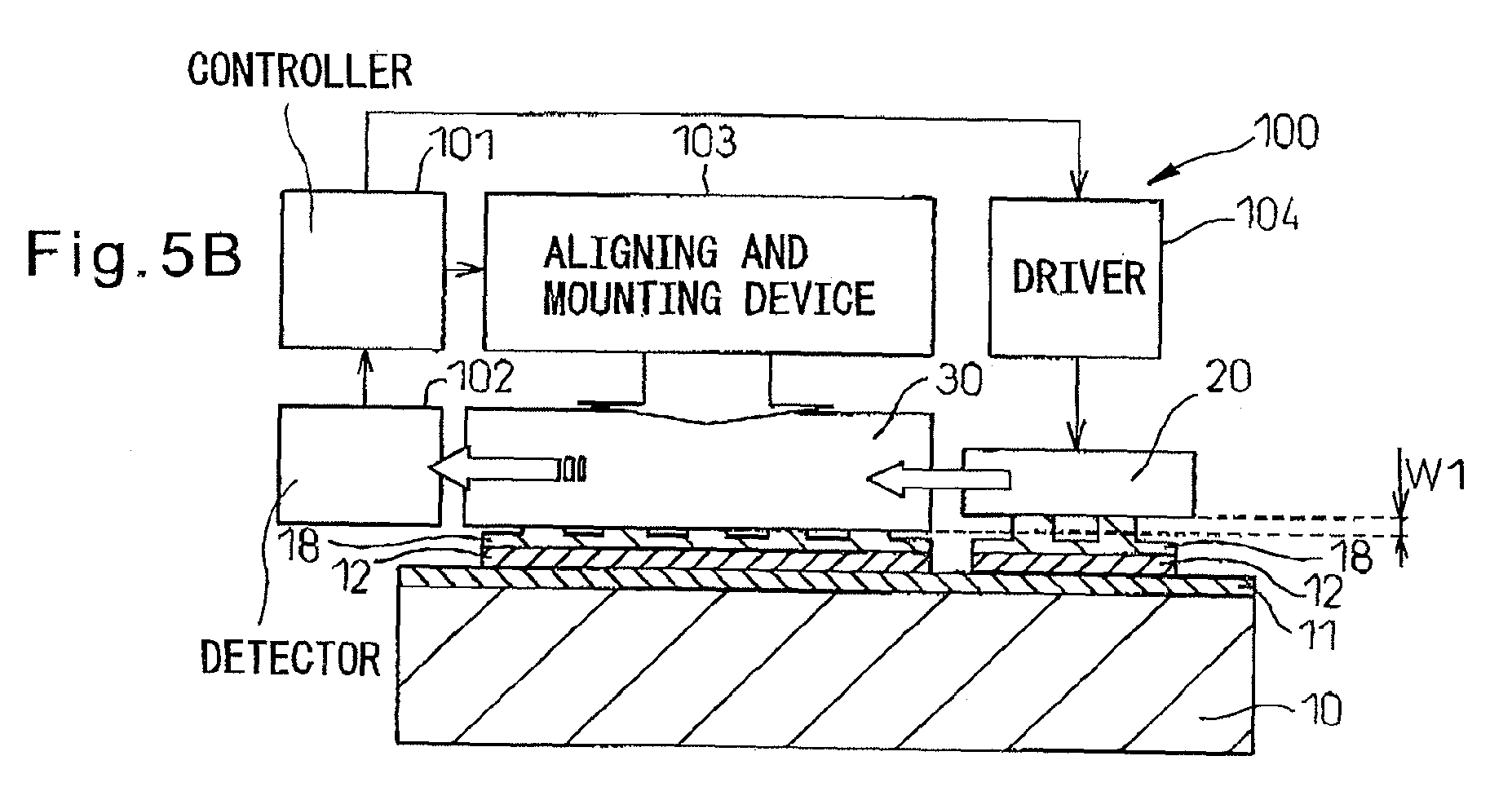
- the alignment and mounting in S18 is performed by using an aligning and mounting apparatus 100.
- the aligning and mounting apparatus 100 includes: a controller 101 constructed by, for example, a PC including a CPU, a predetermined memory, and the like; a detector 102 detecting intensity of a wavelength-converted laser beam output from the PPLN element 30 and outputting detection output voltage V (mV) according to the intensity; the aligning and mounting device 103 capable of mounting an electronic part in a predetermined position on the silicon substrate 20 and applying a load (N) according to a control amount at the time of mounting; and a driver 104 driving the LD element 20 to emit a laser beam.
- a controller 101 constructed by, for example, a PC including a CPU, a predetermined memory, and the like
- a detector 102 detecting intensity of a wavelength-converted laser beam output from the PPLN element 30 and outputting detection output voltage V (mV) according to the intensity
- the aligning and mounting device 103 capable of mounting an electronic part in a pre
- the controller 101 controls the driver 104 to drive the LD element 20 and make the laser beam enter the PPLN element 30, and the intensity of the wavelength-converted laser beam emitted from the PPLN element 30 is detected by the detector 102. Further, the controller 101 controls the aligning and mounting device 103 while monitoring output voltage V detected by the detector 102 to control the load applied to the PPLN element 30.
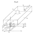
- FIG. 6 is a diagram illustrating the positional relation between the LIY element 20 and the PPLN element 30.
- a laser beam having a wavelength ⁇ 1 emitted from a light emission center 21 of the LD element 20 enters an incident position 31 in the PPLN element 30 and goes out as a laser beam having a wavelength ⁇ 2 from an outgoing center 32 of the PPLN element 30.
- the LD element 20 and the PPLN element 30 are mounted on the silicon substrate 10 by the aligning and mounting device 103, the positional relation in the plane (the positional relation in the X-Y axis direction) between the light emission center 21 of the LD element 20 and the incident position 31 in the PPLN element 30 is determined with high precision.
- the positional relation in the height direction (Z-axis direction) of the silicon substrate 10 has to be determined with high precision.
- the arrow A shows a direction in which a load is applied to the PPLN element 30 by the aligning and mounting device 103.
- FIG. 7 is a graph showing the relation between output voltage of the detector 102 and a load applied by the aligning and mounting device 103.
- the curve B indicates the relation between output voltage (mV) of the detector 102 and the load (N) applied by the aligning and mounting device 103 in a state where the load is applied.
- the curve C indicates the relationship between the output voltage (mV) of the detector 102 and the final load (N) applied by the aligning and mounting device 103 after the load is released.
- the output voltage (mV) of the detector 102 in the state where the load is applied, in the case where the load is 400 (N), the output voltage (mV) of the detector 102 becomes the maximum value (refer to point D).
- the output voltage (mV) of the detector 102 does not become the maximum value (refer to point E).
- the point D corresponds to the case where the microbumps 19 are deformed by applying a load to the PPLN element 30 to set the incident position 31 of the PPLN element 30 to a position (refer to the position P2 in FIG. 6 ) in which the incident position 31 is most-efficiently optically coupled to the light emission center 21 of the LD element 20 and, in this state, the load is released.
- the microbumps 19 have a characteristic such that when the load is applied, the microbumps 19 are deformed (pressed) and shrunk. When the load is released by elastic rebound, the force of returning to the original state works, and the microbumps 19 return to the original state only by the elastic return amount. That is, the point E corresponds to the case where when the load is released in the state of the point D, the incident position 31 of the PPLN element 30 moves to another position (for example, refer to the position P1 in FIG. 6 ) by the elastic return.
- the incident position 31 of the PPLN element 30 has to be set to the position (refer to the position P2 in FIG. 6 ) in which the incident position 31 is most-efficiently and optically coupled to the light emission center 21 of the LD element 20. Consequently, in the aligning and mounting in S18, the controller 101 controls the aligning and mounting device 103 as follows.
- the PPLN element 30 is disposed in the predetermined position of the microbumps 19. While increasing the load applied, after the output voltage V from the detector 102 becomes the maximum value, a predetermined load amount is applied to further deform the microbumps 19 and, then, the load is released.
- the controller 101 further applies a predetermined load amount (F: 200(N)) and, after that, the load is released.
- the predetermined load F is further applied so that the incident position 31 of the PPLN element 30 is pushed into a position (refer to the position P3 in FIG. 6 ) deeply pushed from the light emission center 21 of the LD element 20 only by the distance W1 shown in FIG. 6 .
- the incident position 31 of the PPLN element 30 returns to the position where it is most-efficiently optically coupled to the light emission center 21 of the LD element 20 (refer to P2 in FIG. 6 ) by elastic return (refer to FIG. 5C ).
- the above-described predetermined load amount (F: 200(N)) varies depending on the shape of the aligning and mounting device 103 and the PPLN element 30 to which the load is applied, the material and the shape of the microbumps 19, and the like- It can be calculated by conducting an experiment to obtain the curves B and C shown in FIG. 7 .
- the controller 101 controls the aligning and mounting device 103 so as to apply a predetermined load.
- the user may control the aligning and mounting device 103 while observing the output voltage V from the detector 102 by a monitor.
- FIG. 8 is a diagram showing another example of the process of manufacturing the semiconductor laser module 1.
- the controller 101 controls the aligning and mounting device 103 so as to apply a predetermined load.
- the controller 101 controls the aligning and mounting device 103 so as to apply a predetermined load.
- the microbumps 18 and 19 the LD element 20, and the PPLN element 30 manufactured with a predetermined reference, it is not always necessary to make the LD element 20 emit light and individually perform the aligning and mounting according to the output voltage V from the detector 102.
- the load at which the output voltage V from the detector 102 becomes the maximum value (refer to the point D in FIG. 7 ) is predicted and, in addition to the load (for example, 400 (N)), the above-described predetermined load amount (F: 200(N)) is applied (for example, 600 (N) in total).
- the incident position 31 of the PPLN element 30 is pushed into the position (refer to the position P3 in FIG. 6 ) which is further deeply pushed from the light emission center 21 of the LD element 20 only by the distance W1 shown in FIG. 6 and, after that, the load is released.
- the incident position 31 of the PPLN element 30 returns to the position where it is most-efficiently optically coupled to the light emission center 21 of the LD element 20 (refer to P2 in FIG. 6 ) by elastic return. That is, in the example of FIG. 8 , using only the aligning and mounting device 103, without using the controller 101, the detector 102, and the driver 104 shown in FIG. 5B , the positional relation in the height direction (Z-axis direction) between the PPLN element 30 and the LD element 20 is set.
- the method shown in FIG. 8 is different from the manufacturing process of the semiconductor laser module 1 illustrated in FIG. 2 only with respect to the point that only the aligning and mounting device 103 is used and the controller 101, the detector 102, and the driver 104 are not used in the aligning and mounting process (S18 in FIG. 2 ). Since the other points, particularly, the process of manufacturing the microbumps 18 and 19 and the method of bonding the LD element 20 and the PPLN element 30 and the microbumps 18 and 19 are the same, their description will not be repeated.
- FIGS. 9A to 9C are diagrams for explaining other microbumps.
- the microbumps 18 and 19 shown in FIGS. 4 and 5 include a plurality of projections each having a columnar shape and having a height of 2 ⁇ m and a diameter of 5 ⁇ m, which are disposed at pitches of 10 to 25 ⁇ m equally in the horizontal direction.
- Other microbumps 18' and 19' shown in FIG. 9A include a plurality of projections each having a truncated cone shape.
- FIG. 9A is a cross section of the microbumps 18' and 19' and others, and corresponds to FIG. 4C .
- FIG. 9B is a cross section of a projection part 60 included in the microbumps 18' and 19'
- FIG. 9C is a diagram showing an example of a pressed projection part 61 included in the microbumps 18' and 19'.
- the bottom face has a circular shape having a diameter S1 (for example, 2 ⁇ m)
- the top face has a circular shape having a diameter S2 (for example, 1 ⁇ m)
- height is T1 (for example, 2 ⁇ m).
- the microbumps 18' and 19' include the projection parts 60 which are disposed at pitches of 2 ⁇ m and equally in the horizontal direction.
- FIG. 9C shows an example of the projection part 61 which is pressed at the time of aligning and mounting the PPLN element 30.
- the bottom face has a circular shape having a diameter S1 (for example, 2 ⁇ m), and height is T2 (for example, 1 ⁇ m).
- S1 for example, 2 ⁇ m
- T2 for example, 1 ⁇ m
- microbumps 18' and 19' each having the truncated cone shape of which top face is slightly smaller are pressed more easily as compared with the microbumps 18 and 19 each having a columnar shape shown in FIGS. 4B and 4C and FIGS. 5A to 5C in the case of applying the same load. There is consequently an effect that the control for alignment is easier (for the reason that the aligning and mounting device 103 does not have to apply a high load).
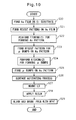
- FIG. 10 is a flowchart for explaining processes of the semiconductor laser module 2.
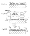
- FIGS. 11A to 11C are diagrams for explaining processes of manufacturing the semiconductor laser module 2 shown in FIG. 10 more specifically.
- the difference between the semiconductor laser module 2 and the foregoing semiconductor laser module 1 is the point that, in the semiconductor laser module 2, the PPLN element 30 and the microbumps 19 are fixed by a thermosetting bonding resin. Therefore, the Au layer is not formed on the substrate on the microbumps side of the PPLN element 30. Since it is unnecessary to supply current to the PPLN element 30 in the semiconductor laser module 2, the PPLN element 30 is fixed on the microbumps 19 by a thermosetting bonding resin without using a high-cost Au layer. Except for this point, the semiconductor laser module 2 is similar to the semiconductor laser module 1. Accordingly, S20 to S25 and S27 in the processes of manufacturing the semiconductor laser module 2 shown in FIG. 10 are the same as S10 to S15 and S17 in the processes of manufacturing the semiconductor laser module 1 shown in FIG. 2 , and their description will not be repeated.
- the surface activation is performed by performing cleaning and/or a treatment using plasma only on the surface of the microbumps 18 in S26.
- the surface activating process may be performed also on the microbumps 19.
- the LD element 20 is mounted in S27 like in S17 in FIG. 2 and, after that, a resin 70 for bonding is applied on the microbumps 19 (refer to FIG. 11A ).
- a resin 70 for bonding a thermosetting resin, a UV curable resin, or the like for optical parts can be used.
- the PPLN element 30 is aligned and mounted with heat on the resin 70 for bonding (S29) (refer to FIG. 11B ).
- the aligning and mounting method in S29 is the same as that in S18 in FIG. 2 and in FIG. 5B . Therefore, the controller 101 preliminarily considers the elastic return amount of the microbumps 19 and, after the output voltage V from the detector 102 becomes the maximum value (refer to the point D), further applies a predetermined load amount (F: 200(N)) to the PPLN element 30.
- the controller 101 further applies a predetermined load so that the incident position 31 of the PPLN element 30 is pushed in to a position which is further deeply pressed from the light emission center 21 of the LD element 20 only by the distance W3 shown in FIG. 11B .
- heating is performed to harden the resin 70 for bonding in a state where the load is further applied.
- the incident position 31 of the PPLN element 30 returns to the position where it most-efficiently optically couples to the light emission center 21 of the LD element 20 by elastic return (refer to FIG. 11C ). After that, the series of processes are finished.
- the LD element 20 and the silicon substrate 10 may be bonded by using the resin 70 for bonding.
- the resin 70 for bonding In the case where it is necessary to make the LD element 20 and the silicon substrate 10 conducted via the microbumps 18, it is sufficient to make the resin 70 for bonding penetrate the microbumps 18. Further, in the case where it is necessary to make the LD element 20 and the silicon substrate 10 conducted by an adhesive, it is sufficient to bond the LD element 20 and the silicon substrate 10 by using a conductive adhesive.
- the aligning and mounting device 103 may be used without using the controller 101, the detector 102, and the driver 104.
- FIG. 12 is a diagram for explaining bonding between the substrate 10 and the sub-substrate 40.
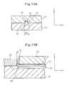
- FIGS. 13A and 13B are diagrams illustrating the positional relationship between the PPLN element 30 and the fiber 50.
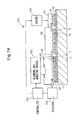
- FIG. 14 is a diagram for explaining aligning and mounting of the sub-substrate 40.
- a rectangular groove 51 is formed in the sub-substrate 40, and a front-end part 58 of the optical fiber 50 is fit in the rectangular groove 51 and fixed by an adhesive 57. It is also possible to form a V-shaped groove in place of the rectangular groove 51 in the sub-substrate 40 and fit and fix the front-end part 58 of the optical fiber 50 in the V-shaped groove.
- Metal thin films 54 and alignment marks 56 are provided in a bonding face of the sub-substrate 40.
- a fiber escape groove 52, microbumps 53, and alignment marks 55 are provided.
- the sub-substrate 40 is mounted on the silicon substrate 10 by the aligning and mounting device 103 as will be described later.
- positions are roughly determined by the alignment marks 55 and alignment marks 56.
- the positions in the X-axis direction, Y-axis direction, and Z-axis direction are determined in the submicron order, and the sub-substrate 40 is bonded on the silicon substrate 10.
- the microbumps 53 formed on the joint face of the sub-substrate 40 and the silicon substrate 10 are subjected to the plasma cleaning process so that the surface is activated and, after that, bonded by a load applied from the aligning and mounting device 103.
- the microbumps 53 made of gold formed on the silicon substrate 10 are formed on the silicon substrate 10 by a method similar to the above-described method of forming the microbumps 18 and 19.
- FIG. 13A is a cross section taken along line B-B' in FIG. 1A .
- the optical fiber 50 fixed in the rectangular groove 51 in the sub-substrate 40 by an adhesive 57 can move in the fiber escape groove 52 provided in the silicon substrate 10 by moving sub-substrate 40 in the X-axis and Y-axis directions by the aligning and mounting device 103. That is, the position adjustment in the X-axis and Y-axis directions can be performed within the range of the width W4 of the fiber escape groove 52.
- the microbumps 53 and the like are not shown.
- FIG. 13B is a cross section taken along line C-C' in FIG. 1A .
- the front-end part 58 of the optical fiber 50 fixed in the sub-substrate 40 is optically coupled to the outgoing center 32 of the PPLN element 30 with high precision and receives a wavelength-converted green laser beam having a wavelength of 532 nm which is output from the outgoing center 32 of the PPLN element 30.
- the green laser beam having a wavelength of 532 nm received by the front-end part 58 of the optical fiber 50 propagates through the optical fiber 50.
- the microbumps 53 and so one are not shown in FIG. 13B , the alignment of the outgoing center 32 of the PPLN element and the front-end part 58 of the optical fiber 50 in the Z direction is controlled by the microbumps 53.
- FIG. 14 aligning and mounting of the sub-substrate 40 will be described.
- the example of FIG. 5B (S18 in FIG. 2 ) relates to the aligning and mounting of the PPLN element 30.
- the sub-substrate 40 is aligned and mounted so that the outgoing center 32 of the PPLN element 30 and the front-end part 58 of the optical fiber 50 are optically coupled with high precision. It is assumed that, prior to the aligning and mounting of FIG. 14 , the surface of the metal thin film 54 on the joint face side of the sub-substrate 40 and the microbumps 53 on the silicon substrate 10 are subjected to the plasma cleaning process.
- the aligning and mounting in FIG. 14 is performed by using the aligning and mounting device 100 in a manner similar to the case of FIG. 5B .
- the controller 101 controls the driver 104 to drive the LD element 20 and make the laser beam enter the PPLN element 30, and the intensity of a laser beam emitted from the PPLN element 30 and transmitted through the optical fiber 50 is detected by the detector 102.
- the controller 101 controls the aligning and mounting device 103 while monitoring the output voltage v detected by the detector 102 and, while moving the sub-substrate 40 in the X-axis and Y-axis directions, determines the position where the output voltage V is the highest (first stage).
- the aligning and mounting device 103 moves the sub-substrate 40 in the X-axis and Y-axis directions in this range.
- the controller 101 controls the aligning and mounting device 103 and disposes the sub-substrate 40 on the microbumps 53 in the position where the output voltage V is the highest in the first stage.
- the controller 101 While monitoring the output voltage V detected by the detector 102, the controller 101 controls the aligning and mounting device 103 to control the load applied to the sub-substrate 40 and to position the sub-substrate 40 in the Z-axis direction (second stage). After the output voltage V from the detector 102 becomes the maximum value, the controller 101 further applies a predetermined load amount and, then, releases the load. A predetermined load is further applied so that the front-end part 58 of the optical fiber 50 fixed in the sub-substrate 40 is in the position which is further deeply pressed from the outgoing center 32 of the PPLN element 30 only by predetermined distance.
- the front-end part 58 of the optical fiber 50 fixed to the sub-substrate 40 returns to the position where it is optically coupled to the outgoing center 32 of the PPLN element 30 most efficiently by elastic return.
- the above point is based on the theory similar to the aligning and mounting for optically coupling the PLLN element 30 and the LD element 20 described with reference to FIGS. 5A to 5C to FIG. 7 .
- the sub-substrate 40 is positioned in the X-axis and Y-axis directions in the first stage and is positioned in the Z-axis direction in the second stage.
- the sub-substrate 40 may be bonded to the silicon substrate 10 by using microbumps similar to the different microbumps 18' and 19' shown in FIG. 9 .
- the sub-substrate 40 may be bonded to the silicon substrate 10 by using an adhesive.
- the microbumps 18, 19, and 53 each having a cylindrical projection and made of Au (refer to FIG. 4C ) and the microbumps 18' and 19' each having a truncated cone shape and made of Au (refer to FIG. 9 ) have been described.
- Other bonding bumps may be used as long as they are made of metal and have a shape formed with high precision.
- the conditions requested for the bonding bumps are that bumps have a material and a shape by which a deformation amount in the case of applying a predetermined load and an elastic return amount in the case of releasing a predetermined load which is applied are always almost constant.
- the sub-substrate 40 to which the LD element 20, the PPLN element 30, and the optical fiber 50 are fixed is bonded to the silicon substrate 10 by surface-activation bonding using the microbumps.
- the sub-substrate 40 to which only the LD element 20 and the PPLN element 30 or the PPLN element 30 and the optical fiber 50 are fixed may be bonded to the silicon substrate 10 by surface-activation bonding using the microbumps so that optical coupling is carried out excellently.
Landscapes
- Optical Couplings Of Light Guides (AREA)
- Semiconductor Lasers (AREA)
- Optical Modulation, Optical Deflection, Nonlinear Optics, Optical Demodulation, Optical Logic Elements (AREA)
Abstract

Description
- The entire content of Japanese Patent Application No.
2011-060916 - The present invention relates to a method of manufacturing an optical module and, more specifically, to a method of manufacturing an optical module including a plurality of optical devices bonded by using bonding bumps.
- A method of mounting a semiconductor laser element, and joining a photodiode to a copper heat sink using bonding bumps to optically align the semiconductor laser element and the photodiode with high precision is known (for example, refer to Japanese Unexamined Patent Application Publication No.
H10-208269 FIG. 1 )). - In the method, in the case of joining the photodiode with the bonding bumps, the relationship between pressure applied to the bonding bumps and height of the bonding bumps deformed according to the applied pressure is examined in advance, and a proper application pressure is selected according to the relationship.
- There is however no technique of positioning in the height direction of an optical device in submicron order by pressing bonding bumps.
- When a load is applied to the bonding bumps to deform the bonding bumps and, after that, is released, a force of returning from the deformed position to the original position acts on the deformed bonding bumps by elasticity of the bonding bumps. Even if the optical devices are aligned in a state where the load is applied to the bonding bumps, when the load is released (the applied load is removed), the bonding bumps are deformed again to return to the original state. The relative positions of the optical devices change which is inconvenient.
- The re-deformation that the bonding bumps are deformed again to the state before the deformation after the load is released will be called "elastic return of bonding bumps", and the deformation amount will be called "elastic return amount". The "elastic return amount" changes according to the amount of a load applied, the material of the bonding bumps, the shape of the bonding bumps, and the like.
- Therefore, an object of the present invention is, to provide a method of manufacturing an optical module to solve the problem.
Another object of the invention is to provide a method of manufacturing an optical module in which optical devices can be optically aligned with high precision regardless of an elastic return of bonding bumps. - A method of manufacturing an optical module according to the present invention includes steps of forming bonding bumps made of metal on a substrate, and bonding a second optical device on the bonding bumps by applying a load so that the bonding bumps are deformed only by a predetermined amount from a position where a first optical device and the second optical device are optically coupled most efficiently and, after that, releasing the load.
- According to the present invention, the second optical device is bonded on the bonding bumps based on the elastic return amount of the bonding bumps. Consequently, also in a state in which the load is released, the first and second optical devices can be aligned with high precision.
-
-
FIGS. 1A and 1B are diagrams illustrating asemiconductor laser module 1. -
FIG. 2 is a flowchart for explaining processes of manufacturing thesemiconductor laser module 1. -
FIGS. 3A, 3B, 3C and 3D are diagrams (1) illustrating processes of manufacturing thesemiconductor laser module 1. -
FIGS. 4A, 4B and 4C are diagrams (2) illustrating processes of manufacturing thesemiconductor laser module 1. -
FIGS. 5A, 5B and 5C are diagrams (3) illustrating processes of manufacturing thesemiconductor laser module 1. -
FIG. 6 is a diagram illustrating the positional relation between anLD element 20 and aPPLN element 30. -
FIG. 7 is a graph showing the relation between output voltage of adetector 102 and a load applied by an aligning andmounting device 103. -
FIG. 8 is a diagram showing another example of the process of manufacturing thesemiconductor laser module 1. -
FIGS. 9A, 9B and 9C are diagrams for explaining other microbumps. -
FIG. 10 is a flowchart for explaining processes of anothersemiconductor laser module 2. -
FIGS. 11A, 11B and 11C are diagrams illustrating processes of manufacturing the anothersemiconductor laser module 2. -
FIG. 12 is a diagram for explaining bonding between asubstrate 10 and asub-substrate 40. -
FIGS. 13A and 13B are diagrams illustrating the positional relationship between thePPLN element 30 and afiber 50. -
FIG. 14 is a diagram (4) illustrating the process of manufacturing thesemiconductor laser module 1. - Hereinafter, with reference to the drawings, a method of manufacturing an optical module according to the present disclosure will be described. It should be noted that the technical scope of the present invention is not limited to embodiments of the invention but covers the invention described in the claims and its equivalent.
-
FIG. 1A is a perspective view of asemiconductor laser module 1 as an example of an optical module andFIG. 1B is a side view in the Y-axis direction of thesemiconductor laser module 1. - The
semiconductor laser module 1 includes asilicon substrate 10, an LD (Laser Diode)element 20, a PPLN (Periodically Poled Lithium Niobate)element 30 for converting the wavelength of light emitted from theLD element 20, asub-substrate 40 made of silicon or glass, and anoptical fiber 50. For example, thesemiconductor laser module 1 functions to convert single-mode laser near-infrared light having wavelength of 1,064 nm emitted from theLD element 20 to green laser light having wavelength of 532 nm in thePPLN element 30 and emit the green laser light. The light emitted from thePPLN element 30 is transmitted through the single-mode optical fiber (SMF) 50 bonded to thesilicon substrate 10 via thesub-substrate 40. - In the
semiconductor laser module 1, elements are optically coupled so that light emitted from theLD element 20 can efficiently enter thePPLN element 30. To increase the optical coupling efficiency, those elements are requested to be aligned at extremely high precision. The positional precision in the plane direction (XY plane) on thesilicon substrate 10 inFIG. 1A is adjusted by a mounting device at the time of mounting by providing reference marks such as alignment marks on thesilicon substrate 10. - However, normally, with respect to the precision in the height direction (Z direction) in
FIG. 1A , without taking any measure, the mounting height is determined by contact points between thesilicon substrate 10 and each of theLD element 20 and thePPLN element 30. Consequently, by forming microbumps as bonding bumps which will be described later on thesilicon substrate 10 and deforming the microbumps by applying a predetermined load to the microbumps at the time of mounting thePPLN element 30, the precision in the height direction (Z direction) is maintained. - In the case of mounting the
LD element 20 and thePPLN element 30 on thesilicon substrate 10, a bonding material such as resin, AuSn, or solder can be used. Although the position adjustment can be performed by vertically moving the elements during the bonding material is in a liquid form, when the bonding material is cooled and solidified, the bonding material is shrunk and deformed unpredictably. It is consequently difficult with high-precision to adjust the position in the height direction (Z direction) . - The
semiconductor laser module 1 is an example of the optical module. It is not interpreted that the optical module is limited to thesemiconductor laser module 1. The optical module can be preferably applied to other modules each having two or more optical devices optically coupled. For example, as will be described later, the optical module can be used for optical coupling between theLD element 20 and thePPLN element 30 or optical coupling between thePPLN element 30 and theoptical fiber 50 fixed to thesub-substrate 40. The optical coupling denotes that the positional relation of optical devices is determined so that light output from one of the optical devices directly enters the other optical device. - With reference to
FIG. 2 to FIG. 5C , a part regarding bonding of theLD element 20 and thePLLN element 30, in processes of manufacturing thesemiconductor laser module 1 as an example of the optical module will be described.FIG. 2 is a flowchart for explaining processes of manufacturing thesemiconductor laser module 1.FIGS. 3A to 3D toFIGS. 5A to 5C are diagrams for more specifically explaining the processes of manufacturing thesemiconductor laser module 1 illustrated inFIG. 2 . - First, the
silicon substrate 10 is prepared.FIG. 3A is a cross sectional view of thesilicon substrate 10. - Next, the
entire silicon substrate 10 is heated in an oxidizing atmosphere and an SiO2 (silicon dioxide)thin film 11 is formed on thesilicon substrate 10. A Ti (titanium)thin film 12 is formed on the SiO2thin film 11 by vapor deposition. Further, anAu layer 13 having a thickness of 3 µm is formed on the Tithin film 12 by vapor deposition (S10) (refer toFIG. 3B ). TheAu layer 13 may be formed by, in addition to vapor deposition, sputtering, electrodeposition, or the like. The SiO2thin film 11 functions as an insulating layer insulating between thesilicon substrate 10 andmicrobumps 18 which will be described later. The Tithin film 12 is formed to increase adhesion between the SiO2thin film 11 and theAu layer 13. - Subsequently, a
photoresist layer 14 is formed on theAu layer 13, a mask layer 9 is disposed, and ultraviolet light is applied so that a photoresist 14' corresponding to the mask layer 9 is formed (S11) (refer toFIG. 3C ). - The
Au layer 13 and the Tithin film 12 out of the part in which the photoresist 14' is formed are etched by dry etching to form an Au layer pattern 13' (S12) (refer toFIG. 3D ). The Au layer pattern 13' may be formed by wet etching in place of dry etching. - After removing the photoresist 14', the
photoresist layer 15 is formed again, amask layer 16 is disposed, and ultraviolet light is applied so that a photoresist 15' corresponding to themask layer 16 is formed (S13) (refer toFIG. 4A ). - The Au layer pattern 13' out of the part in which the photoresist 15' is formed is half-etched by dry etching to form the
microbumps 18 and microbumps 19 (S14) (refer toFIG. 4B ). Themicrobumps - Subsequently, the photoresist 15' is removed, and formation of the
microbumps FIG. 4C ). Themicrobumps microbumps Au layer 13 formed by sputtering (S10) and formed by half-etching (S14), so that the heights of all of the projections included in themicrobumps - By plasma-cleaning an oxide film or an inactive layer such as contamination covering the surface of the
microbumps - Next, the
LD element 20 is mounted on the surface-activated microbumps 18 (S17) (refer toFIG. 5A ). An Au layer is formed also on the bonding face of theLD element 20, and its surface is subjected to activating process. Therefore, only by mounting theLD element 20 on themicrobumps 18 and applying a predetermined load, theLD element 20 is surface-activated and bonded to themicrobumps 18 and fixed. TheLD element 20 can receive supply of drive current via themicrobumps 18. In this case, it is sufficient to perform predetermined patterning for supplying drive current on the Au layer pattern 13' for forming themicrobumps 18. - The
LD element 20 is mounted by a mounting device for attaching not-shown electronic parts on the circuit board. TheLD element 20 may be mounted by using an aligning and mountingdevice 103 used in S18 to be described later. - The
PPLN element 30 is aligned and mounted on the surface-activated microbumps 19 (S18) (refer toFIG. 5B ), and the series of processes are finished. An Au layer is formed also on the bonding surface of thePPLN element 30, and the surface is subjected to the activating process. Therefore, only by mounting thePPLN element 30 on themicrobumps 19 and applying a predetermined load, thePPLN element 30 is surface-activated and bonded on themicrobumps 19 and fixed. - The alignment and mounting in S18 is performed by using an aligning and mounting
apparatus 100. The aligning and mountingapparatus 100 includes: acontroller 101 constructed by, for example, a PC including a CPU, a predetermined memory, and the like; adetector 102 detecting intensity of a wavelength-converted laser beam output from thePPLN element 30 and outputting detection output voltage V (mV) according to the intensity; the aligning and mountingdevice 103 capable of mounting an electronic part in a predetermined position on thesilicon substrate 20 and applying a load (N) according to a control amount at the time of mounting; and adriver 104 driving theLD element 20 to emit a laser beam. - The
controller 101 controls thedriver 104 to drive theLD element 20 and make the laser beam enter thePPLN element 30, and the intensity of the wavelength-converted laser beam emitted from thePPLN element 30 is detected by thedetector 102. Further, thecontroller 101 controls the aligning and mountingdevice 103 while monitoring output voltage V detected by thedetector 102 to control the load applied to thePPLN element 30. -
FIG. 6 is a diagram illustrating the positional relation between theLIY element 20 and thePPLN element 30. - A laser beam having a wavelength λ1 emitted from a
light emission center 21 of theLD element 20 enters anincident position 31 in thePPLN element 30 and goes out as a laser beam having a wavelength λ2 from anoutgoing center 32 of thePPLN element 30. As shown inFIG. 6 , theLD element 20 and thePPLN element 30 are mounted on thesilicon substrate 10 by the aligning and mountingdevice 103, the positional relation in the plane (the positional relation in the X-Y axis direction) between thelight emission center 21 of theLD element 20 and theincident position 31 in thePPLN element 30 is determined with high precision. However, the positional relation in the height direction (Z-axis direction) of thesilicon substrate 10 has to be determined with high precision. InFIG. 6 , the arrow A shows a direction in which a load is applied to thePPLN element 30 by the aligning and mountingdevice 103. -
FIG. 7 is a graph showing the relation between output voltage of thedetector 102 and a load applied by the aligning and mountingdevice 103. - In
FIG. 7 , the curve B indicates the relation between output voltage (mV) of thedetector 102 and the load (N) applied by the aligning and mountingdevice 103 in a state where the load is applied. The curve C indicates the relationship between the output voltage (mV) of thedetector 102 and the final load (N) applied by the aligning and mountingdevice 103 after the load is released. In the example ofFIG. 7 , in the state where the load is applied, in the case where the load is 400 (N), the output voltage (mV) of thedetector 102 becomes the maximum value (refer to point D). However, after the load is released, in the case where the final load is 400 (N), the output voltage (mV) of thedetector 102 does not become the maximum value (refer to point E). - The point D corresponds to the case where the
microbumps 19 are deformed by applying a load to thePPLN element 30 to set theincident position 31 of thePPLN element 30 to a position (refer to the position P2 inFIG. 6 ) in which theincident position 31 is most-efficiently optically coupled to thelight emission center 21 of theLD element 20 and, in this state, the load is released. Themicrobumps 19 have a characteristic such that when the load is applied, themicrobumps 19 are deformed (pressed) and shrunk. When the load is released by elastic rebound, the force of returning to the original state works, and themicrobumps 19 return to the original state only by the elastic return amount. That is, the point E corresponds to the case where when the load is released in the state of the point D, theincident position 31 of thePPLN element 30 moves to another position (for example, refer to the position P1 inFIG. 6 ) by the elastic return. - In the state where the load is released (state where the
semiconductor laser module 1 is actually used), theincident position 31 of thePPLN element 30 has to be set to the position (refer to the position P2 inFIG. 6 ) in which theincident position 31 is most-efficiently and optically coupled to thelight emission center 21 of theLD element 20. Consequently, in the aligning and mounting in S18, thecontroller 101 controls the aligning and mountingdevice 103 as follows. ThePPLN element 30 is disposed in the predetermined position of themicrobumps 19. While increasing the load applied, after the output voltage V from thedetector 102 becomes the maximum value, a predetermined load amount is applied to further deform themicrobumps 19 and, then, the load is released. - Specifically, after the output voltage V from the
detector 102 becomes the maximum value (refer to the point D), thecontroller 101 further applies a predetermined load amount (F: 200(N)) and, after that, the load is released. The predetermined load F is further applied so that theincident position 31 of thePPLN element 30 is pushed into a position (refer to the position P3 inFIG. 6 ) deeply pushed from thelight emission center 21 of theLD element 20 only by the distance W1 shown inFIG. 6 . After that, by releasing the load, theincident position 31 of thePPLN element 30 returns to the position where it is most-efficiently optically coupled to thelight emission center 21 of the LD element 20 (refer to P2 inFIG. 6 ) by elastic return (refer toFIG. 5C ). - The above-described predetermined load amount (F: 200(N)) varies depending on the shape of the aligning and mounting
device 103 and thePPLN element 30 to which the load is applied, the material and the shape of themicrobumps 19, and the like- It can be calculated by conducting an experiment to obtain the curves B and C shown inFIG. 7 . In the aligning and mounting in S18, after the output voltage V from thedetector 102 becomes the maximum value, thecontroller 101 controls the aligning and mountingdevice 103 so as to apply a predetermined load. However, the user may control the aligning and mountingdevice 103 while observing the output voltage V from thedetector 102 by a monitor. -
FIG. 8 is a diagram showing another example of the process of manufacturing thesemiconductor laser module 1. - With reference to
FIG. 8 , the aligning and mounting of the anotherPPLN element 30 will be described. In the example ofFIG. 5B (S18 inFIG. 2 ), after the output voltage V from thedetector 102 becomes the maximum value, thecontroller 101 controls the aligning and mountingdevice 103 so as to apply a predetermined load. However, for the microbumps 18 and 19, theLD element 20, and thePPLN element 30 manufactured with a predetermined reference, it is not always necessary to make theLD element 20 emit light and individually perform the aligning and mounting according to the output voltage V from thedetector 102. - In the example of
FIG. 8 , the load at which the output voltage V from thedetector 102 becomes the maximum value (refer to the point D inFIG. 7 ) is predicted and, in addition to the load (for example, 400 (N)), the above-described predetermined load amount (F: 200(N)) is applied (for example, 600 (N) in total). By the application, theincident position 31 of thePPLN element 30 is pushed into the position (refer to the position P3 inFIG. 6 ) which is further deeply pushed from thelight emission center 21 of theLD element 20 only by the distance W1 shown inFIG. 6 and, after that, the load is released. Theincident position 31 of thePPLN element 30 returns to the position where it is most-efficiently optically coupled to thelight emission center 21 of the LD element 20 (refer to P2 inFIG. 6 ) by elastic return. That is, in the example ofFIG. 8 , using only the aligning and mountingdevice 103, without using thecontroller 101, thedetector 102, and thedriver 104 shown inFIG. 5B , the positional relation in the height direction (Z-axis direction) between thePPLN element 30 and theLD element 20 is set. - The method shown in
FIG. 8 is different from the manufacturing process of thesemiconductor laser module 1 illustrated inFIG. 2 only with respect to the point that only the aligning and mountingdevice 103 is used and thecontroller 101, thedetector 102, and thedriver 104 are not used in the aligning and mounting process (S18 inFIG. 2 ). Since the other points, particularly, the process of manufacturing themicrobumps LD element 20 and thePPLN element 30 and the microbumps 18 and 19 are the same, their description will not be repeated. -
FIGS. 9A to 9C are diagrams for explaining other microbumps. - The
microbumps FIGS. 4 and5 include a plurality of projections each having a columnar shape and having a height of 2 µm and a diameter of 5 µm, which are disposed at pitches of 10 to 25 µm equally in the horizontal direction. Other microbumps 18' and 19' shown inFIG. 9A include a plurality of projections each having a truncated cone shape.FIG. 9A is a cross section of the microbumps 18' and 19' and others, and corresponds toFIG. 4C .FIG. 9B is a cross section of aprojection part 60 included in the microbumps 18' and 19', andFIG. 9C is a diagram showing an example of a pressedprojection part 61 included in the microbumps 18' and 19'. - As shown in
FIG. 9B , in the truncated-cone-shapedprojection part 60, the bottom face has a circular shape having a diameter S1 (for example, 2 µm), the top face has a circular shape having a diameter S2 (for example, 1 µm), and height is T1 (for example, 2 µm). The microbumps 18' and 19' include theprojection parts 60 which are disposed at pitches of 2 µm and equally in the horizontal direction. -
FIG. 9C shows an example of theprojection part 61 which is pressed at the time of aligning and mounting thePPLN element 30. In the truncated-cone-shapedprojection part 61, the bottom face has a circular shape having a diameter S1 (for example, 2 µm), and height is T2 (for example, 1 µm). In this case, therefore, the truncated-cone-shaped projection part is pressed only by distance W2 (for example, 1 µm) by the aligning and mounting. - The microbumps 18' and 19' each having the truncated cone shape of which top face is slightly smaller are pressed more easily as compared with the
microbumps FIGS. 4B and 4C andFIGS. 5A to 5C in the case of applying the same load. There is consequently an effect that the control for alignment is easier (for the reason that the aligning and mountingdevice 103 does not have to apply a high load). - With reference to
FIG. 10 andFIGS. 11A to 11C , another method of a part related to bonding of theLD element 20 and thePLLN element 30 in the processes of manufacturing thesemiconductor laser module 1 as an example of the optical module will be described.FIG. 10 is a flowchart for explaining processes of thesemiconductor laser module 2.FIGS. 11A to 11C are diagrams for explaining processes of manufacturing thesemiconductor laser module 2 shown inFIG. 10 more specifically. - The difference between the
semiconductor laser module 2 and the foregoingsemiconductor laser module 1 is the point that, in thesemiconductor laser module 2, thePPLN element 30 and themicrobumps 19 are fixed by a thermosetting bonding resin. Therefore, the Au layer is not formed on the substrate on the microbumps side of thePPLN element 30. Since it is unnecessary to supply current to thePPLN element 30 in thesemiconductor laser module 2, thePPLN element 30 is fixed on themicrobumps 19 by a thermosetting bonding resin without using a high-cost Au layer. Except for this point, thesemiconductor laser module 2 is similar to thesemiconductor laser module 1. Accordingly, S20 to S25 and S27 in the processes of manufacturing thesemiconductor laser module 2 shown inFIG. 10 are the same as S10 to S15 and S17 in the processes of manufacturing thesemiconductor laser module 1 shown inFIG. 2 , and their description will not be repeated. - In the processes of manufacturing the
semiconductor laser module 2 shown inFIG. 10 , the surface activation is performed by performing cleaning and/or a treatment using plasma only on the surface of themicrobumps 18 in S26. The surface activating process may be performed also on themicrobumps 19. - The
LD element 20 is mounted in S27 like in S17 inFIG. 2 and, after that, aresin 70 for bonding is applied on the microbumps 19 (refer toFIG. 11A ). As theresin 70 for bonding, a thermosetting resin, a UV curable resin, or the like for optical parts can be used. - Subsequently, the
PPLN element 30 is aligned and mounted with heat on theresin 70 for bonding (S29) (refer toFIG. 11B ). The aligning and mounting method in S29 is the same as that in S18 inFIG. 2 and inFIG. 5B . Therefore, thecontroller 101 preliminarily considers the elastic return amount of themicrobumps 19 and, after the output voltage V from thedetector 102 becomes the maximum value (refer to the point D), further applies a predetermined load amount (F: 200(N)) to thePPLN element 30. That is, thecontroller 101 further applies a predetermined load so that theincident position 31 of thePPLN element 30 is pushed in to a position which is further deeply pressed from thelight emission center 21 of theLD element 20 only by the distance W3 shown inFIG. 11B . However, in the aligning and mounting with heat, heating is performed to harden theresin 70 for bonding in a state where the load is further applied. - When the load is released, the
incident position 31 of thePPLN element 30 returns to the position where it most-efficiently optically couples to thelight emission center 21 of theLD element 20 by elastic return (refer toFIG. 11C ). After that, the series of processes are finished. - With reference to
FIG. 10 andFIGS. 11A to 11C , bonding between thePPLN element 30 and thesilicon substrate 10 using theresin 70 for bonding has been described. TheLD element 20 and thesilicon substrate 10 may be bonded by using theresin 70 for bonding. In the case where it is necessary to make theLD element 20 and thesilicon substrate 10 conducted via themicrobumps 18, it is sufficient to make theresin 70 for bonding penetrate themicrobumps 18. Further, in the case where it is necessary to make theLD element 20 and thesilicon substrate 10 conducted by an adhesive, it is sufficient to bond theLD element 20 and thesilicon substrate 10 by using a conductive adhesive. - Also in the case of bonding the
LD element 20 or thePPLN element 30 and thesilicon substrate 10 by using an adhesive, as described with reference toFIG. 8 , in the aligning and mounting process (S18 inFIG. 2 ), only the aligning and mountingdevice 103 may be used without using thecontroller 101, thedetector 102, and thedriver 104. - With reference to
FIGS. 12 to 14 , bonding of the sub-substrate 40, in the processes of manufacturing thesemiconductor laser module 1 as an example of the optical module will be described.FIG. 12 is a diagram for explaining bonding between thesubstrate 10 and the sub-substrate 40.FIGS. 13A and 13B are diagrams illustrating the positional relationship between thePPLN element 30 and thefiber 50.FIG. 14 is a diagram for explaining aligning and mounting of the sub-substrate 40. - As shown in
FIG. 12 , arectangular groove 51 is formed in the sub-substrate 40, and a front-end part 58 of theoptical fiber 50 is fit in therectangular groove 51 and fixed by an adhesive 57. It is also possible to form a V-shaped groove in place of therectangular groove 51 in the sub-substrate 40 and fit and fix the front-end part 58 of theoptical fiber 50 in the V-shaped groove. Metalthin films 54 and alignment marks 56 are provided in a bonding face of the sub-substrate 40. In parts corresponding to the sub-substrate 40 in thesilicon substrate 10, afiber escape groove 52,microbumps 53, and alignment marks 55 are provided. - The sub-substrate 40 is mounted on the
silicon substrate 10 by the aligning and mountingdevice 103 as will be described later. When the sub-substrate 40 is mounted, positions are roughly determined by the alignment marks 55 and alignment marks 56. After that, while detecting an output from theoptical fiber 50 by thedetector 102, the positions in the X-axis direction, Y-axis direction, and Z-axis direction are determined in the submicron order, and the sub-substrate 40 is bonded on thesilicon substrate 10. Themicrobumps 53 formed on the joint face of the sub-substrate 40 and thesilicon substrate 10 are subjected to the plasma cleaning process so that the surface is activated and, after that, bonded by a load applied from the aligning and mountingdevice 103. Themicrobumps 53 made of gold formed on thesilicon substrate 10 are formed on thesilicon substrate 10 by a method similar to the above-described method of forming themicrobumps -
FIG. 13A is a cross section taken along line B-B' inFIG. 1A . As illustrated inFIG. 13A , theoptical fiber 50 fixed in therectangular groove 51 in the sub-substrate 40 by an adhesive 57 can move in thefiber escape groove 52 provided in thesilicon substrate 10 by movingsub-substrate 40 in the X-axis and Y-axis directions by the aligning and mountingdevice 103. That is, the position adjustment in the X-axis and Y-axis directions can be performed within the range of the width W4 of thefiber escape groove 52. InFIG. 13A , themicrobumps 53 and the like are not shown. -
FIG. 13B is a cross section taken along line C-C' inFIG. 1A . As shown inFIG. 13B , the front-end part 58 of theoptical fiber 50 fixed in the sub-substrate 40 is optically coupled to theoutgoing center 32 of thePPLN element 30 with high precision and receives a wavelength-converted green laser beam having a wavelength of 532 nm which is output from theoutgoing center 32 of thePPLN element 30. The green laser beam having a wavelength of 532 nm received by the front-end part 58 of theoptical fiber 50 propagates through theoptical fiber 50. Although themicrobumps 53 and so one are not shown inFIG. 13B , the alignment of theoutgoing center 32 of the PPLN element and the front-end part 58 of theoptical fiber 50 in the Z direction is controlled by themicrobumps 53. - With reference to
FIG. 14 , aligning and mounting of the sub-substrate 40 will be described. The example ofFIG. 5B (S18 inFIG. 2 ) relates to the aligning and mounting of thePPLN element 30. InFIG. 14 , by a similar method, the sub-substrate 40 is aligned and mounted so that theoutgoing center 32 of thePPLN element 30 and the front-end part 58 of theoptical fiber 50 are optically coupled with high precision. It is assumed that, prior to the aligning and mounting ofFIG. 14 , the surface of the metalthin film 54 on the joint face side of the sub-substrate 40 and themicrobumps 53 on thesilicon substrate 10 are subjected to the plasma cleaning process. - The aligning and mounting in
FIG. 14 is performed by using the aligning and mountingdevice 100 in a manner similar to the case ofFIG. 5B . Thecontroller 101 controls thedriver 104 to drive theLD element 20 and make the laser beam enter thePPLN element 30, and the intensity of a laser beam emitted from thePPLN element 30 and transmitted through theoptical fiber 50 is detected by thedetector 102. - First, the
controller 101 controls the aligning and mountingdevice 103 while monitoring the output voltage v detected by thedetector 102 and, while moving the sub-substrate 40 in the X-axis and Y-axis directions, determines the position where the output voltage V is the highest (first stage). As described above, since theoptical fiber 50 can move in the range of the width W4 in the opticalfiber escape groove 52, the aligning and mountingdevice 103 moves the sub-substrate 40 in the X-axis and Y-axis directions in this range. - Next, the
controller 101 controls the aligning and mountingdevice 103 and disposes the sub-substrate 40 on themicrobumps 53 in the position where the output voltage V is the highest in the first stage. - While monitoring the output voltage V detected by the
detector 102, thecontroller 101 controls the aligning and mountingdevice 103 to control the load applied to the sub-substrate 40 and to position the sub-substrate 40 in the Z-axis direction (second stage). After the output voltage V from thedetector 102 becomes the maximum value, thecontroller 101 further applies a predetermined load amount and, then, releases the load. A predetermined load is further applied so that the front-end part 58 of theoptical fiber 50 fixed in the sub-substrate 40 is in the position which is further deeply pressed from theoutgoing center 32 of thePPLN element 30 only by predetermined distance. After that, by releasing the load, the front-end part 58 of theoptical fiber 50 fixed to the sub-substrate 40 returns to the position where it is optically coupled to theoutgoing center 32 of thePPLN element 30 most efficiently by elastic return. The above point is based on the theory similar to the aligning and mounting for optically coupling thePLLN element 30 and theLD element 20 described with reference toFIGS. 5A to 5C toFIG. 7 . As described above, the sub-substrate 40 is positioned in the X-axis and Y-axis directions in the first stage and is positioned in the Z-axis direction in the second stage. - In the method of bonding the sub-substrate 40 described with reference to
FIGS. 12 to 14 , as explained with reference toFIG. 8 , only application of a predetermined load may be performed using only the aligning and mountingdevice 103 without using thecontroller 101, thedetector 102, and thedriver 104 in the aligning and mounting process (FIG. 14 ). In the method of bonding the sub-substrate 40 described with reference toFIGS. 12 to 14 , the sub-substrate 40 may be bonded to thesilicon substrate 10 by using microbumps similar to the different microbumps 18' and 19' shown inFIG. 9 . In the method of bonding the sub-substrate 40 described with reference toFIGS. 12 to 14 , as explained with reference toFIG. 10 andFIGS. 11A to 11C , the sub-substrate 40 may be bonded to thesilicon substrate 10 by using an adhesive. - In the foregoing embodiment, as examples of the bonding bumps, the
microbumps FIG. 4C ) and the microbumps 18' and 19' each having a truncated cone shape and made of Au (refer toFIG. 9 ) have been described. Other bonding bumps may be used as long as they are made of metal and have a shape formed with high precision. The conditions requested for the bonding bumps are that bumps have a material and a shape by which a deformation amount in the case of applying a predetermined load and an elastic return amount in the case of releasing a predetermined load which is applied are always almost constant. - In the above example, in the
optical module 1, the sub-substrate 40 to which theLD element 20, thePPLN element 30, and theoptical fiber 50 are fixed is bonded to thesilicon substrate 10 by surface-activation bonding using the microbumps. Alternately, the sub-substrate 40 to which only theLD element 20 and thePPLN element 30 or thePPLN element 30 and theoptical fiber 50 are fixed may be bonded to thesilicon substrate 10 by surface-activation bonding using the microbumps so that optical coupling is carried out excellently.
Claims (8)
- A method of manufacturing an optical module including a first optical device and a second optical device bonded on a substrate, comprising the steps of:forming bonding bumps made of metal on the substrate; andbonding the second optical device on the bonding bumps by applying a load so that the bonding bumps are deformed only by a predetermined amount from a position where the first optical device and the second optical device are optically coupled most efficiently and, after that, releasing the load.
- The method of manufacturing an optical module according to claim 1, wherein in the step of bonding the second optical device, using a photodetector for detecting light emitted from the first optical device via the second optical device, while increasing a load applied to the second optical device, the position where the first optical device and the second optical device are optically coupled most efficiently is detected.
- The method of manufacturing an optical module according to claim 2, wherein in the step of bonding the second optical device, after detecting the position where the first optical device and the second optical device are optically coupled most efficiently, a load is applied so that the bonding bumps are further deformed via the second optical device only by a predetermined amount.
- The method of manufacturing an optical module according to anyone of claims 1 to 3, further comprising a step of bonding the first optical device on the substrate.
- The method of manufacturing an optical module according to any one of claims 1 to 4, wherein the second optical device is bonded on the substrate by surface activated bonding.
- The method of manufacturing an optical module according to any one of claims 1 to 4, wherein the second optical device is bonded on the substrate by an adhesive.
- The method of manufacturing an optical module according to any one of claims 1 to 6, wherein the bonding bumps include a plurality of projections.
- The method of manufacturing an optical module according to any one of claims 1 to 7, wherein the bonding bumps are made of Au.
Applications Claiming Priority (1)
| Application Number | Priority Date | Filing Date | Title |
|---|---|---|---|
| JP2011060916A JP5636319B2 (en) | 2011-03-18 | 2011-03-18 | Manufacturing method of optical module |
Publications (2)
| Publication Number | Publication Date |
|---|---|
| EP2500757A1 true EP2500757A1 (en) | 2012-09-19 |
| EP2500757B1 EP2500757B1 (en) | 2018-06-27 |
Family
ID=45936772
Family Applications (1)
| Application Number | Title | Priority Date | Filing Date |
|---|---|---|---|
| EP12159734.8A Not-in-force EP2500757B1 (en) | 2011-03-18 | 2012-03-15 | Method of manufacturing optical module |
Country Status (4)
| Country | Link |
|---|---|
| US (1) | US9214446B2 (en) |
| EP (1) | EP2500757B1 (en) |
| JP (1) | JP5636319B2 (en) |
| CN (1) | CN102684064B (en) |
Cited By (1)
| Publication number | Priority date | Publication date | Assignee | Title |
|---|---|---|---|---|
| EP2549328A1 (en) * | 2011-07-21 | 2013-01-23 | Citizen Holdings Co., Ltd. | Optical module |
Families Citing this family (5)
| Publication number | Priority date | Publication date | Assignee | Title |
|---|---|---|---|---|
| JP5230829B1 (en) * | 2012-03-09 | 2013-07-10 | 株式会社フジクラ | Moisture removal method, optical fiber soldering method, and semiconductor laser module manufacturing method |
| JP5925062B2 (en) * | 2012-06-18 | 2016-05-25 | シチズンホールディングス株式会社 | Optical module and optical module manufacturing method |
| DE102015002176A1 (en) * | 2015-02-24 | 2016-08-25 | Jenoptik Laser Gmbh | Method of making a diode laser and diode laser |
| US10126504B2 (en) * | 2015-05-27 | 2018-11-13 | The United States Of America, As Represented By The Secretary Of The Navy | Antireflective surface structures for active and passive optical fiber |
| CN105711224B (en) * | 2016-03-25 | 2017-11-24 | 湖南新中合光电科技股份有限公司 | A kind of optical branching device wafer patch system |
Citations (3)
| Publication number | Priority date | Publication date | Assignee | Title |
|---|---|---|---|---|
| US5700987A (en) * | 1994-06-16 | 1997-12-23 | Lucent Technologies Inc. | Alignment and bonding techniques |
| JPH10208269A (en) | 1997-01-28 | 1998-08-07 | Toshiba Corp | Optical pickup head, method of manufacturing the same, and manufacturing apparatus |
| US20080245843A1 (en) * | 2004-01-22 | 2008-10-09 | Bondtech Inc. | Joining Method and Device Produced by this Method and Joining Unit |
Family Cites Families (5)
| Publication number | Priority date | Publication date | Assignee | Title |
|---|---|---|---|---|
| US5393697A (en) * | 1994-05-06 | 1995-02-28 | Industrial Technology Research Institute | Composite bump structure and methods of fabrication |
| JP3655179B2 (en) * | 1999-10-20 | 2005-06-02 | 富士通株式会社 | Semiconductor chip element |
| JP2002111113A (en) * | 2000-09-28 | 2002-04-12 | Hitachi Ltd | Optical module |
| JP2007133011A (en) * | 2005-11-08 | 2007-05-31 | Nec Corp | Optical coupling structure, manufacturing method thereof, and optical module |
| JP4349475B2 (en) * | 2009-03-19 | 2009-10-21 | 三菱電機株式会社 | Manufacturing method of optical module |
-
2011
- 2011-03-18 JP JP2011060916A patent/JP5636319B2/en not_active Expired - Fee Related
-
2012
- 2012-03-15 EP EP12159734.8A patent/EP2500757B1/en not_active Not-in-force
- 2012-03-16 CN CN201210070077.7A patent/CN102684064B/en not_active Expired - Fee Related
- 2012-03-16 US US13/422,656 patent/US9214446B2/en not_active Expired - Fee Related
Patent Citations (3)
| Publication number | Priority date | Publication date | Assignee | Title |
|---|---|---|---|---|
| US5700987A (en) * | 1994-06-16 | 1997-12-23 | Lucent Technologies Inc. | Alignment and bonding techniques |
| JPH10208269A (en) | 1997-01-28 | 1998-08-07 | Toshiba Corp | Optical pickup head, method of manufacturing the same, and manufacturing apparatus |
| US20080245843A1 (en) * | 2004-01-22 | 2008-10-09 | Bondtech Inc. | Joining Method and Device Produced by this Method and Joining Unit |
Non-Patent Citations (1)
| Title |
|---|
| SHYH-MING CHAN, IEEE TRANSACTIONS ON COMPONENTS AND PACKAGING TECHNOLOGIES, vol. 24, no. 3, 1 January 2001 (2001-01-01), pages 493, XP055030334, ISSN: 1521-3331, DOI: 10.1109/6144.946498 * |
Cited By (2)
| Publication number | Priority date | Publication date | Assignee | Title |
|---|---|---|---|---|
| EP2549328A1 (en) * | 2011-07-21 | 2013-01-23 | Citizen Holdings Co., Ltd. | Optical module |
| US8920047B2 (en) | 2011-07-21 | 2014-12-30 | Citizen Holdings Co., Ltd. | Optical module |
Also Published As
| Publication number | Publication date |
|---|---|
| CN102684064A (en) | 2012-09-19 |
| JP5636319B2 (en) | 2014-12-03 |
| JP2012198295A (en) | 2012-10-18 |
| CN102684064B (en) | 2016-12-14 |
| EP2500757B1 (en) | 2018-06-27 |
| US9214446B2 (en) | 2015-12-15 |
| US20120234458A1 (en) | 2012-09-20 |
Similar Documents
| Publication | Publication Date | Title |
|---|---|---|
| US9214446B2 (en) | Method of manufacturing optical module | |
| JP5847473B2 (en) | Optical module | |
| US9049806B2 (en) | Integrated device and manufacturing method | |
| US7202553B2 (en) | Wafer bonding using reactive foils for massively parallel micro-electromechanical systems packaging | |
| US9507107B2 (en) | Arrangement of a substrate with at least one optical waveguide and with an optical coupling location and of an optoelectronic component, and method for manufacturing such an arrangement | |
| US20090087155A1 (en) | Planar lightwave circuit, manufacturing method thereof, and light waveguide device | |
| US20040033029A1 (en) | Optical communication module, optical-communication-module production method, and electronic device | |
| US9046666B2 (en) | Optical module and method for fabricating optical module | |
| CN106104344A (en) | Installation part, optical module and the manufacture method of optical fiber | |
| JP4643891B2 (en) | Positioning method for parallel optical system connection device | |
| KR100442609B1 (en) | Structure of flip chip bonding and method for bonding | |
| US20170003463A1 (en) | Passive placement of a laser on a photonic chip | |
| US20140348463A1 (en) | Optical device and method for manufacuturing the optical device | |
| US6440776B1 (en) | Securing an optical component onto a micro bench | |
| Kapulainen et al. | Hybrid integration of InP lasers with SOI waveguides using thermocompression bonding | |
| KR100524672B1 (en) | Method of flip chip bonding utilizing slanted groove for optical passive alignment and optical module | |
| JP5908698B2 (en) | Laser light source and method of manufacturing laser light source | |
| US20050079716A1 (en) | Semiconductor optical device and method for manufacturing the same | |
| JP4729893B2 (en) | Manufacturing method of semiconductor optical device | |
| JP2977338B2 (en) | Semiconductor module | |
| JPH10268166A (en) | Optical module | |
| JP2005150298A (en) | Minute tile-like element, connecting structure, connecting method, thin film device, and electronic apparatus | |
| KR20180010051A (en) | Optical module and method of manufacturing thereof | |
| JP2005017388A (en) | Optical module and manufacturing method thereof | |
| WO2006042081A2 (en) | Bonded components and component bonding |
Legal Events
| Date | Code | Title | Description |
|---|---|---|---|
| PUAI | Public reference made under article 153(3) epc to a published international application that has entered the european phase |
Free format text: ORIGINAL CODE: 0009012 |
|
| AK | Designated contracting states |
Kind code of ref document: A1 Designated state(s): AL AT BE BG CH CY CZ DE DK EE ES FI FR GB GR HR HU IE IS IT LI LT LU LV MC MK MT NL NO PL PT RO RS SE SI SK SM TR |
|
| AX | Request for extension of the european patent |
Extension state: BA ME |
|
| 17P | Request for examination filed |
Effective date: 20130318 |
|
| 17Q | First examination report despatched |
Effective date: 20160222 |
|
| RAP1 | Party data changed (applicant data changed or rights of an application transferred) |
Owner name: CITIZEN WATCH CO., LTD. |
|
| GRAP | Despatch of communication of intention to grant a patent |
Free format text: ORIGINAL CODE: EPIDOSNIGR1 |
|
| STAA | Information on the status of an ep patent application or granted ep patent |
Free format text: STATUS: GRANT OF PATENT IS INTENDED |
|
| RIC1 | Information provided on ipc code assigned before grant |
Ipc: G02B 6/42 20060101AFI20180109BHEP Ipc: H05K 3/34 20060101ALI20180109BHEP Ipc: H01L 21/603 20060101ALN20180109BHEP Ipc: H01L 23/00 20060101ALI20180109BHEP |
|
| INTG | Intention to grant announced |
Effective date: 20180123 |
|
| GRAS | Grant fee paid |
Free format text: ORIGINAL CODE: EPIDOSNIGR3 |
|
| GRAA | (expected) grant |
Free format text: ORIGINAL CODE: 0009210 |
|
| STAA | Information on the status of an ep patent application or granted ep patent |
Free format text: STATUS: THE PATENT HAS BEEN GRANTED |
|
| AK | Designated contracting states |
Kind code of ref document: B1 Designated state(s): AL AT BE BG CH CY CZ DE DK EE ES FI FR GB GR HR HU IE IS IT LI LT LU LV MC MK MT NL NO PL PT RO RS SE SI SK SM TR |
|
| REG | Reference to a national code |
Ref country code: GB Ref legal event code: FG4D |
|
| REG | Reference to a national code |
Ref country code: AT Ref legal event code: REF Ref document number: 1012814 Country of ref document: AT Kind code of ref document: T Effective date: 20180715 |
|
| REG | Reference to a national code |
Ref country code: IE Ref legal event code: FG4D |
|
| REG | Reference to a national code |
Ref country code: DE Ref legal event code: R096 Ref document number: 602012047771 Country of ref document: DE |
|
| PG25 | Lapsed in a contracting state [announced via postgrant information from national office to epo] |
Ref country code: BG Free format text: LAPSE BECAUSE OF FAILURE TO SUBMIT A TRANSLATION OF THE DESCRIPTION OR TO PAY THE FEE WITHIN THE PRESCRIBED TIME-LIMIT Effective date: 20180927 Ref country code: NO Free format text: LAPSE BECAUSE OF FAILURE TO SUBMIT A TRANSLATION OF THE DESCRIPTION OR TO PAY THE FEE WITHIN THE PRESCRIBED TIME-LIMIT Effective date: 20180927 Ref country code: FI Free format text: LAPSE BECAUSE OF FAILURE TO SUBMIT A TRANSLATION OF THE DESCRIPTION OR TO PAY THE FEE WITHIN THE PRESCRIBED TIME-LIMIT Effective date: 20180627 Ref country code: SE Free format text: LAPSE BECAUSE OF FAILURE TO SUBMIT A TRANSLATION OF THE DESCRIPTION OR TO PAY THE FEE WITHIN THE PRESCRIBED TIME-LIMIT Effective date: 20180627 Ref country code: LT Free format text: LAPSE BECAUSE OF FAILURE TO SUBMIT A TRANSLATION OF THE DESCRIPTION OR TO PAY THE FEE WITHIN THE PRESCRIBED TIME-LIMIT Effective date: 20180627 |
|
| REG | Reference to a national code |
Ref country code: NL Ref legal event code: MP Effective date: 20180627 |
|
| REG | Reference to a national code |
Ref country code: LT Ref legal event code: MG4D |
|
| PG25 | Lapsed in a contracting state [announced via postgrant information from national office to epo] |
Ref country code: HR Free format text: LAPSE BECAUSE OF FAILURE TO SUBMIT A TRANSLATION OF THE DESCRIPTION OR TO PAY THE FEE WITHIN THE PRESCRIBED TIME-LIMIT Effective date: 20180627 Ref country code: RS Free format text: LAPSE BECAUSE OF FAILURE TO SUBMIT A TRANSLATION OF THE DESCRIPTION OR TO PAY THE FEE WITHIN THE PRESCRIBED TIME-LIMIT Effective date: 20180627 Ref country code: GR Free format text: LAPSE BECAUSE OF FAILURE TO SUBMIT A TRANSLATION OF THE DESCRIPTION OR TO PAY THE FEE WITHIN THE PRESCRIBED TIME-LIMIT Effective date: 20180928 Ref country code: LV Free format text: LAPSE BECAUSE OF FAILURE TO SUBMIT A TRANSLATION OF THE DESCRIPTION OR TO PAY THE FEE WITHIN THE PRESCRIBED TIME-LIMIT Effective date: 20180627 |
|
| REG | Reference to a national code |
Ref country code: AT Ref legal event code: MK05 Ref document number: 1012814 Country of ref document: AT Kind code of ref document: T Effective date: 20180627 |
|
| PG25 | Lapsed in a contracting state [announced via postgrant information from national office to epo] |
Ref country code: NL Free format text: LAPSE BECAUSE OF FAILURE TO SUBMIT A TRANSLATION OF THE DESCRIPTION OR TO PAY THE FEE WITHIN THE PRESCRIBED TIME-LIMIT Effective date: 20180627 |
|
| PG25 | Lapsed in a contracting state [announced via postgrant information from national office to epo] |
Ref country code: IS Free format text: LAPSE BECAUSE OF FAILURE TO SUBMIT A TRANSLATION OF THE DESCRIPTION OR TO PAY THE FEE WITHIN THE PRESCRIBED TIME-LIMIT Effective date: 20181027 Ref country code: CZ Free format text: LAPSE BECAUSE OF FAILURE TO SUBMIT A TRANSLATION OF THE DESCRIPTION OR TO PAY THE FEE WITHIN THE PRESCRIBED TIME-LIMIT Effective date: 20180627 Ref country code: RO Free format text: LAPSE BECAUSE OF FAILURE TO SUBMIT A TRANSLATION OF THE DESCRIPTION OR TO PAY THE FEE WITHIN THE PRESCRIBED TIME-LIMIT Effective date: 20180627 Ref country code: EE Free format text: LAPSE BECAUSE OF FAILURE TO SUBMIT A TRANSLATION OF THE DESCRIPTION OR TO PAY THE FEE WITHIN THE PRESCRIBED TIME-LIMIT Effective date: 20180627 Ref country code: AT Free format text: LAPSE BECAUSE OF FAILURE TO SUBMIT A TRANSLATION OF THE DESCRIPTION OR TO PAY THE FEE WITHIN THE PRESCRIBED TIME-LIMIT Effective date: 20180627 Ref country code: PL Free format text: LAPSE BECAUSE OF FAILURE TO SUBMIT A TRANSLATION OF THE DESCRIPTION OR TO PAY THE FEE WITHIN THE PRESCRIBED TIME-LIMIT Effective date: 20180627 Ref country code: SK Free format text: LAPSE BECAUSE OF FAILURE TO SUBMIT A TRANSLATION OF THE DESCRIPTION OR TO PAY THE FEE WITHIN THE PRESCRIBED TIME-LIMIT Effective date: 20180627 |
|
| PG25 | Lapsed in a contracting state [announced via postgrant information from national office to epo] |
Ref country code: SM Free format text: LAPSE BECAUSE OF FAILURE TO SUBMIT A TRANSLATION OF THE DESCRIPTION OR TO PAY THE FEE WITHIN THE PRESCRIBED TIME-LIMIT Effective date: 20180627 Ref country code: IT Free format text: LAPSE BECAUSE OF FAILURE TO SUBMIT A TRANSLATION OF THE DESCRIPTION OR TO PAY THE FEE WITHIN THE PRESCRIBED TIME-LIMIT Effective date: 20180627 Ref country code: ES Free format text: LAPSE BECAUSE OF FAILURE TO SUBMIT A TRANSLATION OF THE DESCRIPTION OR TO PAY THE FEE WITHIN THE PRESCRIBED TIME-LIMIT Effective date: 20180627 |
|
| REG | Reference to a national code |
Ref country code: DE Ref legal event code: R097 Ref document number: 602012047771 Country of ref document: DE |
|
| PLBE | No opposition filed within time limit |
Free format text: ORIGINAL CODE: 0009261 |
|
| STAA | Information on the status of an ep patent application or granted ep patent |
Free format text: STATUS: NO OPPOSITION FILED WITHIN TIME LIMIT |
|
| PG25 | Lapsed in a contracting state [announced via postgrant information from national office to epo] |
Ref country code: DK Free format text: LAPSE BECAUSE OF FAILURE TO SUBMIT A TRANSLATION OF THE DESCRIPTION OR TO PAY THE FEE WITHIN THE PRESCRIBED TIME-LIMIT Effective date: 20180627 |
|
| 26N | No opposition filed |
Effective date: 20190328 |
|
| PG25 | Lapsed in a contracting state [announced via postgrant information from national office to epo] |
Ref country code: SI Free format text: LAPSE BECAUSE OF FAILURE TO SUBMIT A TRANSLATION OF THE DESCRIPTION OR TO PAY THE FEE WITHIN THE PRESCRIBED TIME-LIMIT Effective date: 20180627 |
|
| REG | Reference to a national code |
Ref country code: DE Ref legal event code: R119 Ref document number: 602012047771 Country of ref document: DE |
|
| PG25 | Lapsed in a contracting state [announced via postgrant information from national office to epo] |
Ref country code: MC Free format text: LAPSE BECAUSE OF FAILURE TO SUBMIT A TRANSLATION OF THE DESCRIPTION OR TO PAY THE FEE WITHIN THE PRESCRIBED TIME-LIMIT Effective date: 20180627 |
|
| REG | Reference to a national code |
Ref country code: CH Ref legal event code: PL |
|
| GBPC | Gb: european patent ceased through non-payment of renewal fee |
Effective date: 20190315 |
|
| PG25 | Lapsed in a contracting state [announced via postgrant information from national office to epo] |
Ref country code: LU Free format text: LAPSE BECAUSE OF NON-PAYMENT OF DUE FEES Effective date: 20190315 Ref country code: AL Free format text: LAPSE BECAUSE OF FAILURE TO SUBMIT A TRANSLATION OF THE DESCRIPTION OR TO PAY THE FEE WITHIN THE PRESCRIBED TIME-LIMIT Effective date: 20180627 |
|
| REG | Reference to a national code |
Ref country code: BE Ref legal event code: MM Effective date: 20190331 |
|
| PG25 | Lapsed in a contracting state [announced via postgrant information from national office to epo] |
Ref country code: CH Free format text: LAPSE BECAUSE OF NON-PAYMENT OF DUE FEES Effective date: 20190331 Ref country code: LI Free format text: LAPSE BECAUSE OF NON-PAYMENT OF DUE FEES Effective date: 20190331 Ref country code: DE Free format text: LAPSE BECAUSE OF NON-PAYMENT OF DUE FEES Effective date: 20191001 Ref country code: GB Free format text: LAPSE BECAUSE OF NON-PAYMENT OF DUE FEES Effective date: 20190315 Ref country code: IE Free format text: LAPSE BECAUSE OF NON-PAYMENT OF DUE FEES Effective date: 20190315 |
|
| PG25 | Lapsed in a contracting state [announced via postgrant information from national office to epo] |
Ref country code: FR Free format text: LAPSE BECAUSE OF NON-PAYMENT OF DUE FEES Effective date: 20190331 Ref country code: BE Free format text: LAPSE BECAUSE OF NON-PAYMENT OF DUE FEES Effective date: 20190331 |
|
| PG25 | Lapsed in a contracting state [announced via postgrant information from national office to epo] |
Ref country code: TR Free format text: LAPSE BECAUSE OF FAILURE TO SUBMIT A TRANSLATION OF THE DESCRIPTION OR TO PAY THE FEE WITHIN THE PRESCRIBED TIME-LIMIT Effective date: 20180627 |
|
| PG25 | Lapsed in a contracting state [announced via postgrant information from national office to epo] |
Ref country code: PT Free format text: LAPSE BECAUSE OF FAILURE TO SUBMIT A TRANSLATION OF THE DESCRIPTION OR TO PAY THE FEE WITHIN THE PRESCRIBED TIME-LIMIT Effective date: 20181029 Ref country code: MT Free format text: LAPSE BECAUSE OF NON-PAYMENT OF DUE FEES Effective date: 20190315 |
|
| PG25 | Lapsed in a contracting state [announced via postgrant information from national office to epo] |
Ref country code: CY Free format text: LAPSE BECAUSE OF FAILURE TO SUBMIT A TRANSLATION OF THE DESCRIPTION OR TO PAY THE FEE WITHIN THE PRESCRIBED TIME-LIMIT Effective date: 20180627 |
|
| PG25 | Lapsed in a contracting state [announced via postgrant information from national office to epo] |
Ref country code: HU Free format text: LAPSE BECAUSE OF FAILURE TO SUBMIT A TRANSLATION OF THE DESCRIPTION OR TO PAY THE FEE WITHIN THE PRESCRIBED TIME-LIMIT; INVALID AB INITIO Effective date: 20120315 |
|
| PG25 | Lapsed in a contracting state [announced via postgrant information from national office to epo] |
Ref country code: MK Free format text: LAPSE BECAUSE OF FAILURE TO SUBMIT A TRANSLATION OF THE DESCRIPTION OR TO PAY THE FEE WITHIN THE PRESCRIBED TIME-LIMIT Effective date: 20180627 |