EP2499661B1 - Photoresist simulation - Google Patents
Photoresist simulation Download PDFInfo
- Publication number
- EP2499661B1 EP2499661B1 EP10830578.0A EP10830578A EP2499661B1 EP 2499661 B1 EP2499661 B1 EP 2499661B1 EP 10830578 A EP10830578 A EP 10830578A EP 2499661 B1 EP2499661 B1 EP 2499661B1
- Authority
- EP
- European Patent Office
- Prior art keywords
- photoresist
- determining
- volume
- profile
- acid generators
- Prior art date
- Legal status (The legal status is an assumption and is not a legal conclusion. Google has not performed a legal analysis and makes no representation as to the accuracy of the status listed.)
- Active
Links
- 229920002120 photoresistant polymer Polymers 0.000 title claims description 102
- 238000004088 simulation Methods 0.000 title description 9
- 239000002253 acid Substances 0.000 claims description 80
- 238000000034 method Methods 0.000 claims description 43
- 230000007246 mechanism Effects 0.000 claims description 28
- 230000000694 effects Effects 0.000 claims description 17
- 230000008569 process Effects 0.000 claims description 14
- 238000006303 photolysis reaction Methods 0.000 claims description 13
- 230000015843 photosynthesis, light reaction Effects 0.000 claims description 13
- 238000011161 development Methods 0.000 claims description 11
- 238000006243 chemical reaction Methods 0.000 claims description 9
- 238000001000 micrograph Methods 0.000 claims description 8
- 238000009472 formulation Methods 0.000 claims description 6
- 239000000203 mixture Substances 0.000 claims description 6
- 238000009826 distribution Methods 0.000 description 14
- 150000007513 acids Chemical class 0.000 description 11
- 238000011068 loading method Methods 0.000 description 7
- 238000002835 absorbance Methods 0.000 description 6
- 238000012545 processing Methods 0.000 description 6
- 238000010521 absorption reaction Methods 0.000 description 5
- 238000005094 computer simulation Methods 0.000 description 5
- 239000000463 material Substances 0.000 description 5
- 238000010894 electron beam technology Methods 0.000 description 4
- 238000000206 photolithography Methods 0.000 description 4
- 239000000126 substance Substances 0.000 description 4
- 230000003993 interaction Effects 0.000 description 3
- 238000012986 modification Methods 0.000 description 3
- 230000004048 modification Effects 0.000 description 3
- 230000004913 activation Effects 0.000 description 2
- 230000007423 decrease Effects 0.000 description 2
- 230000001419 dependent effect Effects 0.000 description 2
- 238000002474 experimental method Methods 0.000 description 2
- 238000013178 mathematical model Methods 0.000 description 2
- 238000001878 scanning electron micrograph Methods 0.000 description 2
- 238000012935 Averaging Methods 0.000 description 1
- 231100000987 absorbed dose Toxicity 0.000 description 1
- 230000003213 activating effect Effects 0.000 description 1
- 238000013459 approach Methods 0.000 description 1
- 230000015572 biosynthetic process Effects 0.000 description 1
- 238000004364 calculation method Methods 0.000 description 1
- 230000002596 correlated effect Effects 0.000 description 1
- 230000000875 corresponding effect Effects 0.000 description 1
- 230000007547 defect Effects 0.000 description 1
- 230000001066 destructive effect Effects 0.000 description 1
- 238000009792 diffusion process Methods 0.000 description 1
- 239000006185 dispersion Substances 0.000 description 1
- 238000000226 double patterning lithography Methods 0.000 description 1
- 230000009977 dual effect Effects 0.000 description 1
- 238000001803 electron scattering Methods 0.000 description 1
- 238000001900 extreme ultraviolet lithography Methods 0.000 description 1
- PCHJSUWPFVWCPO-UHFFFAOYSA-N gold Chemical compound [Au] PCHJSUWPFVWCPO-UHFFFAOYSA-N 0.000 description 1
- 238000003384 imaging method Methods 0.000 description 1
- 238000000671 immersion lithography Methods 0.000 description 1
- 238000000752 ionisation method Methods 0.000 description 1
- 238000001459 lithography Methods 0.000 description 1
- 238000004519 manufacturing process Methods 0.000 description 1
- 238000005259 measurement Methods 0.000 description 1
- 230000003287 optical effect Effects 0.000 description 1
- 229920000642 polymer Polymers 0.000 description 1
- 238000012797 qualification Methods 0.000 description 1
- 238000013139 quantization Methods 0.000 description 1
- 238000006862 quantum yield reaction Methods 0.000 description 1
- 239000000376 reactant Substances 0.000 description 1
- 239000011347 resin Substances 0.000 description 1
- 229920005989 resin Polymers 0.000 description 1
- 230000004044 response Effects 0.000 description 1
- 238000004626 scanning electron microscopy Methods 0.000 description 1
- 239000007787 solid Substances 0.000 description 1
- 238000001228 spectrum Methods 0.000 description 1
- 238000005309 stochastic process Methods 0.000 description 1
- 239000000758 substrate Substances 0.000 description 1
Images


Classifications
-
- H—ELECTRICITY
- H01—ELECTRIC ELEMENTS
- H01L—SEMICONDUCTOR DEVICES NOT COVERED BY CLASS H10
- H01L22/00—Testing or measuring during manufacture or treatment; Reliability measurements, i.e. testing of parts without further processing to modify the parts as such; Structural arrangements therefor
- H01L22/10—Measuring as part of the manufacturing process
-
- G—PHYSICS
- G03—PHOTOGRAPHY; CINEMATOGRAPHY; ANALOGOUS TECHNIQUES USING WAVES OTHER THAN OPTICAL WAVES; ELECTROGRAPHY; HOLOGRAPHY
- G03F—PHOTOMECHANICAL PRODUCTION OF TEXTURED OR PATTERNED SURFACES, e.g. FOR PRINTING, FOR PROCESSING OF SEMICONDUCTOR DEVICES; MATERIALS THEREFOR; ORIGINALS THEREFOR; APPARATUS SPECIALLY ADAPTED THEREFOR
- G03F7/00—Photomechanical, e.g. photolithographic, production of textured or patterned surfaces, e.g. printing surfaces; Materials therefor, e.g. comprising photoresists; Apparatus specially adapted therefor
- G03F7/004—Photosensitive materials
- G03F7/0045—Photosensitive materials with organic non-macromolecular light-sensitive compounds not otherwise provided for, e.g. dissolution inhibitors
-
- G—PHYSICS
- G16—INFORMATION AND COMMUNICATION TECHNOLOGY [ICT] SPECIALLY ADAPTED FOR SPECIFIC APPLICATION FIELDS
- G16C—COMPUTATIONAL CHEMISTRY; CHEMOINFORMATICS; COMPUTATIONAL MATERIALS SCIENCE
- G16C20/00—Chemoinformatics, i.e. ICT specially adapted for the handling of physicochemical or structural data of chemical particles, elements, compounds or mixtures
- G16C20/10—Analysis or design of chemical reactions, syntheses or processes
-
- H—ELECTRICITY
- H01—ELECTRIC ELEMENTS
- H01L—SEMICONDUCTOR DEVICES NOT COVERED BY CLASS H10
- H01L21/00—Processes or apparatus adapted for the manufacture or treatment of semiconductor or solid state devices or of parts thereof
- H01L21/02—Manufacture or treatment of semiconductor devices or of parts thereof
- H01L21/027—Making masks on semiconductor bodies for further photolithographic processing not provided for in group H01L21/18 or H01L21/34
- H01L21/0271—Making masks on semiconductor bodies for further photolithographic processing not provided for in group H01L21/18 or H01L21/34 comprising organic layers
- H01L21/0273—Making masks on semiconductor bodies for further photolithographic processing not provided for in group H01L21/18 or H01L21/34 comprising organic layers characterised by the treatment of photoresist layers
- H01L21/0274—Photolithographic processes
-
- H—ELECTRICITY
- H01—ELECTRIC ELEMENTS
- H01L—SEMICONDUCTOR DEVICES NOT COVERED BY CLASS H10
- H01L22/00—Testing or measuring during manufacture or treatment; Reliability measurements, i.e. testing of parts without further processing to modify the parts as such; Structural arrangements therefor
- H01L22/20—Sequence of activities consisting of a plurality of measurements, corrections, marking or sorting steps
- H01L22/24—Optical enhancement of defects or not directly visible states, e.g. selective electrolytic deposition, bubbles in liquids, light emission, colour change
Description
- This application claims all rights and priority on prior pending United States provisional patent application serial number
61/260,533 - Modeling strategies for optical lithography have typically applied the continuum approximation to the physics being simulated, meaning the use of continuous mathematics to describe the empirical observations. However, when reduced to a very small scale, the real world is discrete. For example, light energy within a very small volume is comprised of individual photons, and average light intensity is meaningless. Chemicals within a very small volume are comprised of individual molecules, and average chemical concentration is meaningless. Thus, the chemical and photo reactions within such small volumes are discrete and probabilistic - a reactant molecule or a photon might or might not be in a given position within the small volume for a reaction to occur.
- As exposure doses decrease and resist dimensions shrink to less than about one hundred nanometers, stochastic resist effects and the effects of critical-dimension scanning electron microscopy upon the resist image become non-negligible.
- What is needed, therefore, is a modeling method that overcomes problems such as those described above, at least in part.
- The disclosure of Thomas Schnattinger relates to: "Mesoscopic Simulation of Photoresist Processing in Optical Lithography", February 2008, XP002717001, Erlangen.
- The disclosure of JOHN J. BIAFORE ET AL relates to: "Statistical simulation of photoresists at EUV and ArF", PROCEEDINGS OF SPIE, vol. 7273, 13 March 2009, XP055090271, ISSN: 0277-786X, DOI: 10.1117/12.813551.
- The disclosure of ROBERT L JONES ET AL relates to: "Top-down versus cross-sectional SEM metrology and its impact on lithography simulation calibration", PROCEEDINGS OF SPIE, vol. 5038, 27 May 2003, XP055090273, ISSN: 0277-786X, DOI: 10.1117/12.485041.
- The present teaching relates to a processor based method for measuring dimensional properties of a photoresist profile, the method is detailed in
claim 1. Additionally, the present teaching relates to a computer readable medium as detailed in claim8. Advantageous embodiments are detailed in the dependent claims. - The above and other needs are met by a processor based method for measuring dimensional properties of a photoresist profile by determining a number acid generators and quenchers within a photoresist volume, determining a number of photons absorbed by the photoresist volume, determining a number of the acid generators converted to acid, determining a number of acid and quencher reactions within the photoresist volume, calculating a development of the photoresist volume, producing with the processor a three-dimensional simulated scanning electron microscope image of the photoresist profile created by the development of the photoresist volume, and measuring the dimensional properties of the photoresist profile.
- In this manner, the effects of photo-acid generator loading, photo-acid generator absorbance, photo-acid generator quantum efficiency, quencher loading, photon shot noise, and so forth on the photoresist relief image can be studied, without having to perform multiple, expensive, and time-consuming empirical studies.
- In various embodiments according to this aspect of the invention, the step of determining the number acid generators and quenchers within the photoresist volume comprises specifying a desired number of acid generators and specifying a desired number of quenchers based on a hypothetical photoresist formulation. In other embodiments the step of determining the number acid generators and quenchers within the photoresist volume comprises entering an actual number of acid generators and an actual number of quenchers based on an existing photoresist formulation. In some embodiments the step of determining the number of photons absorbed by the photoresist volume comprises specifying a desire number of photons based on a hypothetical exposure. In other embodiments the step of determining the number of photons absorbed by the photoresist volume comprises entering the number of photons based on a known exposure. In some embodiments the step of determining the number of the acid generators converted to acid comprises calculating the acid generators converted to acid via a photolysis mechanism In some embodiments the step of determining the number of the acid generators converted to acid comprises calculating the acid generators converted to acid via an ionization mechanism. In some embodiments the step of measuring the dimensional properties of the photoresist profile comprises measuring a hard-copy output of the three-dimensional simulated scanning electron microscope image with a ruler. In other embodiments the step of measuring the dimensional properties of the photoresist profile comprises mathematically evaluating a data file of the three-dimensional simulated scanning electron microscope image. Some embodiments include the step of fabricating integrated circuits using processes that are based at least in part on the dimensional properties of the photoresist profile.
- According to another aspect of the invention there is described a processor based method for measuring dimensional properties of a photoresist profile by inputting photoresist and exposure parameters into a stochastic model of a photoresist process, computing the photoresist profile from the stochastic model using the processor, and measuring the dimensional properties of the photoresist profile using a CDSEM simulator running on the processor.
- According to yet another aspect of the invention there is described a computer readable medium having instruction modules disposed thereon, where the instruction modules are not transitory signals, the instruction modules for instructing a processor to measure dimensional properties of a photoresist profile, the instruction modules operable for determining a number acid generators and quenchers within a photoresist volume, determining a number of photons absorbed by the photoresist volume, determining a number of the acid generators converted to acid, determining a number of acid and quencher reactions within the photoresist volume, calculating a development of the photoresist volume, producing with the processor a three-dimensional simulated scanning electron microscope image of the photoresist profile created by the development of the photoresist volume, and measuring the dimensional properties of the photoresist profile.
- Further advantages of the invention are apparent by reference to the detailed description when considered in conjunction with the figures, which are not to scale so as to more clearly show the details, wherein like reference numbers indicate like elements throughout the several views, and wherein:
-
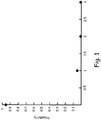
Fig. 1 is a chart depicting the probability of finding up to three photo-acid generators in a one cubic nanometer cell. -
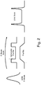
Fig. 2 graphically depicts the line scan that is created by scanning an electron beam across the profile of a feature such as a line of photoresist. -
Fig. 3 depicts the Z axis and normal lines as oriented by the sidewall of a feature such as a line of photoresist. -
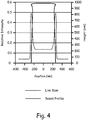
Fig. 4 depicts a simulated line scan according to an embodiment of the present invention. -
Fig. 5 is a flow chart for a method according to an embodiment of the present invention. - Various embodiments of the present method enable important lithographic phenomena to be studied, such as:
- 1. Critical dimension uniformity,
- 2. Line-edge roughness, line-width roughness, and associated power versus frequency spectra,
- 3. Photon shot noise effects and uncertainty in receiving the expected dose,
- 4. Acid generation mechanisms, acid distribution, acid diffusivity, and associated effects on photoresist performance,
- 5. Photoacid generator loading, distribution, and effects on performance, and
- 6. Quencher loading, distribution, diffusion, and effects on performance.
- Various embodiments of the present invention can be used to predict such statistical lithographic properties of a resist relief image as they would appear in actual CDSEM experiments. Various embodiments employ a combination of two simulation methods to produce a desired simulated result. The two methods that are combined include (1) a stochastic resist modeling method, and (2) a CDSEM image modeling method.
- Generally, the stochastic resist modeling method simulates the physical-chemical formation of the resist relief image, such that several statistical lithographic properties of the relief image can be studied as a response of the input. The CDSEM image modeling method then processes the output of the stochastic resist model using a physical model that approximates the interaction of an electron beam with the relief image. The final output is a highly realistic - but simulated - image of the resist relief as it would be viewed and measured by an actual CDSEM.
- The various methods for computer modeling of optical lithography processes usually follow a continuum approximation, which is the use of continuous mathematics to describe the average behavior. However, some events do not model well in a continuous domain, especially when considered in a very small volume. For example, light has a dual character in wave and quantum theory. The molecules that make up a photoresist layer are discrete. Chemical reactions are discrete and probabilistic. When describing behavior at length scales of tens of nanometers, an alternate approach to continuum modeling is to build the quantization of light and matter directly into the models, in what is called stochastic physical modeling, which uses probability distributions and random numbers to describe the statistical fluctuations that are expected.
- This method allows a researcher to model lithographic conditions that cannot be modeled with a continuum model, such as line-width roughness (the fluctuation of the critical dimension along a resist line), line-edge roughness (the fluctuation of the placement of the resist line edge), critical dimension variability, critical shape variability, the probability of forming certain defects, and so forth.
- This method also produces models that more closely approximate the formulation of actual resist. In this manner, the effects of photo-acid generator loading, photo-acid generator absorbance, photo-acid generator quantum efficiency, quencher loading, photon shot noise, and so forth on the photoresist relief image can be studied. Macro effects, such as the overall quantum yield of the exposure process can also be studied.
- Stochastic resist modeling is more useful for critical dimensions that are no greater than about one hundred nanometers. Such critical dimensions are routinely encountered in ArF immersion lithography, ArF double-patterning lithography, and extreme ultraviolet lithography.
- The embodiments according to the present invention comprehend statistical fluctuations that occur during the exposure process, since the state of the acid image in the resist after exposure (the acid shot noise image) strongly influences later behavior of the photoresist relief, such as line width roughness, line edge roughness, critical dimension variability, contact hole circularity, and so forth.
- As depicted in the flow chart of one
embodiment 10 ofFig. 5 , the first step is to specify a desired building-block volume of photoresist, within which the basic computations will be performed, as given inblock 12. Next, the number of acid generators and quenchers within this basic building-block volume are specified, as given inblock 14. This number is dependent upon the type of photoresist that is to be modeled, and can reflect either an actual photoresist product, or a theoretical photoresist product. The refractive index and irradiance of the photoresist are computed or specified, as desired, as given inblock 16. Again, these values can reflect either an actual photoresist product or a theoretical product. - The next step is to perform statistical computations on the number of absorbed photons, as given in block 18, because resists (specifically acid generators) are activated by the energy that is absorbed from the photons delivered during the exposure process. The average number of photons absorbed by a volume V with absorbance coefficient alpha is given by:

where α is the absorbance of the photoresist, I is the intensity of the light used in the exposure, t is the exposure time, λ is the actinic wavelength, V is the volume of interest, c is the vacuum velocity of light, and h is Planck's constant. Thus, the average number of absorbed photons is proportional to wavelength, absorbance, dose (It) and volume. For example, about fourteen times more photons are absorbed during an ArF emission exposure, as compared to an extreme ultraviolet emission exposure, even though the absorbed dose is constant in the two examples. - The Poisson probability distribution can be used, for example, to model the counting statistics of the number of absorbed photons. The probability of observing k successful photon absorption events given the average number of absorbed photons is:

- The properties of the Poisson distribution include the fact that the variance of the distribution is equal to the mean:


- The relative uncertainty of absorbing the expected number of photons (the expected dose) is:

- This indicates that the relative uncertainty of observing the average number of absorbed photons rises as the average number of absorbed photons decreases - a phenomenon known as shot noise. For example, at ten millijoules per square centimeter and with an alpha of four per micron, the standard deviation of the number of absorbed photons with an ArF emission is about 1.7 times the mean number of absorbed photons. With an extreme ultraviolet emission, the standard deviation of the number of absorbed photons is about 6.4 times the mean number of absorbed photons.
- The Poisson distribution can also be used to describe photoresist molecule counting statistics, such as the dispersion of discrete acid generators in a chemically-amplified resist film.
Fig. 1 indicates the probability of finding n acid generators in a cubic volume having a size of one nanometer on a side when the acid generator loading is five percent of the resist solids. It is interesting to note that, in this example, ninety-five percent of all of the one cubic nanometer cells contain no photo-acid generators. - The individual acid generator molecules that are dispersed throughout a chemically-amplified photoresist layer are activated by absorbing energy from the photons received by the photoresist during exposure. The interaction of the generated acids with the resin polymer in the photoresist eventually produces soluble regions in the film, after processing the resist through a post-exposure bake and development in an aqueous base. Therefore, the statistics of the generated acids are of great importance to the properties of the resist relief image, because acids are the primary imprint of the optical projection image (the initial condition).
- The stochastic resist models according to various embodiments of the present invention consider two probabilistic acid generator activation mechanisms. The first mechanism is direct photolysis, and the second mechanism is scattered low-energy electrons. A determination is made, as given in
block 20, as to which mechanism is the more appropriate. If a photolysis mechanism is more appropriate, then the number of acid generators that are converted to acid by photolysis is calculated, as described below and given inblock 24 ofFig. 5 . If the ionization mechanism is more appropriate, then the number of acid generators that are converted to acid by ionization is calculated, as described below and given in block 22 ofFig. 5 . In some embodiments both of the calculations are performed. - For the photolysis mechanism, the acid generators in the resist are activated by an absorbed photon with a probability that is equal to the quantum efficiency. At most, one acid is produced by the absorption of one photon. This is the most likely mechanism when the resist is irradiated by ArF light (wavelength of 193 nanometers). The distribution of the number of acids generated by direct photolysis and the effect upon the resist relief image is thus studied with stochastic resist simulation.
- For the ionization mechanism, the acid generators are activated by scattered low-energy electrons. Similar to the photoelectric effect, low energy electrons can be produced by ionization of the resist upon absorbance of high-energy extreme ultraviolet photons. The energy deposited in the resist film can, in this manner, activate acid generators some distance from the photon absorption site. This is the most likely mechanism for acid generation upon irradiation by extreme ultraviolet light (wavelength of 13.5 nanometers). However, the distribution of the number of acids produced via ionization is somewhat less predictable than the direct photolysis mechanism, because the photoelectron exposure mechanism allows a single photon to generate multiple electrons, and each electron may then travel through the resist film, activating multiple acid generators. Therefore, more than one acid may be generated per photon absorption event.
- In various embodiments, the ionization process is modeled as a two-step mechanism, and each step is a stochastic process. The probability of generating a specific number of acids is modeled as the product of a conditional probability:


- Using one or both of these two activation methods, the number of acids is determined and entered into the mathematical model, as given in
block 26. Once this is accomplished, the resist reactions between the acids and the quenchers in the photoresist are calculated, as given in block 28. This produces a model of the photoresist that indicates which portions of the photoresist have been exposed, and to what degree. - Next, the development of the photoresist is computed, as given in
block 30. In this step, the effects of the developing solution upon the exposed portions of the photoresist, as previously calculated, are determined and entered into the model. - Once these steps have been accomplished, a three-dimensional graphical image of the photoresist can be produced, as given in
block 32. It is appreciated that other steps in the mathematical model development, such as accounting for temperature, humidity, bakes, and other events are also included in the mode, as desired. - The image produced in
step 32 looks just like a SEM image would, if a photograph were to be taken of an actual exposed and developed photoresist line pattern - including line edge and sidewall roughness, height variation, sidewall profile, overexposure, underexposure, and so forth. However, this image is produced mathematically instead of photographically - other than that, there are very few differences. But because an actual photoresist formulation does not have to be created, and actual processing conditions do not have to been applied to the process, a far greater number of conditions can be simulated in the present method, and in a shorter length of time, than in actual empirical studies. - Because of their high quality, repeatability, and non-destructive nature, CDSEMs are the gold standard for the metrology of the features that are produced by optical lithography processes. A method that models the CDSEM's effects is clearly useful in producing a more realistic simulation.
- Determining a critical dimension with a top-down scanning electron microscope begins with the creation of a line scan, or intensity signal from the secondary electron detector as the electron beam is scanned across the image. In practice, the line scan usually results from the averaging of several scans to reduce the noise in the signal. Once this is accomplished, a functional form is fit to the scan to make measurements between corresponding points, as depicted in
Fig. 2 . - An electron beam scans across the resist profile and secondary electrons that result from the interaction of the beam and material are collected in a detector. The secondary electrons come from a region that is typically no more than about five nanometers below the surface of the profile. Because the beam has a finite cross section, it illuminates a larger area on the profile side wall than on the horizontal surfaces, there is, therefore, a greater signal from the edges of the profile than from the center. If the beam were very thin and uniform, then the resulting intensity profile would appear quite square (ignoring extra electrons that escape from the corner regions of the profile). But because the beam actually has a Gaussian profile, the measured line scan appears as a convolution of the ideal square intensity profile with the Gaussian kernel.
- The simplest physical model that attains the goal of producing a better match to experiment than a constant offset is used. The starting point is noting that the intensity profile is a function of the angle between the surface normal and the z-axis, as depicted in
Fig. 3 . This function is at a maximum for vertical sidewalls (sidewall angle θ of ninety degrees) and a minimum for horizontal sidewalls (sidewall angle θ of zero degrees). The secant function can be used to model the intensity of the secondary electron signal:
- The secant function produces its minimum values for small angles, and ramps up to its maximum values for angles near ninety degrees.
- However, the sine function has a better behavior for nearly vertical sidewalls. The sine function is similar, though gentler in its rise toward its maximum value, resulting in a wider peak centered over the sidewalls. Note that the differences between these two distributions can be virtually scaled away in the final step. In addition to the angular dependence, the intensity can be adjusted to account for the fact that the resist material generally returns slightly more secondary electrons than the substrate, by simply changing the constant of proportionality for resist material and other materials. In other words, a constant offset is added to the intensity for portions of the curve that are covered by resist material. The final form of the intensity profile function is:


- A convolution of the ideal intensity profile is performed with a Gaussian kernel to arrive at a final simulated line scan, as depicted in
Fig. 4 . Adjusting the width of this Gaussian profile gives the desired scaling to the intensity profile mentioned above. The CDSEM metrology method is applied to the line scan to produce a critical dimension value, as given in block 34 ofFig. 5 . In some embodiments, only the mid critical dimension value is produced in the data that is produced. - Thus, various embodiments of the invention produce computer simulations of the resist relief image with a high degree of detail. Computer models of several statistical effects can be produced, such as line width roughness, line edge roughness, critical dimension variability, contact hole circularity - all as viewed and measured by the CDSEM. Computer modeling of certain forms of defectivity in the resist relief image are also possible. These embodiments enable scientists to replace costly empirical studies with less-expensive, highly-realistic, computer models.
- Some of these method embodiments are performed on processor-based equipment, such as personal computers or more specialized graphic processing computers. The output of these embodiments includes the graphical images of the photoresist profile and the tabulated critical dimension data in regard to the simulated SEM images. This information is used by process engineers and others to accomplish a number of different objectives as described elsewhere herein, and also including general objectives such as developing new photoresists, developing processing recipes, and performing initial qualification of photoresists and processes. Such information eventually leads to the processing of actual integrated circuits and other structures.
- The foregoing description of embodiments for this invention has been presented for purposes of illustration and description. It is not intended to be exhaustive or to limit the invention to the precise form disclosed. Obvious modifications or variations are possible in light of the above teachings. The embodiments are chosen and described in an effort to provide illustrations of the principles of the invention and its practical application, and to thereby enable one of ordinary skill in the art to utilize the invention in various embodiments and with various modifications as are suited to the particular use contemplated. All such modifications and variations are within the scope of the invention as determined by the appended claims when interpreted in accordance with the breadth to which they are fairly, legally, and equitably entitled.
Claims (8)
- A processor based method for measuring dimensional properties of a photoresist profile, the method comprising steps of:inputting photoresist and exposure parameters into a stochastic model of a photoresist process with the steps (14) and (16) of determining (14) a number of acid generators and quenchers within a photoresist volume;determining (16) a refractive index and irradiance of the photoresist volume; computing the photoresist profile from the stochastic model using the processor with the steps (18, 20, 22, 24, 28, 30, 32) of determining (18) a number of photons absorbed by the photoresist volume;determining (20) which one of a photolysis mechanism or an ionization mechanism is most appropriate and selecting either the photolysis mechanism or the ionization mechanism;determining (22, 24) a number of the acid generators converted to acid by the selected photolysis mechanism or ionization mechanism;calculating (28) resist reactions between the acid generators and the quenchers in the photoresist volume which produces a model of the photoresist that indicates which portions of the photoresist has been exposed and to what degree;calculating (30) a development of the photoresist volume which determines the effects of a developing solution upon the exposed portions of the photoresist;producing (32) with the processor a three-dimensional simulated scanning electron microscope image of the photoresist profile created by the development of the photoresist volume;measuring (34) the dimensional properties of the photoresist profile using a CDSEM simulator running on the processor; andspecifying processes for fabricating integrated circuits based at least on the dimensional properties of the photoresist profile.
- The method of claim 1, wherein the step of determining the number of acid generators and quenchers within the photoresist volume comprises specifying a desired number of acid generators and specifying a desired number of quenchers based on a hypothetical photoresist formulation.
- The method of claim 1, wherein the step of determining the number of acid generators and quenchers within the photoresist volume comprises entering an actual number of acid generators and an actual number of quenchers based on an existing photoresist formulation.
- The method of claim 1, wherein the step of determining the number of photons absorbed by the photoresist volume comprises specifying a desired number of photons based on a hypothetical exposure.
- The method of claim 1, wherein the step of determining the number of photons absorbed by the photoresist volume comprises entering the number of photons based on a known exposure.
- The method of claim 1, wherein the step of measuring the dimensional properties of the photoresist profile comprises measuring a hard-copy output of the three- dimensional simulated scanning electron microscope image with a ruler.
- The method of claim 1, wherein the step of measuring the dimensional properties of the photoresist profile comprises mathematically evaluating a data file of the three-dimensional simulated scanning electron microscope image.
- A computer readable medium having instruction modules disposed thereon, where the instruction modules are not transitory signals, the instruction modules for instructing a processor to measure dimensional properties of a photoresist profile, the instruction modules operable for:determining (14) a number of acid generators and quenchers within a photoresist volume;determining (16) a refractive index and irradiance of the photoresist volume;determining (18) a number of photons absorbed by the photoresist volume;determining (20) which one of a photolysis mechanism or an ionization mechanism is most appropriate and selecting either the photolysis mechanism or the ionization mechanism;determining (22, 24) a number of the acid generators converted to acid by the selected photolysis mechanism or ionization mechanism;determining a number of acid and quencher reactions within the photoresist volume;calculating (28) resist reactions between the acid generators and the quenchers in the photoresist volume which produces a model of the photoresist that indicates which portions of the photoresist has been exposed and to what degree;calculating a development of the photoresist volume which determines the effects of a developing solution upon the exposed portions of the photoresist;producing with the processor a three-dimensional simulated scanning electron microscope image of the photoresist profile created by the development of the photoresist volume;measuring the dimensional properties of the photoresist profile using a CDSEM simulator running on the processor; andspecifying processes for fabricating integrated circuits based at least on the dimensional properties of the photoresist profile.
Applications Claiming Priority (3)
| Application Number | Priority Date | Filing Date | Title |
|---|---|---|---|
| US26053309P | 2009-11-12 | 2009-11-12 | |
| US12/915,455 US8589827B2 (en) | 2009-11-12 | 2010-10-29 | Photoresist simulation |
| PCT/US2010/055937 WO2011059947A2 (en) | 2009-11-12 | 2010-11-09 | Photoresist simulation |
Publications (3)
| Publication Number | Publication Date |
|---|---|
| EP2499661A2 EP2499661A2 (en) | 2012-09-19 |
| EP2499661A4 EP2499661A4 (en) | 2014-03-05 |
| EP2499661B1 true EP2499661B1 (en) | 2018-08-08 |
Family
ID=43974826
Family Applications (1)
| Application Number | Title | Priority Date | Filing Date |
|---|---|---|---|
| EP10830578.0A Active EP2499661B1 (en) | 2009-11-12 | 2010-11-09 | Photoresist simulation |
Country Status (5)
| Country | Link |
|---|---|
| US (2) | US8589827B2 (en) |
| EP (1) | EP2499661B1 (en) |
| JP (1) | JP5719850B2 (en) |
| KR (1) | KR101454522B1 (en) |
| WO (1) | WO2011059947A2 (en) |
Families Citing this family (23)
| Publication number | Priority date | Publication date | Assignee | Title |
|---|---|---|---|---|
| US8589827B2 (en) * | 2009-11-12 | 2013-11-19 | Kla-Tencor Corporation | Photoresist simulation |
| NL2009982A (en) | 2012-01-10 | 2013-07-15 | Asml Netherlands Bv | Source mask optimization to reduce stochastic effects. |
| KR101362326B1 (en) * | 2012-08-06 | 2014-02-24 | 현대모비스 주식회사 | Rear camera system for vehicle having parking alignment function and parking guide system using the same |
| WO2015127459A1 (en) | 2014-02-24 | 2015-08-27 | Tokyo Electron Limited | Methods and techniques to use with photosensitized chemically amplified resist chemicals and processes |
| JP6895600B2 (en) | 2014-02-25 | 2021-06-30 | 東京エレクトロン株式会社 | Chemical Amplification Methods and Techniques for Developable Bottom Anti-Reflective Coatings and Colored Implant Resists |
| US9733576B2 (en) | 2014-03-17 | 2017-08-15 | Kla-Tencor Corporation | Model for accurate photoresist profile prediction |
| CN103887199B (en) * | 2014-03-20 | 2017-01-11 | 上海华力微电子有限公司 | Method for detecting photoresist damage through dark-field silicon wafer detection machine |
| US10453748B2 (en) * | 2015-08-27 | 2019-10-22 | Micron Technology, Inc. | Methods of forming semiconductor device structures including stair step structures |
| US10429745B2 (en) * | 2016-02-19 | 2019-10-01 | Osaka University | Photo-sensitized chemically amplified resist (PS-CAR) simulation |
| US10048594B2 (en) | 2016-02-19 | 2018-08-14 | Tokyo Electron Limited | Photo-sensitized chemically amplified resist (PS-CAR) model calibration |
| KR102475021B1 (en) | 2016-05-13 | 2022-12-06 | 도쿄엘렉트론가부시키가이샤 | Critical dimension control by use of photosensitive chemicals or photosensitive chemically amplified resists |
| CN109313395B (en) | 2016-05-13 | 2021-05-14 | 东京毅力科创株式会社 | Critical dimension control through the use of light agents |
| CN110050230B (en) * | 2016-12-02 | 2021-06-11 | Asml荷兰有限公司 | Model for estimating random variables |
| FR3060752B1 (en) * | 2016-12-15 | 2019-05-10 | Commissariat A L'energie Atomique Et Aux Energies Alternatives | METHOD FOR IMPLEMENTING A CD-SEM CHARACTERIZATION TECHNIQUE |
| US10474042B2 (en) * | 2017-03-22 | 2019-11-12 | Kla-Tencor Corporation | Stochastically-aware metrology and fabrication |
| KR102380916B1 (en) | 2017-05-12 | 2022-04-01 | 에이에스엠엘 네델란즈 비.브이. | Methods for evaluating resist development |
| US11493850B2 (en) | 2019-07-23 | 2022-11-08 | Samsung Electronics Co., Ltd. | Lithography method using multi-scale simulation, semiconductor device manufacturing method and exposure equipment |
| WO2021034567A1 (en) | 2019-08-16 | 2021-02-25 | Tokyo Electron Limited | Method and process for stochastic driven defectivity healing |
| JP7310466B2 (en) * | 2019-09-10 | 2023-07-19 | 株式会社ニューフレアテクノロジー | Multi-charged particle beam evaluation method |
| JP6832463B1 (en) * | 2020-04-06 | 2021-02-24 | 東京応化工業株式会社 | Information processing system, information processing device, information processing method and program |
| TW202211075A (en) * | 2020-06-05 | 2022-03-16 | 美商新思科技股份有限公司 | Calibrating stochastic signals in compact modeling |
| KR20220149823A (en) * | 2021-04-30 | 2022-11-09 | 삼성전자주식회사 | Lithography method using multi-scale simulation, and method of manufacturing semiconductor device and exposure equipment based on the lithography method |
| CN114488705A (en) * | 2022-01-13 | 2022-05-13 | 东方晶源微电子科技(北京)有限公司 | Negative developing photoresist model optimization method |
Family Cites Families (19)
| Publication number | Priority date | Publication date | Assignee | Title |
|---|---|---|---|---|
| US6078738A (en) * | 1997-05-08 | 2000-06-20 | Lsi Logic Corporation | Comparing aerial image to SEM of photoresist or substrate pattern for masking process characterization |
| JP2971434B2 (en) * | 1998-03-19 | 1999-11-08 | 株式会社東芝 | Chemically amplified resist, method of manufacturing the same, pattern forming method and exposure simulation method |
| JP3564298B2 (en) | 1998-06-18 | 2004-09-08 | 株式会社東芝 | Pattern evaluation method and pattern generation method using computer |
| JP2001135567A (en) * | 1999-11-08 | 2001-05-18 | Semiconductor Leading Edge Technologies Inc | Apparatus and method for simulating shape of resist pattern and recording medium |
| JP2002006498A (en) * | 2000-06-27 | 2002-01-09 | Shin Etsu Chem Co Ltd | Method for predicting characteristic in chemical amplification resist material |
| JP2002287360A (en) * | 2001-03-27 | 2002-10-03 | Sony Corp | Method for designing photosensitive composition and lithographic method |
| JP2003068625A (en) * | 2001-08-29 | 2003-03-07 | Nikon Corp | Method of simulating shape of resist pattern |
| KR20050065164A (en) * | 2003-12-24 | 2005-06-29 | 주식회사 하이닉스반도체 | Inspection method for side profile of photo resist pattern |
| US7025280B2 (en) | 2004-01-30 | 2006-04-11 | Tokyo Electron Limited | Adaptive real time control of a reticle/mask system |
| JP2007523373A (en) * | 2004-02-23 | 2007-08-16 | コーニンクレッカ フィリップス エレクトロニクス エヌ ヴィ | Determination of image blur in image system |
| US7116411B2 (en) * | 2004-08-26 | 2006-10-03 | Asml Masktools B.V. | Method of performing resist process calibration/optimization and DOE optimization for providing OPE matching between different lithography systems |
| KR20060103972A (en) * | 2005-03-29 | 2006-10-09 | 삼성전자주식회사 | Method for inspecting a profile of minute structures |
| US7378202B2 (en) * | 2006-02-21 | 2008-05-27 | Mentor Graphics Corporation | Grid-based resist simulation |
| JP2008091721A (en) * | 2006-10-03 | 2008-04-17 | Toshiba Corp | Resist pattern prediction system, method for predicting resist pattern, and method for correcting mask pattern |
| US7949618B2 (en) * | 2007-03-28 | 2011-05-24 | Tokyo Electron Limited | Training a machine learning system to determine photoresist parameters |
| WO2010046408A2 (en) * | 2008-10-22 | 2010-04-29 | Micronic Laser Systems Ab | Method of iterative compensation for non-linear effects in three-dimensional exposure of resist |
| US8589827B2 (en) * | 2009-11-12 | 2013-11-19 | Kla-Tencor Corporation | Photoresist simulation |
| US8336003B2 (en) * | 2010-02-19 | 2012-12-18 | International Business Machines Corporation | Method for designing optical lithography masks for directed self-assembly |
| US8108805B2 (en) * | 2010-03-26 | 2012-01-31 | Tokyo Electron Limited | Simplified micro-bridging and roughness analysis |
-
2010
- 2010-10-29 US US12/915,455 patent/US8589827B2/en active Active
- 2010-11-09 WO PCT/US2010/055937 patent/WO2011059947A2/en active Application Filing
- 2010-11-09 JP JP2012538879A patent/JP5719850B2/en active Active
- 2010-11-09 EP EP10830578.0A patent/EP2499661B1/en active Active
- 2010-11-09 KR KR1020127013240A patent/KR101454522B1/en active IP Right Grant
-
2013
- 2013-08-28 US US14/011,989 patent/US9679116B2/en active Active
Non-Patent Citations (1)
| Title |
|---|
| CHRIS A MACK: "30 Years of Lithography Simulation", 1 January 2005 (2005-01-01), XP055249922, Retrieved from the Internet <URL:http://www.lithoguru.com/scientist/litho_papers/2005_Thirty_Years_of_Lithography_Simulation.pdf> [retrieved on 20160215] * |
Also Published As
| Publication number | Publication date |
|---|---|
| JP5719850B2 (en) | 2015-05-20 |
| US20140067346A1 (en) | 2014-03-06 |
| EP2499661A4 (en) | 2014-03-05 |
| WO2011059947A3 (en) | 2011-10-13 |
| US20110112809A1 (en) | 2011-05-12 |
| WO2011059947A2 (en) | 2011-05-19 |
| EP2499661A2 (en) | 2012-09-19 |
| US9679116B2 (en) | 2017-06-13 |
| KR101454522B1 (en) | 2014-10-24 |
| JP2013511152A (en) | 2013-03-28 |
| US8589827B2 (en) | 2013-11-19 |
| KR20120085841A (en) | 2012-08-01 |
Similar Documents
| Publication | Publication Date | Title |
|---|---|---|
| EP2499661B1 (en) | Photoresist simulation | |
| Brainard et al. | Shot noise, LER, and quantum efficiency of EUV photoresists | |
| CN109073985B (en) | Photosensitive chemically amplified resist (PS-CAR) model calibration | |
| CN109073984B (en) | Photosensitive chemically amplified resist (PS-CAR) simulation | |
| Biafore et al. | Statistical simulation of resist at EUV and ArF | |
| Houle et al. | Influence of resist components on image blur in a patterned positive-tone chemically amplified photoresist | |
| US11415897B2 (en) | Calibrating stochastic signals in compact modeling | |
| Santaclara et al. | One metric to rule them all: new k4 definition for photoresist characterization | |
| Maas et al. | Stochastics in extreme ultraviolet lithography: investigating the role of microscopic resist properties for metal-oxide-based resists | |
| Gao et al. | Calibration and verification of a stochastic model for EUV resist | |
| Biafore et al. | Application of stochastic modeling to resist optimization problems | |
| Thackeray et al. | Pursuit of lower Critical Dimensional Uniformity in EUV resists | |
| Gronheid et al. | Extreme-ultraviolet secondary electron blur at the 22-nm half pitch node | |
| Fukuda | Localized and cascading secondary electron generation as causes of stochastic defects in extreme ultraviolet projection lithography | |
| Wei et al. | Calibration and application of Gaussian random field models for exposure and resist stochastic in EUV lithography | |
| Bunday et al. | Phenomenology of electron-beam-induced photoresist shrinkage trends | |
| Chunder et al. | Separating the optical contributions to line-edge roughness in EUV lithography using stochastic simulations | |
| Jin et al. | Estimation of effective reaction radius for catalytic chain reaction of chemically amplified resist by Bayesian optimization | |
| Kostic et al. | Experimental and theoretical study on chemically semi-amplified resist AR-P 6200 | |
| Schnattinger et al. | A comprehensive resist model for the prediction of line-edge roughness material and process dependencies in optical lithography | |
| Fukuda | Stochastic defect generation in EUV lithography analyzed by spatially correlated probability model, reaction-limited and scattering-limited? | |
| Leunissen et al. | Determining the impact of statistical fluctuations on resist line edge roughness | |
| Mack et al. | Stochastic exposure kinetics of EUV photoresists: a simulation study | |
| Chunder et al. | Systematic assessment of the contributors of line edge roughness in EUV lithography using simulations | |
| Hudek et al. | Multi-beam mask writer exposure optimization for EUV mask stacks |
Legal Events
| Date | Code | Title | Description |
|---|---|---|---|
| PUAI | Public reference made under article 153(3) epc to a published international application that has entered the european phase |
Free format text: ORIGINAL CODE: 0009012 |
|
| 17P | Request for examination filed |
Effective date: 20120612 |
|
| AK | Designated contracting states |
Kind code of ref document: A2 Designated state(s): AL AT BE BG CH CY CZ DE DK EE ES FI FR GB GR HR HU IE IS IT LI LT LU LV MC MK MT NL NO PL PT RO RS SE SI SK SM TR |
|
| DAX | Request for extension of the european patent (deleted) | ||
| RIC1 | Information provided on ipc code assigned before grant |
Ipc: G03C 5/00 20060101ALI20140120BHEP Ipc: H01L 21/30 20060101AFI20140120BHEP Ipc: H01L 21/027 20060101ALI20140120BHEP |
|
| A4 | Supplementary search report drawn up and despatched |
Effective date: 20140130 |
|
| 17Q | First examination report despatched |
Effective date: 20160330 |
|
| GRAP | Despatch of communication of intention to grant a patent |
Free format text: ORIGINAL CODE: EPIDOSNIGR1 |
|
| STAA | Information on the status of an ep patent application or granted ep patent |
Free format text: STATUS: GRANT OF PATENT IS INTENDED |
|
| INTG | Intention to grant announced |
Effective date: 20180221 |
|
| GRAS | Grant fee paid |
Free format text: ORIGINAL CODE: EPIDOSNIGR3 |
|
| GRAA | (expected) grant |
Free format text: ORIGINAL CODE: 0009210 |
|
| STAA | Information on the status of an ep patent application or granted ep patent |
Free format text: STATUS: THE PATENT HAS BEEN GRANTED |
|
| AK | Designated contracting states |
Kind code of ref document: B1 Designated state(s): AL AT BE BG CH CY CZ DE DK EE ES FI FR GB GR HR HU IE IS IT LI LT LU LV MC MK MT NL NO PL PT RO RS SE SI SK SM TR |
|
| REG | Reference to a national code |
Ref country code: GB Ref legal event code: FG4D |
|
| REG | Reference to a national code |
Ref country code: CH Ref legal event code: EP Ref country code: AT Ref legal event code: REF Ref document number: 1027966 Country of ref document: AT Kind code of ref document: T Effective date: 20180815 |
|
| REG | Reference to a national code |
Ref country code: IE Ref legal event code: FG4D |
|
| REG | Reference to a national code |
Ref country code: DE Ref legal event code: R096 Ref document number: 602010052637 Country of ref document: DE |
|
| REG | Reference to a national code |
Ref country code: NL Ref legal event code: FP |
|
| REG | Reference to a national code |
Ref country code: LT Ref legal event code: MG4D |
|
| REG | Reference to a national code |
Ref country code: AT Ref legal event code: MK05 Ref document number: 1027966 Country of ref document: AT Kind code of ref document: T Effective date: 20180808 |
|
| PG25 | Lapsed in a contracting state [announced via postgrant information from national office to epo] |
Ref country code: GR Free format text: LAPSE BECAUSE OF FAILURE TO SUBMIT A TRANSLATION OF THE DESCRIPTION OR TO PAY THE FEE WITHIN THE PRESCRIBED TIME-LIMIT Effective date: 20181109 Ref country code: BG Free format text: LAPSE BECAUSE OF FAILURE TO SUBMIT A TRANSLATION OF THE DESCRIPTION OR TO PAY THE FEE WITHIN THE PRESCRIBED TIME-LIMIT Effective date: 20181108 Ref country code: SE Free format text: LAPSE BECAUSE OF FAILURE TO SUBMIT A TRANSLATION OF THE DESCRIPTION OR TO PAY THE FEE WITHIN THE PRESCRIBED TIME-LIMIT Effective date: 20180808 Ref country code: NO Free format text: LAPSE BECAUSE OF FAILURE TO SUBMIT A TRANSLATION OF THE DESCRIPTION OR TO PAY THE FEE WITHIN THE PRESCRIBED TIME-LIMIT Effective date: 20181108 Ref country code: AT Free format text: LAPSE BECAUSE OF FAILURE TO SUBMIT A TRANSLATION OF THE DESCRIPTION OR TO PAY THE FEE WITHIN THE PRESCRIBED TIME-LIMIT Effective date: 20180808 Ref country code: PL Free format text: LAPSE BECAUSE OF FAILURE TO SUBMIT A TRANSLATION OF THE DESCRIPTION OR TO PAY THE FEE WITHIN THE PRESCRIBED TIME-LIMIT Effective date: 20180808 Ref country code: LT Free format text: LAPSE BECAUSE OF FAILURE TO SUBMIT A TRANSLATION OF THE DESCRIPTION OR TO PAY THE FEE WITHIN THE PRESCRIBED TIME-LIMIT Effective date: 20180808 Ref country code: IS Free format text: LAPSE BECAUSE OF FAILURE TO SUBMIT A TRANSLATION OF THE DESCRIPTION OR TO PAY THE FEE WITHIN THE PRESCRIBED TIME-LIMIT Effective date: 20181208 Ref country code: RS Free format text: LAPSE BECAUSE OF FAILURE TO SUBMIT A TRANSLATION OF THE DESCRIPTION OR TO PAY THE FEE WITHIN THE PRESCRIBED TIME-LIMIT Effective date: 20180808 Ref country code: FI Free format text: LAPSE BECAUSE OF FAILURE TO SUBMIT A TRANSLATION OF THE DESCRIPTION OR TO PAY THE FEE WITHIN THE PRESCRIBED TIME-LIMIT Effective date: 20180808 |
|
| PG25 | Lapsed in a contracting state [announced via postgrant information from national office to epo] |
Ref country code: AL Free format text: LAPSE BECAUSE OF FAILURE TO SUBMIT A TRANSLATION OF THE DESCRIPTION OR TO PAY THE FEE WITHIN THE PRESCRIBED TIME-LIMIT Effective date: 20180808 Ref country code: HR Free format text: LAPSE BECAUSE OF FAILURE TO SUBMIT A TRANSLATION OF THE DESCRIPTION OR TO PAY THE FEE WITHIN THE PRESCRIBED TIME-LIMIT Effective date: 20180808 Ref country code: LV Free format text: LAPSE BECAUSE OF FAILURE TO SUBMIT A TRANSLATION OF THE DESCRIPTION OR TO PAY THE FEE WITHIN THE PRESCRIBED TIME-LIMIT Effective date: 20180808 |
|
| PG25 | Lapsed in a contracting state [announced via postgrant information from national office to epo] |
Ref country code: EE Free format text: LAPSE BECAUSE OF FAILURE TO SUBMIT A TRANSLATION OF THE DESCRIPTION OR TO PAY THE FEE WITHIN THE PRESCRIBED TIME-LIMIT Effective date: 20180808 Ref country code: IT Free format text: LAPSE BECAUSE OF FAILURE TO SUBMIT A TRANSLATION OF THE DESCRIPTION OR TO PAY THE FEE WITHIN THE PRESCRIBED TIME-LIMIT Effective date: 20180808 Ref country code: RO Free format text: LAPSE BECAUSE OF FAILURE TO SUBMIT A TRANSLATION OF THE DESCRIPTION OR TO PAY THE FEE WITHIN THE PRESCRIBED TIME-LIMIT Effective date: 20180808 Ref country code: CZ Free format text: LAPSE BECAUSE OF FAILURE TO SUBMIT A TRANSLATION OF THE DESCRIPTION OR TO PAY THE FEE WITHIN THE PRESCRIBED TIME-LIMIT Effective date: 20180808 Ref country code: ES Free format text: LAPSE BECAUSE OF FAILURE TO SUBMIT A TRANSLATION OF THE DESCRIPTION OR TO PAY THE FEE WITHIN THE PRESCRIBED TIME-LIMIT Effective date: 20180808 |
|
| REG | Reference to a national code |
Ref country code: DE Ref legal event code: R097 Ref document number: 602010052637 Country of ref document: DE |
|
| PG25 | Lapsed in a contracting state [announced via postgrant information from national office to epo] |
Ref country code: SK Free format text: LAPSE BECAUSE OF FAILURE TO SUBMIT A TRANSLATION OF THE DESCRIPTION OR TO PAY THE FEE WITHIN THE PRESCRIBED TIME-LIMIT Effective date: 20180808 Ref country code: SM Free format text: LAPSE BECAUSE OF FAILURE TO SUBMIT A TRANSLATION OF THE DESCRIPTION OR TO PAY THE FEE WITHIN THE PRESCRIBED TIME-LIMIT Effective date: 20180808 Ref country code: DK Free format text: LAPSE BECAUSE OF FAILURE TO SUBMIT A TRANSLATION OF THE DESCRIPTION OR TO PAY THE FEE WITHIN THE PRESCRIBED TIME-LIMIT Effective date: 20180808 |
|
| PLBE | No opposition filed within time limit |
Free format text: ORIGINAL CODE: 0009261 |
|
| STAA | Information on the status of an ep patent application or granted ep patent |
Free format text: STATUS: NO OPPOSITION FILED WITHIN TIME LIMIT |
|
| REG | Reference to a national code |
Ref country code: CH Ref legal event code: PL |
|
| 26N | No opposition filed |
Effective date: 20190509 |
|
| GBPC | Gb: european patent ceased through non-payment of renewal fee |
Effective date: 20181109 |
|
| PG25 | Lapsed in a contracting state [announced via postgrant information from national office to epo] |
Ref country code: LU Free format text: LAPSE BECAUSE OF NON-PAYMENT OF DUE FEES Effective date: 20181109 Ref country code: MC Free format text: LAPSE BECAUSE OF FAILURE TO SUBMIT A TRANSLATION OF THE DESCRIPTION OR TO PAY THE FEE WITHIN THE PRESCRIBED TIME-LIMIT Effective date: 20180808 |
|
| REG | Reference to a national code |
Ref country code: BE Ref legal event code: MM Effective date: 20181130 |
|
| REG | Reference to a national code |
Ref country code: IE Ref legal event code: MM4A |
|
| PG25 | Lapsed in a contracting state [announced via postgrant information from national office to epo] |
Ref country code: CH Free format text: LAPSE BECAUSE OF NON-PAYMENT OF DUE FEES Effective date: 20181130 Ref country code: LI Free format text: LAPSE BECAUSE OF NON-PAYMENT OF DUE FEES Effective date: 20181130 Ref country code: SI Free format text: LAPSE BECAUSE OF FAILURE TO SUBMIT A TRANSLATION OF THE DESCRIPTION OR TO PAY THE FEE WITHIN THE PRESCRIBED TIME-LIMIT Effective date: 20180808 |
|
| PG25 | Lapsed in a contracting state [announced via postgrant information from national office to epo] |
Ref country code: IE Free format text: LAPSE BECAUSE OF NON-PAYMENT OF DUE FEES Effective date: 20181109 Ref country code: FR Free format text: LAPSE BECAUSE OF NON-PAYMENT OF DUE FEES Effective date: 20181130 |
|
| PG25 | Lapsed in a contracting state [announced via postgrant information from national office to epo] |
Ref country code: BE Free format text: LAPSE BECAUSE OF NON-PAYMENT OF DUE FEES Effective date: 20181130 |
|
| PG25 | Lapsed in a contracting state [announced via postgrant information from national office to epo] |
Ref country code: GB Free format text: LAPSE BECAUSE OF NON-PAYMENT OF DUE FEES Effective date: 20181109 |
|
| PG25 | Lapsed in a contracting state [announced via postgrant information from national office to epo] |
Ref country code: MT Free format text: LAPSE BECAUSE OF NON-PAYMENT OF DUE FEES Effective date: 20181109 |
|
| PG25 | Lapsed in a contracting state [announced via postgrant information from national office to epo] |
Ref country code: TR Free format text: LAPSE BECAUSE OF FAILURE TO SUBMIT A TRANSLATION OF THE DESCRIPTION OR TO PAY THE FEE WITHIN THE PRESCRIBED TIME-LIMIT Effective date: 20180808 |
|
| PG25 | Lapsed in a contracting state [announced via postgrant information from national office to epo] |
Ref country code: PT Free format text: LAPSE BECAUSE OF FAILURE TO SUBMIT A TRANSLATION OF THE DESCRIPTION OR TO PAY THE FEE WITHIN THE PRESCRIBED TIME-LIMIT Effective date: 20180808 |
|
| PG25 | Lapsed in a contracting state [announced via postgrant information from national office to epo] |
Ref country code: HU Free format text: LAPSE BECAUSE OF FAILURE TO SUBMIT A TRANSLATION OF THE DESCRIPTION OR TO PAY THE FEE WITHIN THE PRESCRIBED TIME-LIMIT; INVALID AB INITIO Effective date: 20101109 Ref country code: CY Free format text: LAPSE BECAUSE OF FAILURE TO SUBMIT A TRANSLATION OF THE DESCRIPTION OR TO PAY THE FEE WITHIN THE PRESCRIBED TIME-LIMIT Effective date: 20180808 Ref country code: MK Free format text: LAPSE BECAUSE OF NON-PAYMENT OF DUE FEES Effective date: 20180808 |
|
| P01 | Opt-out of the competence of the unified patent court (upc) registered |
Effective date: 20230525 |
|
| PGFP | Annual fee paid to national office [announced via postgrant information from national office to epo] |
Ref country code: NL Payment date: 20231126 Year of fee payment: 14 |
|
| PGFP | Annual fee paid to national office [announced via postgrant information from national office to epo] |
Ref country code: DE Payment date: 20231129 Year of fee payment: 14 |