EP2498279A1 - Procédé de traitement d'une couche de nitrure de métal oxydée - Google Patents
Procédé de traitement d'une couche de nitrure de métal oxydée Download PDFInfo
- Publication number
- EP2498279A1 EP2498279A1 EP12157408A EP12157408A EP2498279A1 EP 2498279 A1 EP2498279 A1 EP 2498279A1 EP 12157408 A EP12157408 A EP 12157408A EP 12157408 A EP12157408 A EP 12157408A EP 2498279 A1 EP2498279 A1 EP 2498279A1
- Authority
- EP
- European Patent Office
- Prior art keywords
- metal
- layer
- plasma
- nitride layer
- nitride
- Prior art date
- Legal status (The legal status is an assumption and is not a legal conclusion. Google has not performed a legal analysis and makes no representation as to the accuracy of the status listed.)
- Granted
Links
Images
Classifications
-
- H—ELECTRICITY
- H10—SEMICONDUCTOR DEVICES; ELECTRIC SOLID-STATE DEVICES NOT OTHERWISE PROVIDED FOR
- H10P—GENERIC PROCESSES OR APPARATUS FOR THE MANUFACTURE OR TREATMENT OF DEVICES COVERED BY CLASS H10
- H10P95/00—Generic processes or apparatus for manufacture or treatments not covered by the other groups of this subclass
-
- C—CHEMISTRY; METALLURGY
- C23—COATING METALLIC MATERIAL; COATING MATERIAL WITH METALLIC MATERIAL; CHEMICAL SURFACE TREATMENT; DIFFUSION TREATMENT OF METALLIC MATERIAL; COATING BY VACUUM EVAPORATION, BY SPUTTERING, BY ION IMPLANTATION OR BY CHEMICAL VAPOUR DEPOSITION, IN GENERAL; INHIBITING CORROSION OF METALLIC MATERIAL OR INCRUSTATION IN GENERAL
- C23C—COATING METALLIC MATERIAL; COATING MATERIAL WITH METALLIC MATERIAL; SURFACE TREATMENT OF METALLIC MATERIAL BY DIFFUSION INTO THE SURFACE, BY CHEMICAL CONVERSION OR SUBSTITUTION; COATING BY VACUUM EVAPORATION, BY SPUTTERING, BY ION IMPLANTATION OR BY CHEMICAL VAPOUR DEPOSITION, IN GENERAL
- C23C14/00—Coating by vacuum evaporation, by sputtering or by ion implantation of the coating forming material
- C23C14/06—Coating by vacuum evaporation, by sputtering or by ion implantation of the coating forming material characterised by the coating material
- C23C14/0641—Nitrides
-
- C—CHEMISTRY; METALLURGY
- C23—COATING METALLIC MATERIAL; COATING MATERIAL WITH METALLIC MATERIAL; CHEMICAL SURFACE TREATMENT; DIFFUSION TREATMENT OF METALLIC MATERIAL; COATING BY VACUUM EVAPORATION, BY SPUTTERING, BY ION IMPLANTATION OR BY CHEMICAL VAPOUR DEPOSITION, IN GENERAL; INHIBITING CORROSION OF METALLIC MATERIAL OR INCRUSTATION IN GENERAL
- C23C—COATING METALLIC MATERIAL; COATING MATERIAL WITH METALLIC MATERIAL; SURFACE TREATMENT OF METALLIC MATERIAL BY DIFFUSION INTO THE SURFACE, BY CHEMICAL CONVERSION OR SUBSTITUTION; COATING BY VACUUM EVAPORATION, BY SPUTTERING, BY ION IMPLANTATION OR BY CHEMICAL VAPOUR DEPOSITION, IN GENERAL
- C23C14/00—Coating by vacuum evaporation, by sputtering or by ion implantation of the coating forming material
- C23C14/58—After-treatment
- C23C14/5826—Treatment with charged particles
-
- C—CHEMISTRY; METALLURGY
- C23—COATING METALLIC MATERIAL; COATING MATERIAL WITH METALLIC MATERIAL; CHEMICAL SURFACE TREATMENT; DIFFUSION TREATMENT OF METALLIC MATERIAL; COATING BY VACUUM EVAPORATION, BY SPUTTERING, BY ION IMPLANTATION OR BY CHEMICAL VAPOUR DEPOSITION, IN GENERAL; INHIBITING CORROSION OF METALLIC MATERIAL OR INCRUSTATION IN GENERAL
- C23C—COATING METALLIC MATERIAL; COATING MATERIAL WITH METALLIC MATERIAL; SURFACE TREATMENT OF METALLIC MATERIAL BY DIFFUSION INTO THE SURFACE, BY CHEMICAL CONVERSION OR SUBSTITUTION; COATING BY VACUUM EVAPORATION, BY SPUTTERING, BY ION IMPLANTATION OR BY CHEMICAL VAPOUR DEPOSITION, IN GENERAL
- C23C14/00—Coating by vacuum evaporation, by sputtering or by ion implantation of the coating forming material
- C23C14/58—After-treatment
- C23C14/5846—Reactive treatment
- C23C14/5853—Oxidation
-
- H—ELECTRICITY
- H10—SEMICONDUCTOR DEVICES; ELECTRIC SOLID-STATE DEVICES NOT OTHERWISE PROVIDED FOR
- H10W—GENERIC PACKAGES, INTERCONNECTIONS, CONNECTORS OR OTHER CONSTRUCTIONAL DETAILS OF DEVICES COVERED BY CLASS H10
- H10W20/00—Interconnections in chips, wafers or substrates
- H10W20/01—Manufacture or treatment
- H10W20/031—Manufacture or treatment of conductive parts of the interconnections
- H10W20/032—Manufacture or treatment of conductive parts of the interconnections of conductive barrier, adhesion or liner layers
- H10W20/052—Manufacture or treatment of conductive parts of the interconnections of conductive barrier, adhesion or liner layers by treatments not introducing additional elements therein
-
- H—ELECTRICITY
- H10—SEMICONDUCTOR DEVICES; ELECTRIC SOLID-STATE DEVICES NOT OTHERWISE PROVIDED FOR
- H10D—INORGANIC ELECTRIC SEMICONDUCTOR DEVICES
- H10D62/00—Semiconductor bodies, or regions thereof, of devices having potential barriers
- H10D62/80—Semiconductor bodies, or regions thereof, of devices having potential barriers characterised by the materials
- H10D62/83—Semiconductor bodies, or regions thereof, of devices having potential barriers characterised by the materials being Group IV materials, e.g. B-doped Si or undoped Ge
-
- H—ELECTRICITY
- H10—SEMICONDUCTOR DEVICES; ELECTRIC SOLID-STATE DEVICES NOT OTHERWISE PROVIDED FOR
- H10D—INORGANIC ELECTRIC SEMICONDUCTOR DEVICES
- H10D62/00—Semiconductor bodies, or regions thereof, of devices having potential barriers
- H10D62/80—Semiconductor bodies, or regions thereof, of devices having potential barriers characterised by the materials
- H10D62/85—Semiconductor bodies, or regions thereof, of devices having potential barriers characterised by the materials being Group III-V materials, e.g. GaAs
-
- H—ELECTRICITY
- H10—SEMICONDUCTOR DEVICES; ELECTRIC SOLID-STATE DEVICES NOT OTHERWISE PROVIDED FOR
- H10D—INORGANIC ELECTRIC SEMICONDUCTOR DEVICES
- H10D64/00—Electrodes of devices having potential barriers
- H10D64/60—Electrodes characterised by their materials
- H10D64/62—Electrodes ohmically coupled to a semiconductor
-
- H—ELECTRICITY
- H10—SEMICONDUCTOR DEVICES; ELECTRIC SOLID-STATE DEVICES NOT OTHERWISE PROVIDED FOR
- H10H—INORGANIC LIGHT-EMITTING SEMICONDUCTOR DEVICES HAVING POTENTIAL BARRIERS
- H10H20/00—Individual inorganic light-emitting semiconductor devices having potential barriers, e.g. light-emitting diodes [LED]
- H10H20/01—Manufacture or treatment
- H10H20/032—Manufacture or treatment of electrodes
-
- H—ELECTRICITY
- H10—SEMICONDUCTOR DEVICES; ELECTRIC SOLID-STATE DEVICES NOT OTHERWISE PROVIDED FOR
- H10H—INORGANIC LIGHT-EMITTING SEMICONDUCTOR DEVICES HAVING POTENTIAL BARRIERS
- H10H20/00—Individual inorganic light-emitting semiconductor devices having potential barriers, e.g. light-emitting diodes [LED]
- H10H20/80—Constructional details
- H10H20/83—Electrodes
- H10H20/832—Electrodes characterised by their material
-
- H—ELECTRICITY
- H10—SEMICONDUCTOR DEVICES; ELECTRIC SOLID-STATE DEVICES NOT OTHERWISE PROVIDED FOR
- H10W—GENERIC PACKAGES, INTERCONNECTIONS, CONNECTORS OR OTHER CONSTRUCTIONAL DETAILS OF DEVICES COVERED BY CLASS H10
- H10W20/00—Interconnections in chips, wafers or substrates
- H10W20/01—Manufacture or treatment
- H10W20/031—Manufacture or treatment of conductive parts of the interconnections
- H10W20/032—Manufacture or treatment of conductive parts of the interconnections of conductive barrier, adhesion or liner layers
- H10W20/038—Manufacture or treatment of conductive parts of the interconnections of conductive barrier, adhesion or liner layers covering conductive structures
-
- Y—GENERAL TAGGING OF NEW TECHNOLOGICAL DEVELOPMENTS; GENERAL TAGGING OF CROSS-SECTIONAL TECHNOLOGIES SPANNING OVER SEVERAL SECTIONS OF THE IPC; TECHNICAL SUBJECTS COVERED BY FORMER USPC CROSS-REFERENCE ART COLLECTIONS [XRACs] AND DIGESTS
- Y10—TECHNICAL SUBJECTS COVERED BY FORMER USPC
- Y10S—TECHNICAL SUBJECTS COVERED BY FORMER USPC CROSS-REFERENCE ART COLLECTIONS [XRACs] AND DIGESTS
- Y10S257/00—Active solid-state devices, e.g. transistors, solid-state diodes
- Y10S257/915—Active solid-state devices, e.g. transistors, solid-state diodes with titanium nitride portion or region
Definitions
- the present invention relates to a method of treating an oxidized metal nitride layer.
- the object of the present invention is to overcome the drawbacks of the techniques of the prior art by proposing in particular a low temperature treatment process, an oxidized metal nitride layer, allowing to remove at least partially, or even totally the oxide layer of said metal formed on the surface of the metal nitride layer, while ensuring a substantially uniform surface of the metal nitride layer once the oxide layer of said metal is removed.
- said metal oxide layer is eliminated by being chemically replaced (see oxidation) by said metal layer in step i, this metal layer then being chemically transformed (see reduction) in step ii in a nitride layer of said metal, the treatment process according to the invention being carried out at low temperature.
- the metal oxide layer once removed advantageously allows to obtain a second layer of metal nitride of substantially uniform thickness on the surface of the first layer of metal nitride.
- This uniformity of thickness is very advantageous especially in the case of the use of the metal nitride layer thus treated during the manufacture of light-emitting diodes. Indeed, this flatness makes it possible to guarantee good electrical resistivity properties, which are reflected in particular by a uniformly emitted light signal in the field of light-emitting diodes.
- At least the metal nitride layer covered by the oxide layer of said metal forms a stack of layers. Said layer stack formed by the first and second metal nitride layers remains stable to the ambient atmosphere.
- the stack of layers can be part of an assembly of elements comprising a slice a semiconductor substrate which is the initial layer on which is deposited all the constituent layers of the assembly. Between the wafer of said substrate and the oxidized metal nitride layer may be other layers and / or components.
- the layers of the invention are preferably thin layers of circular cross section.
- the thickness of these layers can range from a few angstroms to a few thousand angstroms.
- the total elimination of the metal oxide layer formed on the surface of the first metal nitride layer can be accomplished by consuming a portion of the first metal nitride layer in step ii.
- those skilled in the art can play on the operating conditions of step ii to minimize said consumption.
- the metal oxide layer is conventionally formed following certain delamination processes (known for angling " stripping ”) requiring an oxygen-based plasma.
- delamination processes known for angling " stripping ”
- oxygen plasma delamination O 2
- resin mask having been deposited on the first layer of metal nitride, during the manufacture of a metal electrode.
- metal electrode means a stack of several electrically conductive layers comprising at least one electrically conductive layer, such as for example an aluminum or copper layer, or a layer of a mixture of aluminum and copper, on which was deposited the first layer of metal nitride.
- the formation of a metal oxide layer on the surface of the first metal nitride layer is detrimental to the electrode since this metal oxide layer acts as an electrical barrier due to its electrical resistivity relative to said metal nitride layer.
- the first layer of metal nitride, deposited on the electrically conductive layer can be defined as a so-called electrically conductive encapsulation layer, and protecting the electrically conductive layer physicochemical interactions that may occur during the steps following the deposition of the electrically conductive layer.
- the treatment method according to the invention has the advantage of being able to be performed at low temperature in order to avoid any degradation of the components (eg transistors, resistors, etc.) constituting an assembly of elements comprising the oxidized titanium nitride layer to be treated, said components possibly having physical properties; degradation at temperatures above the "low temperature”.
- the temperatures of steps i and ii are in particular less than the degradation temperatures of the physicochemical properties of said components.
- steps i and ii of the treatment method according to the invention can be carried out at temperatures strictly below 400 ° C.
- step i is carried out at a temperature of at most 300 ° C, preferably at most 200 ° C, and more preferably at most 100 ° C.
- step ii is carried out at a temperature of at most 300 ° C, preferably at most 200 ° C, and more preferably at most 100 ° C.
- the first and second modes are combined.
- the steps i and ii according to the invention are preferably carried out in a plasma reactor comprising a sample holder.
- the temperatures mentioned in the present invention are those measured in the plasma reactor in which steps i and ii are carried out, and more particularly these temperatures are those of the sample holder on which is positioned the stack to be treated comprising the first layer of oxidized metal nitride.
- steps i and ii are preferably carried out in an inert atmosphere, or in other words in an oxygen-free atmosphere.
- steps i and ii can be carried out under a nitrogen atmosphere or under vacuum.
- the constituent metal of the metal nitride layer, the metal oxide layer, and the metal layer is the same metal.
- said metal belongs to the family of transition metals, and may advantageously be chosen from tantalum, titanium and tungsten, or a mixture thereof.
- the oxidizing species according to the invention may be a fluorine-based plasma (ie a plasma comprising fluorine).
- Nitrogen trifluoride (NF 3 ) may be mentioned in particular.
- the metal layer is a layer composed of metal fluoride.
- said metal fluoride is thus tantalum fluoride or titanium fluoride.
- the hydrogen and nitrogen plasma can be chosen from a plasma of a mixture of hydrogen and nitrogen; and an NH 3 plasma; or their mixture.
- the electron density, the bombardment energy, and the duration of the plasmas of steps i and ii are parameters well known to those skilled in the art for optimizing the chemical transformation of the layered metal oxide layer.
- metal step i
- the chemical transformation of the metal layer into a metal nitride layer step ii).
- steps i and ii there may be mentioned an electron density around 1.2 ⁇ 10 10 cm -3 , a bombardment energy of between 120 and 210 eV, and a duration of the order of 15 to 20s.
- Another object according to the invention relates to a stack of layers comprising said first metal nitride layer covered by said second nitride layer of said metal, said layers being obtained by the treatment method according to the present invention.
- This stack of two nitride layers of the same metal has the advantage of guaranteeing good properties of electrical resistivity, which is reflect in particular a uniformly emitted light signal in the field of light-emitting diodes.
- Another object according to the invention relates to a metal electrode comprising said first metal nitride layer covered by said second nitride layer of said metal, said layers being obtained by the treatment method according to the present invention.
- This metal electrode may be an anode, in particular used in the manufacture of light-emitting diodes, this anode permitting the transmission of light to the coloring filters in this type of technology.
- Another object according to the invention relates to a light-emitting diode comprising said first metal nitride layer covered by said second nitride layer of said metal, said layers obtained by the treatment method according to the present invention.
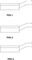
- the figure 1 represents a stack of at least two layers of circular cross section with a diameter of 200 mm, before the application of the treatment method according to the present invention.
- These two layers are a first layer of titanium nitride (1) with a thickness of 80 angstroms, the upper part of which is covered by a layer of titanium oxide (2), with a thickness of about 40 angstroms.
- the total thickness of these two layers is therefore 120 angstroms.
- Said stack is deposited on the sample holder of a plasma reactor marketed by Tokyo Electron Limited under the reference 85 SCCM.
- the first nitride layer is not directly in physical contact with the sample holder.
- Said stack is originally deposited on a wafer of a substrate of a semiconductor material (not shown in FIGS. Figures 1 to 3 ) such as silicon. Said stack is thus deposited on the sample holder via said substrate.
- the titanium oxide layer (2) is oxidized by a nitrogen trifluoride (NF 3 ) plasma to form titanium fluoride and nitrogen oxide.
- NF 3 nitrogen trifluoride
- the stacking of the figure 2 still comprising the first layer of titanium nitride (1) covered, either by the titanium oxide layer (2), but by a metal layer of titanium fluoride (3) of circular cross section.
- the titanium fluoride layer (3) is reduced by a plasma comprising a mixture of hydrogen (H 2 ) and nitrogen (N 2 ) to form titanium nitride and hydrofluoric acid.
- the stacking of the figure 3 still comprising the first layer of titanium nitride (1) coated, either by the titanium fluoride layer (3), but by a second layer of titanium nitride (4) of circular cross section.
- the thickness measurements of the layers in the context of the present invention were carried out by X-ray fluorescence using a Panalytical brand apparatus.
- the thickness variation over the entire surface of said layer was also measured by X-ray fluorescence using the same apparatus as mentioned above.
- the variation between the smallest measured thickness and the largest thickness measured over the total thickness of the stack formed by the first and second titanium nitride layers is only 14 angstroms, or in other words the thickness total is 67 angstroms plus or minus 7 angstroms, measured.
- the stacks represented on the Figures 1 to 3 are not limited to these two layers. Indeed, in the case of the manufacture of a metal electrode, the first metal nitride layer is typically deposited on an electrically conductive layer such as a layer of aluminum and / or copper (not shown in FIGS. Figures 1 to 3 ).
Landscapes
- Chemical & Material Sciences (AREA)
- Chemical Kinetics & Catalysis (AREA)
- Engineering & Computer Science (AREA)
- Materials Engineering (AREA)
- Mechanical Engineering (AREA)
- Metallurgy (AREA)
- Organic Chemistry (AREA)
- Electrodes Of Semiconductors (AREA)
- Led Devices (AREA)
Abstract
i. oxyder une couche (2) d'oxyde de métal à la surface d'une première couche (1) de nitrure dudit métal, à l'aide d'un plasma d'une espèce oxydante ayant un degré d'oxydation supérieur à celui de l'oxygène pour former une couche (3) métallique d'un composé à base dudit métal, et
ii. réduire la couche (3) métallique formée à l'étape i à l'aide d'un plasma d'hydrogène et d'azote, pour former une deuxième couche (4) de nitrure dudit métal.
Description
- La présente invention se rapporte à un procédé de traitement d'une couche de nitrure de métal oxydée.
- Elle s'applique typiquement, mais non exclusivement, à la fabrication d'électrodes métalliques, utilisées notamment dans la fabrication de diodes électroluminescentes.
- Du document
US 6 169 027 est connu un procédé de traitement consistant à éliminer la présence d'une couche d'oxyde de titane formée à la surface d'une couche de nitrure de titane, en appliquant un plasma d'hydrogène et d'azote à une température élevée. Ainsi, l'oxyde de titane est réduit par l'hydrogène pour former du nitrure de titane. - Toutefois, l'inconvénient de ce type de procédé est qu'il doit être réalisé à température élevée, c'est-à-dire à une température comprise entre 400 et 550°C.
- En effet, une température aussi élevée, nécessitée par le fait de réduire directement le nitrure de titane, ne permet pas de réaliser le procédé de l'art antérieur sur un assemblage d'éléments comprenant la couche de nitrure de titane, et d'autres couches et/ou composants (e.g. transistors, résistances, ...etc) dont les propriétés physico-chimiques se dégradent à température élevée, notamment à des températures supérieures à 400°C.
- Le but de la présente invention est de pallier les inconvénients des techniques de l'art antérieur en proposant notamment un procédé de traitement à basse température, d'une couche de nitrure de métal oxydée, permettant de supprimer au moins en partie, voire en totalité, la couche d'oxyde dudit métal formée à la surface de la couche de nitrure de métal, tout en garantissant une surface sensiblement uniforme de la couche de nitrure de métal une fois la couche d'oxyde dudit métal supprimée.
- La présente invention a pour objet un procédé de traitement d'une couche de nitrure de métal oxydée, comprenant les étapes consistant à :
- i. oxyder une couche d'oxyde de métal à la surface d'une première couche de nitrure dudit métal, à l'aide d'un plasma d'une espèce oxydante ayant un degré d'oxydation supérieur à celui de l'oxygène pour former une couche métallique d'un composé à base dudit métal, et
- ii. réduire la couche métallique formée à l'étape i à l'aide d'un plasma d'hydrogène et d'azote, pour former une deuxième couche de nitrure dudit métal.
- Grâce à la présente invention, ladite couche d'oxyde de métal est éliminée en étant remplacée chimiquement (cf. oxydation) par ladite couche métallique à l'étape i, cette couche métallique étant ensuite transformée chimiquement (cf. réduction) à l'étape ii en une couche de nitrure dudit métal, le procédé de traitement selon l'invention étant réalisé à basse température.
- Le fait de pouvoir éliminer ladite couche d'oxyde de métal permet également de supprimer tous les contaminants ou polluants susceptibles de se trouver à la surface de ladite couche d'oxyde de métal, notamment les contaminants susceptibles de provenir des étapes de gravure préalables, tels que par exemple des polymères comprenant des atomes de carbone, d'oxygène, de fluor, ...etc
- En outre, la couche d'oxyde de métal une fois supprimée, permet avantageusement d'obtenir une deuxième couche de nitrure de métal d'épaisseur sensiblement uniforme à la surface de la première couche de nitrure de métal.
- Cette uniformité d'épaisseur, ou en d'autres termes cette planéité, est très avantageuse notamment dans le cas de l'utilisation de la couche de nitrure de métal ainsi traitée lors de la fabrication de diodes électroluminescentes. En effet, cette planéité permet de garantir de bonnes propriétés de résistivité électrique, qui se traduisent notamment par un signal lumineux émis uniforme dans le domaine des diodes électroluminescentes.
- Dans la présente invention, au moins la couche de nitrure de métal recouverte par la couche d'oxyde dudit métal (i.e. couche de nitrure de métal oxydée) forment un empilement de couches. Ledit empilement de couches formée par la première et la deuxième couches de nitrure de métal reste stable à l'atmosphère ambiant.
- L'empilement de couches, tel que la couche de nitrure de métal oxydée, peut faire partie d'un assemblage d'éléments comprenant une tranche d'un substrat semi-conducteur qui est la couche initiale sur laquelle est déposée l'ensemble des couches constitutives de l'assemblage. Entre la tranche dudit substrat et la couche de nitrure de métal oxydée peuvent se trouver d'autres couches et/ou composants.
- Les couches de l'invention sont de préférence des couches minces dé section transversale circulaire. L'épaisseur de ces couches peut aller de quelques angströms à quelques millier d'angströms.
- L'élimination totale de la couche d'oxyde de métal formé à la surface de la première couche de nitrure de métal peut s'effectuer en consommant une partie de la première couche de nitrure de métal lors de l'étape ii. Bien entendu, l'homme du métier pourra jouer sur les conditions opératoires de l'étape ii pour minimiser ladite consommation.
- La couche d'oxyde de métal se forme classiquement suite à certains procédés de délaquage (connu pour l'anglicisme « stripping ») nécessitant un plasma à base d'oxygène. Par exemple, on peut citer le délaquage par plasma d'oxygène (O2), d'un masque de résine ayant été déposé sur la première couche de nitrure de métal, lors de la fabrication d'une électrode métallique.
- On entend par « électrode métallique » un empilement de plusieurs couches électriquement conductrices comprenant au moins une couche électriquement conductrice, telle que par exemple une couche d'aluminium, ou de cuivre, ou une couche d'un mélange d'aluminium et de cuivre, sur laquelle a été déposée la première couche de nitrure de métal.
- Par conséquent, la formation d'une couche d'oxyde de métal à la surface de la première couche de nitrure de métal est néfaste à l'électrode puisque cette couche d'oxyde de métal fait office de barrière électrique du fait de sa résistivité électrique, par rapport à ladite couche de nitrure de métal.
- Dans ce cas, la première couche de nitrure de métal, déposée sur la couche électriquement conductrice, peut être définie comme une couche dite d'encapsulation, électriquement conductrice, et protégeant la couche électriquement conductrice des interactions physico-chimiques pouvant se produire lors des étapes suivant le dépôt de la couche électriquement conductrice.
- Le procédé de traitement selon l'invention a l'avantage de pouvoir être effectué à basse température afin d'éviter toute dégradation des composants (e.g. transistors, résistances,...etc) constitutifs d'un assemblage d'éléments comprenant la couche de nitrure de titane oxydée à traiter, lesdits composants pouvant avoir des propriétés physico-chimiques se dégradant à des températures supérieures à ladite « basse température ». En d'autres termes, les températures des étapes i et ii sont notamment inférieures aux températures de dégradation des propriétés physico-chimiques desdits composants.
- Plus particulièrement, ledit procédé peut être effectué à des températures strictement inférieures à 400°C, voire à des températures beaucoup plus faibles. Ainsi, les étapes i et ii du procédé de traitement selon l'invention peuvent être réalisées à des températures strictement inférieures à 400°C.
- Dans un premier mode de réalisation particulièrement avantageux, l'étape i s'effectue à une température d'au plus 300°C, de préférence d'au plus 200°C, et plus préférentiellement d'au plus 100°C.
- Dans un deuxième mode de réalisation particulièrement avantageux, l'étape ii s'effectue à une température d'au plus 300°C, de préférence d'au plus 200°C, et plus préférentiellement d'au plus 100°C.
- Dans un troisième mode de réalisation, le premier et le deuxième modes sont combinés.
- Les étapes i et ii selon l'invention sont de préférence réalisées au sein d'un réacteur plasma comportant un porte-échantillon. Les températures mentionnées dans la présente invention sont celles mesurées au sein du réacteur plasma dans lequel sont réalisées les étapes i et ii, et plus particulièrement ces températures sont celles du porte-échantillon sur lequel est positionné l'empilement à traiter comprenant la première couche de nitrure de métal oxydée.
- En outre, les étapes i et ii sont de préférence réalisées en atmosphère inerte, ou en d'autres termes en atmosphère exempte d'oxygène. Par exemple, elles peuvent être réalisées sous atmosphère d'azote ou sous vide.
- Le métal constitutif de la couche du nitrure de métal, de la couche de l'oxyde de métal, et de la couche métallique est le même métal.
- De préférence, ledit métal appartient à la famille des métaux de transition, et peut être choisi avantageusement parmi le tantale, le titane et le tungstène, ou un de leurs mélanges.
- L'espèce oxydante conforme à l'invention peut être un plasma à base de fluor (i.e. un plasma comprenant du fluor). On peut citer notamment le trifluorure d'azote (NF3).
- Dans le cas où le plasma est à base de fluor, la couche métallique est une couche composée de fluorure de métal.
- Lorsque le métal considéré est le tantale ou le titane, ledit fluorure de métal est ainsi le fluorure de tantale ou le fluorure de titane.
- Dans l'étape ii, le plasma d'hydrogène et d'azote peut être quant à lui choisi parmi un plasma d'un mélange d'hydrogène et d'azote ; et un plasma de NH3; ou leur mélange.
- Dans la présente invention, la densité électronique, l'énergie de bombardement et la durée des plasmas des étapes i et ii sont des paramètres bien connus de l'homme du métier pour optimiser la transformation chimique de la couche d'oxyde de métal en couche métallique (étape i), et la transformation chimique de la couche métallique en couche de nitrure de métal (étape ii).
- Ces paramètres sont réglés afin de pouvoir former un plasma stable pendant une durée suffisante pour permettre de remplacer la couche d'oxyde de métal par la couche métallique dans l'étape i, et pour permettre de transformer cette couche métallique en une couche de nitrure dudit métal dans l'étape ii.
- A titre d'exemple, pour les étapes i et ii, on peut citer une densité électronique autour de 1,2.1010 cm-3, une énergie de bombardement comprise entre 120 et 210 eV, et une durée de l'ordre de 15 à 20s.
- Un autre objet selon l'invention concerne un empilement de couches comprenant ladite première couche de nitrure de métal recouverte par ladite deuxième couche de nitrure dudit métal, lesdites couches étant obtenues par le procédé de traitement selon la présente invention.
- Cet empilement de deux couches de nitrure du même métal présente l'avantage de garantir de bonnes propriétés de résistivité électrique, qui se traduisent notamment par un signal lumineux émis uniforme dans le domaine des diodes électroluminescentes.
- Un autre objet selon l'invention concerne une électrode métallique comprenant ladite première couche de nitrure de métal recouverte par ladite deuxième couche de nitrure dudit métal, lesdites couches étant obtenues par le procédé de traitement selon la présente invention.
- Cette électrode métallique peut être une anode, notamment utilisée dans la fabrication de diodes électroluminescentes, cette anode permettant la transmission de la lumière vers les filtres de coloration dans ce type de technologie.
- Un autre objet selon l'invention concerne une diode électroluminescente comprenant ladite première couche de nitrure de métal recouverte par ladite deuxième couche de nitrure dudit métal, lesdites couches obtenues par le procédé de traitement selon la présente invention.
- D'autres caractéristiques et avantages de la présente invention apparaîtront à la lumière d'un exemple qui va suivre en référence aux figures annotées, l'exemple et les figures étant donnés à titre illustratif et nullement limitatif.
- La
figure 1 représente une vue de face d'un empilement de deux couches, avant l'application du procédé de traitement selon l'invention. - La
figure 2 représente l'empilement de lafigure 1 une fois l'étape i de l'invention effectuée. - La
figure 3 représente l'empilement de lafigure 2 une fois l'étape ii de l'invention effectuée. - Pour des raisons de clarté, les mêmes éléments ont été désignés par des références identiques. En outre, seuls les éléments essentiels pour la compréhension de l'invention ont été représentés de manière schématique, et ceci sans respect de l'échelle.
- La
figure 1 représente un empilement d'au moins deux couches de section transversale circulaire de diamètre de 200 mm, avant l'application du procédé de traitement selon la présente invention. Ces deux couches sont une première couche de nitrure de titane (1), d'une épaisseur de 80 angströms, dont la partie supérieure est recouverte par une couche d'oxyde de titane (2), d'une épaisseur d'environ 40 angströms. L'épaisseur totale de ces deux couches est donc de 120 angströms. - Ledit empilement est déposé sur le porte-échantillon d'un réacteur plasma commercialisé par la société Tokyo Electron Limited, sous la référence 85 SCCM. Bien entendu, la première couche de nitrure n'est pas directement en contact physique avec le porte-échantillon. Ledit empilement est à l'origine déposé sur une tranche d'un substrat d'un matériau semi-conducteur (non représenté sur les
figures 1 à 3 ) tel que du silicium. Ledit empilement est donc déposé sur le porte-échantillon par l'intermédiaire dudit substrat. - Dans un premier temps et au sein de ce réacteur et sous atmosphère d'azote, la couche d'oxyde de titane (2) est oxydée par un plasma de trifluorure d'azote (NF3), pour former du fluorure de titane et de l'oxyde d'azote.
- Les conditions de la réaction d'oxydation sont les suivantes :
- densité électronique du plasma : 1,2.1010 cm-3,
- énergie de bombardement du plasma : 200eV,
- température du porte-échantillon : 50°C, et
- durée de l'étape d'oxydation : 15 s.
- Une fois l'étape d'oxydation réalisée, on obtient l'empilement de la
figure 2 comprenant toujours la première couche de nitrure de titane (1) recouverte, non plus par la couche d'oxyde de titane (2), mais par une couche métallique de fluorure de titane (3) de section transversale circulaire. - Dans un second temps et au sein du même réacteur, toujours sous atmosphère d'azote, la couche de fluorure de titane (3) est réduite par un plasma comprenant un mélange d'hydrogène (H2) et d'azote (N2), pour former du nitrure de titane et de l'acide fluorhydrique.
- Les conditions de la réaction de réduction sont les suivantes :
- densité électronique du plasma : 1,2.1010 cm-3,
- énergie de bombardement du plasma : 140eV,
- température du porte-échantillon : 50°C, et
- durée de l'étape de réduction : 20 s.
- Une fois l'étape de réduction réalisée, on obtient l'empilement de la
figure 3 comprenant toujours la première couche de nitrure de titane (1) recouverte, non plus par la couche de fluorure de titane (3), mais par une deuxième couche de nitrure de titane (4) de section transversale circulaire. - L'étape de réduction a bien entendu consommé un peu de nitrure de titane de la première couche de nitrure de titane, l'épaisseur totale de l'empilement formé par la première et de la deuxième couches de nitrure de titane étant après l'étape ii de 67 angströms.
- Toutefois, cette consommation du nitrure de titane suite à l'étape de réduction peut être minimisée facilement par l'homme du métier en jouant sur les conditions opératoires de la réduction (densité de puissance en radiofréquence (RF) du plasma et/ou température du porte-échantillon et/ou durée de l'étape de réduction).
- Les mesures d'épaisseurs des couches dans le cadre de la présente invention ont été réalisées par fluorescence X à l'aide d'un appareil de marque Panalytical.
- Afin de vérifier l'uniformité de la deuxième couche de nitrure de titane, la variation d'épaisseur sur toute la surface de ladite couche a également été mesurée par fluorescence X à l'aide du même appareil que mentionné ci-avant.
- Ces mesures ont été effectuées en cinq points différents de la deuxième couche de nitrure de titane : une mesure au centre et quatre mesures en périphérie à 4 cm du bord externe de ladite couche, à 90° (degrés) les unes des autres.
- La variation entre la plus petite épaisseur mesurée et la plus grande épaisseur mesurée sur l'épaisseur totale de l'empilement formée par la première et la deuxième couches de nitrure de titane est de seulement 14 angströms, ou en d'autres termes l'épaisseur totale est de 67 angströms plus ou moins 7 angströms, mesurés.
- Par ailleurs, les empilements représentés sur les
figures 1 à 3 ne sont pas limités à ces deux couches. En effet, dans le cas de la fabrication d'une électrode métallique, la première couche de nitrure de métal est typiquement déposée sur une couche électriquement conductrice telle qu'une couche d'aluminium et/ou de cuivre (non représentée sur lesfigures 1 à 3 ).
Claims (10)
- Procédé de traitement d'une couche de nitrure de métal oxydée, comprenant les étapes consistant à :i. oxyder une couche (2) d'oxyde de métal à la surface d'une première couche (1) de nitrure dudit métal, à l'aide d'un plasma d'une espèce oxydante ayant un degré d'oxydation supérieur à celui de l'oxygène pour former une couche (3) métallique d'un composé à base dudit métal, etii. réduire la couche (3) métallique formée à l'étape i à l'aide d'un plasma d'hydrogène et d'azote, pour former une deuxième couche (4) de nitrure dudit métal.
- Procédé selon la revendication 1, caractérisé en ce que l'étape i s'effectue à une température d'au plus 300°C, de préférence d'au plus 200°C, et plus préférentiellement d'au plus 100°C.
- Procédé selon la revendication 1 ou 2, caractérisé en ce que l'étape ii s'effectue à une température d'au plus 300°C, de préférence d'au plus 200°C, et plus préférentiellement d'au plus 100°C.
- Procédé selon l'une quelconque des revendications précédentes, caractérisé en ce que le métal de la couche de nitrure de métal, de la couche d'oxyde de métal, et de la couche métallique est un métal appartenant à la famille des métaux de transition.
- Procédé selon la revendication 4, caractérisé en ce que ledit métal est choisi parmi le tantale, le titane et le tungstène, ou un de leurs mélanges.
- Procédé selon l'une quelconque des revendications précédentes, caractérisé en ce que l'espèce oxydante est le trifluorure d'azote (NF3).
- Procédé selon l'une quelconque des revendications précédentes, caractérisé en ce que la couche (3) métallique est une couche composé de fluorure de métal.
- Procédé selon la revendication 7, caractérisé en ce que le fluorure de métal est le fluorure de tantale ou le fluorure de titane.
- Procédé selon l'une quelconque des revendications précédentes, caractérisé en ce que le plasma d'hydrogène et d'azote est choisi parmi un mélange d'hydrogène et d'azote ; et un plasma de NH3 ; ou leur mélange.
- Diode électroluminescente comprenant ladite première couche de nitrure de métal recouverte par ladite deuxième couche de nitrure dudit métal, lesdites couches étant obtenues par le procédé de traitement tel que défini aux revendications 1 à 9.
Applications Claiming Priority (1)
| Application Number | Priority Date | Filing Date | Title |
|---|---|---|---|
| FR1151850A FR2972563B1 (fr) | 2011-03-07 | 2011-03-07 | Procédé de traitement d'une couche de nitrure de métal oxydée |
Publications (2)
| Publication Number | Publication Date |
|---|---|
| EP2498279A1 true EP2498279A1 (fr) | 2012-09-12 |
| EP2498279B1 EP2498279B1 (fr) | 2014-10-01 |
Family
ID=45755296
Family Applications (1)
| Application Number | Title | Priority Date | Filing Date |
|---|---|---|---|
| EP12157408.1A Active EP2498279B1 (fr) | 2011-03-07 | 2012-02-29 | Procédé de traitement d'une couche oxydée de nitrure d'un métal de transition |
Country Status (3)
| Country | Link |
|---|---|
| US (1) | US8883654B2 (fr) |
| EP (1) | EP2498279B1 (fr) |
| FR (1) | FR2972563B1 (fr) |
Families Citing this family (126)
| Publication number | Priority date | Publication date | Assignee | Title |
|---|---|---|---|---|
| US9324576B2 (en) | 2010-05-27 | 2016-04-26 | Applied Materials, Inc. | Selective etch for silicon films |
| US10283321B2 (en) | 2011-01-18 | 2019-05-07 | Applied Materials, Inc. | Semiconductor processing system and methods using capacitively coupled plasma |
| US8999856B2 (en) | 2011-03-14 | 2015-04-07 | Applied Materials, Inc. | Methods for etch of sin films |
| US9064815B2 (en) | 2011-03-14 | 2015-06-23 | Applied Materials, Inc. | Methods for etch of metal and metal-oxide films |
| US8808563B2 (en) | 2011-10-07 | 2014-08-19 | Applied Materials, Inc. | Selective etch of silicon by way of metastable hydrogen termination |
| TWM425340U (en) * | 2011-10-21 | 2012-03-21 | Henghao Technology Co Ltd | Capacitive touch panel and touch display panel using the same |
| US9267739B2 (en) | 2012-07-18 | 2016-02-23 | Applied Materials, Inc. | Pedestal with multi-zone temperature control and multiple purge capabilities |
| US9373517B2 (en) | 2012-08-02 | 2016-06-21 | Applied Materials, Inc. | Semiconductor processing with DC assisted RF power for improved control |
| US9034770B2 (en) | 2012-09-17 | 2015-05-19 | Applied Materials, Inc. | Differential silicon oxide etch |
| US9023734B2 (en) | 2012-09-18 | 2015-05-05 | Applied Materials, Inc. | Radical-component oxide etch |
| US9390937B2 (en) | 2012-09-20 | 2016-07-12 | Applied Materials, Inc. | Silicon-carbon-nitride selective etch |
| US9132436B2 (en) | 2012-09-21 | 2015-09-15 | Applied Materials, Inc. | Chemical control features in wafer process equipment |
| US8969212B2 (en) | 2012-11-20 | 2015-03-03 | Applied Materials, Inc. | Dry-etch selectivity |
| US9111877B2 (en) * | 2012-12-18 | 2015-08-18 | Applied Materials, Inc. | Non-local plasma oxide etch |
| US8921234B2 (en) | 2012-12-21 | 2014-12-30 | Applied Materials, Inc. | Selective titanium nitride etching |
| US10256079B2 (en) | 2013-02-08 | 2019-04-09 | Applied Materials, Inc. | Semiconductor processing systems having multiple plasma configurations |
| US9362130B2 (en) | 2013-03-01 | 2016-06-07 | Applied Materials, Inc. | Enhanced etching processes using remote plasma sources |
| US9040422B2 (en) | 2013-03-05 | 2015-05-26 | Applied Materials, Inc. | Selective titanium nitride removal |
| US20140271097A1 (en) | 2013-03-15 | 2014-09-18 | Applied Materials, Inc. | Processing systems and methods for halide scavenging |
| US9493879B2 (en) | 2013-07-12 | 2016-11-15 | Applied Materials, Inc. | Selective sputtering for pattern transfer |
| US9773648B2 (en) | 2013-08-30 | 2017-09-26 | Applied Materials, Inc. | Dual discharge modes operation for remote plasma |
| US9576809B2 (en) | 2013-11-04 | 2017-02-21 | Applied Materials, Inc. | Etch suppression with germanium |
| US9520303B2 (en) | 2013-11-12 | 2016-12-13 | Applied Materials, Inc. | Aluminum selective etch |
| US9245762B2 (en) | 2013-12-02 | 2016-01-26 | Applied Materials, Inc. | Procedure for etch rate consistency |
| US9287095B2 (en) | 2013-12-17 | 2016-03-15 | Applied Materials, Inc. | Semiconductor system assemblies and methods of operation |
| US9287134B2 (en) | 2014-01-17 | 2016-03-15 | Applied Materials, Inc. | Titanium oxide etch |
| US9293568B2 (en) | 2014-01-27 | 2016-03-22 | Applied Materials, Inc. | Method of fin patterning |
| US9396989B2 (en) | 2014-01-27 | 2016-07-19 | Applied Materials, Inc. | Air gaps between copper lines |
| US9385028B2 (en) | 2014-02-03 | 2016-07-05 | Applied Materials, Inc. | Air gap process |
| US9499898B2 (en) | 2014-03-03 | 2016-11-22 | Applied Materials, Inc. | Layered thin film heater and method of fabrication |
| US9299575B2 (en) | 2014-03-17 | 2016-03-29 | Applied Materials, Inc. | Gas-phase tungsten etch |
| US9299538B2 (en) | 2014-03-20 | 2016-03-29 | Applied Materials, Inc. | Radial waveguide systems and methods for post-match control of microwaves |
| US9299537B2 (en) | 2014-03-20 | 2016-03-29 | Applied Materials, Inc. | Radial waveguide systems and methods for post-match control of microwaves |
| US9257298B2 (en) * | 2014-03-28 | 2016-02-09 | Taiwan Semiconductor Manufacturing Company, Ltd. | Systems and methods for in situ maintenance of a thin hardmask during an etch process |
| US9903020B2 (en) | 2014-03-31 | 2018-02-27 | Applied Materials, Inc. | Generation of compact alumina passivation layers on aluminum plasma equipment components |
| US9309598B2 (en) | 2014-05-28 | 2016-04-12 | Applied Materials, Inc. | Oxide and metal removal |
| US9406523B2 (en) | 2014-06-19 | 2016-08-02 | Applied Materials, Inc. | Highly selective doped oxide removal method |
| US9378969B2 (en) | 2014-06-19 | 2016-06-28 | Applied Materials, Inc. | Low temperature gas-phase carbon removal |
| US9425058B2 (en) | 2014-07-24 | 2016-08-23 | Applied Materials, Inc. | Simplified litho-etch-litho-etch process |
| US9496167B2 (en) | 2014-07-31 | 2016-11-15 | Applied Materials, Inc. | Integrated bit-line airgap formation and gate stack post clean |
| US9378978B2 (en) | 2014-07-31 | 2016-06-28 | Applied Materials, Inc. | Integrated oxide recess and floating gate fin trimming |
| US9659753B2 (en) | 2014-08-07 | 2017-05-23 | Applied Materials, Inc. | Grooved insulator to reduce leakage current |
| US9553102B2 (en) | 2014-08-19 | 2017-01-24 | Applied Materials, Inc. | Tungsten separation |
| US9355856B2 (en) | 2014-09-12 | 2016-05-31 | Applied Materials, Inc. | V trench dry etch |
| US9478434B2 (en) | 2014-09-24 | 2016-10-25 | Applied Materials, Inc. | Chlorine-based hardmask removal |
| US9368364B2 (en) | 2014-09-24 | 2016-06-14 | Applied Materials, Inc. | Silicon etch process with tunable selectivity to SiO2 and other materials |
| US9613822B2 (en) | 2014-09-25 | 2017-04-04 | Applied Materials, Inc. | Oxide etch selectivity enhancement |
| US9355922B2 (en) | 2014-10-14 | 2016-05-31 | Applied Materials, Inc. | Systems and methods for internal surface conditioning in plasma processing equipment |
| US9966240B2 (en) | 2014-10-14 | 2018-05-08 | Applied Materials, Inc. | Systems and methods for internal surface conditioning assessment in plasma processing equipment |
| US11637002B2 (en) | 2014-11-26 | 2023-04-25 | Applied Materials, Inc. | Methods and systems to enhance process uniformity |
| US10224210B2 (en) | 2014-12-09 | 2019-03-05 | Applied Materials, Inc. | Plasma processing system with direct outlet toroidal plasma source |
| US10573496B2 (en) | 2014-12-09 | 2020-02-25 | Applied Materials, Inc. | Direct outlet toroidal plasma source |
| US9502258B2 (en) | 2014-12-23 | 2016-11-22 | Applied Materials, Inc. | Anisotropic gap etch |
| US9343272B1 (en) | 2015-01-08 | 2016-05-17 | Applied Materials, Inc. | Self-aligned process |
| US11257693B2 (en) | 2015-01-09 | 2022-02-22 | Applied Materials, Inc. | Methods and systems to improve pedestal temperature control |
| US20160225652A1 (en) | 2015-02-03 | 2016-08-04 | Applied Materials, Inc. | Low temperature chuck for plasma processing systems |
| US9728437B2 (en) | 2015-02-03 | 2017-08-08 | Applied Materials, Inc. | High temperature chuck for plasma processing systems |
| US9881805B2 (en) | 2015-03-02 | 2018-01-30 | Applied Materials, Inc. | Silicon selective removal |
| US9741593B2 (en) | 2015-08-06 | 2017-08-22 | Applied Materials, Inc. | Thermal management systems and methods for wafer processing systems |
| US9691645B2 (en) | 2015-08-06 | 2017-06-27 | Applied Materials, Inc. | Bolted wafer chuck thermal management systems and methods for wafer processing systems |
| US9349605B1 (en) | 2015-08-07 | 2016-05-24 | Applied Materials, Inc. | Oxide etch selectivity systems and methods |
| US10504700B2 (en) | 2015-08-27 | 2019-12-10 | Applied Materials, Inc. | Plasma etching systems and methods with secondary plasma injection |
| TWI726951B (zh) | 2015-12-17 | 2021-05-11 | 美商應用材料股份有限公司 | 處理氮化物膜之方法 |
| US10504754B2 (en) | 2016-05-19 | 2019-12-10 | Applied Materials, Inc. | Systems and methods for improved semiconductor etching and component protection |
| US10522371B2 (en) | 2016-05-19 | 2019-12-31 | Applied Materials, Inc. | Systems and methods for improved semiconductor etching and component protection |
| US9865484B1 (en) | 2016-06-29 | 2018-01-09 | Applied Materials, Inc. | Selective etch using material modification and RF pulsing |
| US10062575B2 (en) | 2016-09-09 | 2018-08-28 | Applied Materials, Inc. | Poly directional etch by oxidation |
| US10629473B2 (en) | 2016-09-09 | 2020-04-21 | Applied Materials, Inc. | Footing removal for nitride spacer |
| US10062585B2 (en) | 2016-10-04 | 2018-08-28 | Applied Materials, Inc. | Oxygen compatible plasma source |
| US9934942B1 (en) | 2016-10-04 | 2018-04-03 | Applied Materials, Inc. | Chamber with flow-through source |
| US9721789B1 (en) | 2016-10-04 | 2017-08-01 | Applied Materials, Inc. | Saving ion-damaged spacers |
| US10546729B2 (en) | 2016-10-04 | 2020-01-28 | Applied Materials, Inc. | Dual-channel showerhead with improved profile |
| US10062579B2 (en) | 2016-10-07 | 2018-08-28 | Applied Materials, Inc. | Selective SiN lateral recess |
| US9947549B1 (en) | 2016-10-10 | 2018-04-17 | Applied Materials, Inc. | Cobalt-containing material removal |
| US9768034B1 (en) | 2016-11-11 | 2017-09-19 | Applied Materials, Inc. | Removal methods for high aspect ratio structures |
| US10163696B2 (en) | 2016-11-11 | 2018-12-25 | Applied Materials, Inc. | Selective cobalt removal for bottom up gapfill |
| US10242908B2 (en) | 2016-11-14 | 2019-03-26 | Applied Materials, Inc. | Airgap formation with damage-free copper |
| US10026621B2 (en) | 2016-11-14 | 2018-07-17 | Applied Materials, Inc. | SiN spacer profile patterning |
| US10566206B2 (en) | 2016-12-27 | 2020-02-18 | Applied Materials, Inc. | Systems and methods for anisotropic material breakthrough |
| US10431429B2 (en) | 2017-02-03 | 2019-10-01 | Applied Materials, Inc. | Systems and methods for radial and azimuthal control of plasma uniformity |
| US10403507B2 (en) | 2017-02-03 | 2019-09-03 | Applied Materials, Inc. | Shaped etch profile with oxidation |
| US10043684B1 (en) | 2017-02-06 | 2018-08-07 | Applied Materials, Inc. | Self-limiting atomic thermal etching systems and methods |
| US10319739B2 (en) | 2017-02-08 | 2019-06-11 | Applied Materials, Inc. | Accommodating imperfectly aligned memory holes |
| US10943834B2 (en) | 2017-03-13 | 2021-03-09 | Applied Materials, Inc. | Replacement contact process |
| US10319649B2 (en) | 2017-04-11 | 2019-06-11 | Applied Materials, Inc. | Optical emission spectroscopy (OES) for remote plasma monitoring |
| US11276590B2 (en) | 2017-05-17 | 2022-03-15 | Applied Materials, Inc. | Multi-zone semiconductor substrate supports |
| JP7176860B6 (ja) | 2017-05-17 | 2022-12-16 | アプライド マテリアルズ インコーポレイテッド | 前駆体の流れを改善する半導体処理チャンバ |
| US11276559B2 (en) | 2017-05-17 | 2022-03-15 | Applied Materials, Inc. | Semiconductor processing chamber for multiple precursor flow |
| US10049891B1 (en) | 2017-05-31 | 2018-08-14 | Applied Materials, Inc. | Selective in situ cobalt residue removal |
| US10497579B2 (en) | 2017-05-31 | 2019-12-03 | Applied Materials, Inc. | Water-free etching methods |
| US10920320B2 (en) | 2017-06-16 | 2021-02-16 | Applied Materials, Inc. | Plasma health determination in semiconductor substrate processing reactors |
| US10541246B2 (en) | 2017-06-26 | 2020-01-21 | Applied Materials, Inc. | 3D flash memory cells which discourage cross-cell electrical tunneling |
| US10727080B2 (en) | 2017-07-07 | 2020-07-28 | Applied Materials, Inc. | Tantalum-containing material removal |
| US10541184B2 (en) | 2017-07-11 | 2020-01-21 | Applied Materials, Inc. | Optical emission spectroscopic techniques for monitoring etching |
| US10354889B2 (en) | 2017-07-17 | 2019-07-16 | Applied Materials, Inc. | Non-halogen etching of silicon-containing materials |
| US10170336B1 (en) | 2017-08-04 | 2019-01-01 | Applied Materials, Inc. | Methods for anisotropic control of selective silicon removal |
| US10043674B1 (en) | 2017-08-04 | 2018-08-07 | Applied Materials, Inc. | Germanium etching systems and methods |
| US10297458B2 (en) | 2017-08-07 | 2019-05-21 | Applied Materials, Inc. | Process window widening using coated parts in plasma etch processes |
| US10283324B1 (en) | 2017-10-24 | 2019-05-07 | Applied Materials, Inc. | Oxygen treatment for nitride etching |
| US10128086B1 (en) | 2017-10-24 | 2018-11-13 | Applied Materials, Inc. | Silicon pretreatment for nitride removal |
| US10256112B1 (en) | 2017-12-08 | 2019-04-09 | Applied Materials, Inc. | Selective tungsten removal |
| US10903054B2 (en) | 2017-12-19 | 2021-01-26 | Applied Materials, Inc. | Multi-zone gas distribution systems and methods |
| US11328909B2 (en) | 2017-12-22 | 2022-05-10 | Applied Materials, Inc. | Chamber conditioning and removal processes |
| US10854426B2 (en) | 2018-01-08 | 2020-12-01 | Applied Materials, Inc. | Metal recess for semiconductor structures |
| US10679870B2 (en) | 2018-02-15 | 2020-06-09 | Applied Materials, Inc. | Semiconductor processing chamber multistage mixing apparatus |
| US10964512B2 (en) | 2018-02-15 | 2021-03-30 | Applied Materials, Inc. | Semiconductor processing chamber multistage mixing apparatus and methods |
| TWI766433B (zh) | 2018-02-28 | 2022-06-01 | 美商應用材料股份有限公司 | 形成氣隙的系統及方法 |
| US10593560B2 (en) | 2018-03-01 | 2020-03-17 | Applied Materials, Inc. | Magnetic induction plasma source for semiconductor processes and equipment |
| US10319600B1 (en) | 2018-03-12 | 2019-06-11 | Applied Materials, Inc. | Thermal silicon etch |
| US10497573B2 (en) | 2018-03-13 | 2019-12-03 | Applied Materials, Inc. | Selective atomic layer etching of semiconductor materials |
| US10573527B2 (en) | 2018-04-06 | 2020-02-25 | Applied Materials, Inc. | Gas-phase selective etching systems and methods |
| US10490406B2 (en) | 2018-04-10 | 2019-11-26 | Appled Materials, Inc. | Systems and methods for material breakthrough |
| US10699879B2 (en) | 2018-04-17 | 2020-06-30 | Applied Materials, Inc. | Two piece electrode assembly with gap for plasma control |
| US10886137B2 (en) | 2018-04-30 | 2021-01-05 | Applied Materials, Inc. | Selective nitride removal |
| US10755941B2 (en) | 2018-07-06 | 2020-08-25 | Applied Materials, Inc. | Self-limiting selective etching systems and methods |
| US10872778B2 (en) | 2018-07-06 | 2020-12-22 | Applied Materials, Inc. | Systems and methods utilizing solid-phase etchants |
| US10672642B2 (en) | 2018-07-24 | 2020-06-02 | Applied Materials, Inc. | Systems and methods for pedestal configuration |
| US11049755B2 (en) | 2018-09-14 | 2021-06-29 | Applied Materials, Inc. | Semiconductor substrate supports with embedded RF shield |
| US10892198B2 (en) | 2018-09-14 | 2021-01-12 | Applied Materials, Inc. | Systems and methods for improved performance in semiconductor processing |
| US11062887B2 (en) | 2018-09-17 | 2021-07-13 | Applied Materials, Inc. | High temperature RF heater pedestals |
| US11417534B2 (en) | 2018-09-21 | 2022-08-16 | Applied Materials, Inc. | Selective material removal |
| US11682560B2 (en) | 2018-10-11 | 2023-06-20 | Applied Materials, Inc. | Systems and methods for hafnium-containing film removal |
| US11121002B2 (en) | 2018-10-24 | 2021-09-14 | Applied Materials, Inc. | Systems and methods for etching metals and metal derivatives |
| US11437242B2 (en) | 2018-11-27 | 2022-09-06 | Applied Materials, Inc. | Selective removal of silicon-containing materials |
| US11721527B2 (en) | 2019-01-07 | 2023-08-08 | Applied Materials, Inc. | Processing chamber mixing systems |
| US10920319B2 (en) | 2019-01-11 | 2021-02-16 | Applied Materials, Inc. | Ceramic showerheads with conductive electrodes |
Citations (9)
| Publication number | Priority date | Publication date | Assignee | Title |
|---|---|---|---|---|
| EP0776991A1 (fr) * | 1995-12-05 | 1997-06-04 | Applied Materials, Inc. | Traitement thermique par plasma de couches minces |
| US5970378A (en) * | 1996-09-03 | 1999-10-19 | Taiwan Semiconductor Manufacturing Company, Ltd. | Multi-step plasma treatment process for forming low resistance titanium nitride layer |
| JPH11330546A (ja) * | 1998-05-12 | 1999-11-30 | Fuji Electric Co Ltd | Iii族窒化物半導体およびその製造方法 |
| EP1001454A2 (fr) * | 1998-11-11 | 2000-05-17 | Tokyo Electron Limited | Procédé et dispositif de traitement de surface |
| US6169027B1 (en) | 1996-11-22 | 2001-01-02 | Trikon Equipments Limited | Method of removing surface oxides found on a titanium oxynitride layer using a nitrogen containing plasma |
| US6211072B1 (en) * | 1999-05-19 | 2001-04-03 | Advanced Micro Devices, Inc. | CVD Tin Barrier process with improved contact resistance |
| EP1126046A2 (fr) * | 2000-02-16 | 2001-08-22 | Applied Materials, Inc. | Fabrication de barrières par CVD utilisant des précurseurs nouveaux |
| US20030155575A1 (en) * | 2000-03-27 | 2003-08-21 | Naoki Shibata | III nitride compound semiconductor element an electrode forming method |
| US20070141806A1 (en) * | 2005-12-06 | 2007-06-21 | Toyoda Gosei Co., Ltd. | Method for producing group III nitride based compound semiconductor device |
Family Cites Families (2)
| Publication number | Priority date | Publication date | Assignee | Title |
|---|---|---|---|---|
| US7166543B2 (en) * | 2004-08-30 | 2007-01-23 | Micron Technology, Inc. | Methods for forming an enriched metal oxide surface for use in a semiconductor device |
| US20110146794A1 (en) * | 2010-03-17 | 2011-06-23 | Auria Solar Co., Ltd. | Thin-film solar cell and manufacture method thereof |
-
2011
- 2011-03-07 FR FR1151850A patent/FR2972563B1/fr not_active Expired - Fee Related
-
2012
- 2012-02-29 EP EP12157408.1A patent/EP2498279B1/fr active Active
- 2012-02-29 US US13/408,172 patent/US8883654B2/en active Active
Patent Citations (9)
| Publication number | Priority date | Publication date | Assignee | Title |
|---|---|---|---|---|
| EP0776991A1 (fr) * | 1995-12-05 | 1997-06-04 | Applied Materials, Inc. | Traitement thermique par plasma de couches minces |
| US5970378A (en) * | 1996-09-03 | 1999-10-19 | Taiwan Semiconductor Manufacturing Company, Ltd. | Multi-step plasma treatment process for forming low resistance titanium nitride layer |
| US6169027B1 (en) | 1996-11-22 | 2001-01-02 | Trikon Equipments Limited | Method of removing surface oxides found on a titanium oxynitride layer using a nitrogen containing plasma |
| JPH11330546A (ja) * | 1998-05-12 | 1999-11-30 | Fuji Electric Co Ltd | Iii族窒化物半導体およびその製造方法 |
| EP1001454A2 (fr) * | 1998-11-11 | 2000-05-17 | Tokyo Electron Limited | Procédé et dispositif de traitement de surface |
| US6211072B1 (en) * | 1999-05-19 | 2001-04-03 | Advanced Micro Devices, Inc. | CVD Tin Barrier process with improved contact resistance |
| EP1126046A2 (fr) * | 2000-02-16 | 2001-08-22 | Applied Materials, Inc. | Fabrication de barrières par CVD utilisant des précurseurs nouveaux |
| US20030155575A1 (en) * | 2000-03-27 | 2003-08-21 | Naoki Shibata | III nitride compound semiconductor element an electrode forming method |
| US20070141806A1 (en) * | 2005-12-06 | 2007-06-21 | Toyoda Gosei Co., Ltd. | Method for producing group III nitride based compound semiconductor device |
Also Published As
| Publication number | Publication date |
|---|---|
| FR2972563B1 (fr) | 2013-03-01 |
| FR2972563A1 (fr) | 2012-09-14 |
| EP2498279B1 (fr) | 2014-10-01 |
| US8883654B2 (en) | 2014-11-11 |
| US20120228642A1 (en) | 2012-09-13 |
Similar Documents
| Publication | Publication Date | Title |
|---|---|---|
| EP2498279B1 (fr) | Procédé de traitement d'une couche oxydée de nitrure d'un métal de transition | |
| EP3072149B1 (fr) | Procédé de gravure sélective d'un masque disposé sur un substrat silicié | |
| EP1902463B1 (fr) | Procede de diminution de la rugosite d'une couche epaisse d'isolant | |
| FR2957716A1 (fr) | Procede de finition d'un substrat de type semi-conducteur sur isolant | |
| EP1811561A1 (fr) | Procédé de fabrication d'un substrat composite | |
| EP1811560A1 (fr) | Procédé de fabrication d'un substrat composite à propriétés électriques améliorées | |
| EP1208593A1 (fr) | Procede de traitement de substrats pour la micro-electronique et substrats obtenus par ce procede | |
| EP1412972A2 (fr) | Procede de diminution de rugosite de surface | |
| EP3818561B1 (fr) | Substrat pour un dispositif integre radioafrequence et son procede de fabrication | |
| FR3085538A1 (fr) | Tranche soi et son procede de production | |
| FR2914488A1 (fr) | Substrat chauffage dope | |
| FR2797999A1 (fr) | Procede de fabrication d'une capacite integree sur un substrat de silicium | |
| WO2017103487A1 (fr) | Compensation d'une courbure d'arc generee dans une tranche | |
| EP3761378B1 (fr) | Procede de passivation | |
| FR3043492A1 (fr) | Procede de fabrication de substrats | |
| EP2750166A1 (fr) | Traitement de surface par plasma chloré dans un procédé de collage | |
| EP3671815B1 (fr) | Procédé de gravure d'une couche diélectrique tridimensionnelle | |
| EP4012735B1 (fr) | Procédé de fabrication d'un condensateur | |
| FR2977367A1 (fr) | Transistors dont la grille comprend une couche de nitrure de titane et procede de depot de cette couche | |
| EP3258510B1 (fr) | Procédé de fabrication d'un contact électrique sur une structure | |
| EP4062463B1 (fr) | Cellule mémoire de type oxram à faible tension de forming, et procédé de fabrication associé | |
| EP3414775B1 (fr) | Procede de realisation de connexions d'une puce electronique | |
| WO2007003638A1 (fr) | Couche de silicium tres sensible a l'oxygene et procede d'obtention de cette couche | |
| FR3141281A1 (fr) | Procédé de fabrication d’un empilement semiconducteur hautement résistif et empilement associé | |
| EP4179563A1 (fr) | Procédé de réalisation d'une couche diélectrique sur une structure en matériaux iii-v |
Legal Events
| Date | Code | Title | Description |
|---|---|---|---|
| PUAI | Public reference made under article 153(3) epc to a published international application that has entered the european phase |
Free format text: ORIGINAL CODE: 0009012 |
|
| AK | Designated contracting states |
Kind code of ref document: A1 Designated state(s): AL AT BE BG CH CY CZ DE DK EE ES FI FR GB GR HR HU IE IS IT LI LT LU LV MC MK MT NL NO PL PT RO RS SE SI SK SM TR |
|
| AX | Request for extension of the european patent |
Extension state: BA ME |
|
| 17P | Request for examination filed |
Effective date: 20120717 |
|
| RIC1 | Information provided on ipc code assigned before grant |
Ipc: H01L 21/28 20060101ALI20130517BHEP Ipc: C23C 14/58 20060101ALI20130517BHEP Ipc: H01L 33/40 20100101ALN20130517BHEP Ipc: H01L 21/768 20060101ALN20130517BHEP Ipc: C23C 14/06 20060101AFI20130517BHEP Ipc: H01L 29/45 20060101ALN20130517BHEP |
|
| GRAP | Despatch of communication of intention to grant a patent |
Free format text: ORIGINAL CODE: EPIDOSNIGR1 |
|
| RIC1 | Information provided on ipc code assigned before grant |
Ipc: C23C 14/06 20060101AFI20130625BHEP Ipc: H01L 21/28 20060101ALI20130625BHEP Ipc: H01L 33/40 20100101ALN20130625BHEP Ipc: H01L 29/45 20060101ALN20130625BHEP Ipc: C23C 14/58 20060101ALI20130625BHEP Ipc: H01L 21/768 20060101ALN20130625BHEP |
|
| INTG | Intention to grant announced |
Effective date: 20130712 |
|
| REG | Reference to a national code |
Ref country code: DE Ref legal event code: R079 Ref document number: 602012003218 Country of ref document: DE Free format text: PREVIOUS MAIN CLASS: H01L0021285000 Ipc: C23C0014060000 |
|
| GRAS | Grant fee paid |
Free format text: ORIGINAL CODE: EPIDOSNIGR3 |
|
| RIN1 | Information on inventor provided before grant (corrected) |
Inventor name: AUBE, MICHEL Inventor name: DE PERSON, PIERRE |
|
| GRAP | Despatch of communication of intention to grant a patent |
Free format text: ORIGINAL CODE: EPIDOSNIGR1 |
|
| RIN1 | Information on inventor provided before grant (corrected) |
Inventor name: AUBE, MICHEL Inventor name: DE PERSON, PIERRE |
|
| RIC1 | Information provided on ipc code assigned before grant |
Ipc: C23C 14/58 20060101ALI20131205BHEP Ipc: H01L 21/768 20060101ALN20131205BHEP Ipc: C23C 14/06 20060101AFI20131205BHEP Ipc: H01L 21/28 20060101ALI20131205BHEP Ipc: H01L 29/45 20060101ALN20131205BHEP Ipc: H01L 33/40 20100101ALN20131205BHEP |
|
| INTG | Intention to grant announced |
Effective date: 20131219 |
|
| GRAA | (expected) grant |
Free format text: ORIGINAL CODE: 0009210 |
|
| AK | Designated contracting states |
Kind code of ref document: B1 Designated state(s): AL AT BE BG CH CY CZ DE DK EE ES FI FR GB GR HR HU IE IS IT LI LT LU LV MC MK MT NL NO PL PT RO RS SE SI SK SM TR |
|
| REG | Reference to a national code |
Ref country code: GB Ref legal event code: FG4D Free format text: NOT ENGLISH |
|
| REG | Reference to a national code |
Ref country code: AT Ref legal event code: REF Ref document number: 689607 Country of ref document: AT Kind code of ref document: T Effective date: 20141015 Ref country code: CH Ref legal event code: EP |
|
| REG | Reference to a national code |
Ref country code: IE Ref legal event code: FG4D Free format text: LANGUAGE OF EP DOCUMENT: FRENCH |
|
| REG | Reference to a national code |
Ref country code: DE Ref legal event code: R096 Ref document number: 602012003218 Country of ref document: DE Effective date: 20141113 |
|
| REG | Reference to a national code |
Ref country code: NL Ref legal event code: VDEP Effective date: 20141001 |
|
| REG | Reference to a national code |
Ref country code: FR Ref legal event code: PLFP Year of fee payment: 4 |
|
| REG | Reference to a national code |
Ref country code: AT Ref legal event code: MK05 Ref document number: 689607 Country of ref document: AT Kind code of ref document: T Effective date: 20141001 |
|
| REG | Reference to a national code |
Ref country code: LT Ref legal event code: MG4D |
|
| PG25 | Lapsed in a contracting state [announced via postgrant information from national office to epo] |
Ref country code: NL Free format text: LAPSE BECAUSE OF FAILURE TO SUBMIT A TRANSLATION OF THE DESCRIPTION OR TO PAY THE FEE WITHIN THE PRESCRIBED TIME-LIMIT Effective date: 20141001 |
|
| PG25 | Lapsed in a contracting state [announced via postgrant information from national office to epo] |
Ref country code: PT Free format text: LAPSE BECAUSE OF FAILURE TO SUBMIT A TRANSLATION OF THE DESCRIPTION OR TO PAY THE FEE WITHIN THE PRESCRIBED TIME-LIMIT Effective date: 20150202 Ref country code: LT Free format text: LAPSE BECAUSE OF FAILURE TO SUBMIT A TRANSLATION OF THE DESCRIPTION OR TO PAY THE FEE WITHIN THE PRESCRIBED TIME-LIMIT Effective date: 20141001 Ref country code: NO Free format text: LAPSE BECAUSE OF FAILURE TO SUBMIT A TRANSLATION OF THE DESCRIPTION OR TO PAY THE FEE WITHIN THE PRESCRIBED TIME-LIMIT Effective date: 20150101 Ref country code: ES Free format text: LAPSE BECAUSE OF FAILURE TO SUBMIT A TRANSLATION OF THE DESCRIPTION OR TO PAY THE FEE WITHIN THE PRESCRIBED TIME-LIMIT Effective date: 20141001 Ref country code: FI Free format text: LAPSE BECAUSE OF FAILURE TO SUBMIT A TRANSLATION OF THE DESCRIPTION OR TO PAY THE FEE WITHIN THE PRESCRIBED TIME-LIMIT Effective date: 20141001 Ref country code: IS Free format text: LAPSE BECAUSE OF FAILURE TO SUBMIT A TRANSLATION OF THE DESCRIPTION OR TO PAY THE FEE WITHIN THE PRESCRIBED TIME-LIMIT Effective date: 20150201 Ref country code: CZ Free format text: LAPSE BECAUSE OF FAILURE TO SUBMIT A TRANSLATION OF THE DESCRIPTION OR TO PAY THE FEE WITHIN THE PRESCRIBED TIME-LIMIT Effective date: 20141001 |
|
| PG25 | Lapsed in a contracting state [announced via postgrant information from national office to epo] |
Ref country code: CY Free format text: LAPSE BECAUSE OF FAILURE TO SUBMIT A TRANSLATION OF THE DESCRIPTION OR TO PAY THE FEE WITHIN THE PRESCRIBED TIME-LIMIT Effective date: 20141001 Ref country code: AT Free format text: LAPSE BECAUSE OF FAILURE TO SUBMIT A TRANSLATION OF THE DESCRIPTION OR TO PAY THE FEE WITHIN THE PRESCRIBED TIME-LIMIT Effective date: 20141001 Ref country code: RS Free format text: LAPSE BECAUSE OF FAILURE TO SUBMIT A TRANSLATION OF THE DESCRIPTION OR TO PAY THE FEE WITHIN THE PRESCRIBED TIME-LIMIT Effective date: 20141001 Ref country code: GR Free format text: LAPSE BECAUSE OF FAILURE TO SUBMIT A TRANSLATION OF THE DESCRIPTION OR TO PAY THE FEE WITHIN THE PRESCRIBED TIME-LIMIT Effective date: 20150102 Ref country code: LV Free format text: LAPSE BECAUSE OF FAILURE TO SUBMIT A TRANSLATION OF THE DESCRIPTION OR TO PAY THE FEE WITHIN THE PRESCRIBED TIME-LIMIT Effective date: 20141001 Ref country code: HR Free format text: LAPSE BECAUSE OF FAILURE TO SUBMIT A TRANSLATION OF THE DESCRIPTION OR TO PAY THE FEE WITHIN THE PRESCRIBED TIME-LIMIT Effective date: 20141001 Ref country code: SE Free format text: LAPSE BECAUSE OF FAILURE TO SUBMIT A TRANSLATION OF THE DESCRIPTION OR TO PAY THE FEE WITHIN THE PRESCRIBED TIME-LIMIT Effective date: 20141001 Ref country code: PL Free format text: LAPSE BECAUSE OF FAILURE TO SUBMIT A TRANSLATION OF THE DESCRIPTION OR TO PAY THE FEE WITHIN THE PRESCRIBED TIME-LIMIT Effective date: 20141001 |
|
| PG25 | Lapsed in a contracting state [announced via postgrant information from national office to epo] |
Ref country code: BE Free format text: LAPSE BECAUSE OF NON-PAYMENT OF DUE FEES Effective date: 20150228 |
|
| REG | Reference to a national code |
Ref country code: DE Ref legal event code: R097 Ref document number: 602012003218 Country of ref document: DE |
|
| PG25 | Lapsed in a contracting state [announced via postgrant information from national office to epo] |
Ref country code: SK Free format text: LAPSE BECAUSE OF FAILURE TO SUBMIT A TRANSLATION OF THE DESCRIPTION OR TO PAY THE FEE WITHIN THE PRESCRIBED TIME-LIMIT Effective date: 20141001 Ref country code: RO Free format text: LAPSE BECAUSE OF FAILURE TO SUBMIT A TRANSLATION OF THE DESCRIPTION OR TO PAY THE FEE WITHIN THE PRESCRIBED TIME-LIMIT Effective date: 20141001 Ref country code: EE Free format text: LAPSE BECAUSE OF FAILURE TO SUBMIT A TRANSLATION OF THE DESCRIPTION OR TO PAY THE FEE WITHIN THE PRESCRIBED TIME-LIMIT Effective date: 20141001 Ref country code: DK Free format text: LAPSE BECAUSE OF FAILURE TO SUBMIT A TRANSLATION OF THE DESCRIPTION OR TO PAY THE FEE WITHIN THE PRESCRIBED TIME-LIMIT Effective date: 20141001 |
|
| PLBE | No opposition filed within time limit |
Free format text: ORIGINAL CODE: 0009261 |
|
| STAA | Information on the status of an ep patent application or granted ep patent |
Free format text: STATUS: NO OPPOSITION FILED WITHIN TIME LIMIT |
|
| PG25 | Lapsed in a contracting state [announced via postgrant information from national office to epo] |
Ref country code: IT Free format text: LAPSE BECAUSE OF FAILURE TO SUBMIT A TRANSLATION OF THE DESCRIPTION OR TO PAY THE FEE WITHIN THE PRESCRIBED TIME-LIMIT Effective date: 20141001 |
|
| 26N | No opposition filed |
Effective date: 20150702 |
|
| PG25 | Lapsed in a contracting state [announced via postgrant information from national office to epo] |
Ref country code: LU Free format text: LAPSE BECAUSE OF FAILURE TO SUBMIT A TRANSLATION OF THE DESCRIPTION OR TO PAY THE FEE WITHIN THE PRESCRIBED TIME-LIMIT Effective date: 20150228 |
|
| REG | Reference to a national code |
Ref country code: CH Ref legal event code: PL |
|
| PG25 | Lapsed in a contracting state [announced via postgrant information from national office to epo] |
Ref country code: MC Free format text: LAPSE BECAUSE OF FAILURE TO SUBMIT A TRANSLATION OF THE DESCRIPTION OR TO PAY THE FEE WITHIN THE PRESCRIBED TIME-LIMIT Effective date: 20141001 Ref country code: LI Free format text: LAPSE BECAUSE OF NON-PAYMENT OF DUE FEES Effective date: 20150228 Ref country code: CH Free format text: LAPSE BECAUSE OF NON-PAYMENT OF DUE FEES Effective date: 20150228 |
|
| REG | Reference to a national code |
Ref country code: IE Ref legal event code: MM4A |
|
| PG25 | Lapsed in a contracting state [announced via postgrant information from national office to epo] |
Ref country code: IE Free format text: LAPSE BECAUSE OF NON-PAYMENT OF DUE FEES Effective date: 20150228 |
|
| REG | Reference to a national code |
Ref country code: FR Ref legal event code: PLFP Year of fee payment: 5 |
|
| PG25 | Lapsed in a contracting state [announced via postgrant information from national office to epo] |
Ref country code: SI Free format text: LAPSE BECAUSE OF FAILURE TO SUBMIT A TRANSLATION OF THE DESCRIPTION OR TO PAY THE FEE WITHIN THE PRESCRIBED TIME-LIMIT Effective date: 20141001 |
|
| PG25 | Lapsed in a contracting state [announced via postgrant information from national office to epo] |
Ref country code: MT Free format text: LAPSE BECAUSE OF FAILURE TO SUBMIT A TRANSLATION OF THE DESCRIPTION OR TO PAY THE FEE WITHIN THE PRESCRIBED TIME-LIMIT Effective date: 20141001 |
|
| REG | Reference to a national code |
Ref country code: FR Ref legal event code: PLFP Year of fee payment: 6 |
|
| PG25 | Lapsed in a contracting state [announced via postgrant information from national office to epo] |
Ref country code: SM Free format text: LAPSE BECAUSE OF FAILURE TO SUBMIT A TRANSLATION OF THE DESCRIPTION OR TO PAY THE FEE WITHIN THE PRESCRIBED TIME-LIMIT Effective date: 20141001 Ref country code: HU Free format text: LAPSE BECAUSE OF FAILURE TO SUBMIT A TRANSLATION OF THE DESCRIPTION OR TO PAY THE FEE WITHIN THE PRESCRIBED TIME-LIMIT; INVALID AB INITIO Effective date: 20120229 Ref country code: BG Free format text: LAPSE BECAUSE OF FAILURE TO SUBMIT A TRANSLATION OF THE DESCRIPTION OR TO PAY THE FEE WITHIN THE PRESCRIBED TIME-LIMIT Effective date: 20141001 |
|
| PG25 | Lapsed in a contracting state [announced via postgrant information from national office to epo] |
Ref country code: TR Free format text: LAPSE BECAUSE OF FAILURE TO SUBMIT A TRANSLATION OF THE DESCRIPTION OR TO PAY THE FEE WITHIN THE PRESCRIBED TIME-LIMIT Effective date: 20141001 |
|
| REG | Reference to a national code |
Ref country code: DE Ref legal event code: R081 Ref document number: 602012003218 Country of ref document: DE Owner name: X-FAB FRANCE, FR Free format text: FORMER OWNER: ALTIS SEMICONDUCTOR, CORBEIL ESSONNES, FR |
|
| REG | Reference to a national code |
Ref country code: FR Ref legal event code: PLFP Year of fee payment: 7 |
|
| REG | Reference to a national code |
Ref country code: GB Ref legal event code: 732E Free format text: REGISTERED BETWEEN 20180315 AND 20180326 |
|
| PGFP | Annual fee paid to national office [announced via postgrant information from national office to epo] |
Ref country code: DE Payment date: 20180219 Year of fee payment: 7 Ref country code: GB Payment date: 20180216 Year of fee payment: 7 |
|
| REG | Reference to a national code |
Ref country code: FR Ref legal event code: TP Owner name: X-FAB FRANCE, FR Effective date: 20180516 |
|
| PG25 | Lapsed in a contracting state [announced via postgrant information from national office to epo] |
Ref country code: MK Free format text: LAPSE BECAUSE OF FAILURE TO SUBMIT A TRANSLATION OF THE DESCRIPTION OR TO PAY THE FEE WITHIN THE PRESCRIBED TIME-LIMIT Effective date: 20141001 |
|
| PG25 | Lapsed in a contracting state [announced via postgrant information from national office to epo] |
Ref country code: AL Free format text: LAPSE BECAUSE OF FAILURE TO SUBMIT A TRANSLATION OF THE DESCRIPTION OR TO PAY THE FEE WITHIN THE PRESCRIBED TIME-LIMIT Effective date: 20141001 |
|
| REG | Reference to a national code |
Ref country code: DE Ref legal event code: R119 Ref document number: 602012003218 Country of ref document: DE |
|
| GBPC | Gb: european patent ceased through non-payment of renewal fee |
Effective date: 20190228 |
|
| PG25 | Lapsed in a contracting state [announced via postgrant information from national office to epo] |
Ref country code: GB Free format text: LAPSE BECAUSE OF NON-PAYMENT OF DUE FEES Effective date: 20190228 Ref country code: DE Free format text: LAPSE BECAUSE OF NON-PAYMENT OF DUE FEES Effective date: 20190903 |
|
| PGFP | Annual fee paid to national office [announced via postgrant information from national office to epo] |
Ref country code: FR Payment date: 20260227 Year of fee payment: 15 |