EP2498117A1 - Illumination device and projector - Google Patents
Illumination device and projector Download PDFInfo
- Publication number
- EP2498117A1 EP2498117A1 EP12158220A EP12158220A EP2498117A1 EP 2498117 A1 EP2498117 A1 EP 2498117A1 EP 12158220 A EP12158220 A EP 12158220A EP 12158220 A EP12158220 A EP 12158220A EP 2498117 A1 EP2498117 A1 EP 2498117A1
- Authority
- EP
- European Patent Office
- Prior art keywords
- light
- illumination
- output
- tilted
- illumination device
- Prior art date
- Legal status (The legal status is an assumption and is not a legal conclusion. Google has not performed a legal analysis and makes no representation as to the accuracy of the status listed.)
- Granted
Links
- 238000005286 illumination Methods 0.000 title claims abstract description 209
- 238000009826 distribution Methods 0.000 claims abstract description 113
- 230000003287 optical effect Effects 0.000 claims abstract description 61
- 238000006243 chemical reaction Methods 0.000 claims abstract description 28
- 238000009792 diffusion process Methods 0.000 claims description 28
- 239000010410 layer Substances 0.000 description 58
- 238000005253 cladding Methods 0.000 description 17
- 239000000758 substrate Substances 0.000 description 16
- 239000004065 semiconductor Substances 0.000 description 12
- 239000004973 liquid crystal related substance Substances 0.000 description 11
- 239000000463 material Substances 0.000 description 5
- 229910001218 Gallium arsenide Inorganic materials 0.000 description 3
- 230000008901 benefit Effects 0.000 description 3
- 230000009467 reduction Effects 0.000 description 3
- GWEVSGVZZGPLCZ-UHFFFAOYSA-N Titan oxide Chemical compound O=[Ti]=O GWEVSGVZZGPLCZ-UHFFFAOYSA-N 0.000 description 2
- PNEYBMLMFCGWSK-UHFFFAOYSA-N aluminium oxide Inorganic materials [O-2].[O-2].[O-2].[Al+3].[Al+3] PNEYBMLMFCGWSK-UHFFFAOYSA-N 0.000 description 2
- 239000000969 carrier Substances 0.000 description 2
- 239000003086 colorant Substances 0.000 description 2
- 229910052593 corundum Inorganic materials 0.000 description 2
- 239000011159 matrix material Substances 0.000 description 2
- 230000010355 oscillation Effects 0.000 description 2
- 230000006798 recombination Effects 0.000 description 2
- 238000005215 recombination Methods 0.000 description 2
- 230000004044 response Effects 0.000 description 2
- 229910001845 yogo sapphire Inorganic materials 0.000 description 2
- 229910002704 AlGaN Inorganic materials 0.000 description 1
- RYGMFSIKBFXOCR-UHFFFAOYSA-N Copper Chemical compound [Cu] RYGMFSIKBFXOCR-UHFFFAOYSA-N 0.000 description 1
- 229910000530 Gallium indium arsenide Inorganic materials 0.000 description 1
- 230000009471 action Effects 0.000 description 1
- XAGFODPZIPBFFR-UHFFFAOYSA-N aluminium Chemical compound [Al] XAGFODPZIPBFFR-UHFFFAOYSA-N 0.000 description 1
- 229910052782 aluminium Inorganic materials 0.000 description 1
- 230000004888 barrier function Effects 0.000 description 1
- 230000015572 biosynthetic process Effects 0.000 description 1
- 229910052802 copper Inorganic materials 0.000 description 1
- 239000010949 copper Substances 0.000 description 1
- 230000001419 dependent effect Effects 0.000 description 1
- 230000000694 effects Effects 0.000 description 1
- 230000004907 flux Effects 0.000 description 1
- 239000011521 glass Substances 0.000 description 1
- 230000006872 improvement Effects 0.000 description 1
- 239000012535 impurity Substances 0.000 description 1
- 230000004048 modification Effects 0.000 description 1
- 238000012986 modification Methods 0.000 description 1
- 238000000059 patterning Methods 0.000 description 1
- 230000005855 radiation Effects 0.000 description 1
- 239000002356 single layer Substances 0.000 description 1
Images








Classifications
-
- G—PHYSICS
- G02—OPTICS
- G02B—OPTICAL ELEMENTS, SYSTEMS OR APPARATUS
- G02B19/00—Condensers, e.g. light collectors or similar non-imaging optics
- G02B19/0033—Condensers, e.g. light collectors or similar non-imaging optics characterised by the use
- G02B19/0047—Condensers, e.g. light collectors or similar non-imaging optics characterised by the use for use with a light source
- G02B19/0061—Condensers, e.g. light collectors or similar non-imaging optics characterised by the use for use with a light source the light source comprising a LED
- G02B19/0066—Condensers, e.g. light collectors or similar non-imaging optics characterised by the use for use with a light source the light source comprising a LED in the form of an LED array
-
- G—PHYSICS
- G02—OPTICS
- G02B—OPTICAL ELEMENTS, SYSTEMS OR APPARATUS
- G02B19/00—Condensers, e.g. light collectors or similar non-imaging optics
- G02B19/0004—Condensers, e.g. light collectors or similar non-imaging optics characterised by the optical means employed
- G02B19/0028—Condensers, e.g. light collectors or similar non-imaging optics characterised by the optical means employed refractive and reflective surfaces, e.g. non-imaging catadioptric systems
-
- G—PHYSICS
- G02—OPTICS
- G02B—OPTICAL ELEMENTS, SYSTEMS OR APPARATUS
- G02B27/00—Optical systems or apparatus not provided for by any of the groups G02B1/00 - G02B26/00, G02B30/00
- G02B27/09—Beam shaping, e.g. changing the cross-sectional area, not otherwise provided for
- G02B27/0938—Using specific optical elements
- G02B27/095—Refractive optical elements
- G02B27/0955—Lenses
- G02B27/0961—Lens arrays
-
- G—PHYSICS
- G02—OPTICS
- G02B—OPTICAL ELEMENTS, SYSTEMS OR APPARATUS
- G02B27/00—Optical systems or apparatus not provided for by any of the groups G02B1/00 - G02B26/00, G02B30/00
- G02B27/09—Beam shaping, e.g. changing the cross-sectional area, not otherwise provided for
- G02B27/0938—Using specific optical elements
- G02B27/095—Refractive optical elements
- G02B27/0972—Prisms
Definitions
- the present invention relates to an illumination device and a projector.
- semiconductor light emitting devices include, for example, a semiconductor laser (laser diode), a super luminescent diode (hereinafter, may be referred to as "SLD"), an LED (light emitting diode), and an OLED (organic light emitting diode).
- a semiconductor laser laser diode
- SLD super luminescent diode
- LED light emitting diode
- OLED organic light emitting diode
- the SLD has a slight disadvantage with respect to light output, but has the advantage of an inherently smaller speckle noise due to the presence of a different gain region structure as compared to a semiconductor laser.
- the output light has an angular distribution with low symmetry similar to a crescent shape.
- illumination light having high angular distribution symmetry (which may be referred to as "symmetry of sectional shape of light") and a uniform intensity distribution. This is because angular distribution asymmetry and the intensity distribution nonuniformity cause brightness irregularities and contrast irregularities.
- Patent Document 1 International Publication WO 99/49358 discloses an optical configuration that illuminates an image display device by using a light emitter in which plural semiconductor lasers are arranged in a two-dimensional array and parallelizing a beam output from the light emitter.
- the gain region is formed perpendicularly to the substrate end surface, the output light has an oval sectional shape, and the angular distribution has high symmetry. Accordingly, the output light from the light emitter may be converted into parallel light relatively easily and an optical switch (light modulation device) may be illuminated with light having a nearly uniform intensity distribution.
- Patent Document 1 if the semiconductor lasers are simply replaced with SLDs, the angular distributions of the output light are very different due to the difference in the gain region structure between the semiconductor lasers and the SLDs as described above, and thus r it is difficult to obtain a desired illumination condition.
- An illumination device includes a light source including plural light emitting devices that generate and guide light and have tilted gain regions in which guiding directions of the light are tilted with respect to a perpendicular of output surfaces of the light, an optical axis conversion device that bends optical axes of the light output from the light source, and a light distribution control device that controls a light distribution angle of the light output from the optical axis conversion device, wherein the light emitting devices are super luminescent diodes, and the light output from the light distribution control device diverge.
- the light distribution angle of the light output from the optical axis conversion device may be controlled by the light distribution control device.
- the light having an arched sectional shape like a crescent and an angular distribution with low symmetry generated by the tilted gain region may be converted into light having a nearly oval sectional shape and an angular distribution with high symmetry. Therefore, the symmetry of the illumination light that illuminates an illumination target may be improved.
- the light output from the light distribution control device may diverge. Accordingly, the light output from the respective plural output surfaces may partially overlap at least with the light output from the adjacent output surfaces on the illumination target. Thereby, for example, as compared to the case where the illumination target is illuminated by light output from the adjacent output surfaces that does not even partially overlap with each other, the illumination target may be illuminated with uniform intensity (illuminance distribution).
- the illumination device may further include a diffusion device that diffuses the light output from the light distribution control device.
- intensity distributions of the light output from the respective output surfaces may be made (nearly) uniform, and illumination light with less illuminance irregularities may be obtained.
- the illumination device may further include a light guide that guides the light output from the diffusion device to the illumination target.
- the illumination efficiency may be improved without significant reduction of illumination uniformity.
- the optical axis conversion device and the light distribution control device may be integrally formed.
- light loss at the interface between the optical axis conversion device and the light distribution control device may be reduced. Further, the cost may be reduced.
- the light emitting device may have a plurality of the tilted gain regions, the guiding direction of the light of a first tilted gain region of the plurality of the tilted gain regions may be tilted to one side with respect to the perpendicular line of the output surface, and the guiding direction of the light of a second tilted gain region of the plurality of the tilted gain regions may be tilted to the other side with respect to the perpendicular of the output surface.
- the symmetry seen as the entire illumination light may be further improved.
- the light source may include a first light emitting device having a first tilted gain region in which the guiding direction of the light is tilted to one side with respect to the perpendicular of the output surface, and a second light emitting device having a second tilted gain region in which the guiding direction of the light is tilted to the other side with respect to the perpendicular of the output surface.
- the symmetry seen as the entire illumination light may be further improved.
- a projector includes an illumination device, a light modulation device that modulates light output from the illumination device in response to image information, and a projection device that projects an image formed by the light modulation device
- the illumination device includes a light source including arranged plural light emitting devices that generate and guide light and having tilted gain regions in which guiding directions of the light are tilted with respect to a perpendicular of output surfaces of the light, an optical axis conversion device that bends optical axes of the light output from the light source, and a light distribution control device that controls a light distribution angle of the light output from the optical axis conversion device, wherein the light emitting devices are super luminescent diodes, and the light output from the light distribution control device diverge.
- the illumination device having high symmetry of illumination light since the illumination device having high symmetry of illumination light is provided, higher image quality of a projection image may be realized.
- a light distribution angle of the light controlled by the light distribution control device may be an angle projectable by the projection device.
- the illumination device according to the aspect of the invention since the illumination device according to the aspect of the invention is provided, higher image quality of a projection image may be realized.
- Fig. 1 schematically shows an illumination device according to an embodiment.
- Fig. 2 schematically shows a light source of the illumination device according to the embodiment.
- Fig. 3 schematically shows an angular distribution of light output from the light source of the illumination device according to the embodiment.
- Fig. 4 schematically shows an angular distribution of light output from a light distribution control device of the illumination device according to the embodiment.
- Fig. 5 schematically shows a sectional shape of light output from a diffusion device of the illumination device according to the embodiment.
- Fig. 6 schematically shows an angular distribution of the light output from the diffusion device of the illumination device according to the embodiment.
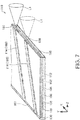
- Fig. 7 is a perspective view schematically showing a light emitting device of the illumination device according to the embodiment.
- Fig. 8 is a plan view schematically showing the light emitting device of the illumination device according to the embodiment.
- Fig. 9 is a sectional view schematically showing the light emitting device of the illumination device according to the embodiment.
- Fig. 10 schematically shows an illumination device according to a first modified example of the embodiment.
- Fig. 11 is a plan view schematically showing a light emitting device of an illumination device according to a second modified example of the embodiment.
- Fig. 12 schematically shows a light source of an illumination device according to a third modified example of the embodiment.
- Fig. 13 is a plan view schematically showing a light emitting device of the illumination device according to the third modified example of the embodiment.
- Fig. 14 is a plan view schematically showing the light emitting device of the illumination device according to the third modified example of the embodiment.
- Fig. 15 schematically shows a light source of an illumination device according to a fourth modified example of the embodiment.
- Fig. 16 schematically shows sectional shapes of light output from light distribution control devices of the illumination device according to the fourth modified example of the embodiment.
- Fig. 17 is a plan view schematically showing a light emitting device of an illumination device according to a fifth modified example of the embodiment.
- Fig. 18 is a plan view schematically showing a light emitting device of an illumination device according to a sixth modified example of the embodiment.
- Fig. 19 is a plan view schematically showing a light emitting device of an illumination device according to a seventh modified example of the embodiment.
- Fig. 20 schematically shows a projector according to an embodiment.
- Fig. 1 schematically shows an illumination device 100 according to the embodiment.
- Fig. 2 schematically shows a light source 10 of the illumination device 100 according to the embodiment as seen from an output surface 180 side, which will be described later. Note that, in Fig. 1 , for convenience, a light emitting device 110 forming the light source 10 will be simplified for ease of illustration.
- the illumination device 100 includes the light source 10, an optical axis conversion device 20, and a light distribution control device 30. Further, the illumination device 100 may include a diffusion device 40.
- the light source 10 may output light.
- the light source 10 may include the light emitting device 110 and a support substrate 12 as shown in Fig. 2 .
- a plurality of the light emitting devices 110 are provided, and they are arranged at equal intervals along the Y-axis direction. In the illustrated embodiment, six of the light emitting devices 110 are provided, however, the number is not particularly limited.
- Each light emitting device 110 has plural tilted gain regions 160 as shown in Fig. 1 . That is, the plural tilted gain regions 160 are formed on the same substrate. Thereby, the alignment of the light source 10 with the optical axis conversion device 20, the light distribution control device 30, and other embodiments becomes easier and control of the light distribution properties of the illumination light illuminating an illumination target 50 becomes easier.
- the plural tilted gain regions 160 are provided in parallel to one another, for example. In the example shown in Fig. 1 , six of the tilted gain regions 160 are provided, however, the number is not particularly limited.
- the tilted gain regions 160 are arranged at equal intervals along the X-axis direction, for example, in one light emitting device 110.
- Each tilted gain region 160 has an output surface 180 that outputs light.
- the output surfaces 180 are arranged at equal intervals Dx along the X-axis direction as shown in Fig. 2 .
- the light source 10 includes plural light emitting devices 110 arranged in the Y-axis direction as shown in Fig. 2 .
- the output surfaces 180 are arranged at equal intervals Dy along the Y-axis direction.
- Fig. 3 schematically shows an angular distribution of light L1 output from the light emitting device 110 (from the tilted gain region 160).
- the tilted gain region 160 is tilted with respect to the perpendicular of the output surface 180 as shown in Fig. 1 .
- the light L1 output from the tilted gain region 160 has an arched angular distribution similar to a crescent shape as shown in Fig. 3 .
- the light distribution angle in the X-axis direction is about ⁇ 10° and the light distribution angle in the Y-axis direction is about ⁇ 35°, and the angular distribution spreads greatly in the Y-axis direction as compared to that in the X-axis direction.
- the sectional shape of the luminous flux is also arched like a crescent (in the downstream position slightly spaced apart from the light emitting device 110) .
- the detailed configuration of the light emitting device 110 will be described later.
- Each support substrate 12 supports a light emitting device 110 as shown in Fig. 2 .
- a plurality of the support substrates 12 are provided for the light emitting devices 110.
- the material of the support substrate 12 is not particularly limited, and copper or aluminum may be used, for example.
- the light output from the light source 10 enters the optical axis conversion device 20.
- the optical axis of the light output from the light emitting device 110 is tilted to a greater extent than the tilt angle of the tilted gain region 160 (with respect to the perpendicular of the output surface 180) due to a difference in refractive index between the light emitting device 110 and the air. That is, the optical axis of the light output from the light emitting device 110 is tilted with respect to an illumination optical axis P (also referred to as "the perpendicular of the illuminated surface of the illumination target 50").
- the optical axis conversion device 20 may bring the optical axis of the light tilted with respect to the illumination optical axis P (nearly) in parallel to the illumination optical axis P. That is, the light output from the optical axis conversion device 20 may have an optical axis (nearly) in parallel to the illumination optical axis P.
- a prism having slopes 22 forming predetermined angles with respect to the illumination optical axis P arranged to correspond to the output surfaces 180 in an array may be used.
- the optical axis conversion device 20 has six slopes 22 corresponding to the six output surfaces 180.
- the slope 22 may be a flat surface.
- the tilt angle of the slope 22 with respect to the illumination optical axis P is determined by a refractive index of a material forming the prism and the tilt angle of the optical axis (with respect to the illumination optical axis P) of the light entering the optical axis conversion device 20.
- a holographic optical device may be used, or a combination of a prism and a holographic optical device may be used, for example.
- the light output from the optical axis conversion device 20 enters the light distribution control device 30.
- the light distribution control device 30 converts the angular distribution of the output light into predetermined values and the asymmetry in the angular distribution may be improved and brought closer to a symmetric angular distribution.
- Fig. 4 schematically shows an angular distribution of light L2 output from the light distribution control device 30 (showing output light from one light emitting device 110). As can be seen in Figs.
- the light distribution angle in the X-axis direction becomes narrower from about 110° before incidence to the light distribution control device 30 to about ⁇ 2° after incidence and the light distribution angle in the Y-axis direction becomes narrower from about ⁇ 35° before incidence to the light distribution control device 30 to about ⁇ 4° after incidence, and the asymmetry in the angular distribution is improved at the same time.
- the sectional shape of the light L2 output from the light distribution control device 30 becomes an oval shape with high symmetry from the arched shape similar to a crescent.
- the light output from the light distribution control device 30 enters the diffusion device 40.
- the diffusion device 40 diffuses the light output from the respective plural output surfaces 180, and thereby, may further improve the symmetry of the sectional shape of each light and make the light intensity distribution (illuminance distribution) of the entire illumination light on the illumination target 50 (nearly) uniform.
- a diffusion plate for example, a diffusion plate, a holographic optical device, a lens array, or a combination of these may be used.
- a diffusion plate is used as the diffusion device 40.
- Fig. 5 schematically shows a sectional shape of light L3 output from the diffusion device 40 (showing output light from one light emitting device 110), and Fig.
- FIG. 6 schematically shows an angular distribution of the light L3 output from the diffusion device 40.
- the sectional shape is an oval shape close to a circular shape, and the angular distribution has high symmetry close to a circular shape.
- a lens array including lenses 32 having collecting action in an array may be used as shown in Fig. 1 .
- the plural lenses 32 are provided to correspond to the output surfaces 180 of the light source 10.
- a spherical lens, an aspherical lens having an axis of symmetry, a toric lens having different radii of curvature in the X-axis direction and the Y-axis direction, a free-form surface lens having no axis of symmetry, a Fresnel lens having a discontinuous curved surface, or the like may be used.
- the radiation angles of light output from the light emitting device are often different in the X-axis direction and the Y-axis direction in Fig. 1 . Therefore, in the case where the aspherical lens, the toric lens, the free-form surface lens, or the like is used as the lens 32, the direction of the light output from the light distribution control device 30 may be independently controlled with respect to the X-axis direction and the Y-axis direction and the light distribution of the light L2 output from the light distribution control device 30 may be finely controlled, and thus, the sectional shape may be brought close to a circular shape having high symmetry. However, the spherical lens is easily employed in respect of costs.
- a holographic optical device may be used, or a combination of a prism and a holographic optical device may be used, for example.
- the light output from the respective plural output surfaces 180 may diverge to partially overlap at least with the light output from the adjacent output surfaces 180 on the illumination target 50. Therefore, for example, as compared to the case where the illumination target is illuminated by the light output from the adjacent plural output surfaces 180 but not partially overlapping with each other, the illumination target may be illuminated with uniform intensity (illuminance distribution) In the case of illumination using light not partially overlapping on the illumination target, the illumination intensity is significantly lower at the boundaries between adjacent light, and a non-uniform illuminance distribution is often formed.
- the light distribution angle of the light output from the diffusion device 40 (may be referred to as "tilt angle", or “diverging angle” with respect to the illumination optical axis P) is set to an angle at which the illumination target (the light modulation device for the projector) can receive light or an angle at which projection can be performed in the projection system (projection device).
- the light distribution angle (angular distribution range) of the light output from the diffusion device 40 is set in a range from more than 0° to equal to or less than 20°.
- the light output from the respective plural output surfaces 180 overlap with the light output from the next output surfaces 180 on the illumination target 50, however, the light may overlap with the light output from other output surfaces 180. For example from the output surfaces 180 next to the next. Note that the light output from the respective plural output surfaces 180 do not completely overlap. Therefore, by controlling light intensity of output light with respect to each tilted gain region 160, local regions on the illumination target 50 may be independently illuminated with arbitrary light intensity, Especially, in the case where a light modulation device such as a liquid crystal light valve is illuminated, light intensity modulation by the illumination device and light intensity modulation by the light modulation device are simultaneously performed, and thereby, both high brightness and high contrast may be realized and higher image quality of displayed images may be realized.
- a light modulation device such as a liquid crystal light valve
- overlapping of light A and light B on the illumination target means overlapping of illumination region of the light A and the illumination region of the light B on the illumination target, and the illumination regions of the light A and the light B mean regions having intensity equal to or more than 10o relative to the intensity at the center of the light.
- the optical axis conversion device 20 and the light distribution control device 30 are formed in contact with each other, however, they may be formed apart.
- the optical axis conversion device 20 and the light distribution control device 30 may be integrally formed.
- the optical axis conversion device 20 may be obtained by forming plural slopes 22 on one surface of one glass substrate and the light distribution control device 30 may be obtained by forming plural lenses 32 on the other surface (the opposite surface to the one surface) .
- the optical axis conversion device 20 may be obtained by forming plural slopes 22 on one surface of one glass substrate and the light distribution control device 30 may be obtained by forming plural lenses 32 on the other surface (the opposite surface to the one surface) .
- the diffusion device 40 is provided in a position apart from the light distribution control device 30, however, the device 40 may be integrated with the light distribution control device 30 for reduction of light loss at the interface.
- the diffusion device 40 may be formed on the surface of the lens array for integrated configuration.
- the light output from the diffusion device 40 illuminates the illumination target 50.
- the illumination target 50 although not particularly limited, a liquid crystal light valve (light modulation device) may be cited in the case where the illumination device 100 is used for a projector.
- Fig. 7 is a perspective view schematically showing the light emitting device 110 according to the embodiment.
- Fig. 8 is a plan view schematically showing the light emitting device 110 according to the embodiment.
- Fig. 9 is a sectional view schematically showing the light emitting device 110 according to the embodiment along IX-IX line in Fig. 8 . Note that, in Figs. 7 to 9 , for convenience, two tilted gain regions 160 are shown.
- the light emitting device 110 is an SLD that emits red light of an InGaAlP system.
- the SLD can prevent laser oscillation by suppressing the formation of a resonator due to edge reflection. Accordingly, speckle noise may be reduced.
- the light emitting device 110 includes a substrate 102, a first cladding layer 104, an active layer 106, a second cladding layer 108, a contact layer 109, a first electrode 112, a second electrode 114, and a reflection film 130.
- a first conductivity-type (for example, n-type) GaAs substrate or the like may be used.
- the first cladding layer 104 is formed on the substrate 102.
- As the first cladding layer 104 for example, an n-type InGaAlp layer or the like may be used.
- the active layer 106 is formed on the first cladding layer 104.
- the active layer 106 has a multiple quantum well (MQW) structure in which three quantum well structures each including an InGaP well layer and an InGaAlP barrier layer, for example, are stacked.
- MQW multiple quantum well
- the shape of the active layer 106 is a rectangular parallelepiped (including the case of a cube), for example.
- the active layer 106 may have a first side surface 105 and a second side surface 107 as shown in Figs. 7 and 8 .
- the first side surface 105 and the second side surface 107 are opposed to each other, and in parallel in the illustrated example.
- the tilted gain regions 160 may serve as current channels.
- the tilted gain region 160 may be generated and the light may be amplified within the tilted gain regions 160.
- the tilted gain region 160 may be referred to as "light propagation region (waveguide region)".
- the planar shape of the tilted gain region 160 seen from the stacking direction of the light emitting device 110 is a parallelogram, for example.
- reflectance of the second side surface 107 is higher than reflectance of the first side surface 105.
- the reflection film 130 is a dielectric multilayer mirror, for example.
- a mirror in which four pairs of an Al 2 O 3 layer and a TiO 2 layer are stacked from the second side surface 107 side in this order may be used. It is desirable that the reflectance of the second side surface 107 is just or nearly 100%.
- it is desirable that the reflectance of the first side surface 105 is just or nearly 0%.
- an antireflection film an Al 2 O 3 single layer may be used, for example.
- the tilted gain regions 160 are provided so that the extension direction from the first side surface 105 to the second side surface 107 (guiding direction of light) may be tilted with respect to a perpendicular line Q of the first side surface 105 in the plan view (seen from the Y-axis direction) as shown in Fig. 8 . Thereby, laser oscillation of the light generated in the tilted gain regions 160 may be suppressed or prevented. As shown in Figs. 1 and 8 , the plural tilted gain regions 160 are provided at tilts in the same direction with respect to the perpendicular line Q.
- the tilted gain region 160 may have a first end surface 180 provided on the first side surface 105 and a second end surface 182 provided on the second side surface 107 as shown in Fig. 8 . Accordingly, in the wavelength band of light generated in the tilted gain region 160, reflectance of the first end surface 180 is just or nearly 0%, for example, and reflectance of the second end surface 182 is just or nearly 100%, for example. Therefore, the first end surface 180 is an output surface that outputs light generated in the tilted gain region 160 (corresponding to the output surface 180 in Fig. 1 ), and the second end surface 182 is a reflection surface that reflects the light generated in the tilted gain region 160. That is, the first side surface 105 may have plural output surfaces 180 (first end surfaces 180) and the perpendicular line Q of the first side surface 105 is also the perpendicular line Q of the output surfaces 180.
- the second cladding layer 108 is formed on the active layer 106 as shown in Figs. 7 and 9 .
- a second conductivity-type (for example, p-type) AlGalnP layer or the like may be used as the second cladding layer 108.
- the p-type second cladding layer 108, the active layer 106 not doped with impurity, and the n-type first cladding layer 104 form a pin diode.
- Each of the first cladding layer 104 and the second cladding layer 108 is a layer having a larger forbidden band width and a lower refractive index than those of the active layer 106.
- the active layer 106 has a function of generating and guiding light and amplifying the light by injecting carriers (electrons and holes).
- the first cladding layer 104 and the second cladding layer 108 sandwich the active layer 106 and have a function of confining injected carriers (electrons and holes) and light.
- the light emitting device 110 when a forward bias voltage of the pin diode is applied between the first electrode 112 and the second electrode 114, recombination of electrons and holes occurs in the tilted gain region 160 of the active layer 106. Light is emitted by the recombination. Starting from the generated light, chained stimulated emission occurs and the intensity of the light is amplified within the tilted gain region 160. Then, the light with amplified intensity is output from the output surface 180 of the tilted gain region 160 as light L1 as shown in Fig. 7 .
- the contact layer 109 is formed on the second cladding layer 108 as shown in Figs. 7 and 9 .
- a layer in ohmic contact with the second electrode 114 may be used.
- a p-type GaAs layer may be used.
- the first electrode 112 is formed on the entire surface under the substrate 102.
- the first electrode 112 may be in contact with a layer (the substrate 102 in the illustrated example) in ohmic contact with the first electrode 112.
- the first electrode 112 is electrically connected to the first cladding layer 104 via the substrate 102.
- the first electrode 112 is one electrode for driving the light emitting device 110.
- an electrode formed by stacking a Cr layer, an AuGe layer, an Ni layer, and an Au layer in this order from the substrate 102 side may be used.
- the second electrode 114 is formed on the contact layer 109.
- the second electrode 114 is electrically connected to the second cladding layer 108 via the contact layer 109.
- the second electrode 114 is the other electrode for driving the light emitting device 110.
- As the second electrode 114 for example, an electrode formed by stacking a Cr layer, an AuZn layer, and an Au layer in this order from the contact layer 109 side may be used.
- the lower surface of the second electrode 114 (the contact surface between the second electrode 114 and the contact layer 109) may have the same planar shape as that of the tilted gain region 160.
- the planar shape of the contact surface between the second electrode 114 and the contact layer 109 current channels between the electrodes 112, 114 are determined and, as a result, the planar shape of the tilted gain region 160 may be determined.
- the light emitting device 110 may be of a refractive index-guiding type that confines light by patterning the contact layer 109 and the second cladding layer 108 to form columnar parts and providing refractive index differences between regions where the columnar parts are formed and regions the columnar parts are not formed may be used.
- any material system that can form an emission gain region may be used in the light emitting device 110.
- a semiconductor material for example, a semiconductor material of an AlGaN system, an InGaN system, a GaAs system, anAlGaAs system, an InGaAs system, an InGaAsP system, a ZnCdSe system, or the like may be used.
- the following characteristics are provided.
- the optical axis of the output light from the light emitting device 110 and the illumination optical axis P may be nearly aligned by the optical axis conversion device 20, and the light distribution angle (anglular distribution) of the illumination light may be controlled to a desired value by the light distribution control device 30 and the diffusion device 40.
- the light having the arched sectional shape like a crescent and the angular distribution with low symmetry generated by the tilted gain region 160 may be converted into light having a nearly circular sectional shape and an angular distribution with high symmetry. Therefore, the illumination device 100 may improve the symmetry of the illumination light that illuminates the illumination target 50.
- the light output from the light distribution control device 30 and the diffusion device 40 may diverge. Accordingly, the light output from the respective plural output surfaces 180 may partially overlap at least with the light output from the adjacent output surfaces 180 on the illumination target 50. Thereby, in the illumination device 100, for example, as compared to the case where the illumination target is illuminated by light that does not even partially overlap, the illumination target may be illuminated with uniform intensity (illuminance distribution).
- the diffusion device 40 has been provided, however, depending on the properties (the sectional shape and the angular distribution) of the output light from the light emitting device 110, illumination light having desired properties may be obtained without using the diffusion device 40, and instead only using the light distribution control device 30.
- FIG. 10 schematically shows an illumination device 200 according to the first modified example of the embodiment.
- the same reference signs are assigned to members having the same functions as those of the component members of the illumination device 100 according to the embodiment, and a detailed explanation will be omitted. This applies to illumination devices 300, 400, 500, 600 according to second to fifth modified examples of the embodiment, which will be described later.
- the illumination device 200 includes a light guide 60.
- the light guide 60 may guide light output from the diffusion device 40 to the illumination target 50
- the light guide 60 is provided between the diffusion device 40 and the illumination target 50.
- the light guide 60 for example, one having a mirror body formed on the inner surface of a tubular member, a rod-shaped light transmissive medium, or the like may be used.
- reflection surfaces 61 are provided except in a part that the light output from the diffusion device 40 enters and a part that outputs the light from the light guide 60 to the illumination target 50.
- the reflection surface 61 may include a mirror body or may be formed by a total reflection surface.
- the illumination efficiency may be improved without significant reduction of illumination uniformity.
- the sectional shape and the size (the shape and the size in the XY plane) of the light output edge of the light guide 60 are made nearly equal to the sectional shape and the size of the illumination target 50, however, the shape is not limited to these.
- dimensions and shapes in which the sectional shape of the light output part of the light guide 60 is a similar shape with respect to the sectional shape of the illumination target 50 and the size of the light output part of the light guide 60 is slightly larger than the size of the illumination target 50 or slightly smaller or the like may be employed. That is, it is desirable that the sectional shape and the size of the light output edge of the light guide 60 are set in consideration of the light distribution angle (diverging angle) of the illumination light so that the illumination target 50 may be illuminated (nearly) uniformly.
- Fig. 1 is a plan view schematically showing a light emitting device 110 of an illumination device 300 according to the second modified example of the embodiment.
- Fig. 11 for convenience, the light emitting device 110 is simplified for illustration.
- the plural tilted gain regions 160 of the light emitting device 110 have been tilted toward the same side with respect to the perpendicular Q of the first side surface 105.
- first tilted gain regions 160a of the plural tilted gain regions 160 are tilted toward one side with respect to the perpendicular Q and second tilted gain regions 160b of the plural tilted gain regions 160 are tilted toward the other side (different from the one side) with respect to the perpendicular Q.
- the first tilted gain regions 160a and the second tilted gain regions 160b may have shapes symmetric with respect to the perpendicular Q.
- the first tilted gain regions 160a and the second tilted gain regions 160b are provided in the same number and alternately arranged along the X-axis direction.
- the light L2 output from the light distribution control device 30 has improved symmetry in the angular distribution (symmetry of the sectional shape of light) as shown in Fig. 4 , however, the sectional shape of the light L2 may not be completely formed in an oval shape. Accordingly, in the illumination device 300, as shown in Fig. 11 , by changing the tilt directions of the plural tilted gain regions 160 and providing them as the first tilted gain regions 160a and the second tilted gain regions 160b, the symmetry in the angular distribution seen as the entire illumination light may be further improved.
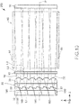
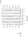
- FIG. 12 schematically shows the light source 10 of an illumination device 400 according to the third modified example of the embodiment corresponding to Fig. 2 .
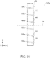
- Figs. 13 and 14 are plan views schematically showing the light emitting device 110 of the illumination device 400 according to the third modified example of the embodiment. Note that, in Figs. 13 and 14 , for convenience, the light emitting device 110 is simplified for illustration.
- first light emitting devices 110a and second light emitting devices 110b of the plural light emitting devices 110 are alternately arranged along the Y-axis direction.
- the first light emitting devices 110a and the second light emitting devices 110b are provided in the same number.
- the plural tilted gain regions 160 are the first tilted gain regions 160a tilted toward one side with respect to the perpendicular Q of the first side surface 105.
- the plural tilted gain regions 160 are the second tilted gain regions 160b tilted toward the other side (different from the one side) with respect to the perpendicular Q.
- the number of first tilted gain regions 160a provided in the first light emitting device 110a and the number of second tilted gain regions 160b provided in the second light emitting device 110b are the same.
- the symmetry in the angular distribution seen as the entire illumination light may be further improved as compared to the example of the illumination device 100.
- FIG. 15 schematically shows the light source 10 of an illumination device 500 according to the fourth modified example of the embodiment corresponding to Fig. 2 .
- the output surfaces 180 of the light source 10 are arranged in a matrix at equal intervals in the XY plane.
- the plural output surfaces 180 are arranged so that the distance Dy between the adjacent output surfaces 180 in the Y-axis direction is larger than the distance Dx between the adjacent output surfaces 180 in the X-axis direction.
- the light L2 output from the light distribution control device 30 has improved symmetry in the angular distribution as shown in Fig. 4 , however, the angular distribution is often different between the X-axis direction and the Y-axis direction. Accordingly, if the output surfaces 180 are arranged in the XY plane at equal intervals, the illuminance distribution of illumination light may not be uniform in the X-axis direction and the Y-axis direction. For example, in the example shown in Fig.
- the Y-axis direction is the stacking direction of the light emitting device 110
- the confinement width of light within the light emitting device 110 in the Y-axis direction is smaller than the confinement width of light in the X-axis direction. Therefore, regarding the light L2, the light distribution angle in the Y-axis direction is larger than the light distribution angle in the X-axis direction.
- the plural lights L2 may be made closer in the X-axis direction and the Y-axis direction.
- the degree of overlapping may be made closer in the X-axis direction and the Y-axis direction.
- the uniformity of the illuminance distribution of illumination light on the illumination target may be improved.
- FIG. 16 the sectional shapes of the light L2 output from the plural light distribution control devices 30 are schematically shown and the sectional shapes of the light L2 are illustrated as oval shapes for convenience.
- FIG. 17 is a plan view schematically showing the light emitting device 110 of an illumination device 600 according to the fifth modified example of the embodiment corresponding to Fig. 8 .
- a pair of gain regions 163 including a first gain region 161 and a second gain region 162 is used as the tilted gain region 160.
- plural pairs of gain regions 163 are provided and arranged along the X-axis direction.
- the first gain region 161 is tilted toward one side with respect to the perpendicular Q of the first side surface 105 and provided from the first side surface 105 to the second side surface 107.
- the second gain region 162 is tilted toward the other side (different from the one side) with respect to the perpendicular Q and provided from the first side surface 105 to the second side surface 107.
- the first gain region 161 and the second gain region 162 are provided symmetrically with respect to the perpendicular Q.
- a first end surface 180 (output surface 180) of the first gain region 161 and a first end surface 180 of the second gain region 162 are separated from each other.
- a second end surface 182 (reflection surface 182) of the first gain region 161 and a second end surface 182 of the second gain region 162 overlap at least partially on the second side surface 107, and completely overlap in the illustrated example. That is, the pair of gain regions 163 may have a planar shape of a V shape seen from the stacking direction of the light emitting device 110.
- part of the light generated in the first gain region 161 is reflected on the second side surface 107 (second end surface 182) and output from the first end surface 180 of the second gain region 162, and its light intensity is amplified in the meantime.
- part of the light generated in the second gain region 162 is reflected on the second side surface 107 and output from the first end surface 180 of the first gain region 161, and its light intensity is amplified in the meantime.
- the light generated in the first gain region 161 may include light directly output from the first end surface 180 of the first gain region 161.
- the light generated in the second gain region 162 may include light directly output from the first end surface 180 of the second gain region 162.
- the symmetry in the angular distribution seen as the entire illumination light may be further improved as compared to the example of the illumination device 100.
- Fig. 18 is a plan view schematically showing the light emitting device 110 of an illumination device 700 according to the sixth modified example of the embodiment corresponding to Fig. 17 .
- the same reference signs are assigned to members having the same functions as the component members of the illumination device 600 according to the fifth modified example of the embodiment, and their detailed explanation will be omitted.
- the light emitting device 110 of the illumination device 700 has a reflection part 140 as shown in Fig. 18 .
- the reflection part 140 is provided inside of an outer periphery of the active layer 106 in a plan view (seen from the Y-axis direction).
- a DBR (Distributed Bragg Reflector) mirror including plural grooves 142 arranged at predetermined intervals may be used.
- the interior of the groove 142 may be hollow (air) or filled with an insulating member. In the illustrated example, four of the grooves 142 are provided, however, the number of grooves is not limited thereto.
- the reflection part 140 may reflect the light generated in the first gain region 161 and the second gain region 162.
- the second gain region 162 includes a first part 162a and a second part 162b.
- the first part 162a is provided from the first side surface 105 to the reflection part 140.
- the first part 162a may have a first end surface 180.
- the first part 162a is parallel to the first gain region 161, for example.
- the second part 162b is provided from the reflection part 140 to the second side surface 107.
- the second part 162b may have a second end surface 182.
- the first part 162a and the second part 162b overlap in the reflection part 140.
- the first part 162a and the second part 162b are provided symmetrically with respect to an imaginary line R orthogonal to the perpendicular Q of the first side surface 105.
- part of light generated in the first gain region 161 is reflected on the second side surface 107 and the reflection part 140 and output from the first end surface 180 of the second gain region 162 (first part 162a) .
- the optical axis of the light output from the first end surface 180 of the first gain region 161 and the optical axis of the light output from the first end surface 180 of the second gain region 162 may be made (nearly) in parallel. Accordingly, in the illumination device 700, for example, the design of the optical system including the optical axis conversion device 20 may be simplified as compared to the illumination device 600.
- FIG. 19 is a plan view schematically showing the light emitting device 110 of an illumination device 800 according to the seventh modified example of the embodiment corresponding to Fig. 18 .
- the same reference signs are assigned to members having the same functions as the component members of the illumination device 700 according to the sixth modified example of the embodiment, and their detailed explanation will be omitted.
- the light emitting device 110 of the illumination device 800 does not have the reflection part 140 unlike the light emitting device 110 of the illumination device 700 as shown in Fig. 19 , however, the optical axis of the light output from the first end surface 180 of the first gain region 161 and the optical axis of the light output from the first end surface 180 of the second gain region 162 may be made (nearly) in parallel.
- the second gain region 162 has a third part 162c having a planar shape of an arc (or an oval arc).
- the third part 162c is provided between the first part 162a and the second part 162b of the second gain region 162 . More specifically, the first part 162a is linearly extended from the first side surface 105 and connected to the third part 162c. Further, the second part 162b is linearly extended from the second side surface 107 and connected to the third part 162c.
- part of the light generated in the first gain region 161 is reflected on the second side surface 107, and then, while traveling within the third part 162c, the traveling direction is bent and output from the first end surface 180 of the first part 162a. Accordingly, as described above, in the illumination device 800, the optical axis of the light output from the first end surface 180 of the first gain region 161 and the optical axis of the light output from the first end surface 180 of the second gain region 162 may be made (nearly) in parallel.
- FIG. 20 schematically shows a projector 900 according to the embodiment. Note that, in Fig. 20 , for convenience, a casing of the projector 900 is omitted for illustration.
- the projector 900 may include a red illumination device that outputs red light, a green illumination device that outputs green light, and a blue illumination device that outputs blue light.
- the illumination devices according to the invention may be used. As shown in Fig. 20 , an example using the illumination device 100 (the red illumination device 100R, the green illumination device 100G, the blue illumination device 100B) as the illumination device of the projector 900 will be explained.
- the projector 900 further includes transmissive liquid crystal light valves (light modulation devices) 950R, 950G, 950B, a cross dichroic prism (color light combining means) 970, and a projection lens (projection device) 980.
- transmissive liquid crystal light valves light modulation devices
- 950R, 950G, 950B transmissive liquid crystal light valves
- a cross dichroic prism color light combining means
- projection lens projection device
- the light output from the respective illumination devices 100R, 100G, 100B enter the respective liquid crystal light valves 950R, 950G, 950B.
- the respective liquid crystal light valves 950R, 950G, 950B respectively modulate incident light in response to image information. Note that the liquid crystal light valves 950R, 950G, 950B correspond to the illumination target 50 shown in Fig. 1 .
- the cross dichroic prism 970 is formed by bonding four right angle prisms, for example, and a dielectric multilayer film that reflects red light and a dielectric multilayer film that reflects blue light are provided crosswise on its inner surface. By the dielectric multilayer films, the three colors of light are combined and light representing a color image is formed.
- the light combined by the cross dichroic prism 970 enters the projection lens 980 as a projection system.
- the projection lens 980 enlarges the images formed by the liquid crystal light valves 950R, 950G, 950B and projects them on a screen (display surface) 990.
- the light distribution angles (angular distributions) of the light output from the illumination devices 100R, 100G, 100B are set to be projectable angles in the projection lens 980. More specifically, the light distribution angles of the light output from the illumination devices 100R, 100G, 100B are set to be equal to or less than about 20°.
- the transmissive liquid crystal light valves have been used as light modulation devices, however, other light valves may be used, or reflective light valves may be used.
- the light valves for example, reflective liquid crystal light valves and digital micromirror devices are cited.
- the configuration of the projection system may be appropriately changed depending on the type of light valves.
- the illumination device according to the invention may be included.
- the liquid crystal light valves light modulation devices
- the illumination device 100 may be uniformly illuminated by illumination light with high symmetry, but without illuminance irregularities. Accordingly, in the projector 900, higher image quality (higher brightness and higher contrast) of the projection image may be realized.
Landscapes
- Physics & Mathematics (AREA)
- General Physics & Mathematics (AREA)
- Optics & Photonics (AREA)
- Projection Apparatus (AREA)
- Non-Portable Lighting Devices Or Systems Thereof (AREA)
- Optical Elements Other Than Lenses (AREA)
Abstract
Description
- The present invention relates to an illumination device and a projector.
- The development of projectors using an array of light sources with plural semiconductor light emitting devices is being advanced. Known semiconductor light emitting devices include, for example, a semiconductor laser (laser diode), a super luminescent diode (hereinafter, may be referred to as "SLD"), an LED (light emitting diode), and an OLED (organic light emitting diode).
- Among these devices, the SLD has a slight disadvantage with respect to light output, but has the advantage of an inherently smaller speckle noise due to the presence of a different gain region structure as compared to a semiconductor laser. However, due to a nonresonant structure in which the gain region is provided at a tilt with respect to an end surface (output surface) of a substrate with the semiconductor light emitting device formed thereon, the output light has an angular distribution with low symmetry similar to a crescent shape.
- Generally, many light modulation devices used for projectors have display properties dependent on the incident angles of incident illumination light. Accordingly, to realize a projection image with high image quality, it is desirable to use illumination light having high angular distribution symmetry (which may be referred to as "symmetry of sectional shape of light") and a uniform intensity distribution. This is because angular distribution asymmetry and the intensity distribution nonuniformity cause brightness irregularities and contrast irregularities.
- For example, Patent Document 1 (International Publication
WO 99/49358 - However, in the configuration of
Patent Document 1, if the semiconductor lasers are simply replaced with SLDs, the angular distributions of the output light are very different due to the difference in the gain region structure between the semiconductor lasers and the SLDs as described above, and thus r it is difficult to obtain a desired illumination condition. - An advantage of some aspects of the invention is to provide an illumination device that may improve the symmetry of illumination light in a light source using SLDs. Another advantage of some aspects of the invention is to provide a projector having the illumination device.
- An illumination device according to an aspect of the invention includes a light source including plural light emitting devices that generate and guide light and have tilted gain regions in which guiding directions of the light are tilted with respect to a perpendicular of output surfaces of the light, an optical axis conversion device that bends optical axes of the light output from the light source, and a light distribution control device that controls a light distribution angle of the light output from the optical axis conversion device, wherein the light emitting devices are super luminescent diodes, and the light output from the light distribution control device diverge.
- According to the illumination device, the light distribution angle of the light output from the optical axis conversion device may be controlled by the light distribution control device. Thereby, the light having an arched sectional shape like a crescent and an angular distribution with low symmetry generated by the tilted gain region may be converted into light having a nearly oval sectional shape and an angular distribution with high symmetry. Therefore, the symmetry of the illumination light that illuminates an illumination target may be improved.
- Further, the light output from the light distribution control device may diverge. Accordingly, the light output from the respective plural output surfaces may partially overlap at least with the light output from the adjacent output surfaces on the illumination target. Thereby, for example, as compared to the case where the illumination target is illuminated by light output from the adjacent output surfaces that does not even partially overlap with each other, the illumination target may be illuminated with uniform intensity (illuminance distribution).
- The illumination device according to the aspect of the invention may further include a diffusion device that diffuses the light output from the light distribution control device.
- According to such an illumination device, intensity distributions of the light output from the respective output surfaces may be made (nearly) uniform, and illumination light with less illuminance irregularities may be obtained.
- The illumination device according to the aspect of the invention may further include a light guide that guides the light output from the diffusion device to the illumination target.
- According to such an illumination device, more light may illuminate the illumination target. Accordingly, the illumination efficiency may be improved without significant reduction of illumination uniformity.
- In the illumination device according to the aspect of the invention, the optical axis conversion device and the light distribution control device may be integrally formed.
- According to such an illumination device, light loss at the interface between the optical axis conversion device and the light distribution control device may be reduced. Further, the cost may be reduced.
- In the illumination device according to the aspect of the invention, the light emitting device may have a plurality of the tilted gain regions, the guiding direction of the light of a first tilted gain region of the plurality of the tilted gain regions may be tilted to one side with respect to the perpendicular line of the output surface, and the guiding direction of the light of a second tilted gain region of the plurality of the tilted gain regions may be tilted to the other side with respect to the perpendicular of the output surface.
- According to such an illumination device, the symmetry seen as the entire illumination light may be further improved.
- In the illumination device according to the aspect of the invention, the light source may include a first light emitting device having a first tilted gain region in which the guiding direction of the light is tilted to one side with respect to the perpendicular of the output surface, and a second light emitting device having a second tilted gain region in which the guiding direction of the light is tilted to the other side with respect to the perpendicular of the output surface.
- According to such an illumination device, the symmetry seen as the entire illumination light may be further improved.
- A projector according to another aspect of the invention includes an illumination device, a light modulation device that modulates light output from the illumination device in response to image information, and a projection device that projects an image formed by the light modulation device, and the illumination device includes a light source including arranged plural light emitting devices that generate and guide light and having tilted gain regions in which guiding directions of the light are tilted with respect to a perpendicular of output surfaces of the light, an optical axis conversion device that bends optical axes of the light output from the light source, and a light distribution control device that controls a light distribution angle of the light output from the optical axis conversion device, wherein the light emitting devices are super luminescent diodes, and the light output from the light distribution control device diverge.
- According to the projector, since the illumination device having high symmetry of illumination light is provided, higher image quality of a projection image may be realized.
- In the projector according to the aspect of the invention, a light distribution angle of the light controlled by the light distribution control device may be an angle projectable by the projection device.
- According to such a projector, since the illumination device according to the aspect of the invention is provided, higher image quality of a projection image may be realized.
- The invention will be described with reference to the accompanying drawings, wherein like numbers reference like elements.
-
Fig. 1 schematically shows an illumination device according to an embodiment. -
Fig. 2 schematically shows a light source of the illumination device according to the embodiment. -
Fig. 3 schematically shows an angular distribution of light output from the light source of the illumination device according to the embodiment. -
Fig. 4 schematically shows an angular distribution of light output from a light distribution control device of the illumination device according to the embodiment. -
Fig. 5 schematically shows a sectional shape of light output from a diffusion device of the illumination device according to the embodiment. -
Fig. 6 schematically shows an angular distribution of the light output from the diffusion device of the illumination device according to the embodiment. -
Fig. 7 is a perspective view schematically showing a light emitting device of the illumination device according to the embodiment. -
Fig. 8 is a plan view schematically showing the light emitting device of the illumination device according to the embodiment. -
Fig. 9 is a sectional view schematically showing the light emitting device of the illumination device according to the embodiment. -
Fig. 10 schematically shows an illumination device according to a first modified example of the embodiment. -
Fig. 11 is a plan view schematically showing a light emitting device of an illumination device according to a second modified example of the embodiment. -
Fig. 12 schematically shows a light source of an illumination device according to a third modified example of the embodiment. -
Fig. 13 is a plan view schematically showing a light emitting device of the illumination device according to the third modified example of the embodiment. -
Fig. 14 is a plan view schematically showing the light emitting device of the illumination device according to the third modified example of the embodiment. -
Fig. 15 schematically shows a light source of an illumination device according to a fourth modified example of the embodiment. -
Fig. 16 schematically shows sectional shapes of light output from light distribution control devices of the illumination device according to the fourth modified example of the embodiment. -
Fig. 17 is a plan view schematically showing a light emitting device of an illumination device according to a fifth modified example of the embodiment. -
Fig. 18 is a plan view schematically showing a light emitting device of an illumination device according to a sixth modified example of the embodiment. -
Fig. 19 is a plan view schematically showing a light emitting device of an illumination device according to a seventh modified example of the embodiment. -
Fig. 20 schematically shows a projector according to an embodiment. - A preferred embodiment of the invention will be explained below with reference to the drawings.
- First, a light emitting device according to an embodiment will be explained with reference to the drawings.
Fig. 1 schematically shows anillumination device 100 according to the embodiment.Fig. 2 schematically shows alight source 10 of theillumination device 100 according to the embodiment as seen from anoutput surface 180 side, which will be described later. Note that, inFig. 1 , for convenience, alight emitting device 110 forming thelight source 10 will be simplified for ease of illustration. - As shown in
Fig. 1 , theillumination device 100 includes thelight source 10, an opticalaxis conversion device 20, and a lightdistribution control device 30. Further, theillumination device 100 may include adiffusion device 40. - The
light source 10 may output light. Thelight source 10 may include thelight emitting device 110 and asupport substrate 12 as shown inFig. 2 . - As shown in
Fig. 2 , a plurality of thelight emitting devices 110 are provided, and they are arranged at equal intervals along the Y-axis direction. In the illustrated embodiment, six of thelight emitting devices 110 are provided, however, the number is not particularly limited. - Each
light emitting device 110 has plural tiltedgain regions 160 as shown inFig. 1 . That is, the plural tiltedgain regions 160 are formed on the same substrate. Thereby, the alignment of thelight source 10 with the opticalaxis conversion device 20, the lightdistribution control device 30, and other embodiments becomes easier and control of the light distribution properties of the illumination light illuminating anillumination target 50 becomes easier. The plural tiltedgain regions 160 are provided in parallel to one another, for example. In the example shown inFig. 1 , six of the tiltedgain regions 160 are provided, however, the number is not particularly limited. The tiltedgain regions 160 are arranged at equal intervals along the X-axis direction, for example, in onelight emitting device 110. Each tiltedgain region 160 has anoutput surface 180 that outputs light. The output surfaces 180 are arranged at equal intervals Dx along the X-axis direction as shown inFig. 2 . - As Stated above, the
light source 10 includes plurallight emitting devices 110 arranged in the Y-axis direction as shown inFig. 2 . The output surfaces 180 are arranged at equal intervals Dy along the Y-axis direction. For example, in the example shown inFig. 2 , the output surfaces 180 are arranged at equal intervals (Dx = Dy) in a matrix (in a two-dimensional array) in the XY plane. -
Fig. 3 schematically shows an angular distribution of light L1 output from the light emitting device 110 (from the tilted gain region 160). The tiltedgain region 160 is tilted with respect to the perpendicular of theoutput surface 180 as shown inFig. 1 . Accordingly, the light L1 output from the tiltedgain region 160 has an arched angular distribution similar to a crescent shape as shown inFig. 3 . In the illustrated example, the light distribution angle in the X-axis direction is about ±10° and the light distribution angle in the Y-axis direction is about ±35°, and the angular distribution spreads greatly in the Y-axis direction as compared to that in the X-axis direction. As described above, since the angular distribution of the light L1 output from thelight emitting device 110 has an arched shape like a crescent, the sectional shape of the luminous flux is also arched like a crescent (in the downstream position slightly spaced apart from the light emitting device 110) . The detailed configuration of thelight emitting device 110 will be described later. - Each
support substrate 12 supports alight emitting device 110 as shown inFig. 2 . A plurality of thesupport substrates 12 are provided for thelight emitting devices 110. The material of thesupport substrate 12 is not particularly limited, and copper or aluminum may be used, for example. - As shown in
Fig. 1 , the light output from thelight source 10 enters the opticalaxis conversion device 20. The optical axis of the light output from thelight emitting device 110 is tilted to a greater extent than the tilt angle of the tilted gain region 160 (with respect to the perpendicular of the output surface 180) due to a difference in refractive index between the light emittingdevice 110 and the air. That is, the optical axis of the light output from thelight emitting device 110 is tilted with respect to an illumination optical axis P (also referred to as "the perpendicular of the illuminated surface of theillumination target 50"). The opticalaxis conversion device 20 may bring the optical axis of the light tilted with respect to the illumination optical axis P (nearly) in parallel to the illumination optical axis P. That is, the light output from the opticalaxis conversion device 20 may have an optical axis (nearly) in parallel to the illumination optical axis P. - As the optical
axis conversion device 20, aprism having slopes 22 forming predetermined angles with respect to the illumination optical axis P arranged to correspond to the output surfaces 180 in an array may be used. In the illustrated example, the opticalaxis conversion device 20 has sixslopes 22 corresponding to the six output surfaces 180. Theslope 22 may be a flat surface. The tilt angle of theslope 22 with respect to the illumination optical axis P is determined by a refractive index of a material forming the prism and the tilt angle of the optical axis (with respect to the illumination optical axis P) of the light entering the opticalaxis conversion device 20. - Note that, as the optical
axis conversion device 20, a holographic optical device may be used, or a combination of a prism and a holographic optical device may be used, for example. - The light output from the optical
axis conversion device 20 enters the lightdistribution control device 30. The lightdistribution control device 30 converts the angular distribution of the output light into predetermined values and the asymmetry in the angular distribution may be improved and brought closer to a symmetric angular distribution.Fig. 4 schematically shows an angular distribution of light L2 output from the light distribution control device 30 (showing output light from one light emitting device 110). As can be seen inFigs. 3 and 4 , for example, the light distribution angle in the X-axis direction becomes narrower from about 110° before incidence to the lightdistribution control device 30 to about ±2° after incidence and the light distribution angle in the Y-axis direction becomes narrower from about ±35° before incidence to the lightdistribution control device 30 to about ±4° after incidence, and the asymmetry in the angular distribution is improved at the same time. As a result of the improvement of the asymmetry in the angular distribution, the sectional shape of the light L2 output from the lightdistribution control device 30 becomes an oval shape with high symmetry from the arched shape similar to a crescent. - The light output from the light
distribution control device 30 enters thediffusion device 40. Thediffusion device 40 diffuses the light output from the respective plural output surfaces 180, and thereby, may further improve the symmetry of the sectional shape of each light and make the light intensity distribution (illuminance distribution) of the entire illumination light on the illumination target 50 (nearly) uniform. As thediffusion device 40, for example, a diffusion plate, a holographic optical device, a lens array, or a combination of these may be used. In the illustrated example, a diffusion plate is used as thediffusion device 40.Fig. 5 schematically shows a sectional shape of light L3 output from the diffusion device 40 (showing output light from one light emitting device 110), andFig. 6 schematically shows an angular distribution of the light L3 output from thediffusion device 40. As can be seen inFigs. 5 and 6 , the sectional shape is an oval shape close to a circular shape, and the angular distribution has high symmetry close to a circular shape. - As the light
distribution control device 30, a lensarray including lenses 32 having collecting action in an array may be used as shown inFig. 1 . In the illustrated example, theplural lenses 32 are provided to correspond to the output surfaces 180 of thelight source 10. As thelens 32, a spherical lens, an aspherical lens having an axis of symmetry, a toric lens having different radii of curvature in the X-axis direction and the Y-axis direction, a free-form surface lens having no axis of symmetry, a Fresnel lens having a discontinuous curved surface, or the like may be used. In the case of the SLD, the radiation angles of light output from the light emitting device are often different in the X-axis direction and the Y-axis direction inFig. 1 . Therefore, in the case where the aspherical lens, the toric lens, the free-form surface lens, or the like is used as thelens 32, the direction of the light output from the lightdistribution control device 30 may be independently controlled with respect to the X-axis direction and the Y-axis direction and the light distribution of the light L2 output from the lightdistribution control device 30 may be finely controlled, and thus, the sectional shape may be brought close to a circular shape having high symmetry. However, the spherical lens is easily employed in respect of costs. - Note that, as the light
distribution control device 30, a holographic optical device may be used, or a combination of a prism and a holographic optical device may be used, for example. - As shown in
Fig. 1 , with the lightdistribution control device 30 and thediffusion device 40, the light output from the respective plural output surfaces 180 may diverge to partially overlap at least with the light output from the adjacent output surfaces 180 on theillumination target 50. Therefore, for example, as compared to the case where the illumination target is illuminated by the light output from the adjacent plural output surfaces 180 but not partially overlapping with each other, the illumination target may be illuminated with uniform intensity (illuminance distribution) In the case of illumination using light not partially overlapping on the illumination target, the illumination intensity is significantly lower at the boundaries between adjacent light, and a non-uniform illuminance distribution is often formed. - In the case where the
illumination device 100 is used for a projector, the light distribution angle of the light output from the diffusion device 40 (may be referred to as "tilt angle", or "diverging angle" with respect to the illumination optical axis P) is set to an angle at which the illumination target (the light modulation device for the projector) can receive light or an angle at which projection can be performed in the projection system (projection device). In the case of a typical projector, given that the maximum reception angle of the light modulation device and the maximum projectable angle are about 20°, it is desirable that the light distribution angle (angular distribution range) of the light output from thediffusion device 40 is set in a range from more than 0° to equal to or less than 20°. - In the illustrated example, the light output from the respective plural output surfaces 180 overlap with the light output from the next output surfaces 180 on the
illumination target 50, however, the light may overlap with the light output from other output surfaces 180. For example from the output surfaces 180 next to the next. Note that the light output from the respective plural output surfaces 180 do not completely overlap. Therefore, by controlling light intensity of output light with respect to each tiltedgain region 160, local regions on theillumination target 50 may be independently illuminated with arbitrary light intensity, Especially, in the case where a light modulation device such as a liquid crystal light valve is illuminated, light intensity modulation by the illumination device and light intensity modulation by the light modulation device are simultaneously performed, and thereby, both high brightness and high contrast may be realized and higher image quality of displayed images may be realized. - Note that, in the description of the embodiment of the invention, for example, overlapping of light A and light B on the illumination target means overlapping of illumination region of the light A and the illumination region of the light B on the illumination target, and the illumination regions of the light A and the light B mean regions having intensity equal to or more than 10o relative to the intensity at the center of the light.
- In the example shown in
Fig. 1 , the opticalaxis conversion device 20 and the lightdistribution control device 30 are formed in contact with each other, however, they may be formed apart. Alternatively, the opticalaxis conversion device 20 and the lightdistribution control device 30 may be integrally formed. For example, the opticalaxis conversion device 20 may be obtained by formingplural slopes 22 on one surface of one glass substrate and the lightdistribution control device 30 may be obtained by formingplural lenses 32 on the other surface (the opposite surface to the one surface) . Thereby, light loss at the interface between the opticalaxis conversion device 20 and the lightdistribution control device 30 may be reduced. Further, the cost may be reduced. - The
diffusion device 40 is provided in a position apart from the lightdistribution control device 30, however, thedevice 40 may be integrated with the lightdistribution control device 30 for reduction of light loss at the interface. For example, in the case where the lightdistribution control device 30 includes a lens array, thediffusion device 40 may be formed on the surface of the lens array for integrated configuration. - The light output from the
diffusion device 40 illuminates theillumination target 50. As theillumination target 50, although not particularly limited, a liquid crystal light valve (light modulation device) may be cited in the case where theillumination device 100 is used for a projector. - Next, the detailed configuration of the
light emitting device 110 will be explained.Fig. 7 is a perspective view schematically showing thelight emitting device 110 according to the embodiment.Fig. 8 is a plan view schematically showing thelight emitting device 110 according to the embodiment.Fig. 9 is a sectional view schematically showing thelight emitting device 110 according to the embodiment along IX-IX line inFig. 8 . Note that, inFigs. 7 to 9 , for convenience, two tiltedgain regions 160 are shown. - Below, a case where the
light emitting device 110 is an SLD that emits red light of an InGaAlP system will be explained. Unlike a semiconductor laser, the SLD can prevent laser oscillation by suppressing the formation of a resonator due to edge reflection. Accordingly, speckle noise may be reduced. - As shown in
Figs. 7 to 9 , thelight emitting device 110 includes asubstrate 102, afirst cladding layer 104, anactive layer 106, asecond cladding layer 108, acontact layer 109, afirst electrode 112, asecond electrode 114, and areflection film 130. - As the
substrate 102, for example, a first conductivity-type (for example, n-type) GaAs substrate or the like may be used. - The
first cladding layer 104 is formed on thesubstrate 102. As thefirst cladding layer 104, for example, an n-type InGaAlp layer or the like may be used. - The
active layer 106 is formed on thefirst cladding layer 104. Theactive layer 106 has a multiple quantum well (MQW) structure in which three quantum well structures each including an InGaP well layer and an InGaAlP barrier layer, for example, are stacked. - The shape of the
active layer 106 is a rectangular parallelepiped (including the case of a cube), for example. Theactive layer 106 may have afirst side surface 105 and asecond side surface 107 as shown inFigs. 7 and8 . Thefirst side surface 105 and thesecond side surface 107 are opposed to each other, and in parallel in the illustrated example. - Parts of the
active layer 106 form the tiltedgain regions 160 that may serve as current channels. In the tiltedgain region 160, light may be generated and the light may be amplified within the tiltedgain regions 160. The tiltedgain region 160 may be referred to as "light propagation region (waveguide region)". The planar shape of the tiltedgain region 160 seen from the stacking direction of thelight emitting device 110 is a parallelogram, for example. - In a wavelength band of light generated in the tilted
gain region 160, for example, reflectance of thesecond side surface 107 is higher than reflectance of thefirst side surface 105. For example, by covering thesecond side surface 107 with thereflection film 130, higher reflectance may be obtained. Thereflection film 130 is a dielectric multilayer mirror, for example. Specifically, as thereflection film 130, a mirror in which four pairs of an Al2O3 layer and a TiO2 layer are stacked from thesecond side surface 107 side in this order may be used. It is desirable that the reflectance of thesecond side surface 107 is just or nearly 100%. On the other hand, it is desirable that the reflectance of thefirst side surface 105 is just or nearly 0%. For example, by covering thefirst side surface 105 with an antireflection film (not shown), lower reflectance may be obtained. As the antireflection film, an Al2O3 single layer may be used, for example. - The tilted
gain regions 160 are provided so that the extension direction from thefirst side surface 105 to the second side surface 107 (guiding direction of light) may be tilted with respect to a perpendicular line Q of thefirst side surface 105 in the plan view (seen from the Y-axis direction) as shown inFig. 8 . Thereby, laser oscillation of the light generated in the tiltedgain regions 160 may be suppressed or prevented. As shown inFigs. 1 and8 , the plural tiltedgain regions 160 are provided at tilts in the same direction with respect to the perpendicular line Q. - The tilted
gain region 160 may have afirst end surface 180 provided on thefirst side surface 105 and asecond end surface 182 provided on thesecond side surface 107 as shown inFig. 8 . Accordingly, in the wavelength band of light generated in the tiltedgain region 160, reflectance of thefirst end surface 180 is just or nearly 0%, for example, and reflectance of thesecond end surface 182 is just or nearly 100%, for example. Therefore, thefirst end surface 180 is an output surface that outputs light generated in the tilted gain region 160 (corresponding to theoutput surface 180 inFig. 1 ), and thesecond end surface 182 is a reflection surface that reflects the light generated in the tiltedgain region 160. That is, thefirst side surface 105 may have plural output surfaces 180 (first end surfaces 180) and the perpendicular line Q of thefirst side surface 105 is also the perpendicular line Q of the output surfaces 180. - The
second cladding layer 108 is formed on theactive layer 106 as shown inFigs. 7 and9 . As thesecond cladding layer 108, a second conductivity-type (for example, p-type) AlGalnP layer or the like may be used. - For example, the p-type
second cladding layer 108, theactive layer 106 not doped with impurity, and the n-typefirst cladding layer 104 form a pin diode. Each of thefirst cladding layer 104 and thesecond cladding layer 108 is a layer having a larger forbidden band width and a lower refractive index than those of theactive layer 106. Theactive layer 106 has a function of generating and guiding light and amplifying the light by injecting carriers (electrons and holes). Thefirst cladding layer 104 and thesecond cladding layer 108 sandwich theactive layer 106 and have a function of confining injected carriers (electrons and holes) and light. - In the
light emitting device 110, when a forward bias voltage of the pin diode is applied between thefirst electrode 112 and thesecond electrode 114, recombination of electrons and holes occurs in the tiltedgain region 160 of theactive layer 106. Light is emitted by the recombination. Starting from the generated light, chained stimulated emission occurs and the intensity of the light is amplified within the tiltedgain region 160. Then, the light with amplified intensity is output from theoutput surface 180 of the tiltedgain region 160 as light L1 as shown inFig. 7 . - The
contact layer 109 is formed on thesecond cladding layer 108 as shown inFigs. 7 and9 . As thecontact layer 109, a layer in ohmic contact with thesecond electrode 114 may be used. As thecontact layer 109, for example, a p-type GaAs layer may be used. - The
first electrode 112 is formed on the entire surface under thesubstrate 102. Thefirst electrode 112 may be in contact with a layer (thesubstrate 102 in the illustrated example) in ohmic contact with thefirst electrode 112. Thefirst electrode 112 is electrically connected to thefirst cladding layer 104 via thesubstrate 102. Thefirst electrode 112 is one electrode for driving thelight emitting device 110. As thefirst electrode 112, for example, an electrode formed by stacking a Cr layer, an AuGe layer, an Ni layer, and an Au layer in this order from thesubstrate 102 side may be used. - The
second electrode 114 is formed on thecontact layer 109. Thesecond electrode 114 is electrically connected to thesecond cladding layer 108 via thecontact layer 109. Thesecond electrode 114 is the other electrode for driving thelight emitting device 110. As thesecond electrode 114, for example, an electrode formed by stacking a Cr layer, an AuZn layer, and an Au layer in this order from thecontact layer 109 side may be used. The lower surface of the second electrode 114 (the contact surface between thesecond electrode 114 and the contact layer 109) may have the same planar shape as that of the tiltedgain region 160. By the planar shape of the contact surface between thesecond electrode 114 and thecontact layer 109, current channels between theelectrodes gain region 160 may be determined. - In the above described example, a so-called gain-guiding type
light emitting device 110 has been explained, however, for example, thelight emitting device 110 may be of a refractive index-guiding type that confines light by patterning thecontact layer 109 and thesecond cladding layer 108 to form columnar parts and providing refractive index differences between regions where the columnar parts are formed and regions the columnar parts are not formed may be used. - So far, the case of the InGaAlP system has been explained as an example of the
light emitting device 110 according to the embodiment, and any material system that can form an emission gain region may be used in thelight emitting device 110. As a semiconductor material, for example, a semiconductor material of an AlGaN system, an InGaN system, a GaAs system, anAlGaAs system, an InGaAs system, an InGaAsP system, a ZnCdSe system, or the like may be used. - According to the
illumination device 100 of the embodiment, for example, the following characteristics are provided. - According to the
illumination device 100, the optical axis of the output light from thelight emitting device 110 and the illumination optical axis P may be nearly aligned by the opticalaxis conversion device 20, and the light distribution angle (anglular distribution) of the illumination light may be controlled to a desired value by the lightdistribution control device 30 and thediffusion device 40. Thereby, the light having the arched sectional shape like a crescent and the angular distribution with low symmetry generated by the tiltedgain region 160 may be converted into light having a nearly circular sectional shape and an angular distribution with high symmetry. Therefore, theillumination device 100 may improve the symmetry of the illumination light that illuminates theillumination target 50. - Further, the light output from the light
distribution control device 30 and thediffusion device 40 may diverge. Accordingly, the light output from the respective plural output surfaces 180 may partially overlap at least with the light output from the adjacent output surfaces 180 on theillumination target 50. Thereby, in theillumination device 100, for example, as compared to the case where the illumination target is illuminated by light that does not even partially overlap, the illumination target may be illuminated with uniform intensity (illuminance distribution). - Note that, in the embodiment, the
diffusion device 40 has been provided, however, depending on the properties (the sectional shape and the angular distribution) of the output light from thelight emitting device 110, illumination light having desired properties may be obtained without using thediffusion device 40, and instead only using the lightdistribution control device 30. - Next, an illumination device according to a first modified example of the embodiment will be explained with reference to the drawings.
Fig. 10 schematically shows anillumination device 200 according to the first modified example of the embodiment. - In the
illumination device 200 according to the first modified example of the embodiment, the same reference signs are assigned to members having the same functions as those of the component members of theillumination device 100 according to the embodiment, and a detailed explanation will be omitted. This applies toillumination devices - As shown in
Fig. 10 , theillumination device 200 includes alight guide 60. Thelight guide 60 may guide light output from thediffusion device 40 to theillumination target 50 Thelight guide 60 is provided between thediffusion device 40 and theillumination target 50. As thelight guide 60, for example, one having a mirror body formed on the inner surface of a tubular member, a rod-shaped light transmissive medium, or the like may be used. In thelight guide 60, reflection surfaces 61 are provided except in a part that the light output from thediffusion device 40 enters and a part that outputs the light from thelight guide 60 to theillumination target 50. Thereflection surface 61 may include a mirror body or may be formed by a total reflection surface. - As explained in the example of the
illumination device 100, since the light to illuminate theillumination target 50 diverges as shown inFig. 1 , light that does not illuminate theillumination target 50 may be generated and the illumination efficiency may be lower. However, in theillumination device 200, as shown inFig. 10 , the light that would not illuminate theillumination target 50 without thelight guide 60 may be reflected by the reflection surfaces 61 of thelight guide 60 and thereafter illuminate theillumination target 50, and thus, more light may illuminate theillumination target 50. Accordingly, in theillumination device 200, the illumination efficiency may be improved without significant reduction of illumination uniformity. - Note that it is desirable that the sectional shape and the size (the shape and the size in the XY plane) of the light output edge of the
light guide 60 are made nearly equal to the sectional shape and the size of theillumination target 50, however, the shape is not limited to these. For example, dimensions and shapes in which the sectional shape of the light output part of thelight guide 60 is a similar shape with respect to the sectional shape of theillumination target 50 and the size of the light output part of thelight guide 60 is slightly larger than the size of theillumination target 50 or slightly smaller or the like may be employed. That is, it is desirable that the sectional shape and the size of the light output edge of thelight guide 60 are set in consideration of the light distribution angle (diverging angle) of the illumination light so that theillumination target 50 may be illuminated (nearly) uniformly. - Next, an illumination device according to a second modified example of the embodiment will be explained with reference to the drawings.
Fig. 1 is a plan view schematically showing alight emitting device 110 of anillumination device 300 according to the second modified example of the embodiment. InFig. 11 , for convenience, thelight emitting device 110 is simplified for illustration. - In the example of the
illumination device 100, as shown inFigs. 1 and8 , the plural tiltedgain regions 160 of thelight emitting device 110 have been tilted toward the same side with respect to the perpendicular Q of thefirst side surface 105. - On the other hand, in the
light emitting device 110 of theillumination device 300, as shown inFig. 11 , first tiltedgain regions 160a of the plural tiltedgain regions 160 are tilted toward one side with respect to the perpendicular Q and second tiltedgain regions 160b of the plural tiltedgain regions 160 are tilted toward the other side (different from the one side) with respect to the perpendicular Q. The first tiltedgain regions 160a and the second tiltedgain regions 160b may have shapes symmetric with respect to the perpendicular Q. In the illustrated example, the first tiltedgain regions 160a and the second tiltedgain regions 160b are provided in the same number and alternately arranged along the X-axis direction. - As has been explained in the example of the
illumination device 100, the light L2 output from the lightdistribution control device 30 has improved symmetry in the angular distribution (symmetry of the sectional shape of light) as shown inFig. 4 , however, the sectional shape of the light L2 may not be completely formed in an oval shape. Accordingly, in theillumination device 300, as shown inFig. 11 , by changing the tilt directions of the plural tiltedgain regions 160 and providing them as the first tiltedgain regions 160a and the second tiltedgain regions 160b, the symmetry in the angular distribution seen as the entire illumination light may be further improved. - Next, an illumination device according to a third modified example of the embodiment will be explained with reference to the drawings.
Fig. 12 schematically shows thelight source 10 of anillumination device 400 according to the third modified example of the embodiment corresponding toFig. 2 .Figs. 13 and14 are plan views schematically showing thelight emitting device 110 of theillumination device 400 according to the third modified example of the embodiment. Note that, inFigs. 13 and14 , for convenience, thelight emitting device 110 is simplified for illustration. - In the
light source 10 of theillumination device 400, as shown inFig. 12 , firstlight emitting devices 110a and secondlight emitting devices 110b of the plurallight emitting devices 110 are alternately arranged along the Y-axis direction. In the illustrated example, the firstlight emitting devices 110a and the secondlight emitting devices 110b are provided in the same number. - In the first
light emitting device 110a, as shown inFig. 13 , the plural tiltedgain regions 160 are the first tiltedgain regions 160a tilted toward one side with respect to the perpendicular Q of thefirst side surface 105. On the other hand, in the secondlight emitting device 110b, as shown inFig. 14 , the plural tiltedgain regions 160 are the second tiltedgain regions 160b tilted toward the other side (different from the one side) with respect to the perpendicular Q. In the illustrated example, the number of first tiltedgain regions 160a provided in the firstlight emitting device 110a and the number of second tiltedgain regions 160b provided in the secondlight emitting device 110b are the same. - In the
illumination device 400, like theillumination device 300, the symmetry in the angular distribution seen as the entire illumination light may be further improved as compared to the example of theillumination device 100. - Next, an illumination device according to a fourth modified example of the embodiment will be explained with reference to the drawings.
Fig. 15 schematically shows thelight source 10 of anillumination device 500 according to the fourth modified example of the embodiment corresponding toFig. 2 . - In the example of the
illumination device 100, as shown inFig. 2 , the output surfaces 180 of thelight source 10 are arranged in a matrix at equal intervals in the XY plane. - On the other hand, in the
light source 10 of theillumination device 500, as shown inFig. 15 , the plural output surfaces 180 are arranged so that the distance Dy between theadjacent output surfaces 180 in the Y-axis direction is larger than the distance Dx between theadjacent output surfaces 180 in the X-axis direction. - As has been explained in the example of the
illumination device 100, the light L2 output from the lightdistribution control device 30 has improved symmetry in the angular distribution as shown inFig. 4 , however, the angular distribution is often different between the X-axis direction and the Y-axis direction. Accordingly, if the output surfaces 180 are arranged in the XY plane at equal intervals, the illuminance distribution of illumination light may not be uniform in the X-axis direction and the Y-axis direction. For example, in the example shown inFig. 2 , since the Y-axis direction is the stacking direction of thelight emitting device 110, the confinement width of light within thelight emitting device 110 in the Y-axis direction is smaller than the confinement width of light in the X-axis direction. Therefore, regarding the light L2, the light distribution angle in the Y-axis direction is larger than the light distribution angle in the X-axis direction. In theillumination device 500, by making the arrangement of the output surfaces 180 denser in the X-axis direction than that in the Y-axis direction, as shown inFig. 16 , the plural lights L2 may be made closer in the X-axis direction and the Y-axis direction. Alternatively, in the case where the adjacent lights L2 partially overlap, the degree of overlapping may be made closer in the X-axis direction and the Y-axis direction. Thereby, in theillumination device 500, the uniformity of the illuminance distribution of illumination light on the illumination target may be improved. - Note that, in
Fig. 16 , the sectional shapes of the light L2 output from the plural lightdistribution control devices 30 are schematically shown and the sectional shapes of the light L2 are illustrated as oval shapes for convenience. - Next, an illumination device according to a fifth modified example of the embodiment will be explained with reference to the drawings.
Fig. 17 is a plan view schematically showing thelight emitting device 110 of anillumination device 600 according to the fifth modified example of the embodiment corresponding toFig. 8 . - As the
light emitting device 110 of theillumination device 600, as shown inFig. 17 , a pair ofgain regions 163 including afirst gain region 161 and asecond gain region 162 is used as the tiltedgain region 160. Although not illustrated, for example, plural pairs ofgain regions 163 are provided and arranged along the X-axis direction. - The
first gain region 161 is tilted toward one side with respect to the perpendicular Q of thefirst side surface 105 and provided from thefirst side surface 105 to thesecond side surface 107. Thesecond gain region 162 is tilted toward the other side (different from the one side) with respect to the perpendicular Q and provided from thefirst side surface 105 to thesecond side surface 107. In the illustrated example, thefirst gain region 161 and thesecond gain region 162 are provided symmetrically with respect to the perpendicular Q. - A first end surface 180 (output surface 180) of the
first gain region 161 and afirst end surface 180 of thesecond gain region 162 are separated from each other. On the other hand, a second end surface 182 (reflection surface 182) of thefirst gain region 161 and asecond end surface 182 of thesecond gain region 162 overlap at least partially on thesecond side surface 107, and completely overlap in the illustrated example. That is, the pair ofgain regions 163 may have a planar shape of a V shape seen from the stacking direction of thelight emitting device 110. - For example, part of the light generated in the
first gain region 161 is reflected on the second side surface 107 (second end surface 182) and output from thefirst end surface 180 of thesecond gain region 162, and its light intensity is amplified in the meantime. Similarly, part of the light generated in thesecond gain region 162 is reflected on thesecond side surface 107 and output from thefirst end surface 180 of thefirst gain region 161, and its light intensity is amplified in the meantime. Note that, the light generated in thefirst gain region 161 may include light directly output from thefirst end surface 180 of thefirst gain region 161. Similarly, the light generated in thesecond gain region 162 may include light directly output from thefirst end surface 180 of thesecond gain region 162. - According to the
illumination device 600, like theillumination device 300, the symmetry in the angular distribution seen as the entire illumination light may be further improved as compared to the example of theillumination device 100. - Next, an illumination device according to a sixth modified example of the embodiment will be explained with reference to the drawings.
Fig. 18 is a plan view schematically showing thelight emitting device 110 of anillumination device 700 according to the sixth modified example of the embodiment corresponding toFig. 17 . In theillumination device 700 according to the sixth modified example of the embodiment, the same reference signs are assigned to members having the same functions as the component members of theillumination device 600 according to the fifth modified example of the embodiment, and their detailed explanation will be omitted. - The
light emitting device 110 of theillumination device 700 has areflection part 140 as shown inFig. 18 . Thereflection part 140 is provided inside of an outer periphery of theactive layer 106 in a plan view (seen from the Y-axis direction). As thereflection part 140, for example, a DBR (Distributed Bragg Reflector) mirror includingplural grooves 142 arranged at predetermined intervals may be used. Although not illustrated, it is desirable that the bottom surfaces of thegrooves 142 are located lower than the lower surface of theactive layer 106. The interior of thegroove 142 may be hollow (air) or filled with an insulating member. In the illustrated example, four of thegrooves 142 are provided, however, the number of grooves is not limited thereto. Thereflection part 140 may reflect the light generated in thefirst gain region 161 and thesecond gain region 162. - The
second gain region 162 includes afirst part 162a and asecond part 162b. Thefirst part 162a is provided from thefirst side surface 105 to thereflection part 140. Thefirst part 162a may have afirst end surface 180. Thefirst part 162a is parallel to thefirst gain region 161, for example. Thesecond part 162b is provided from thereflection part 140 to thesecond side surface 107. Thesecond part 162b may have asecond end surface 182. Thefirst part 162a and thesecond part 162b overlap in thereflection part 140. In the illustrated example, thefirst part 162a and thesecond part 162b are provided symmetrically with respect to an imaginary line R orthogonal to the perpendicular Q of thefirst side surface 105. - For example, part of light generated in the
first gain region 161 is reflected on thesecond side surface 107 and thereflection part 140 and output from thefirst end surface 180 of the second gain region 162 (first part 162a) . - In the
illumination device 700, the optical axis of the light output from thefirst end surface 180 of thefirst gain region 161 and the optical axis of the light output from thefirst end surface 180 of thesecond gain region 162 may be made (nearly) in parallel. Accordingly, in theillumination device 700, for example, the design of the optical system including the opticalaxis conversion device 20 may be simplified as compared to theillumination device 600. - Next, an illumination device according to a seventh modified example of the embodiment will be explained with reference to the drawings.
Fig. 19 is a plan view schematically showing thelight emitting device 110 of anillumination device 800 according to the seventh modified example of the embodiment corresponding toFig. 18 . In theillumination device 800 according to the seventh modified example of the embodiment, the same reference signs are assigned to members having the same functions as the component members of theillumination device 700 according to the sixth modified example of the embodiment, and their detailed explanation will be omitted. - The
light emitting device 110 of theillumination device 800 does not have thereflection part 140 unlike thelight emitting device 110 of theillumination device 700 as shown inFig. 19 , however, the optical axis of the light output from thefirst end surface 180 of thefirst gain region 161 and the optical axis of the light output from thefirst end surface 180 of thesecond gain region 162 may be made (nearly) in parallel. - In the
illumination device 800, thesecond gain region 162 has athird part 162c having a planar shape of an arc (or an oval arc). Thethird part 162c is provided between thefirst part 162a and thesecond part 162b of thesecond gain region 162 . More specifically, thefirst part 162a is linearly extended from thefirst side surface 105 and connected to thethird part 162c. Further, thesecond part 162b is linearly extended from thesecond side surface 107 and connected to thethird part 162c. - For example, part of the light generated in the
first gain region 161 is reflected on thesecond side surface 107, and then, while traveling within thethird part 162c, the traveling direction is bent and output from thefirst end surface 180 of thefirst part 162a. Accordingly, as described above, in theillumination device 800, the optical axis of the light output from thefirst end surface 180 of thefirst gain region 161 and the optical axis of the light output from thefirst end surface 180 of thesecond gain region 162 may be made (nearly) in parallel. - Next, a projector according to the embodiment will be explained with reference to the drawings.
Fig. 20 schematically shows aprojector 900 according to the embodiment. Note that, inFig. 20 , for convenience, a casing of theprojector 900 is omitted for illustration. - The
projector 900 may include a red illumination device that outputs red light, a green illumination device that outputs green light, and a blue illumination device that outputs blue light. As the respective illumination devices of theprojector 900, the illumination devices according to the invention may be used. As shown inFig. 20 , an example using the illumination device 100 (thered illumination device 100R, thegreen illumination device 100G, theblue illumination device 100B) as the illumination device of theprojector 900 will be explained. - The
projector 900 further includes transmissive liquid crystal light valves (light modulation devices) 950R, 950G, 950B, a cross dichroic prism (color light combining means) 970, and a projection lens (projection device) 980. - The light output from the
respective illumination devices light valves light valves light valves illumination target 50 shown inFig. 1 . - The three colors of light modulated by the respective liquid crystal
light valves dichroic prism 970. The crossdichroic prism 970 is formed by bonding four right angle prisms, for example, and a dielectric multilayer film that reflects red light and a dielectric multilayer film that reflects blue light are provided crosswise on its inner surface. By the dielectric multilayer films, the three colors of light are combined and light representing a color image is formed. - The light combined by the cross
dichroic prism 970 enters theprojection lens 980 as a projection system. Theprojection lens 980 enlarges the images formed by the liquid crystallight valves - Note that, as described above, the light distribution angles (angular distributions) of the light output from the
illumination devices projection lens 980. More specifically, the light distribution angles of the light output from theillumination devices - Further, in the above described example, the transmissive liquid crystal light valves have been used as light modulation devices, however, other light valves may be used, or reflective light valves may be used. As the light valves, for example, reflective liquid crystal light valves and digital micromirror devices are cited. Further, the configuration of the projection system may be appropriately changed depending on the type of light valves.
- According to the
projector 900, the illumination device according to the invention (for example, the illumination device 100) may be included. According to theillumination device 100, the liquid crystal light valves (light modulation devices) may be uniformly illuminated by illumination light with high symmetry, but without illuminance irregularities. Accordingly, in theprojector 900, higher image quality (higher brightness and higher contrast) of the projection image may be realized. - The above described embodiments and modified examples are just examples, and the invention is not limited to these. For example, the respective embodiments and the respective modified examples may be appropriately combined.
- The embodiments of the invention have been specifically explained above, and a person skilled in the art could easily understand that many modifications without substantively departing from the spirit and effects of the invention are possible. Therefore, these modified examples are included in the range of the invention.
Claims (9)
- An illumination device comprising:a light source including a plurality of light emitting devices that are arranged to generate and guide light and having tilted gain regions in which guiding directions of the light are tilted with respect to a perpendicular of output surfaces of the light;an optical axis conversion device that is arranged to bend optical axes of the light output from the light source; anda light distribution control device that is arranged to control a light distribution angle of the light output from the optical axis conversion device,wherein the light emitting devices are super luminescent diodes, andthe light output from the light distribution control device is arranged to diverge.
- The illumination device according to claim 1, further comprising a diffusion device that is arranged to diffuse the light output from the light distribution control device.
- The illumination device according to claim 2, further comprising a light guide that is arranged to guide the light output from the diffusion device to an illumination target.
- The illumination device according to any one of claims 1 to 3, wherein the optical axis conversion device and the light distribution control device are integrally formed.
- The illumination device according to any one of claims 1 to 4, wherein the light emitting devices include a first tilted gain region in which the guiding direction of the light is tilted to one side with respect to the perpendicular of the output surface, and a second tilted gain region in which the guiding direction of the light is tilted to the other side with respect to the perpendicular of the output surface.
- The illumination device according to any one of claims 1 to 4, wherein the light source includes a first light emitting device having a first tilted gain region in which the guiding direction of the light is tilted to one side with respect to the perpendicular of the output surface, and a second light emitting device having a second tilted gain region in which the guiding direction of the light is tilted to the other side with respect to the perpendicular of the output surface.
- The illumination device according to any one of claims 1 to 6, wherein the light emitting devices are arranged at equal intervals.
- A projector comprising:an illumination device according to any one of claims 1 to 7;a light modulation device that is arranged to modulate light output from the illumination device; anda projection device that is arranged to project an image formed by the light modulation device.
- The projector according to claim 8, wherein a light distribution angle of the light controlled by the light distribution control device is an angle projectable by the projection device.
Applications Claiming Priority (1)
| Application Number | Priority Date | Filing Date | Title |
|---|---|---|---|
| JP2011050397A JP5685996B2 (en) | 2011-03-08 | 2011-03-08 | Lighting device and projector |
Publications (2)
| Publication Number | Publication Date |
|---|---|
| EP2498117A1 true EP2498117A1 (en) | 2012-09-12 |
| EP2498117B1 EP2498117B1 (en) | 2016-03-02 |
Family
ID=45855491
Family Applications (1)
| Application Number | Title | Priority Date | Filing Date |
|---|---|---|---|
| EP12158220.9A Not-in-force EP2498117B1 (en) | 2011-03-08 | 2012-03-06 | Illumination device and projector |
Country Status (4)
| Country | Link |
|---|---|
| US (1) | US8926100B2 (en) |
| EP (1) | EP2498117B1 (en) |
| JP (1) | JP5685996B2 (en) |
| CN (1) | CN102681319B (en) |
Families Citing this family (14)
| Publication number | Priority date | Publication date | Assignee | Title |
|---|---|---|---|---|
| CN103712158A (en) * | 2012-10-09 | 2014-04-09 | 欧司朗股份有限公司 | Lens and led luminous module |
| JP6178991B2 (en) * | 2013-01-24 | 2017-08-16 | パナソニックIpマネジメント株式会社 | Light source unit and light source module using the same |
| KR101627263B1 (en) * | 2014-11-21 | 2016-06-03 | 주식회사 홍인터내셔날 | Dart board equipped light source and control device thereof |
| JP6848471B2 (en) * | 2017-01-23 | 2021-03-24 | セイコーエプソン株式会社 | Lighting equipment and projectors |
| US10268113B2 (en) * | 2017-01-23 | 2019-04-23 | Seiko Epson Corporation | Illumination device and projector having light shaping optical system including free-form surface |
| WO2018180950A1 (en) * | 2017-03-28 | 2018-10-04 | パナソニックIpマネジメント株式会社 | Light source device and light projection device |
| JP2019200328A (en) * | 2018-05-17 | 2019-11-21 | セイコーエプソン株式会社 | projector |
| CN110737162B (en) * | 2018-07-18 | 2021-09-28 | 深圳光峰科技股份有限公司 | Display device and projection system |
| US11209029B2 (en) * | 2019-01-04 | 2021-12-28 | Green Hydraulic Power, Inc. | Hydraulic power pack system |
| CN115803560B (en) * | 2020-07-22 | 2026-02-03 | 昕诺飞控股有限公司 | Illuminator with lens comprising holographic three-dimensional patterned layer |
| CN111856853B (en) * | 2020-08-17 | 2021-03-02 | 广东烨嘉光电科技股份有限公司 | Micro-lens array projection system of composite micro-prism |
| CN114321817B (en) * | 2022-01-11 | 2023-06-30 | 荣仪尚科光电技术(哈尔滨)有限公司 | Single-piece type natural light homogenizing lighting device and method based on lens and free-form surface |
| CN114153075B (en) * | 2022-01-11 | 2023-06-30 | 荣仪尚科光电技术(哈尔滨)有限公司 | Natural light homogenizing lighting device and method for single plane and free curved surface or sawtooth grating |
| CN114294611B (en) * | 2022-01-11 | 2023-06-30 | 荣仪尚科光电技术(哈尔滨)有限公司 | Natural light homogenizing lighting device and method based on free-form surface and sawtooth grating |
Citations (8)
| Publication number | Priority date | Publication date | Assignee | Title |
|---|---|---|---|---|
| US5319496A (en) * | 1992-11-18 | 1994-06-07 | Photonics Research Incorporated | Optical beam delivery system |
| DE19735094A1 (en) * | 1996-08-16 | 1998-02-19 | Fraunhofer Ges Forschung | Geometric shaping of optical emission for laser system |
| WO1999049358A1 (en) | 1998-03-26 | 1999-09-30 | Mitsubishi Denki Kabushiki Kaisha | Image display and light-emitting device |
| US20020171941A1 (en) * | 2001-05-07 | 2002-11-21 | Naotada Okada | Laser light source apparatus |
| US20060045144A1 (en) * | 2004-09-01 | 2006-03-02 | Nlight Photonics Corporation | Diode laser array beam homogenizer |
| US20060126690A1 (en) * | 2004-12-15 | 2006-06-15 | Nippon Steel Corporation | Semiconductor laser apparatus capable of routing laser beams emitted from stacked-array laser diode to optical fiber with little loss |
| US7639722B1 (en) * | 2007-10-29 | 2009-12-29 | The United States Of America As Represented By The Secretary Of The Air Force | Multifaceted prism to cause the overlap of beams from a stack of diode laser bars |
| US20110051096A1 (en) * | 2009-08-28 | 2011-03-03 | Seiko Epson Corporation | Projector |
Family Cites Families (2)
| Publication number | Priority date | Publication date | Assignee | Title |
|---|---|---|---|---|
| US5252839A (en) * | 1992-06-10 | 1993-10-12 | Hewlett-Packard Company | Superluminescent light-emitting diode with reverse biased absorber |
| JP5257611B2 (en) * | 2009-03-16 | 2013-08-07 | セイコーエプソン株式会社 | Light emitting device |
-
2011
- 2011-03-08 JP JP2011050397A patent/JP5685996B2/en not_active Expired - Fee Related
-
2012
- 2012-02-10 CN CN201210029717.XA patent/CN102681319B/en not_active Expired - Fee Related
- 2012-02-29 US US13/408,166 patent/US8926100B2/en not_active Expired - Fee Related
- 2012-03-06 EP EP12158220.9A patent/EP2498117B1/en not_active Not-in-force
Patent Citations (8)
| Publication number | Priority date | Publication date | Assignee | Title |
|---|---|---|---|---|
| US5319496A (en) * | 1992-11-18 | 1994-06-07 | Photonics Research Incorporated | Optical beam delivery system |
| DE19735094A1 (en) * | 1996-08-16 | 1998-02-19 | Fraunhofer Ges Forschung | Geometric shaping of optical emission for laser system |
| WO1999049358A1 (en) | 1998-03-26 | 1999-09-30 | Mitsubishi Denki Kabushiki Kaisha | Image display and light-emitting device |
| US20020171941A1 (en) * | 2001-05-07 | 2002-11-21 | Naotada Okada | Laser light source apparatus |
| US20060045144A1 (en) * | 2004-09-01 | 2006-03-02 | Nlight Photonics Corporation | Diode laser array beam homogenizer |
| US20060126690A1 (en) * | 2004-12-15 | 2006-06-15 | Nippon Steel Corporation | Semiconductor laser apparatus capable of routing laser beams emitted from stacked-array laser diode to optical fiber with little loss |
| US7639722B1 (en) * | 2007-10-29 | 2009-12-29 | The United States Of America As Represented By The Secretary Of The Air Force | Multifaceted prism to cause the overlap of beams from a stack of diode laser bars |
| US20110051096A1 (en) * | 2009-08-28 | 2011-03-03 | Seiko Epson Corporation | Projector |
Also Published As
| Publication number | Publication date |
|---|---|
| EP2498117B1 (en) | 2016-03-02 |
| CN102681319B (en) | 2016-03-16 |
| JP5685996B2 (en) | 2015-03-18 |
| US20120229775A1 (en) | 2012-09-13 |
| JP2012190544A (en) | 2012-10-04 |
| US8926100B2 (en) | 2015-01-06 |
| CN102681319A (en) | 2012-09-19 |
Similar Documents
| Publication | Publication Date | Title |
|---|---|---|
| EP2498117B1 (en) | Illumination device and projector | |
| CN105742960B (en) | Light emitting device and projector | |
| JP5681002B2 (en) | Light emitting device and projector | |
| US9285665B2 (en) | Semiconductor light-emitting device, super luminescent diode, and projector | |
| US9081267B2 (en) | Light emitting device and projector | |
| US9653641B2 (en) | Light emitting device and projector | |
| JP2000180959A (en) | Laser image projection device using optical pumping valve | |
| JP2016218303A (en) | Illumination device and projector | |
| JP6040790B2 (en) | Light emitting device, super luminescent diode, and projector | |
| US20120257170A1 (en) | Light-emitting device and projector | |
| US10115866B2 (en) | Light emitting device and projector | |
| JP2011124307A (en) | Light emitting device and projector | |
| JP2020106732A (en) | projector | |
| JP5304540B2 (en) | Light emitting device and projector | |
| JP6551678B2 (en) | Light emitting device and projector | |
| KR100307448B1 (en) | Laser projector using optic-pumping valve | |
| JP5344173B2 (en) | Light emitting device and projector | |
| JP5936017B2 (en) | Light emitting device and projector | |
| JP2012244028A (en) | Light-emitting device and projector | |
| JP2013089829A (en) | Light source module and projector | |
| JP2013074120A (en) | Light emitting device, and projector | |
| JP2006165423A (en) | Solid light emitting device, light source device and image display device | |
| JP2017054851A (en) | Light emitting device and projector | |
| JP2017037948A (en) | Light emitting device and projector | |
| JP2015087693A (en) | Light-emitting device and projector |
Legal Events
| Date | Code | Title | Description |
|---|---|---|---|
| PUAI | Public reference made under article 153(3) epc to a published international application that has entered the european phase |
Free format text: ORIGINAL CODE: 0009012 |
|
| AK | Designated contracting states |
Kind code of ref document: A1 Designated state(s): AL AT BE BG CH CY CZ DE DK EE ES FI FR GB GR HR HU IE IS IT LI LT LU LV MC MK MT NL NO PL PT RO RS SE SI SK SM TR |
|
| AX | Request for extension of the european patent |
Extension state: BA ME |
|
| 17P | Request for examination filed |
Effective date: 20130206 |
|
| GRAP | Despatch of communication of intention to grant a patent |
Free format text: ORIGINAL CODE: EPIDOSNIGR1 |
|
| INTG | Intention to grant announced |
Effective date: 20151009 |
|
| GRAS | Grant fee paid |
Free format text: ORIGINAL CODE: EPIDOSNIGR3 |
|
| GRAA | (expected) grant |
Free format text: ORIGINAL CODE: 0009210 |
|
| AK | Designated contracting states |
Kind code of ref document: B1 Designated state(s): AL AT BE BG CH CY CZ DE DK EE ES FI FR GB GR HR HU IE IS IT LI LT LU LV MC MK MT NL NO PL PT RO RS SE SI SK SM TR |
|
| REG | Reference to a national code |
Ref country code: GB Ref legal event code: FG4D |
|
| REG | Reference to a national code |
Ref country code: AT Ref legal event code: REF Ref document number: 778425 Country of ref document: AT Kind code of ref document: T Effective date: 20160315 Ref country code: CH Ref legal event code: EP |
|
| REG | Reference to a national code |
Ref country code: FR Ref legal event code: PLFP Year of fee payment: 5 |
|
| REG | Reference to a national code |
Ref country code: IE Ref legal event code: FG4D |
|
| REG | Reference to a national code |
Ref country code: DE Ref legal event code: R096 Ref document number: 602012015088 Country of ref document: DE |
|
| REG | Reference to a national code |
Ref country code: NL Ref legal event code: MP Effective date: 20160302 |
|
| REG | Reference to a national code |
Ref country code: LT Ref legal event code: MG4D |
|
| REG | Reference to a national code |
Ref country code: AT Ref legal event code: MK05 Ref document number: 778425 Country of ref document: AT Kind code of ref document: T Effective date: 20160302 |
|
| PG25 | Lapsed in a contracting state [announced via postgrant information from national office to epo] |
Ref country code: HR Free format text: LAPSE BECAUSE OF FAILURE TO SUBMIT A TRANSLATION OF THE DESCRIPTION OR TO PAY THE FEE WITHIN THE PRESCRIBED TIME-LIMIT Effective date: 20160302 Ref country code: GR Free format text: LAPSE BECAUSE OF FAILURE TO SUBMIT A TRANSLATION OF THE DESCRIPTION OR TO PAY THE FEE WITHIN THE PRESCRIBED TIME-LIMIT Effective date: 20160603 Ref country code: ES Free format text: LAPSE BECAUSE OF FAILURE TO SUBMIT A TRANSLATION OF THE DESCRIPTION OR TO PAY THE FEE WITHIN THE PRESCRIBED TIME-LIMIT Effective date: 20160302 Ref country code: NO Free format text: LAPSE BECAUSE OF FAILURE TO SUBMIT A TRANSLATION OF THE DESCRIPTION OR TO PAY THE FEE WITHIN THE PRESCRIBED TIME-LIMIT Effective date: 20160602 Ref country code: FI Free format text: LAPSE BECAUSE OF FAILURE TO SUBMIT A TRANSLATION OF THE DESCRIPTION OR TO PAY THE FEE WITHIN THE PRESCRIBED TIME-LIMIT Effective date: 20160302 |
|
| PG25 | Lapsed in a contracting state [announced via postgrant information from national office to epo] |
Ref country code: LV Free format text: LAPSE BECAUSE OF FAILURE TO SUBMIT A TRANSLATION OF THE DESCRIPTION OR TO PAY THE FEE WITHIN THE PRESCRIBED TIME-LIMIT Effective date: 20160302 Ref country code: NL Free format text: LAPSE BECAUSE OF FAILURE TO SUBMIT A TRANSLATION OF THE DESCRIPTION OR TO PAY THE FEE WITHIN THE PRESCRIBED TIME-LIMIT Effective date: 20160302 Ref country code: LT Free format text: LAPSE BECAUSE OF FAILURE TO SUBMIT A TRANSLATION OF THE DESCRIPTION OR TO PAY THE FEE WITHIN THE PRESCRIBED TIME-LIMIT Effective date: 20160302 Ref country code: PL Free format text: LAPSE BECAUSE OF FAILURE TO SUBMIT A TRANSLATION OF THE DESCRIPTION OR TO PAY THE FEE WITHIN THE PRESCRIBED TIME-LIMIT Effective date: 20160302 Ref country code: SE Free format text: LAPSE BECAUSE OF FAILURE TO SUBMIT A TRANSLATION OF THE DESCRIPTION OR TO PAY THE FEE WITHIN THE PRESCRIBED TIME-LIMIT Effective date: 20160302 Ref country code: RS Free format text: LAPSE BECAUSE OF FAILURE TO SUBMIT A TRANSLATION OF THE DESCRIPTION OR TO PAY THE FEE WITHIN THE PRESCRIBED TIME-LIMIT Effective date: 20160302 Ref country code: AT Free format text: LAPSE BECAUSE OF FAILURE TO SUBMIT A TRANSLATION OF THE DESCRIPTION OR TO PAY THE FEE WITHIN THE PRESCRIBED TIME-LIMIT Effective date: 20160302 Ref country code: BE Free format text: LAPSE BECAUSE OF NON-PAYMENT OF DUE FEES Effective date: 20160331 |
|
| PG25 | Lapsed in a contracting state [announced via postgrant information from national office to epo] |
Ref country code: IS Free format text: LAPSE BECAUSE OF FAILURE TO SUBMIT A TRANSLATION OF THE DESCRIPTION OR TO PAY THE FEE WITHIN THE PRESCRIBED TIME-LIMIT Effective date: 20160702 Ref country code: EE Free format text: LAPSE BECAUSE OF FAILURE TO SUBMIT A TRANSLATION OF THE DESCRIPTION OR TO PAY THE FEE WITHIN THE PRESCRIBED TIME-LIMIT Effective date: 20160302 |
|
| REG | Reference to a national code |
Ref country code: CH Ref legal event code: PL |
|
| PG25 | Lapsed in a contracting state [announced via postgrant information from national office to epo] |
Ref country code: RO Free format text: LAPSE BECAUSE OF FAILURE TO SUBMIT A TRANSLATION OF THE DESCRIPTION OR TO PAY THE FEE WITHIN THE PRESCRIBED TIME-LIMIT Effective date: 20160302 Ref country code: SK Free format text: LAPSE BECAUSE OF FAILURE TO SUBMIT A TRANSLATION OF THE DESCRIPTION OR TO PAY THE FEE WITHIN THE PRESCRIBED TIME-LIMIT Effective date: 20160302 Ref country code: PT Free format text: LAPSE BECAUSE OF FAILURE TO SUBMIT A TRANSLATION OF THE DESCRIPTION OR TO PAY THE FEE WITHIN THE PRESCRIBED TIME-LIMIT Effective date: 20160704 Ref country code: CZ Free format text: LAPSE BECAUSE OF FAILURE TO SUBMIT A TRANSLATION OF THE DESCRIPTION OR TO PAY THE FEE WITHIN THE PRESCRIBED TIME-LIMIT Effective date: 20160302 Ref country code: SM Free format text: LAPSE BECAUSE OF FAILURE TO SUBMIT A TRANSLATION OF THE DESCRIPTION OR TO PAY THE FEE WITHIN THE PRESCRIBED TIME-LIMIT Effective date: 20160302 |
|
| REG | Reference to a national code |
Ref country code: DE Ref legal event code: R097 Ref document number: 602012015088 Country of ref document: DE |
|
| REG | Reference to a national code |
Ref country code: IE Ref legal event code: MM4A |
|
| PG25 | Lapsed in a contracting state [announced via postgrant information from national office to epo] |
Ref country code: BE Free format text: LAPSE BECAUSE OF FAILURE TO SUBMIT A TRANSLATION OF THE DESCRIPTION OR TO PAY THE FEE WITHIN THE PRESCRIBED TIME-LIMIT Effective date: 20160302 Ref country code: IT Free format text: LAPSE BECAUSE OF FAILURE TO SUBMIT A TRANSLATION OF THE DESCRIPTION OR TO PAY THE FEE WITHIN THE PRESCRIBED TIME-LIMIT Effective date: 20160302 |
|
| PLBE | No opposition filed within time limit |
Free format text: ORIGINAL CODE: 0009261 |
|
| STAA | Information on the status of an ep patent application or granted ep patent |
Free format text: STATUS: NO OPPOSITION FILED WITHIN TIME LIMIT |
|
| PG25 | Lapsed in a contracting state [announced via postgrant information from national office to epo] |
Ref country code: DK Free format text: LAPSE BECAUSE OF FAILURE TO SUBMIT A TRANSLATION OF THE DESCRIPTION OR TO PAY THE FEE WITHIN THE PRESCRIBED TIME-LIMIT Effective date: 20160302 Ref country code: IE Free format text: LAPSE BECAUSE OF NON-PAYMENT OF DUE FEES Effective date: 20160306 Ref country code: CH Free format text: LAPSE BECAUSE OF NON-PAYMENT OF DUE FEES Effective date: 20160331 Ref country code: LI Free format text: LAPSE BECAUSE OF NON-PAYMENT OF DUE FEES Effective date: 20160331 |
|
| 26N | No opposition filed |
Effective date: 20161205 |
|
| REG | Reference to a national code |
Ref country code: FR Ref legal event code: PLFP Year of fee payment: 6 |
|
| PG25 | Lapsed in a contracting state [announced via postgrant information from national office to epo] |
Ref country code: BG Free format text: LAPSE BECAUSE OF FAILURE TO SUBMIT A TRANSLATION OF THE DESCRIPTION OR TO PAY THE FEE WITHIN THE PRESCRIBED TIME-LIMIT Effective date: 20160602 Ref country code: SI Free format text: LAPSE BECAUSE OF FAILURE TO SUBMIT A TRANSLATION OF THE DESCRIPTION OR TO PAY THE FEE WITHIN THE PRESCRIBED TIME-LIMIT Effective date: 20160302 |
|
| PG25 | Lapsed in a contracting state [announced via postgrant information from national office to epo] |
Ref country code: MT Free format text: LAPSE BECAUSE OF FAILURE TO SUBMIT A TRANSLATION OF THE DESCRIPTION OR TO PAY THE FEE WITHIN THE PRESCRIBED TIME-LIMIT Effective date: 20160302 |
|
| REG | Reference to a national code |
Ref country code: FR Ref legal event code: PLFP Year of fee payment: 7 |
|
| PG25 | Lapsed in a contracting state [announced via postgrant information from national office to epo] |
Ref country code: HU Free format text: LAPSE BECAUSE OF FAILURE TO SUBMIT A TRANSLATION OF THE DESCRIPTION OR TO PAY THE FEE WITHIN THE PRESCRIBED TIME-LIMIT; INVALID AB INITIO Effective date: 20120306 Ref country code: CY Free format text: LAPSE BECAUSE OF FAILURE TO SUBMIT A TRANSLATION OF THE DESCRIPTION OR TO PAY THE FEE WITHIN THE PRESCRIBED TIME-LIMIT Effective date: 20160302 |
|
| PG25 | Lapsed in a contracting state [announced via postgrant information from national office to epo] |
Ref country code: MK Free format text: LAPSE BECAUSE OF FAILURE TO SUBMIT A TRANSLATION OF THE DESCRIPTION OR TO PAY THE FEE WITHIN THE PRESCRIBED TIME-LIMIT Effective date: 20160302 Ref country code: MT Free format text: LAPSE BECAUSE OF FAILURE TO SUBMIT A TRANSLATION OF THE DESCRIPTION OR TO PAY THE FEE WITHIN THE PRESCRIBED TIME-LIMIT Effective date: 20160331 Ref country code: LU Free format text: LAPSE BECAUSE OF NON-PAYMENT OF DUE FEES Effective date: 20160306 Ref country code: TR Free format text: LAPSE BECAUSE OF FAILURE TO SUBMIT A TRANSLATION OF THE DESCRIPTION OR TO PAY THE FEE WITHIN THE PRESCRIBED TIME-LIMIT Effective date: 20160302 Ref country code: MC Free format text: LAPSE BECAUSE OF FAILURE TO SUBMIT A TRANSLATION OF THE DESCRIPTION OR TO PAY THE FEE WITHIN THE PRESCRIBED TIME-LIMIT Effective date: 20160302 |
|
| PG25 | Lapsed in a contracting state [announced via postgrant information from national office to epo] |
Ref country code: AL Free format text: LAPSE BECAUSE OF FAILURE TO SUBMIT A TRANSLATION OF THE DESCRIPTION OR TO PAY THE FEE WITHIN THE PRESCRIBED TIME-LIMIT Effective date: 20160302 |
|
| PGFP | Annual fee paid to national office [announced via postgrant information from national office to epo] |
Ref country code: GB Payment date: 20190306 Year of fee payment: 8 Ref country code: DE Payment date: 20190219 Year of fee payment: 8 |
|
| PGFP | Annual fee paid to national office [announced via postgrant information from national office to epo] |
Ref country code: FR Payment date: 20190213 Year of fee payment: 8 |
|
| REG | Reference to a national code |
Ref country code: DE Ref legal event code: R119 Ref document number: 602012015088 Country of ref document: DE |
|
| PG25 | Lapsed in a contracting state [announced via postgrant information from national office to epo] |
Ref country code: DE Free format text: LAPSE BECAUSE OF NON-PAYMENT OF DUE FEES Effective date: 20201001 Ref country code: FR Free format text: LAPSE BECAUSE OF NON-PAYMENT OF DUE FEES Effective date: 20200331 |
|
| GBPC | Gb: european patent ceased through non-payment of renewal fee |
Effective date: 20200306 |
|
| PG25 | Lapsed in a contracting state [announced via postgrant information from national office to epo] |
Ref country code: GB Free format text: LAPSE BECAUSE OF NON-PAYMENT OF DUE FEES Effective date: 20200306 |