EP2495754A2 - Manufacturing method of integrated circuits based on formation of lines and trenches - Google Patents
Manufacturing method of integrated circuits based on formation of lines and trenches Download PDFInfo
- Publication number
- EP2495754A2 EP2495754A2 EP12155129A EP12155129A EP2495754A2 EP 2495754 A2 EP2495754 A2 EP 2495754A2 EP 12155129 A EP12155129 A EP 12155129A EP 12155129 A EP12155129 A EP 12155129A EP 2495754 A2 EP2495754 A2 EP 2495754A2
- Authority
- EP
- European Patent Office
- Prior art keywords
- layer
- patterns
- hard mask
- photosensitive
- etching
- Prior art date
- Legal status (The legal status is an assumption and is not a legal conclusion. Google has not performed a legal analysis and makes no representation as to the accuracy of the status listed.)
- Withdrawn
Links
- 230000015572 biosynthetic process Effects 0.000 title description 4
- 238000004519 manufacturing process Methods 0.000 title description 3
- 238000000034 method Methods 0.000 claims abstract description 58
- 238000005530 etching Methods 0.000 claims abstract description 48
- 238000012546 transfer Methods 0.000 claims abstract description 22
- 239000002245 particle Substances 0.000 claims abstract description 16
- 239000000463 material Substances 0.000 claims description 23
- 238000000151 deposition Methods 0.000 claims description 14
- 239000010410 layer Substances 0.000 description 234
- 238000000206 photolithography Methods 0.000 description 52
- 238000011282 treatment Methods 0.000 description 18
- 239000011347 resin Substances 0.000 description 14
- 229920005989 resin Polymers 0.000 description 14
- 238000005520 cutting process Methods 0.000 description 13
- 230000003667 anti-reflective effect Effects 0.000 description 9
- 238000005259 measurement Methods 0.000 description 9
- 239000004065 semiconductor Substances 0.000 description 9
- 229920002120 photoresistant polymer Polymers 0.000 description 7
- 239000000758 substrate Substances 0.000 description 7
- 101000945096 Homo sapiens Ribosomal protein S6 kinase alpha-5 Proteins 0.000 description 6
- 102100033645 Ribosomal protein S6 kinase alpha-5 Human genes 0.000 description 6
- 230000008021 deposition Effects 0.000 description 6
- 101000945093 Homo sapiens Ribosomal protein S6 kinase alpha-4 Proteins 0.000 description 4
- 102100033644 Ribosomal protein S6 kinase alpha-4 Human genes 0.000 description 4
- 238000011161 development Methods 0.000 description 4
- 238000005119 centrifugation Methods 0.000 description 3
- 238000000059 patterning Methods 0.000 description 3
- 238000000623 plasma-assisted chemical vapour deposition Methods 0.000 description 3
- 229910021420 polycrystalline silicon Inorganic materials 0.000 description 3
- 229920005591 polysilicon Polymers 0.000 description 3
- 238000012545 processing Methods 0.000 description 3
- OKTJSMMVPCPJKN-UHFFFAOYSA-N Carbon Chemical compound [C] OKTJSMMVPCPJKN-UHFFFAOYSA-N 0.000 description 2
- 229910052581 Si3N4 Inorganic materials 0.000 description 2
- VYPSYNLAJGMNEJ-UHFFFAOYSA-N Silicium dioxide Chemical compound O=[Si]=O VYPSYNLAJGMNEJ-UHFFFAOYSA-N 0.000 description 2
- 239000006117 anti-reflective coating Substances 0.000 description 2
- 229910052799 carbon Inorganic materials 0.000 description 2
- 239000011248 coating agent Substances 0.000 description 2
- 238000000576 coating method Methods 0.000 description 2
- 230000000149 penetrating effect Effects 0.000 description 2
- 238000005240 physical vapour deposition Methods 0.000 description 2
- 230000001603 reducing effect Effects 0.000 description 2
- HQVNEWCFYHHQES-UHFFFAOYSA-N silicon nitride Chemical compound N12[Si]34N5[Si]62N3[Si]51N64 HQVNEWCFYHHQES-UHFFFAOYSA-N 0.000 description 2
- 229910052814 silicon oxide Inorganic materials 0.000 description 2
- 229910004298 SiO 2 Inorganic materials 0.000 description 1
- BLOIXGFLXPCOGW-UHFFFAOYSA-N [Ti].[Sn] Chemical compound [Ti].[Sn] BLOIXGFLXPCOGW-UHFFFAOYSA-N 0.000 description 1
- 229910003481 amorphous carbon Inorganic materials 0.000 description 1
- 238000005229 chemical vapour deposition Methods 0.000 description 1
- 230000000295 complement effect Effects 0.000 description 1
- 238000012937 correction Methods 0.000 description 1
- 230000001771 impaired effect Effects 0.000 description 1
- 239000007788 liquid Substances 0.000 description 1
- 230000003287 optical effect Effects 0.000 description 1
- 239000012044 organic layer Substances 0.000 description 1
- 239000002904 solvent Substances 0.000 description 1
Images


Classifications
-
- H—ELECTRICITY
- H01—ELECTRIC ELEMENTS
- H01L—SEMICONDUCTOR DEVICES NOT COVERED BY CLASS H10
- H01L21/00—Processes or apparatus adapted for the manufacture or treatment of semiconductor or solid state devices or of parts thereof
- H01L21/02—Manufacture or treatment of semiconductor devices or of parts thereof
- H01L21/04—Manufacture or treatment of semiconductor devices or of parts thereof the devices having potential barriers, e.g. a PN junction, depletion layer or carrier concentration layer
- H01L21/18—Manufacture or treatment of semiconductor devices or of parts thereof the devices having potential barriers, e.g. a PN junction, depletion layer or carrier concentration layer the devices having semiconductor bodies comprising elements of Group IV of the Periodic Table or AIIIBV compounds with or without impurities, e.g. doping materials
- H01L21/30—Treatment of semiconductor bodies using processes or apparatus not provided for in groups H01L21/20 - H01L21/26
- H01L21/31—Treatment of semiconductor bodies using processes or apparatus not provided for in groups H01L21/20 - H01L21/26 to form insulating layers thereon, e.g. for masking or by using photolithographic techniques; After treatment of these layers; Selection of materials for these layers
- H01L21/3205—Deposition of non-insulating-, e.g. conductive- or resistive-, layers on insulating layers; After-treatment of these layers
- H01L21/321—After treatment
- H01L21/3213—Physical or chemical etching of the layers, e.g. to produce a patterned layer from a pre-deposited extensive layer
- H01L21/32139—Physical or chemical etching of the layers, e.g. to produce a patterned layer from a pre-deposited extensive layer using masks
-
- H—ELECTRICITY
- H01—ELECTRIC ELEMENTS
- H01L—SEMICONDUCTOR DEVICES NOT COVERED BY CLASS H10
- H01L21/00—Processes or apparatus adapted for the manufacture or treatment of semiconductor or solid state devices or of parts thereof
- H01L21/02—Manufacture or treatment of semiconductor devices or of parts thereof
- H01L21/027—Making masks on semiconductor bodies for further photolithographic processing not provided for in group H01L21/18 or H01L21/34
- H01L21/033—Making masks on semiconductor bodies for further photolithographic processing not provided for in group H01L21/18 or H01L21/34 comprising inorganic layers
- H01L21/0334—Making masks on semiconductor bodies for further photolithographic processing not provided for in group H01L21/18 or H01L21/34 comprising inorganic layers characterised by their size, orientation, disposition, behaviour, shape, in horizontal or vertical plane
- H01L21/0337—Making masks on semiconductor bodies for further photolithographic processing not provided for in group H01L21/18 or H01L21/34 comprising inorganic layers characterised by their size, orientation, disposition, behaviour, shape, in horizontal or vertical plane characterised by the process involved to create the mask, e.g. lift-off masks, sidewalls, or to modify the mask, e.g. pre-treatment, post-treatment
-
- H—ELECTRICITY
- H01—ELECTRIC ELEMENTS
- H01L—SEMICONDUCTOR DEVICES NOT COVERED BY CLASS H10
- H01L21/00—Processes or apparatus adapted for the manufacture or treatment of semiconductor or solid state devices or of parts thereof
- H01L21/02—Manufacture or treatment of semiconductor devices or of parts thereof
- H01L21/04—Manufacture or treatment of semiconductor devices or of parts thereof the devices having potential barriers, e.g. a PN junction, depletion layer or carrier concentration layer
- H01L21/18—Manufacture or treatment of semiconductor devices or of parts thereof the devices having potential barriers, e.g. a PN junction, depletion layer or carrier concentration layer the devices having semiconductor bodies comprising elements of Group IV of the Periodic Table or AIIIBV compounds with or without impurities, e.g. doping materials
- H01L21/28—Manufacture of electrodes on semiconductor bodies using processes or apparatus not provided for in groups H01L21/20 - H01L21/268
- H01L21/28008—Making conductor-insulator-semiconductor electrodes
- H01L21/28017—Making conductor-insulator-semiconductor electrodes the insulator being formed after the semiconductor body, the semiconductor being silicon
- H01L21/28026—Making conductor-insulator-semiconductor electrodes the insulator being formed after the semiconductor body, the semiconductor being silicon characterised by the conductor
- H01L21/28123—Lithography-related aspects, e.g. sub-lithography lengths; Isolation-related aspects, e.g. to solve problems arising at the crossing with the side of the device isolation; Planarisation aspects
-
- H—ELECTRICITY
- H01—ELECTRIC ELEMENTS
- H01L—SEMICONDUCTOR DEVICES NOT COVERED BY CLASS H10
- H01L22/00—Testing or measuring during manufacture or treatment; Reliability measurements, i.e. testing of parts without further processing to modify the parts as such; Structural arrangements therefor
- H01L22/10—Measuring as part of the manufacturing process
- H01L22/12—Measuring as part of the manufacturing process for structural parameters, e.g. thickness, line width, refractive index, temperature, warp, bond strength, defects, optical inspection, electrical measurement of structural dimensions, metallurgic measurement of diffusions
-
- H—ELECTRICITY
- H01—ELECTRIC ELEMENTS
- H01L—SEMICONDUCTOR DEVICES NOT COVERED BY CLASS H10
- H01L22/00—Testing or measuring during manufacture or treatment; Reliability measurements, i.e. testing of parts without further processing to modify the parts as such; Structural arrangements therefor
- H01L22/20—Sequence of activities consisting of a plurality of measurements, corrections, marking or sorting steps
Definitions
- the present invention relates to a method for manufacturing electronic components on a semiconductor substrate.
- it relates to photolithography processes employing successive etching steps of patterns in a layer called "hard mask” (“hard mask”) deposited on a target layer.
- Photolithography processes involve etching patterns using a layer of a photosensitive material, such as a photoresist, deposited on a target layer to be treated formed on a substrate.
- a layer called "hard mask” may be deposited on the target layer before depositing the photoresist layer.
- the pattern to be transferred to the target layer is then transferred to the resin layer by photolithography, followed by etching to the hard mask layer and the target layer.
- a transfer of patterns to the photoresist layer generally involves exposing the layer in a photolithography machine to a particle beam through a mask having the patterns to be transferred, and then removing the exposed portions (in the case of a positive resin) or unexposed (in the case of a negative resin) using a developing solvent.
- the minimum size of the patterns that can be transferred to a photosensitive layer is called the "critical dimension" (CD) and corresponds, for example, to the width of a pattern line.
- the critical dimension depends on characteristics of the photolithography exposure machine and in particular the optical projection device, and the characteristics of the exposure, the development and the photosensitive material used.
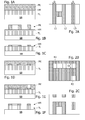
- FIGS. 1A to 1F and 2A to 2C Such a multi-transfer pattern photolithography process is illustrated by the FIGS. 1A to 1F and 2A to 2C .
- the Figures 1A to 1F represent in cross section a portion of a multilayer structure formed from a wafer made of a semiconductor material ("wafer"), at different stages of a photolithography process.
- the FIGS. 2A to 2C represent in top view a portion of the multilayer structure at some of the steps of the photolithography process.
- the multilayer structure comprises a substrate SB on which a target layer TL is formed.
- the target layer TL is covered with a hard mask layer HM, and the HM layer is covered with a layer of photoresist PR.
- line patterns formed on a first mask were transferred to the PR layer by a photolithography machine.
- the Figure 2A presents the shape of the line patterns transferred to the PR layer.
- the line patterns form parallel lines L1, L2, L3, of which two adjacent lines L1, L2 are connected by a bridge.
- the lines L1, L2, L3 formed in the treated layer have a width D that can correspond to the critical dimension of the photolithography treatment. This width is decisive on the electrical performance of components that will be formed by the line patterns in the target layer TL.
- the line patterns were transferred to the HM layer by etching treatment and the PR layer was removed.
- the HM layer is again covered with a layer of photoresist PR '.
- cutting patterns formed on a second mask were transferred to the PR 'layer by the photolithography machine.
- the Figure 2B presents the shape of the cutting patterns transferred to the PR 'layer.
- the cutting patterns form rectangular trenches R1, R2 provided for cutting lines L1, L2, L3 which have been formed in the HM layer.
- the trenches R1, R2 have a width D1 which may be greater than the critical dimension CD.
- the cutting patterns have dimensions that are not critical to the electrical performance of the components formed by the line patterns. It is simply important that the cutting patterns intersect the lines at desired locations to form separate electronic components.
- the HM layer was etched to the shape of the patterns transferred in the PR 'layer, the PR' layer was removed, and the TL target layer was etched to the shape of the patterns transferred in the HM layer.
- the Figure 2C presents the shape of the patterns thus formed in the layers HM and TL. These patterns correspond to lines L1, L2, L3 to which rectangular areas R1, R2 have been removed. The hard mask layer HM can then be completely removed.
- Embodiments are directed to a method of etching a target layer, comprising steps of: depositing a hard mask layer on a target layer and on the hard mask layer, a first layer of a photosensitive material, exposing the first layer light-sensitive layer with a particle beam through a first mask for transferring first patterns, forming the first patterns in the photosensitive layer, transferring the first patterns in the hard mask layer by etching this layer through the first layer photosensitive, depositing on the hard mask layer a second layer of photosensitive material, exposing the second photosensitive layer to a particle beam through a second mask to transfer second patterns, forming the second patterns in the second photosensitive layer , transferring the second patterns into the hard mask layer by etching this layer through the second e photosensitive layer, and transfer the first and second patterns in the target layer by etching this layer through the hard mask layer, the second patterns forming lines in the hard mask layer, and the first patterns forming trenches cutting the lines in the hard mask layer.
- the method comprises the steps of: depositing on the etched hard mask layer a third layer made of a photosensitive material, expose the third light-sensitive layer to a particle beam through a third mask for transferring third patterns, forming the third patterns in the third photosensitive layer, and transferring the third patterns in the hard mask layer by etching this layer through the third light-sensitive layer, the target layer being etched while receiving the first, second and third patterns formed in the hard mask layer, the third patterns forming lines cut by the first patterns.
- one or each of the photosensitive layers is deposited directly on the hard mask layer, previously etched or not, the photosensitive layer having a reflection coefficient of the particle beam of less than 1%, and an upper face. flat, and covers the hard mask layer without trapping gas bubbles.
- an additional layer is deposited directly on the hard mask layer, previously etched or not, one or each of the photosensitive layers being deposited on the additional layer, the method comprising a step of etching the additional layer. for transferring the patterns formed in the photosensitive layer to the additional layer.
- the additional layer has a particle beam reflection coefficient of less than 1%, and a planar upper face, and covers the hard mask layer without trapping gas bubbles.
- the upper surface of one or each of the photosensitive layers has a height variation of less than 20%, and preferably less than 15%.
- one or each of the photosensitive layers is deposited on a second hard mask layer, the second hard mask layer being deposited on the additional layer, the method comprising a step of etching the second mask layer. hard to transfer the patterns formed in the photosensitive layer to the hard mask layer.
- the target layer is a layer provided for forming gates of CMOS transistors.
- step S1 a hard mask layer HM and a layer of a photosensitive material PR are deposited successively on a target layer TL.
- the Figure 4A represents a multilayer structure that can be obtained at the end of step S1.
- the multilayer structure comprises the target layer TL to be processed by the photolithography method, the target layer being formed on a substrate SB.
- the layer TL is covered by the layer HM, and the layer HM is covered with the layer PR.
- step S2 the PR layer is subjected to a particle beam (photons, electrons, ...) through an MSK1 mask.
- Step S3 is a development step during which the exposed (or unexposed) portions are removed by the photolithography machine through the MSK1 mask.
- the Figure 4B represents the multilayer structure after the transfer of the patterns of the mask MSK1 to the PR layer.
- the Figure 5A represents the shape of the patterns transferred to the PR layer.
- the patterns transferred by the mask MSK1 to the PR layer are cutting patterns for forming trenches in the hard mask layer HM.
- the cutting patterns have a minimum dimension that may be larger than the critical dimension of the photolithography process.
- the patterns of the mask MSK1 transferred into the PR layer comprise two trenches R1, R2 of rectangular shape whose width D1 may be greater than the critical dimension of the photolithography machine used.
- step S4 is a metrology step for controlling the quality of the transfer of the mask MSK1 to the PR layer. If, on a batch of platelets, the patterns R1, R2 have larger or smaller dimensions than desired dimensions, the photolithography treatment performed in steps S2, S3 can be readjusted for a next batch of platelets. This readjustment as a function of measurement forms a control loop (here feedback type also called “Run to Run") which improves the overall quality of batches of platelets so produced.
- the measurements obtained in step S4 on a given batch of platelets can also be used to adjust on the same batch of platelets the etching parameters of the hard mask layer in the next step S5. This readjustment performed at a next step (commonly called "Feed Forward"), based on measurements obtained in a previous step, is also important for the control of manufacturing processes.
- step S5 the HM layer is etched through the PR layer to transfer the patterns formed in the PR layer to the HM layer, and the PR layer is removed.
- the figure 4C represents the multilayer structure to the outcome of step S5.
- step S6 is a metrology step for controlling the dimensions of the patterns transferred to the hard mask layer HM. If the measurements obtained in step S6 are not satisfactory, the photolithography treatment performed in steps S2, S3 can be readjusted for a next batch of platelets.
- step S7 a new layer of photoresist PR 'is deposited on the HM layer which has been etched in step S5.
- the figure 4D represents the multilayer structure at the end of step S7.
- This step is for example carried out by centrifugation, by depositing liquid resin in the center of a wafer made of a semiconductor material forming the substrate SB, and rotating the wafer.
- step S8 the resin layer PR 'is subjected to a particle beam (photons, electrons, %) through an MSK2 mask.
- Step S9 is a development step during which the exposed (or unexposed) portions are removed by the photolithography machine through the MSK2 mask.
- the figure 4E represents the multilayer structure after the transfer of the patterns of the mask MSK2 to the layer PR '.
- the patterns transferred by the mask MSK2 to the PR 'layer are line patterns having a minimum dimension which may be equal to the critical dimension of the photolithography treatment.
- the Figure 5B represents the shape of the patterns transferred to the PR 'layer. On the Figure 5B , the transferred patterns have lines L1, L2, L3, among which the adjacent lines L1, L2 are connected by a bridge.
- the lines L1, L2, L3 formed in the PR 'layer have a width D2 which may be equal to the critical dimension of the photolithography treatment. This width is decisive on the electrical performance of components that will be formed by the line patterns in the target layer TL. On the contrary, the cutting patterns R1, R2 have dimensions that are not critical to the electrical performance of the components formed by the line patterns. It is simply important that the cutting patterns intersect the lines at desired locations to form separate electronic components.
- step S10 is a metrology step for controlling the dimensions of the patterns transferred to the PR 'layer. If at step S10, the dimensions of the patterns transferred in the PR layer were greater than or equal to less than desired dimensions, the photolithography treatment performed in steps S8, S9 can be readjusted for a next batch of platelets.
- step S11 the HM layer is etched to the shape of the patterns transferred in the PR 'layer, and the PR' layer is removed. If in step S10, the dimensions of the transferred patterns in the PR 'layer were larger than desired dimensions, the etching process of the HM layer can be extended. The target layer TL is then etched to the shape of the patterns R1, R2, L1, L2, L3 transferred to the HM layer.
- the figure 4F represents the multilayer structure at the end of the etching process in step S11.
- the Figure 5C presents the shape of the patterns formed in the HM and TL layers. These patterns correspond to lines L1, L2, L3 to which rectangular areas R1, R2 have been removed. The hard mask layer HM can then be completely removed.
- the following step S12 is a metrology step to determine in particular whether the dimensions of the transferred patterns in the target layer TL correspond to those desired. If the measurements obtained in step S12 are not satisfactory, the photolithography treatments carried out in steps S2, S3 and S8, S9 can be readjusted for a following batch of platelets.
- the etching treatments of the hard mask layer have a reducing effect on the critical dimension of the patterns formed in this layer and therefore in the target layer.
- the L1, L2, L3 patterns transferred in the PR 'layer have a critical dimension of 52 nm, and when they are transferred into the target layer TL, they can reach a dimension of 34 nm.
- the metrology steps are for example carried out using a scanning electron microscope SEM (Scanning Electron Microscope), or by scalerometry.
- SEM scanning Electron Microscope
- the patterns thus formed in the target layer TL make it possible, for example, to produce gates of CMOS transistors, the layer TL then being of monocrystalline polysilicon.
- the width D2 of the lines L1, L2, L3 corresponds to the length of the gates of the transistors thus formed.
- L1, L2, L3 patterns in the hard mask layer HM is not impaired by the presence of the trenches R1, R2 formed beforehand in the HM layer. Indeed, for a photosensitive layer to be correctly exposed, it is necessary that the surface to be exposed is very flat. The deposition of a photosensitive layer on the slightest relief is therefore to be avoided in particular when the structures to be formed are very critical as regards their dimensions. In the present case, the deposition of the photosensitive layer PR 'on the trenches R1, R2 formed in the HM layer was therefore to be avoided.
- the deposition on the hard mask layer HM of a layer having planarizing and anti-reflective properties may be sufficient to overcome the presence of relief (trenches R1, R2) in the HM layer.
- the resin used to form the PR 'layer may be chosen to cover the HM layer by penetrating the trenches R1, R2 formed in step S5 without trapping gas bubbles, and have a sufficiently flat and anti -reflective, after its deposition on the HM layer to not affect the subsequent photolithography and etching of the hard mask layer HM.
- the layer deposited on the hard mask layer HM it is desirable for the layer deposited on the hard mask layer HM to have sufficient planarizing properties so that its upper surface has, especially on either side of the edge of a trench pattern R1, R2, a variation its height less than 20%, and preferably less than 15%, this variation being expressed as a percentage of the depth of field of the photolithography treatment employed.
- a photolithography treatment having a depth of field of 120 nm and a hard mask of 30 nm thickness
- the local variations in height induced by the presence of the trenches would represent 25% of the depth of field.
- the upper surface of the resin PR ' would also have local variations representing 25% of the depth of field, which is unacceptable in practice for a critical photolithography step.
- a layer of resin making it possible to reduce to less than 20 nm at its upper surface, the variations of height of 30 nm induced at its bottom surface through trenches, reduces local variations in height of the top surface of the resin to less than 17% of the depth of field, which is acceptable.
- the method which has just been described has the advantage of successively carrying out critical photolithography and etching processes (steps S7, S8, S9 and S11), that is to say determinants on the electrical performance of the electronic components produced. .
- the photolithography and trench etching process was carried out between the photolithography process and the final etching of the electrically critical structures.
- This advantage offers the possibility of carrying out critical photolithography and etching treatments without having to change the engraving machine.
- This also makes it possible to optimally implement "Feed Forward" type control loops.
- This method also has the advantage of having to perform only two critical dimensional checks instead of three as in the method of the prior art. Indeed, the dimensional control performed in step S4 does not concern critical reasons with respect to the formation of electronic components.
- the photosensitive resins employed have planarizing and anti-reflective properties.
- the planarizing and anti-reflective properties of the photosensitive resins are generally insufficient to reach critical dimensions of less than 100 nm.
- the anti-reflective property is characterized by a reflection coefficient of the particle beam emitted by the photolithography machine less than 1%, or 0.5%. This property can be obtained using an anti-reflective coating BARC ("Bottom Anti Reflective Coating") formed under the layer of resin PR 'and possibly under the PR layer.
- BARC Bottom Anti Reflective Coating
- the BARC coating can be produced by coating an antireflective resin, or by deposition (CVD - Chemical Vapor Deposition, PECVD - Plasma-Enhanced Chemical Vapor Deposition, ...) of an organic layer (for example amorphous carbon) and / or a dielectric layer (for example silicon oxide SiO 2 , silicon nitride Si 3 N 4 , ).
- CVD - Chemical Vapor Deposition PECVD - Plasma-Enhanced Chemical Vapor Deposition, ...) of an organic layer (for example amorphous carbon) and / or a dielectric layer (for example silicon oxide SiO 2 , silicon nitride Si 3 N 4 , .
- FIG. 6 represents a multilayer structure that can be formed in steps S1 and S7.
- the hard mask layer HM deposited on the target layer TL is covered with an AL layer made of an anti-reflective and planarizing material, for example based on carbon.
- the layer AL is covered with a hard mask layer HM1, on which is deposited the photoresist layer PR, PR '.
- the HM and HM1 layers may be formed of silicon oxide, silicon nitride, or TiN titanium nitride.
- the AL layer is made of a material capable of covering the HM layer by penetrating into the trenches formed in step S5 without trapping gas bubbles, and having a planar upper face after its deposition on the HM layer.
- the AL layer also has antireflective properties, that is to say a reflection coefficient of the particle beam emitted by the photolithography machine less than 1%.
- the AL layer can comprise an organic film (for example carbon) deposited by centrifugation or by CVD or PECVD.
- the layers AL, HM1 and PR are reformed with each transfer of mask patterns to the HM layer.
- the different layers deposited on the target layer TL may be formed by PVD (Physical Vapor Deposition) or CVD, or by centrifugation.
- the development processes of the PR, PR 'photosensitive layers after exposure, and the etching treatments of the hard mask layers HM, HM1, of the AL layer and of the target layer TL, are adapted to the dimensions to be obtained and to the materials to be etched. , and can implement known techniques.
- steps S7 to S10 can be repeated with masks forming complementary patterns such that the combination of masks can form high density structures.
- These high density structures are generally cut after formation in the hard mask layer and before their final transfer into the layer to be etched.
- the steps of forming areas to be removed (trenches) in the hard mask layer are performed prior to the multiple steps of forming the high density structures (lines).
- the Figures 7A to 7E illustrate different steps of a photolithography treatment for successively transferring the patterns of three masks. As previously, steps S1 to S6, corresponding to Figures 4A to 4C , are performed to transfer the patterns R1, R2 represented on the Figure 5A to the hard mask layer HM.
- a new layer of a photosensitive material PR ' is deposited on the HM layer.
- Reasons such as those depicted on the Figures 7A, 8A are transferred to the PR 'layer.
- the patterns comprise three parallel lines L4, L5, L6 whose width may be equal to the critical dimension of the photolithography treatment.
- lines L5, L6, L7 form trenches in the PR 'layer.
- the patterns formed in the PR 'layer are then transferred into the HM layer, as illustrated by the Figure 7B .
- the HM layer is excavated both by the trenches corresponding to the lines L4, L5, L6 and the trenches corresponding to the rectangular zones R1, R2 ( Figure 5A ).
- the new transferred patterns comprise parallel lines L7, L8, L9 which are transferred into the PR layer "forming trenches between the lines L4, L5, L6, the PR layer" makes it possible to transfer the patterns L7, L8, L9 to the HM layer as shown on the Figures 7D and 8D .
- the HM layer collects trenches R1, R2, and lines L4 to L9.
- the target layer TL is then etched to the patterns formed in the HM layer.
- the lines between the trenches formed by lines L4 to L9 form, for example, gates of CMOS transistors.
- the present invention is capable of various alternative embodiments and various applications.
- the invention is not limited to the etching of a polysilicon layer to form transistors gates, but can be applied to the etching of hard mask layers for doping zones of the substrate or of a layer of semiconductor material, or etchings of various layers formed on a wafer of a semiconductor material.
- the various layers presented on the figure 6 can be deposited only to perform the second etching of the hard mask layer HM and any subsequent etchings.
- the present invention is also not limited to rectangular-shaped patterns for line and cut patterns. Other more complex polygonal pattern shapes can of course be transferred to the hard mask layer and the target layer.
Landscapes
- Engineering & Computer Science (AREA)
- Manufacturing & Machinery (AREA)
- Computer Hardware Design (AREA)
- Microelectronics & Electronic Packaging (AREA)
- Power Engineering (AREA)
- Condensed Matter Physics & Semiconductors (AREA)
- Physics & Mathematics (AREA)
- General Physics & Mathematics (AREA)
- Chemical & Material Sciences (AREA)
- Inorganic Chemistry (AREA)
- Drying Of Semiconductors (AREA)
- Exposure And Positioning Against Photoresist Photosensitive Materials (AREA)
- Photosensitive Polymer And Photoresist Processing (AREA)
Abstract
Description
La présente invention concerne un procédé de fabrication de composants électroniques sur un substrat semi-conducteur. Elle concerne en particulier les procédés de photolithographie mettant en oeuvre des étapes successives de gravure de motifs dans une couche dite de "masque dur" ("hard mask") déposée sur une couche cible.The present invention relates to a method for manufacturing electronic components on a semiconductor substrate. In particular, it relates to photolithography processes employing successive etching steps of patterns in a layer called "hard mask" ("hard mask") deposited on a target layer.
Les procédés de photolithographie consistent à graver des motifs à l'aide d'une couche en un matériau photosensible, tel qu'une résine photosensible ("photoresist") déposée sur une couche cible à traiter formée sur un substrat. Une couche appelée "masque dur" ("hard mask") peut être déposée sur la couche cible avant de déposer la couche de résine photosensible. Le motif à transférer à la couche cible est alors transféré à la couche de résine par photolithographie, puis par gravure à la couche de masque dur et à la couche cible. Un transfert de motifs à la couche de résine photosensible consiste généralement à exposer la couche dans une machine de photolithographie à un faisceau de particules au travers d'un masque présentant les motifs à transférer, puis à retirer les parties exposées (dans le cas d'une résine positive) ou non exposées (dans le cas d'une résine négative) à l'aide d'un solvant de développement. La taille minimum des motifs susceptibles d'être transférés à une couche photosensible est appelée "dimension critique" (CD) et correspond par exemple à la largeur d'une ligne de motif. La dimension critique dépend de caractéristiques de la machine d'exposition de photolithographie et notamment du dispositif de projection optique, et des caractéristiques de l'exposition, du développement et du matériau photosensible utilisé.Photolithography processes involve etching patterns using a layer of a photosensitive material, such as a photoresist, deposited on a target layer to be treated formed on a substrate. A layer called "hard mask" may be deposited on the target layer before depositing the photoresist layer. The pattern to be transferred to the target layer is then transferred to the resin layer by photolithography, followed by etching to the hard mask layer and the target layer. A transfer of patterns to the photoresist layer generally involves exposing the layer in a photolithography machine to a particle beam through a mask having the patterns to be transferred, and then removing the exposed portions (in the case of a positive resin) or unexposed (in the case of a negative resin) using a developing solvent. The minimum size of the patterns that can be transferred to a photosensitive layer is called the "critical dimension" (CD) and corresponds, for example, to the width of a pattern line. The critical dimension depends on characteristics of the photolithography exposure machine and in particular the optical projection device, and the characteristics of the exposure, the development and the photosensitive material used.
Pour réduire davantage la dimension critique de motifs susceptibles d'être gravés dans une couche cible sans changer de machine de photolithographie, on a développé plusieurs procédés de transferts multiples de motifs ("multiple patterning"). Certains de ces procédés consistent à transférer successivement plusieurs motifs à une couche de masque dur formée sur la couche cible, en redéposant une nouvelle couche de résine sur la couche de masque dur entre chaque transfert. Selon un procédé de transfert multiple décrit dans le brevet
Un tel procédé de photolithographie à transferts multiples de motifs est illustré par les
Sur la
Sur la
En pratique, tous les traitements entre la gravure des lignes et la gravure finale de la couche de masque dur ont un effet réducteur de la dimension critique des motifs formés dans cette couche et donc dans la couche cible. Chaque traitement de gravure est donc suivi d'une étape de métrologie durant laquelle sont mesurés différents paramètres incluant la dimension critique. Le traitement de photolithographie formant les motifs de ligne dans la couche PR peut être adapté si la dimension critique mesurée dévie de celle à atteindre. De même, les mesures obtenues à la suite la première gravure de la couche de masque dur HM (
Toutes les étapes de traitement affectent la dimension critique sauf l'étape de photolithographie de la couche PR'. Cette étape pourrait donc être effectuée avec une machine de photolithographie moins précise et donc moins coûteuse que celle devant être utilisée pour les autres étapes de photolithographie. Cependant, un changement de machine de photolithographie durant un procédé de "multiple patterning" à la dimension critique soulève plusieurs problèmes délicats et notamment des problèmes d'alignement des deux motifs de masque à transférer sur la plaquette de semi-conducteur. Lors du traitement des structures à dimension critique, les mesures obtenues lors du premier traitement de gravure du masque dur doivent pouvoir être utilisées pour ajuster le second traitement de gravure du masque dur. Si un changement de machine est intervenu entre ces deux traitements de gravure du masque dur, ces mesures doivent être sauvegardées et introduites dans la machine assurant le second traitement de gravure du masque dur.All processing steps affect the critical dimension except the photolithography step of the PR 'layer. This step could therefore be performed with a photolithography machine less accurate and therefore less expensive than that to be used for the other photolithography steps. However, a change of photolithography machine during a process of "multiple patterning" to the critical dimension raises several delicate problems including alignment problems of the two mask patterns to be transferred to the wafer. semiconductor. When processing critical dimension structures, the measurements obtained during the first hard mask etching process must be able to be used to adjust the second etching process of the hard mask. If a machine change has occurred between these two hard mask etching processes, these measurements must be saved and introduced into the machine providing the second hard mask etching process.
Il est donc souhaitable de simplifier un tel procédé de "multiple patterning". Il est également souhaitable de réduire le temps d'utilisation d'une machine de photolithographie coûteuse, notamment en permettant l'utilisation d'une machine de photolithographie moins coûteuse pour les traitements n'intervenant pas à la dimension critique.It is therefore desirable to simplify such a method of "multiple patterning". It is also desirable to reduce the time of use of an expensive photolithography machine, in particular by allowing the use of a less expensive photolithography machine for non-critical size processing.
Des modes de réalisation concernent un procédé de gravure d'une couche cible, comprenant des étapes consistant à : déposer une couche de masque dur sur une couche cible et sur la couche de masque dur, une première couche en un matériau photosensible, exposer la première couche photosensible à un faisceau de particules au travers d'un premier masque pour transférer des premiers motifs, former les premiers motifs dans la couche photosensible, transférer les premiers motifs dans la couche de masque dur par gravure de cette couche au travers de la première couche photosensible, déposer sur la couche de masque dur gravée une seconde couche en un matériau photosensible, exposer la seconde couche photosensible à un faisceau de particules au travers d'un second masque pour transférer des seconds motifs, former les seconds motifs dans la seconde couche photosensible, transférer les seconds motifs dans la couche de masque dur par gravure de cette couche au travers de la seconde couche photosensible, et transférer les premiers et seconds motifs dans la couche cible par gravure de cette couche au travers de la couche de masque dur, les seconds motifs formant des lignes dans la couche de masque dur, et les premiers motifs formant des tranchées coupant les lignes dans la couche de masque dur.Embodiments are directed to a method of etching a target layer, comprising steps of: depositing a hard mask layer on a target layer and on the hard mask layer, a first layer of a photosensitive material, exposing the first layer light-sensitive layer with a particle beam through a first mask for transferring first patterns, forming the first patterns in the photosensitive layer, transferring the first patterns in the hard mask layer by etching this layer through the first layer photosensitive, depositing on the hard mask layer a second layer of photosensitive material, exposing the second photosensitive layer to a particle beam through a second mask to transfer second patterns, forming the second patterns in the second photosensitive layer , transferring the second patterns into the hard mask layer by etching this layer through the second e photosensitive layer, and transfer the first and second patterns in the target layer by etching this layer through the hard mask layer, the second patterns forming lines in the hard mask layer, and the first patterns forming trenches cutting the lines in the hard mask layer.
Selon un mode de réalisation, entre les étapes de seconde gravure de la couche de masque dur et de gravure de la couche cible, le procédé comprend des étapes consistant à : déposer sur la couche de masque dur gravée une troisième couche en un matériau photosensible, exposer la troisième couche photosensible à un faisceau de particules au travers d'un troisième masque pour transférer des troisièmes motifs, former les troisièmes motifs dans la troisième couche photosensible, et transférer les troisièmes motifs dans la couche de masque dur par gravure de cette couche au travers de la troisième couche photosensible, la couche cible étant gravée en recevant les premiers, seconds et troisièmes motifs formés dans la couche de masque dur, les troisièmes motifs formant des lignes coupées par les premiers motifs.According to one embodiment, between the steps of second etching of the hard mask layer and the etching of the target layer, the method comprises the steps of: depositing on the etched hard mask layer a third layer made of a photosensitive material, expose the third light-sensitive layer to a particle beam through a third mask for transferring third patterns, forming the third patterns in the third photosensitive layer, and transferring the third patterns in the hard mask layer by etching this layer through the third light-sensitive layer, the target layer being etched while receiving the first, second and third patterns formed in the hard mask layer, the third patterns forming lines cut by the first patterns.
Selon un mode de réalisation, l'une ou chacune des couches photosensibles est déposée directement sur la couche de masque dur, préalablement gravée ou non, la couche photosensible présentant un coefficient de réflexion du faisceau de particules inférieur à 1%, et une face supérieure plane, et couvre la couche de masque dur sans emprisonner de bulles de gaz.According to one embodiment, one or each of the photosensitive layers is deposited directly on the hard mask layer, previously etched or not, the photosensitive layer having a reflection coefficient of the particle beam of less than 1%, and an upper face. flat, and covers the hard mask layer without trapping gas bubbles.
Selon un mode de réalisation, une couche supplémentaire est déposée directement sur la couche de masque dur, préalablement gravée ou non, l'une ou chacune des couches photosensibles étant déposée sur la couche supplémentaire, le procédé comprenant une étape de gravure de la couche supplémentaire pour transférer les motifs formés dans la couche photosensible à la couche supplémentaire.According to one embodiment, an additional layer is deposited directly on the hard mask layer, previously etched or not, one or each of the photosensitive layers being deposited on the additional layer, the method comprising a step of etching the additional layer. for transferring the patterns formed in the photosensitive layer to the additional layer.
Selon un mode de réalisation, la couche supplémentaire présente un coefficient de réflexion du faisceau de particules inférieur à 1%, et une face supérieure plane, et couvre la couche de masque dur sans emprisonner de bulles de gaz.According to one embodiment, the additional layer has a particle beam reflection coefficient of less than 1%, and a planar upper face, and covers the hard mask layer without trapping gas bubbles.
Selon un mode de réalisation, la surface supérieure de l'une ou de chacune des couches photosensibles présente une variation de hauteur inférieure à 20%, et de préférence, inférieure à 15%.According to one embodiment, the upper surface of one or each of the photosensitive layers has a height variation of less than 20%, and preferably less than 15%.
Selon un mode de réalisation, l'une ou chacune des couches photosensibles est déposée sur une seconde couche de masque dur, la seconde couche de masque dur étant déposée sur la couche supplémentaire, le procédé comprenant une étape de gravure de la seconde couche de masque dur pour transférer les motifs formés dans la couche photosensible à la couche de masque dur.According to one embodiment, one or each of the photosensitive layers is deposited on a second hard mask layer, the second hard mask layer being deposited on the additional layer, the method comprising a step of etching the second mask layer. hard to transfer the patterns formed in the photosensitive layer to the hard mask layer.
Selon un mode de réalisation, la couche cible est une couche prévue pour former des grilles de transistors CMOS.According to one embodiment, the target layer is a layer provided for forming gates of CMOS transistors.
Des exemples de réalisation de l'invention seront décrits dans ce qui suit, à titre non limitatif en relation avec les figures jointes parmi lesquelles :
- les
figures 1A à 1F décrites précédemment représentent en coupe transversale une partir d'une structure multicouche formée à partir d'une plaquette en un matériau semi-conducteur, à différentes étapes d'un procédé de photolithographie, - les
figures 2A à 2C décrites précédemment représentent en vue de dessus la partie de structure multicouche à certaines des étapes du procédé de photolithographie, - la
figure 3 représente une séquence d'étapes d'un procédé de photolithographie, selon un mode de réalisation, - les
figures 4A à 4F représentent en coupe transversale une partie de structure multicouche formée à partir d'une plaquette en un matériau semi-conducteur, à différentes étapes du procédé de photolithographie, - les
figures 5A à 5C représentent en vue de dessus la partie de structure multicouche à certaines des étapes du procédé de photolithographie, - la
figure 6 représente une partie de structure multicouche formée dans un procédé de photolithographie, selon un autre mode de réalisation, - les
figures 7A à 7E représentent en coupe transversale une partie de structure multicouche, à différentes étapes d'un procédé de photolithographie, selon un autre mode de réalisation, - les
figures 8A à 8D représentent en vue de dessus la structure multicouche à certaines des étapes du procédé de photolithographie. - La
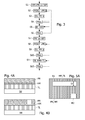
figure 3 représente une séquence d'étapes d'un traitement de photolithographie d'une couche cible dans une structure multicouche formée sur un substrat par exemple en un matériau semi-conducteur. La séquence d'étapes comprend des étapes S1 à S12. La couche cible est la couche dans laquelle des motifs doivent être transférés par exemple pour réaliser des composants électroniques de circuit intégré.
- the
Figures 1A to 1F previously described represent in cross section a part of a multilayer structure formed from a wafer made of a semiconductor material, at different stages of a photolithography process, - the
FIGS. 2A to 2C previously described represent in view from above the multilayer structure portion at some of the steps of the photolithography process, - the
figure 3 represents a sequence of steps of a photolithography process, according to an embodiment, - the
Figures 4A to 4F represent in cross section a multilayer structure part formed from a wafer made of a semiconductor material, at different stages of the photolithography process, - the
FIGS. 5A to 5C represent in plan view the multilayer structure portion at some of the steps of the photolithography process, - the
figure 6 represents a multilayer structure portion formed in a photolithography process, according to another embodiment, - the
Figures 7A to 7E represent in cross section a part of multilayer structure, at different stages of a photolithography process, according to another embodiment, - the
Figures 8A to 8D represent in top view the multilayer structure at some of the steps of the photolithography process. - The
figure 3 represents a sequence of steps of a photolithography process of a target layer in a multilayer structure formed on a substrate for example of a semiconductor material. The sequence of steps comprises steps S1 to S12. The target layer is the layer in which patterns must be transferred for example to produce electronic integrated circuit components.
A l'étape S1, une couche de masque dur HM et une couche en un matériau photosensible PR sont déposées successivement sur une couche cible TL. La
A l'étape S2, la couche PR est soumise à un faisceau de particules (photons, électrons, ...) au travers d'un masque MSK1. L'étape S3 est une étape de développement durant laquelle sont retirées les parties exposées (ou non exposées) par la machine de photolithographie au travers du masque MSK1. La
L'étape S4 qui suit est une étape de métrologie permettant de contrôler la qualité du transfert du masque MSK1 à la couche PR. Si, sur un lot de plaquettes, les motifs R1, R2 présentent des dimensions supérieures ou inférieures à des dimensions souhaitées, le traitement de photolithographie réalisé aux étapes S2, S3 peut être réajusté pour un lot de plaquettes suivant. Ce réajustement en fonction de mesure forme une boucle de régulation (ici de type rétroaction également appelé "Run to Run") qui permet d'améliorer la qualité globale des lots de plaquettes ainsi produits. Les mesures obtenues à l'étape S4 sur un lot de plaquettes donné, peuvent également être utilisées pour ajuster sur ce même lot de plaquettes, les paramètres gravure de la couche de masque dur à l'étape de S5 suivante. Ce réajustement effectué à une étape suivante (couramment appelé "Feed Forward"), basé sur des mesures obtenues à une étape précédente, est également d'importance pour la maîtrise des procédés de fabrication.The following step S4 is a metrology step for controlling the quality of the transfer of the mask MSK1 to the PR layer. If, on a batch of platelets, the patterns R1, R2 have larger or smaller dimensions than desired dimensions, the photolithography treatment performed in steps S2, S3 can be readjusted for a next batch of platelets. This readjustment as a function of measurement forms a control loop (here feedback type also called "Run to Run") which improves the overall quality of batches of platelets so produced. The measurements obtained in step S4 on a given batch of platelets can also be used to adjust on the same batch of platelets the etching parameters of the hard mask layer in the next step S5. This readjustment performed at a next step (commonly called "Feed Forward"), based on measurements obtained in a previous step, is also important for the control of manufacturing processes.
La forme et les dimensions des motifs R1, R2 ainsi transférés ne sont pas déterminantes sur la qualité du résultat final du traitement de la couche cible TL. A l'étape S5, la couche HM est gravée au travers de la couche PR, afin de transférer les motifs formés dans la couche PR à la couche HM, et la couche PR est retirée. La
A l'étape S7, une nouvelle couche de résine photosensible PR' est déposée sur la couche HM qui a été gravée à l'étape S5. La
L'étape S9 est une étape de développement durant laquelle sont retirées les parties exposées (ou non exposées) par la machine de photolithographie au travers du masque MSK2. La
L'étape S10 qui suit est une étape de métrologie visant à contrôler les dimensions des motifs transférés à la couche PR'. Si à l'étape S10, les dimensions des motifs transférés dans la couche PR' étaient supérieures ou inférieures à des dimensions souhaitées, le traitement de photolithographie réalisé aux étapes S8, S9 peut être réajusté pour un lot de plaquettes suivant. A l'étape S11, la couche HM est gravée à la forme des motifs transférés dans la couche PR', et la couche PR' est retirée. Si à l'étape S10, les dimensions des motifs transférés dans la couche PR' étaient supérieures à des dimensions souhaitées, le traitement de gravure de la couche HM peut être prolongé. La couche cible TL est ensuite gravée à la forme des motifs R1, R2, L1, L2, L3 transférés à la couche HM. La
Les traitements de gravure de la couche de masque dur ont un effet réducteur de la dimension critique des motifs formés dans cette couche et donc dans la couche cible. Ainsi, dans un exemple de réalisation, les motifs L1, L2, L3 transférés dans la couche PR' présentent une dimension critique de 52 nm, et lorsqu'ils sont transférés dans la couche cible TL, ils peuvent atteindre une dimension de 34 nm. Les étapes de métrologie sont par exemple effectuées à l'aide d'un microscope électronique à balayage SEM (Scanning Electron Microscope), ou par scattérométrie. Les motifs ainsi formés dans la couche cible TL permettent de réaliser par exemple des grilles de transistors CMOS, la couche TL étant alors en polysilicium monocristallin. La largeur D2 des lignes L1, L2, L3 correspond à la longueur des grilles des transistors ainsi formés. Ces lignes présentent donc une dimension (leur largeur) qui est déterminante sur les performances électriques de ces transistors. Au contraire, aucune des dimensions des motifs R1, R2 n'est déterminante sur les performances électriques de ces transistors. Seule la présence des tranchées R1, R2 est nécessaire pour séparer les grilles de transistors formées collectivement par les lignes L1, L2, L3.The etching treatments of the hard mask layer have a reducing effect on the critical dimension of the patterns formed in this layer and therefore in the target layer. Thus, in one exemplary embodiment, the L1, L2, L3 patterns transferred in the PR 'layer have a critical dimension of 52 nm, and when they are transferred into the target layer TL, they can reach a dimension of 34 nm. The metrology steps are for example carried out using a scanning electron microscope SEM (Scanning Electron Microscope), or by scalerometry. The patterns thus formed in the target layer TL make it possible, for example, to produce gates of CMOS transistors, the layer TL then being of monocrystalline polysilicon. The width D2 of the lines L1, L2, L3 corresponds to the length of the gates of the transistors thus formed. These lines therefore have a dimension (their width) which is decisive on the electrical performance of these transistors. On the contrary, none of the dimensions of the patterns R1, R2 is decisive on the electrical performance of these transistors. Only the presence of trenches R1, R2 is necessary for separating the gates of transistors collectively formed by the lines L1, L2, L3.
On observe que la formation de motifs L1, L2, L3 dans la couche de masque dur HM n'est pas altérée par la présence des tranchées R1, R2 formées au préalable dans la couche HM. En effet, pour qu'une couche photosensible soit correctement exposée, il est nécessaire que la surface à exposer soit très plane. Le dépôt d'une couche photosensible sur le moindre relief est donc à éviter en particulier lorsque les structures à former sont très critiques en ce qui concerne leurs dimensions. Dans le cas présent, le dépôt de la couche photosensible PR' sur les tranchées R1, R2 formées dans la couche HM était donc à éviter. Il s'avère que le dépôt sur la couche de masque dur HM d'une couche présentant des propriétés planarisante et anti-réflective peut être suffisant pour s'affranchir de la présence de relief (tranchées R1, R2) dans la couche HM. Ainsi, la résine employée pour former la couche PR' peut être choisie afin de couvrir la couche HM en pénétrant dans les tranchées R1, R2 formées à l'étape S5 sans emprisonner de bulles de gaz, et présenter une face supérieure suffisamment plane et anti-réflective, à l'issue de son dépôt sur la couche HM pour ne pas affecter les traitements suivants de photolithographie et de gravure de la couche de masque dur HM. En pratique, il est souhaitable que la couche déposée sur la couche de masque dur HM possède des propriétés planarisantes suffisantes pour que sa surface supérieure présente, notamment de part et d'autre du bord d'un motif de tranchée R1, R2, une variation de sa hauteur inférieure à 20%, et de préférence, inférieure à 15%, cette variation étant exprimée en pourcentage de la profondeur de champ du traitement de photolithographie employé. Par exemple, pour un traitement de photolithographie présentant une profondeur de champ de 120 nm et un masque dur de 30 nm d'épaisseur, les variations locales de hauteur induites par la présence des tranchées représenteraient 25% de la profondeur de champ. En l'absence de couche présentant des propriétés planarisantes suffisantes, la surface supérieure de la résine PR' présenterait elle aussi des variations locales représentant 25% de la profondeur de champ, ce qui est inacceptable en pratique pour une étape de photolithographie critique. En revanche, une couche de résine permettant de réduire à moins de 20 nm à sa surface supérieure, les variations de hauteur de 30 nm induites à sa surface inférieure par les tranchées, permet de réduire les variations locales de hauteur de la surface supérieure de la résine à moins de 17% de la profondeur de champ, ce qui est acceptable.It is observed that the formation of L1, L2, L3 patterns in the hard mask layer HM is not impaired by the presence of the trenches R1, R2 formed beforehand in the HM layer. Indeed, for a photosensitive layer to be correctly exposed, it is necessary that the surface to be exposed is very flat. The deposition of a photosensitive layer on the slightest relief is therefore to be avoided in particular when the structures to be formed are very critical as regards their dimensions. In the present case, the deposition of the photosensitive layer PR 'on the trenches R1, R2 formed in the HM layer was therefore to be avoided. It turns out that the deposition on the hard mask layer HM of a layer having planarizing and anti-reflective properties may be sufficient to overcome the presence of relief (trenches R1, R2) in the HM layer. Thus, the resin used to form the PR 'layer may be chosen to cover the HM layer by penetrating the trenches R1, R2 formed in step S5 without trapping gas bubbles, and have a sufficiently flat and anti -reflective, after its deposition on the HM layer to not affect the subsequent photolithography and etching of the hard mask layer HM. In practice, it is desirable for the layer deposited on the hard mask layer HM to have sufficient planarizing properties so that its upper surface has, especially on either side of the edge of a trench pattern R1, R2, a variation its height less than 20%, and preferably less than 15%, this variation being expressed as a percentage of the depth of field of the photolithography treatment employed. For example, for a photolithography treatment having a depth of field of 120 nm and a hard mask of 30 nm thickness, the local variations in height induced by the presence of the trenches would represent 25% of the depth of field. In the absence of a layer having sufficient planarizing properties, the upper surface of the resin PR 'would also have local variations representing 25% of the depth of field, which is unacceptable in practice for a critical photolithography step. On the other hand, a layer of resin making it possible to reduce to less than 20 nm at its upper surface, the variations of height of 30 nm induced at its bottom surface through trenches, reduces local variations in height of the top surface of the resin to less than 17% of the depth of field, which is acceptable.
Le procédé qui vient d'être décrit présente l'avantage de réaliser successivement les traitements de photolithographie et de gravure critiques (étapes S7, S8, S9 et S11), c'est-à-dire déterminants sur les performances électriques des composants électroniques réalisés. Dans l'art antérieur, le traitement de photolithographie et de gravure des tranchées était effectué entre le traitement de photolithographie et la gravure finale des structures électriquement critiques. Cet avantage offre la possibilité de réaliser les traitements de photolithographie et de gravure critiques sans avoir à changer de machine de gravure. Cela permet aussi de mettre en oeuvre de manière optimale des boucles de régulation de type "Feed Forward". Ce procédé présente également l'avantage de n'avoir à effectuer que deux contrôles dimensionnels critiques au lieu de trois comme dans le procédé de l'art antérieur. En effet, le contrôle dimensionnel effectué à l'étape S4 ne concerne pas des motifs critiques en ce qui concerne la formation des composants électroniques.The method which has just been described has the advantage of successively carrying out critical photolithography and etching processes (steps S7, S8, S9 and S11), that is to say determinants on the electrical performance of the electronic components produced. . In the prior art, the photolithography and trench etching process was carried out between the photolithography process and the final etching of the electrically critical structures. This advantage offers the possibility of carrying out critical photolithography and etching treatments without having to change the engraving machine. This also makes it possible to optimally implement "Feed Forward" type control loops. This method also has the advantage of having to perform only two critical dimensional checks instead of three as in the method of the prior art. Indeed, the dimensional control performed in step S4 does not concern critical reasons with respect to the formation of electronic components.
En pratique, pour atteindre une largeur de ligne D2 de l'ordre de 30 nm, les résines photosensibles employées présentent des propriétés planarisantes et anti-réflectives. Les propriétés planarisantes et anti-réflectives des résines photosensibles sont généralement insuffisantes pour atteindre des dimensions critiques inférieures à 100 nm. La propriété anti-réflective est caractérisée par un coefficient de réflexion du faisceau de particules émis par la machine de photolithographie inférieur à 1%, ou 0,5%. Cette propriété peut être obtenue à l'aide d'un revêtement anti-réflectif BARC ("Bottom Anti Reflective Coating") formé sous la couche de résine PR' et éventuellement sous la couche PR. Le revêtement BARC peut être réalisé par couchage d'une résine antiréflective, ou par dépôt (CVD - Chemical Vapor Deposition, PECVD - Plasma-Enhanced Chemical Vapor Deposition, ...) d'une couche organique (par exemple en carbone amorphe) et/ou d'une couche diélectrique (par exemple en oxyde de silicium SiO2, nitrure de silicium Si3N4, ...).In practice, to achieve a line width D2 of the order of 30 nm, the photosensitive resins employed have planarizing and anti-reflective properties. The planarizing and anti-reflective properties of the photosensitive resins are generally insufficient to reach critical dimensions of less than 100 nm. The anti-reflective property is characterized by a reflection coefficient of the particle beam emitted by the photolithography machine less than 1%, or 0.5%. This property can be obtained using an anti-reflective coating BARC ("Bottom Anti Reflective Coating") formed under the layer of resin PR 'and possibly under the PR layer. The BARC coating can be produced by coating an antireflective resin, or by deposition (CVD - Chemical Vapor Deposition, PECVD - Plasma-Enhanced Chemical Vapor Deposition, ...) of an organic layer (for example amorphous carbon) and / or a dielectric layer (for example silicon oxide SiO 2 , silicon nitride Si 3 N 4 , ...).
Une autre solution consiste à associer les couches PR et PR' à une couche de masque dur et une couche en un matériau planarisant et anti-réflectif, non nécessairement photosensible. La
Pour augmenter la densité des structures transférées dans la couche HM, les étapes S7 à S10 peuvent être répétées avec des masques formant des motifs complémentaires tels que la combinaison des masques permet de former des structures à haute densité. Ces structures à haute densité sont généralement coupées après leur formation dans la couche de masque dur et avant leur transfert final dans la couche à graver. Selon un mode de réalisation, les étapes de formation de zones à supprimer (tranchées) dans la couche de masque dur sont réalisées avant les étapes multiples de formation des structures à haute densité (lignes). Les
Sur la
Le procédé qui vient d'être décrit (mettant en oeuvre trois projections de masque) permet ainsi d'atteindre un espacement de lignes deux fois plus petit que celui obtenu par le procédé utilisant précédent, mettant en oeuvre deux projections de masque (
Il apparaîtra clairement à l'homme de l'art que la présente invention est susceptible de diverses variantes de réalisation et diverses applications. En particulier, l'invention n'est pas limitée à la gravure d'une couche en polysilicium pour former des grilles de transistors, mais peut s'appliquer à la gravure de couches de masques durs pour réaliser des dopages de zones du substrat ou d'une couche en un matériau semi-conducteur, ou des gravures de diverses couches formées sur une plaquette en un matériau semi-conducteur.It will be apparent to those skilled in the art that the present invention is capable of various alternative embodiments and various applications. In particular, the invention is not limited to the etching of a polysilicon layer to form transistors gates, but can be applied to the etching of hard mask layers for doping zones of the substrate or of a layer of semiconductor material, or etchings of various layers formed on a wafer of a semiconductor material.
Les diverses couches présentées sur la
La présente invention n'est pas non plus limitée à des motifs de forme rectangulaire pour les motifs de ligne et de coupe. D'autres formes de motif polygonales plus complexes peuvent bien entendu être transférées à la couche de masque dur et à la couche cible.The present invention is also not limited to rectangular-shaped patterns for line and cut patterns. Other more complex polygonal pattern shapes can of course be transferred to the hard mask layer and the target layer.
Claims (9)
et
and
Applications Claiming Priority (1)
| Application Number | Priority Date | Filing Date | Title |
|---|---|---|---|
| FR1100662A FR2972293A1 (en) | 2011-03-04 | 2011-03-04 | METHOD FOR MANUFACTURING AN INTEGRATED CIRCUIT ON THE FORMATION OF LINES AND SLICES |
Publications (2)
| Publication Number | Publication Date |
|---|---|
| EP2495754A2 true EP2495754A2 (en) | 2012-09-05 |
| EP2495754A3 EP2495754A3 (en) | 2013-12-25 |
Family
ID=45562252
Family Applications (1)
| Application Number | Title | Priority Date | Filing Date |
|---|---|---|---|
| EP12155129.5A Withdrawn EP2495754A3 (en) | 2011-03-04 | 2012-02-13 | Manufacturing method of integrated circuits based on formation of lines and trenches |
Country Status (3)
| Country | Link |
|---|---|
| US (1) | US20120225560A1 (en) |
| EP (1) | EP2495754A3 (en) |
| FR (1) | FR2972293A1 (en) |
Families Citing this family (4)
| Publication number | Priority date | Publication date | Assignee | Title |
|---|---|---|---|---|
| CN103309165A (en) * | 2012-03-09 | 2013-09-18 | 中芯国际集成电路制造(上海)有限公司 | Formation method for semiconductor structure |
| US9204538B2 (en) | 2013-08-16 | 2015-12-01 | Taiwan Semiconductor Manufacturing Company, Ltd. | Method of fine line space resolution lithography for integrated circuit features using double patterning technology |
| US9209076B2 (en) | 2013-11-22 | 2015-12-08 | Taiwan Semiconductor Manufacturing Company, Ltd. | Method of double patterning lithography process using plurality of mandrels for integrated circuit applications |
| CN111383920B (en) * | 2018-12-29 | 2024-06-18 | 中芯国际集成电路制造(上海)有限公司 | Semiconductor structure and forming method thereof |
Citations (1)
| Publication number | Priority date | Publication date | Assignee | Title |
|---|---|---|---|---|
| US6787469B2 (en) | 2001-12-28 | 2004-09-07 | Texas Instruments Incorporated | Double pattern and etch of poly with hard mask |
Family Cites Families (15)
| Publication number | Priority date | Publication date | Assignee | Title |
|---|---|---|---|---|
| US5943550A (en) * | 1996-03-29 | 1999-08-24 | Advanced Micro Devices, Inc. | Method of processing a semiconductor wafer for controlling drive current |
| US6277716B1 (en) * | 1999-10-25 | 2001-08-21 | Chartered Semiconductor Manufacturing Ltd. | Method of reduce gate oxide damage by using a multi-step etch process with a predictable premature endpoint system |
| US6686124B1 (en) * | 2000-03-14 | 2004-02-03 | International Business Machines Corporation | Multifunctional polymeric materials and use thereof |
| US6596599B1 (en) * | 2001-07-16 | 2003-07-22 | Taiwan Semiconductor Manufacturing Company | Gate stack for high performance sub-micron CMOS devices |
| AU2003240931A1 (en) * | 2002-05-29 | 2003-12-19 | Massachusetts Institute Of Technology | A method for photolithography using multiple illuminations and a single fine feature mask |
| US6645851B1 (en) * | 2002-09-17 | 2003-11-11 | Taiwan Semiconductor Manufacturing Company | Method of forming planarized coatings on contact hole patterns of various duty ratios |
| US6846360B2 (en) * | 2003-01-13 | 2005-01-25 | Aptos Corporation | Apparatus and method for bubble-free application of a resin to a substrate |
| KR100554514B1 (en) * | 2003-12-26 | 2006-03-03 | 삼성전자주식회사 | Method for forming pattern and gate electrode in semiconductor processing |
| US20070231748A1 (en) * | 2006-03-29 | 2007-10-04 | Swaminathan Sivakumar | Patterning trenches in a photoresist layer with tight end-to-end separation |
| US8158333B2 (en) * | 2006-04-11 | 2012-04-17 | Kabushiki Kaisha Toshiba | Manufacturing method of semiconductor device |
| US8017310B2 (en) * | 2007-02-02 | 2011-09-13 | Asml Netherlands B.V. | Lithographic method |
| KR100843236B1 (en) * | 2007-02-06 | 2008-07-03 | 삼성전자주식회사 | Method of forming fine patterns of semiconductor device using double patterning process |
| US8039203B2 (en) * | 2007-09-25 | 2011-10-18 | Infineon Technologies Ag | Integrated circuits and methods of design and manufacture thereof |
| US7927782B2 (en) * | 2007-12-28 | 2011-04-19 | Texas Instruments Incorporated | Simplified double mask patterning system |
| US8173544B2 (en) * | 2008-05-02 | 2012-05-08 | Texas Instruments Incorporated | Integrated circuit having interleaved gridded features, mask set and method for printing |
-
2011
- 2011-03-04 FR FR1100662A patent/FR2972293A1/en active Pending
-
2012
- 2012-02-13 EP EP12155129.5A patent/EP2495754A3/en not_active Withdrawn
- 2012-03-02 US US13/411,397 patent/US20120225560A1/en not_active Abandoned
Patent Citations (1)
| Publication number | Priority date | Publication date | Assignee | Title |
|---|---|---|---|---|
| US6787469B2 (en) | 2001-12-28 | 2004-09-07 | Texas Instruments Incorporated | Double pattern and etch of poly with hard mask |
Also Published As
| Publication number | Publication date |
|---|---|
| US20120225560A1 (en) | 2012-09-06 |
| EP2495754A3 (en) | 2013-12-25 |
| FR2972293A1 (en) | 2012-09-07 |
Similar Documents
| Publication | Publication Date | Title |
|---|---|---|
| EP0001030B1 (en) | Process for manufacturing a mask according to a given pattern on a support | |
| EP2577395B1 (en) | Lithographic pitch doubling process | |
| EP2458621B1 (en) | Improved method for making a pattern based on transfer by lateral spacers | |
| JP5644192B2 (en) | Method for forming laminated resin film and method for manufacturing semiconductor device | |
| EP2495754A2 (en) | Manufacturing method of integrated circuits based on formation of lines and trenches | |
| US20140162459A1 (en) | Methods of Forming A Pattern On A Substrate | |
| EP2577723B1 (en) | Lithography method for making networks of conductors connected by vias | |
| EP2226678B1 (en) | Process for fabricating a mould for nanoimprint lithography | |
| FR2678108A1 (en) | Method of manufacturing calibration structures, in particular for calibrating machines for measuring alignment in integrated circuits | |
| EP1290498B1 (en) | Method for creating an integrated circuit stage wherein fine and large patterns coexist | |
| EP3252830B1 (en) | Method for forming patterns by ions implantations | |
| EP0675544B1 (en) | Method of manufacturing a short channel insulated field effect transistor; and corresponding transistor | |
| EP1960835B1 (en) | Reflection lithography mask and method for making same | |
| EP3889683A1 (en) | Method for making a randomised zone of an integrated circuit | |
| EP1071122A1 (en) | Process for correcting the topography of microelectronic substrates | |
| FR2963477A1 (en) | Material pattern e.g. boron nitride material pattern, forming method for integrated circuit, involves etching covering layer via etching mask to form projecting pattern, and etching material layer via covering layer to form material pattern | |
| EP3890005B1 (en) | Method for producing on a plate a plurality of chips, each comprising an individualisation area | |
| EP2772802A1 (en) | Dual-mask photolithography method minimising the impact of substrate defects | |
| EP4398288A1 (en) | Method for transforming a support | |
| EP3985437A1 (en) | Method for manufacturing a set of electronic components on the front face of a semiconductor plate | |
| FR2646291A1 (en) | METHOD FOR PRODUCING AN ALKALINE TRANSISTOR | |
| FR2858716A1 (en) | Thin layer obtaining process for hybrid circuit, involves forming polymer and anti-reflect layers on circuit, and removing parts of both layers to locate part of remaining latter layer on side of each elementary circuit | |
| EP1800338A1 (en) | Method for producing layers located on a hybrid circuit | |
| FR2945664A1 (en) | Integrated circuit pattern realizing method, involves depositing pattern stabilizing coating at temperature less than vitreous transition temperature of resin of resin layer, before depositing another resin layer | |
| EP0807962A1 (en) | Process for making selfaligned conductive contacts for electronic devices |
Legal Events
| Date | Code | Title | Description |
|---|---|---|---|
| STAA | Information on the status of an ep patent application or granted ep patent |
Free format text: STATUS: REQUEST FOR EXAMINATION WAS MADE |
|
| PUAI | Public reference made under article 153(3) epc to a published international application that has entered the european phase |
Free format text: ORIGINAL CODE: 0009012 |
|
| 17P | Request for examination filed |
Effective date: 20120213 |
|
| AK | Designated contracting states |
Kind code of ref document: A2 Designated state(s): AL AT BE BG CH CY CZ DE DK EE ES FI FR GB GR HR HU IE IS IT LI LT LU LV MC MK MT NL NO PL PT RO RS SE SI SK SM TR |
|
| AX | Request for extension of the european patent |
Extension state: BA ME |
|
| PUAL | Search report despatched |
Free format text: ORIGINAL CODE: 0009013 |
|
| AK | Designated contracting states |
Kind code of ref document: A3 Designated state(s): AL AT BE BG CH CY CZ DE DK EE ES FI FR GB GR HR HU IE IS IT LI LT LU LV MC MK MT NL NO PL PT RO RS SE SI SK SM TR |
|
| AX | Request for extension of the european patent |
Extension state: BA ME |
|
| RIC1 | Information provided on ipc code assigned before grant |
Ipc: H01L 21/033 20060101AFI20131120BHEP Ipc: H01L 21/3213 20060101ALI20131120BHEP |
|
| STAA | Information on the status of an ep patent application or granted ep patent |
Free format text: STATUS: THE APPLICATION IS DEEMED TO BE WITHDRAWN |
|
| 18D | Application deemed to be withdrawn |
Effective date: 20140626 |