EP2493043A2 - Busbar for power conversion applications - Google Patents
Busbar for power conversion applications Download PDFInfo
- Publication number
- EP2493043A2 EP2493043A2 EP12156821A EP12156821A EP2493043A2 EP 2493043 A2 EP2493043 A2 EP 2493043A2 EP 12156821 A EP12156821 A EP 12156821A EP 12156821 A EP12156821 A EP 12156821A EP 2493043 A2 EP2493043 A2 EP 2493043A2
- Authority
- EP
- European Patent Office
- Prior art keywords
- busbar
- impedance element
- planar
- planar conductor
- conductor
- Prior art date
- Legal status (The legal status is an assumption and is not a legal conclusion. Google has not performed a legal analysis and makes no representation as to the accuracy of the status listed.)
- Granted
Links
Images





Classifications
-
- H—ELECTRICITY
- H02—GENERATION; CONVERSION OR DISTRIBUTION OF ELECTRIC POWER
- H02G—INSTALLATION OF ELECTRIC CABLES OR LINES, OR OF COMBINED OPTICAL AND ELECTRIC CABLES OR LINES
- H02G5/00—Installations of bus-bars
- H02G5/005—Laminated bus-bars
-
- H—ELECTRICITY
- H02—GENERATION; CONVERSION OR DISTRIBUTION OF ELECTRIC POWER
- H02M—APPARATUS FOR CONVERSION BETWEEN AC AND AC, BETWEEN AC AND DC, OR BETWEEN DC AND DC, AND FOR USE WITH MAINS OR SIMILAR POWER SUPPLY SYSTEMS; CONVERSION OF DC OR AC INPUT POWER INTO SURGE OUTPUT POWER; CONTROL OR REGULATION THEREOF
- H02M7/00—Conversion of AC power input into DC power output; Conversion of DC power input into AC power output
- H02M7/003—Constructional details, e.g. physical layout, assembly, wiring or busbar connections
Definitions
- the present invention relates generally to busbar designs and more particularly to an improved busbar for use in power conversion applications.
- the present invention overcomes at least some of the aforementioned drawbacks by providing an improved busbar design. More specifically, the present invention is directed to a busbar and a power conversion assembly that incorporates the busbar design resulting in reduced inductance and improved system efficiency.
- a busbar comprises: a first planar conductor having a plurality of terminal locations; a second planar conductor having a plurality of terminal locations; a first planar insulator located between the first planar conductor and the second planar conductor; a first impedance element electrically connected to the first planar conductor, wherein the first impedance element extends in a plane that is non-coplanar from the first planar conductor; a second impedance element electrically connected to the second planar conductor, wherein the second impedance element extends in a plane that is non-coplanar from the second planar conductor, further wherein the first impedance element and the second impedance element are configured so as to define a gap therebetween; and a second planar insulator located in the gap.
- a power conversion assembly comprises: a busbar comprising: a first planar conductor having a plurality of terminal locations; a second planar conductor having a plurality of terminal locations; a first planar insulator located between the first planar conductor and the second planar conductor; a first impedance element electrically connected to the first planar conductor, wherein the first impedance element extends in a plane that is non-coplanar from the first planar conductor; a second impedance element electrically connected to the second planar conductor, wherein the second impedance element extends in a plane that is non-coplanar from the second planar conductor, further wherein the first impedance element and the second impedance element are configured so as to define a gap therebetween; and a second planar insulator located in the gap; an energy source connected to the busbar; and a power switch connected to the busbar.
- the busbar conductors include an impedance element that aids in minimizing inductance so as to reduce voltage overshoots. Ultimately, the inductance across the busbar is reduced resulting in improved performance and efficiency of the power conversion assemblies that employ the improved busbar.
- the busbar 10 may comprise two substantially planar conductors 20, 30 with a first planar insulator 40 located therebetween.
- the second planar insulator 45 has been omitted for clarity purposes only (See e.g., FIGS. 2-5 ).
- the first planar conductor 20 may comprise a bottom conductor and the second planar conductor 30 may comprise a top conductor.
- the first, or bottom planar conductor 20 may include a plurality of terminal connectors 22 for connecting to one or more power switches (see e.g., FIG. 6 ).
- the second, or top planar conductor 30 may include a plurality of terminal connectors 32 for connecting to one or more power switches (see e.g., FIG. 6 ).
- the top conductor 30 and the bottom conductor 20 further include a plurality of terminal connectors 32, 22, respectively, for further connecting the busbar 10 to one or more energy sources (see e.g., FIG. 6 ).
- the busbar 10 is suitably constructed so as to be connectable to a plurality of power switches 70 ( FIG. 6 ) and a plurality of energy sources 60 ( FIG. 6 ) so as to comprise a power conversion assembly 100 (FIG.60).
- the bottom conductor 20 may further comprise a first impedance element 24 that is configured to electrically connect to the bottom conductor 20.
- the first impedance element 24 may extend in a planar fashion away from the plane of the bottom conductor 20.
- the first impedance element 24 may extend so that it is substantially perpendicular to the plane of the bottom conductor 20.
- the first impedance element 24 may be fixed to the bottom conductor 20 or in other embodiments may be removably attached to the bottom conductor 20. In an embodiment, as shown the first impedance element 24 may be L-shaped.
- the second conductor 30 may further comprise a second impedance element 34 that is configured to electrically connect to the top conductor 30.
- the second impedance element 34 may extend in a planar fashion away from the plane of the top conductor 30.
- the second impedance element 34 may extend so that it is substantially perpendicular to the plane of the top conductor 30.
- the second impedance element 34 may be fixed to the top conductor 30 or in other embodiments may be removably attached to the top conductor 30.
- the second impedance element 34 may be L-shaped.
- the first impedance element 24 and second impedance element 34 may be other shapes, for example, curved, linear, and the like.
- the first conductor 20 and the second conductor 30 may be constructed of any suitable material or combination of materials that provide suitable electrical conductivity and/or low electrical resistivity properties.
- the first conductor 20 and the second conductor 30 may comprise at least one of copper, aluminum, silver, gold, alloys thereof, metals, and combinations thereof.
- the first planar insulator 40 sandwiched between the first conductor 20 and the second conductor 30 may comprise any suitable material or combination of materials that provides suitable electrical insulation qualities between the first conductor 20 and the second conductor 30.
- the first planar insulator 40 may comprise polyimide, epoxy glass (e.g., FR4), polytetrafluoroethylene, other electrical nonconducting insulator (e.g., isolator), and the like.
- the first impedance element 24 and the second impedance element 34 may be constructed of any suitable material or combination of materials that provide suitable electrical conductivity and/or low electrical resistivity.
- busbar 10 has terminal connections 22, 32 for connecting to three power switches and three energy sources, clearly the busbar 10 may be configured to connect to other quantities and types of devices.
- FIG. 2 a close up view of one of the terminal connection areas of the busbar 10 is shown.
- the busbar 10 is configured so that the first impedance element 24 and the second impedance element 34 are substantially adjacent thereby defining a gap 50 therebetween.
- the configuration is such that the first impedance element 24 and the second impedance element 34 are substantially parallel. In this manner, impedance is further lowered across the busbar 10.
- a second planar insulator 45 is located within the gap 50.
- the second planar insulator 45 may comprise polyimide (e.g., Kapton), epoxy glass (e.g., FR4), polytetrafluoroethylene (e.g., Teflon), other electrical nonconducting insulator (e.g., Isolator), and the like.
- end and front elevation views show the relationship of the first impedance element 24 and the second impedance element 34 and the gap 50 therebetween.
- the gap 50 has a distance, d, which depending on the embodiment may be in a range from about 5 mil to about 50 mil. In other embodiments, the distance, d, of the gap 50 may be from about 1 mil to about 70 mil.
- the second planar insulator 45 is located within the gap 50 and may partially or entirely fill the gap 50.
- the height of the first impedance element 24 and the second impedance element 34 may be any suitable height out of the plane of the first planar conductor 20 and the second planar conductor 30.
- the height of the first impedance element 24 and the second impedance element 34 may be in a range from about 0.25 inch to about 1.0 inch. Clearly, other suitable sizes may be employed without departing from the invention.
- FIG. 5 depicts a schematic diagram of a portion of a busbar 10 in accordance with the present invention.
- at least one power switch 70 is connected to a busbar 10.
- At least one current source 60 is further connected to the busbar 10.
- the first impedance element 24 and the second impedance element 34 are configured so as to define a gap 50 therebetween.
- the second planar insulator 45 is located within the gap 50.
- the first impedance element 24 and the second impedance element 34 are configured so that the gap 50 is located substantially near and/or in a current path 75 between the at least one power switch 70 and the at least one current source 60.
- Both the total planar area of the first impedance element 24 and the second impedance element 34 and the gap 50 and second planar insulator 45 therebetween effect the impedance across the busbar 10.
- the elements may be configured so that the impedance across the busbar 10 is substantially reduced.
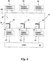
- FIG. 6 depicts a power conversion assembly, or assembly 100 that comprises a plurality of power switches 70 and a plurality of energy sources 60 both electrically connected to the busbar 10.
- the plurality of power switches 70 is further connected to a load 80.
- the load 80 may be any suitable electrical load such as, multiphase electric motors (e.g., linear or rotary), DC electric motors (e.g., linear or rotary), and/or electrical loads requiring DC power, AC power or current (e.g., MRI gradient coils which require current but not much power).
- a plurality of first impedance elements 24 and the second impedance elements 34 are configured to be substantially in the current paths between the plurality of power switches 70 and a plurality of energy sources 60. In this manner, the inductance across the busbar 10 is effectively reduced and the overall efficiency and performance of the assembly 100 is concomitantly improved.
- the quantity of power switches 70 and energy sources 60 connected to the busbar may be from one (1) to any plurality (e.g., n, wherein n approaches a near infinite quantity).
- Any suitable type of power switch 70 may be used including any mechanical element and any solid state element.
- Suitable power switches 70 include, for example, a single switch, a six-pack, a multi-switch device, a power module, a half bridge, and the like.
- any suitable energy source 60 may be used including, for example, a capacitor, an electrochemical battery, and the like.
- the size of the busbar may be established by the width of the power modules (e.g., three) on a heat sink and the distance between the positive and negative terminals of the modules and the electrical connections on the capacitors.
- the width of the power modules e.g., three
- the positive and negative voltage plates may be designed to incorporate creep distance in the vicinity of the module terminals and the connection points on the capacitors. Analysis was performed using Ansoft Q3D Extractor to calculate parasitic inductance. To perform the calculation on the busbar, the power modules and capacitors were not included in the analysis. The source and sink locations are identified and the capacitor terminals were shorted.
- FIG. 7 shows the results of the analysis of Phase A source and sink terminals showing the baseline current density in the copper positive and negative voltage plates.
- the baseline configuration excludes the first and second impedance elements in the bottom and top conductors, respectively.
- Analyses of the Phase B and Phase C configurations were also performed.
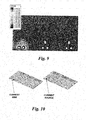
- FIG. 10 depicts a front perspective view of a finite element model from Q3D Extractor with the source and sink terminals labeled.
- the first modification (i.e., Mod 1) was to form a parallel conduction path extending vertically (substantially perpendicular to the plane of the busbar) at the module terminal location.
- FIG. 8 shows the results of the analysis showing the current density in the copper positive and negative voltage plates.
- FIGS. 11A and 11B show front perspective view, and close up view, respectively, of a finite element model from Q3D Extractor for a busbar having a first modification (Mod 1)
- the second modification (i.e., Mod 2) was to form parallel conduction paths at right angles (e.g., L-shaped) extending vertically (substantially perpendicular to the plane of the busbar) at the module terminal location.
- FIG. 9 shows the results of the analysis showing the current density in the copper positive and negative voltage plates.
- FIGS. 12A and 12B show front perspective view, and close up view, respectively, of a finite element model from Q3D Extractor for a busbar having a second modification (Mod 2) Table 1 summarized the calculate inductances and resistances for all analysis performed.
- Phase A (nH / ohms) Phase B (nH / ohms) Phase C (nH / ohms) Baseline 10.95 / 0.0052 10.47 / 0.0052 10.75 / 0.0058 Mod 1 7.75 / 0.0060 Mod 2 6.72 / 0.0081
- An embodiment of the assembly that has been tested included a power amplifier that incorporates a laminated busbar to interconnect the positive and negative terminal of each of three (3) 1200V, 450A custom power modules to DC link capacitors (e.g., three Electronic Concepts UL31 polypropylene capacitors). Three geometric configurations were analyzed. The loop inductance from the positive voltage terminal, to the capacitor, and returning to the negative voltage were 10.95 nH, 7.75 nH, and 6.72 nH for the three configurations, respectively.
- the power amplifier design, or assembly incorporates three 450A, 1200V half bridge modules, a heat sink, busbar, DC link capacitors, gate drive cards, and a controller card.
- the module includes an aluminum-silicon (AlSi) metal matrix composite (MMC) baseplate with 1mm by 3mm deep channels for integrated liquid cooling.
- the power modules are mounted to an aluminum A16061-T6 heat sink that incorporates manifolding and hydraulic interconnect to the three half bridge modules.
- the busbar is mounted to the modules and the DC link capacitors.
- the gate drive cards are mounted directly on top of each 1200V, 450A module with the busbar located between the power modules and gate drive cards.
- the controller card is mounted on top of the gate drive cards.
- a busbar comprises: a first planar conductor having a plurality of terminal locations; a second planar conductor having a plurality of terminal locations; a first planar insulator located between the first planar conductor and the second planar conductor; a first impedance element electrically connected to the first planar conductor, wherein the first impedance element extends in a plane that is non-coplanar from the first planar conductor; a second impedance element electrically connected to the second planar conductor, wherein the second impedance element extends in a plane that is non-coplanar from the second planar conductor, further wherein the first impedance element and the second impedance element are configured so as to define a gap therebetween; and a second planar insulator located in the gap.
- a power conversion assembly comprises: a busbar comprising: a first planar conductor having a plurality of terminal locations; a second planar conductor having a plurality of terminal locations; a first planar insulator located between the first planar conductor and the second planar conductor; a first impedance element electrically connected to the first planar conductor, wherein the first impedance element extends in a plane that is non-coplanar from the first planar conductor; a second impedance element electrically connected to the second planar conductor, wherein the second impedance element extends in a plane that is non-coplanar from the second planar conductor, further wherein the first impedance element and the second impedance element are configured so as to define a gap therebetween; and a second planar insulator located in the gap; an energy source connected to the busbar; and a power switch connected to the busbar.
Landscapes
- Inverter Devices (AREA)
- Structure Of Printed Boards (AREA)
Abstract
Description
- The present invention relates generally to busbar designs and more particularly to an improved busbar for use in power conversion applications.
- Current power conversion applications have increasingly faster power modules (e.g., semiconductors). Concomitant with this increased power and speed of the power conversion assemblies is the goal to minimize inductance across any interconnections in the system so as to reduce voltage overshoots. By decreasing the amount of ringup, or power spikes, less power is required to run the system, ultimately resulting in a more efficient system.
- Accordingly, there is an ongoing need in increasing overall system efficiency for power conversion assemblies including the busbar design therein.
- The present invention overcomes at least some of the aforementioned drawbacks by providing an improved busbar design. More specifically, the present invention is directed to a busbar and a power conversion assembly that incorporates the busbar design resulting in reduced inductance and improved system efficiency.
- Therefore, in accordance with one aspect of the invention, a busbar comprises: a first planar conductor having a plurality of terminal locations; a second planar conductor having a plurality of terminal locations; a first planar insulator located between the first planar conductor and the second planar conductor; a first impedance element electrically connected to the first planar conductor, wherein the first impedance element extends in a plane that is non-coplanar from the first planar conductor; a second impedance element electrically connected to the second planar conductor, wherein the second impedance element extends in a plane that is non-coplanar from the second planar conductor, further wherein the first impedance element and the second impedance element are configured so as to define a gap therebetween; and a second planar insulator located in the gap.
- In accordance with another aspect of the invention, a power conversion assembly comprises: a busbar comprising: a first planar conductor having a plurality of terminal locations; a second planar conductor having a plurality of terminal locations; a first planar insulator located between the first planar conductor and the second planar conductor; a first impedance element electrically connected to the first planar conductor, wherein the first impedance element extends in a plane that is non-coplanar from the first planar conductor; a second impedance element electrically connected to the second planar conductor, wherein the second impedance element extends in a plane that is non-coplanar from the second planar conductor, further wherein the first impedance element and the second impedance element are configured so as to define a gap therebetween; and a second planar insulator located in the gap; an energy source connected to the busbar; and a power switch connected to the busbar.
- Various other features and advantages of the present invention will be made apparent from the following detailed description and the drawings.
- The drawings illustrate one embodiment presently contemplated for carrying out the invention.
-
FIG. 1 is an exploded front perspective view of a busbar in accordance with aspects of the present invention. -
FIG 2 is a close up top view of a portion of a busbar in accordance with aspects of the present invention. -
FIG. 3 is a side elevation view of a portion of the busbar inFIG. 2 in accordance with aspects of the present invention. -
FIG. 4 is a front elevation view of a portion of the busbar inFIG. 2 in accordance with aspects of the present invention. -
FIG. 5 is a schematic view of a portion of a power conversion assembly in accordance with aspects of the present invention. -
FIG. 6 is a schematic view of a power conversion assembly in accordance with aspects of the present invention. -
FIG. 7 is a top view of a Q3D Extractor current density analysis for a baseline busbar of a single connection in accordance with aspects of the present invention. -
FIG. 8 is a top view of a Q3D Extractor current density analysis for a busbar having aMod 1 in accordance with aspects of the present invention. -
FIG. 9 is a top view of a Q3D Extractor current density analysis for a busbar having aMod 2 in accordance with aspects of the present invention. -
FIG. 10 is a front perspective view of a finite element model from Q3D Extractor with the source and sink terminals labeled in accordance with aspects of the present invention. -
FIG. 11A is a front perspective view of a finite element model from Q3D Extractor for a busbar having a first modification (Mod 1) in accordance with aspects of the present invention. -
FIG. 11B is a close up view of theMod 1 fromFIG. 11A in accordance with aspects of the present invention. -
FIG. 12A is a front perspective view of a finite element model from Q3D Extractor for a busbar having a second modification (Mod 2) in accordance with aspects of the present invention. -
FIG. 12B is a close up view of theMod 2 fromFIG. 12A in accordance with aspects of the present invention. - Aspects of the present invention have been shown to offer advantages over previous busbars and power conversion assemblies employing said busbars. The busbar conductors include an impedance element that aids in minimizing inductance so as to reduce voltage overshoots. Ultimately, the inductance across the busbar is reduced resulting in improved performance and efficiency of the power conversion assemblies that employ the improved busbar.
- Referring to
FIG. 1 , an exploded front perspective view of abusbar 10 in accordance with aspects of the present invention is depicted. As shown, thebusbar 10 may comprise two substantiallyplanar conductors planar insulator 40 located therebetween. The secondplanar insulator 45 has been omitted for clarity purposes only (See e.g.,FIGS. 2-5 ). The firstplanar conductor 20 may comprise a bottom conductor and the secondplanar conductor 30 may comprise a top conductor. The first, or bottomplanar conductor 20 may include a plurality ofterminal connectors 22 for connecting to one or more power switches (see e.g.,FIG. 6 ). Similarly, the second, or topplanar conductor 30 may include a plurality ofterminal connectors 32 for connecting to one or more power switches (see e.g.,FIG. 6 ). Thetop conductor 30 and thebottom conductor 20 further include a plurality ofterminal connectors busbar 10 to one or more energy sources (see e.g.,FIG. 6 ). In this manner, thebusbar 10 is suitably constructed so as to be connectable to a plurality of power switches 70 (FIG. 6 ) and a plurality of energy sources 60 (FIG. 6 ) so as to comprise a power conversion assembly 100 (FIG.60). - The
bottom conductor 20 may further comprise afirst impedance element 24 that is configured to electrically connect to thebottom conductor 20. Thefirst impedance element 24 may extend in a planar fashion away from the plane of thebottom conductor 20. For example, thefirst impedance element 24 may extend so that it is substantially perpendicular to the plane of thebottom conductor 20. Thefirst impedance element 24 may be fixed to thebottom conductor 20 or in other embodiments may be removably attached to thebottom conductor 20. In an embodiment, as shown thefirst impedance element 24 may be L-shaped. - Similarly, the
second conductor 30 may further comprise asecond impedance element 34 that is configured to electrically connect to thetop conductor 30. Thesecond impedance element 34 may extend in a planar fashion away from the plane of thetop conductor 30. For example, thesecond impedance element 34 may extend so that it is substantially perpendicular to the plane of thetop conductor 30. Thesecond impedance element 34 may be fixed to thetop conductor 30 or in other embodiments may be removably attached to thetop conductor 30. In an embodiment, as shown thesecond impedance element 34 may be L-shaped. Thefirst impedance element 24 andsecond impedance element 34 may be other shapes, for example, curved, linear, and the like. - The
first conductor 20 and thesecond conductor 30 may be constructed of any suitable material or combination of materials that provide suitable electrical conductivity and/or low electrical resistivity properties. For example, thefirst conductor 20 and thesecond conductor 30 may comprise at least one of copper, aluminum, silver, gold, alloys thereof, metals, and combinations thereof. Similarly, the firstplanar insulator 40 sandwiched between thefirst conductor 20 and thesecond conductor 30 may comprise any suitable material or combination of materials that provides suitable electrical insulation qualities between thefirst conductor 20 and thesecond conductor 30. For example, the firstplanar insulator 40 may comprise polyimide, epoxy glass (e.g., FR4), polytetrafluoroethylene, other electrical nonconducting insulator (e.g., isolator), and the like. Similarly, thefirst impedance element 24 and thesecond impedance element 34 may be constructed of any suitable material or combination of materials that provide suitable electrical conductivity and/or low electrical resistivity. - It should be apparent to one of the art that other shapes, sizes and configurations than those shown in
FIG. 1 may be employed without departing from the intent of the invention. By way of example only, although thebusbar 10 shown hasterminal connections busbar 10 may be configured to connect to other quantities and types of devices. - In any event, referring to
FIG. 2 a close up view of one of the terminal connection areas of thebusbar 10 is shown. Thebusbar 10 is configured so that thefirst impedance element 24 and thesecond impedance element 34 are substantially adjacent thereby defining agap 50 therebetween. In an embodiment, the configuration is such that thefirst impedance element 24 and thesecond impedance element 34 are substantially parallel. In this manner, impedance is further lowered across thebusbar 10. - A second
planar insulator 45 is located within thegap 50. As with the firstplanar insulator 40, the secondplanar insulator 45 may comprise polyimide (e.g., Kapton), epoxy glass (e.g., FR4), polytetrafluoroethylene (e.g., Teflon), other electrical nonconducting insulator (e.g., Isolator), and the like. - Referring also to
FIGs. 3 and4 , end and front elevation views show the relationship of thefirst impedance element 24 and thesecond impedance element 34 and thegap 50 therebetween. Thegap 50 has a distance, d, which depending on the embodiment may be in a range from about 5 mil to about 50 mil. In other embodiments, the distance, d, of thegap 50 may be from about 1 mil to about 70 mil. The secondplanar insulator 45 is located within thegap 50 and may partially or entirely fill thegap 50. - The height of the
first impedance element 24 and thesecond impedance element 34 may be any suitable height out of the plane of the firstplanar conductor 20 and the secondplanar conductor 30. By way of example only and not limitation the height of thefirst impedance element 24 and thesecond impedance element 34 may be in a range from about 0.25 inch to about 1.0 inch. Clearly, other suitable sizes may be employed without departing from the invention. -
FIG. 5 depicts a schematic diagram of a portion of abusbar 10 in accordance with the present invention. As shown, at least onepower switch 70 is connected to abusbar 10. At least onecurrent source 60 is further connected to thebusbar 10. Thefirst impedance element 24 and thesecond impedance element 34 are configured so as to define agap 50 therebetween. The secondplanar insulator 45 is located within thegap 50. Further, thefirst impedance element 24 and thesecond impedance element 34 are configured so that thegap 50 is located substantially near and/or in acurrent path 75 between the at least onepower switch 70 and the at least onecurrent source 60. Both the total planar area of thefirst impedance element 24 and thesecond impedance element 34 and thegap 50 and secondplanar insulator 45 therebetween effect the impedance across thebusbar 10. In this manner, the elements may be configured so that the impedance across thebusbar 10 is substantially reduced. -
FIG. 6 depicts a power conversion assembly, orassembly 100 that comprises a plurality of power switches 70 and a plurality ofenergy sources 60 both electrically connected to thebusbar 10. The plurality of power switches 70 is further connected to aload 80. Theload 80 may be any suitable electrical load such as, multiphase electric motors (e.g., linear or rotary), DC electric motors (e.g., linear or rotary), and/or electrical loads requiring DC power, AC power or current (e.g., MRI gradient coils which require current but not much power). As shown a plurality offirst impedance elements 24 and thesecond impedance elements 34 are configured to be substantially in the current paths between the plurality of power switches 70 and a plurality ofenergy sources 60. In this manner, the inductance across thebusbar 10 is effectively reduced and the overall efficiency and performance of theassembly 100 is concomitantly improved. - It should be apparent to one in the art that other embodiments that those shown in
FIG. 6 without departing from aspects of the present invention. For example, different quantities than three (3) power switches 70 and three (3)energy sources 60 in theassembly 100 may be used. The quantity of power switches 70 andenergy sources 60 connected to the busbar may be from one (1) to any plurality (e.g., n, wherein n approaches a near infinite quantity). Any suitable type ofpower switch 70 may be used including any mechanical element and any solid state element. Suitable power switches 70 include, for example, a single switch, a six-pack, a multi-switch device, a power module, a half bridge, and the like. Similarly, anysuitable energy source 60 may be used including, for example, a capacitor, an electrochemical battery, and the like. - In an embodiment the size of the busbar may be established by the width of the power modules (e.g., three) on a heat sink and the distance between the positive and negative terminals of the modules and the electrical connections on the capacitors. To reduce inductance in the busbar, it is desirable to have a thin layer of insulating material between the positive and negative plates. Suitable insulating material may be, for example, dielectric material suck as 0.005 inch thick Kapton material.
- The positive and negative voltage plates may be designed to incorporate creep distance in the vicinity of the module terminals and the connection points on the capacitors. Analysis was performed using Ansoft Q3D Extractor to calculate parasitic inductance. To perform the calculation on the busbar, the power modules and capacitors were not included in the analysis. The source and sink locations are identified and the capacitor terminals were shorted.
-
FIG. 7 shows the results of the analysis of Phase A source and sink terminals showing the baseline current density in the copper positive and negative voltage plates. The baseline configuration excludes the first and second impedance elements in the bottom and top conductors, respectively. Analyses of the Phase B and Phase C configurations were also performed.FIG. 10 depicts a front perspective view of a finite element model from Q3D Extractor with the source and sink terminals labeled. - The first modification (i.e., Mod 1) was to form a parallel conduction path extending vertically (substantially perpendicular to the plane of the busbar) at the module terminal location.
FIG. 8 shows the results of the analysis showing the current density in the copper positive and negative voltage plates.FIGS. 11A and 11B show front perspective view, and close up view, respectively, of a finite element model from Q3D Extractor for a busbar having a first modification (Mod 1) - The second modification (i.e., Mod 2) was to form parallel conduction paths at right angles (e.g., L-shaped) extending vertically (substantially perpendicular to the plane of the busbar) at the module terminal location.
FIG. 9 shows the results of the analysis showing the current density in the copper positive and negative voltage plates.FIGS. 12A and 12B show front perspective view, and close up view, respectively, of a finite element model from Q3D Extractor for a busbar having a second modification (Mod 2)Table 1 summarized the calculate inductances and resistances for all analysis performed. Table 1: Phase A (nH / ohms) Phase B (nH / ohms) Phase C (nH / ohms) Baseline 10.95 / 0.0052 10.47 / 0.0052 10.75 / 0.0058 Mod 17.75 / 0.0060 Mod 26.72 / 0.0081 - An embodiment of the assembly that has been tested included a power amplifier that incorporates a laminated busbar to interconnect the positive and negative terminal of each of three (3) 1200V, 450A custom power modules to DC link capacitors (e.g., three Electronic Concepts UL31 polypropylene capacitors). Three geometric configurations were analyzed. The loop inductance from the positive voltage terminal, to the capacitor, and returning to the negative voltage were 10.95 nH, 7.75 nH, and 6.72 nH for the three configurations, respectively.
- In an embodiment, the power amplifier design, or assembly, incorporates three 450A, 1200V half bridge modules, a heat sink, busbar, DC link capacitors, gate drive cards, and a controller card. The module includes an aluminum-silicon (AlSi) metal matrix composite (MMC) baseplate with 1mm by 3mm deep channels for integrated liquid cooling. The power modules are mounted to an aluminum A16061-T6 heat sink that incorporates manifolding and hydraulic interconnect to the three half bridge modules. The busbar is mounted to the modules and the DC link capacitors. The gate drive cards are mounted directly on top of each 1200V, 450A module with the busbar located between the power modules and gate drive cards. The controller card is mounted on top of the gate drive cards.
- Therefore, according to one embodiment of the present invention, a busbar comprises: a first planar conductor having a plurality of terminal locations; a second planar conductor having a plurality of terminal locations; a first planar insulator located between the first planar conductor and the second planar conductor; a first impedance element electrically connected to the first planar conductor, wherein the first impedance element extends in a plane that is non-coplanar from the first planar conductor; a second impedance element electrically connected to the second planar conductor, wherein the second impedance element extends in a plane that is non-coplanar from the second planar conductor, further wherein the first impedance element and the second impedance element are configured so as to define a gap therebetween; and a second planar insulator located in the gap.
- According to another embodiment of the present invention, a power conversion assembly comprises: a busbar comprising: a first planar conductor having a plurality of terminal locations; a second planar conductor having a plurality of terminal locations; a first planar insulator located between the first planar conductor and the second planar conductor; a first impedance element electrically connected to the first planar conductor, wherein the first impedance element extends in a plane that is non-coplanar from the first planar conductor; a second impedance element electrically connected to the second planar conductor, wherein the second impedance element extends in a plane that is non-coplanar from the second planar conductor, further wherein the first impedance element and the second impedance element are configured so as to define a gap therebetween; and a second planar insulator located in the gap; an energy source connected to the busbar; and a power switch connected to the busbar.
- The present invention has been described in terms of the preferred embodiment, and it is recognized that equivalents, alternatives, and modifications, aside from those expressly stated, are possible and within the scope of the appending claims.
- Various aspects and embodiments of the invention are indicated in the following clauses:
- 1. A busbar comprising:
- a first planar conductor having a plurality of terminal locations;
- a second planar conductor having a plurality of terminal locations;
- a first planar insulator located between the first planar conductor and the second planar conductor;
- a first impedance element electrically connected to the first planar conductor, wherein the first impedance element extends in a plane that is non-coplanar from the first planar conductor;
- a second impedance element electrically connected to the second planar conductor, wherein the second impedance element extends in a plane that is non-coplanar from the second planar conductor, further wherein the first impedance element and the second impedance element are configured so as to define a gap therebetween; and
- a second planar insulator located in the gap.
- 2. The busbar of
clause 1 wherein one of the first planar and the second planar conductor is made of a material comprising one of copper, aluminum, silver, and gold. - 3. The busbar of
clause 1 wherein the first planar conductor, the second planar conductor, and the first planar insulator are substantially parallel. - 4. The busbar of
clause 1 wherein the gap is in a range from about 1 mil to about 70 mil. - 5. The busbar of
clause 1, wherein one of the first impedance element and the second impedance element is L-shaped. - 6. The busbar of
clause 1, wherein one of the first impedance element, the second impedance element, and the second planar insulator are substantially parallel. - 7. The busbar of
clause 1, wherein one of the first planar insulator and the second planar insulator is comprised of a polyimide, epoxy-glass, and polytetrafluoroethylene. - 8. The busbar of
clause 1, wherein the first impedance element and the second impedance element are substantially parallel. - 9. The busbar of
clause 1, wherein one of the first impedance element and the second impedance element are substantially perpendicular to the first planar conductor and the second planar conductor. - 10. The busbar of
clause 1, wherein the first impedance element and the second impedance element are removably attached to the first planar conductor and the second planar conductor. - 11. The busbar of
clause 1, wherein the first impedance element and the second impedance element are fixedly attached to the first planar conductor and the second planar conductor. - 12. The busbar of
clause 1, wherein the plurality of terminal locations is configured to connect to one of an energy source and a power switch. - 13. The busbar of
clause 12, wherein the energy source comprises one of a capacitor and an electrochemical battery. - 14. The busbar of
clause 1, wherein the first impedance element and the second impedance element are connected to the first planar conductor and the second planar conductor substantially in a current path of the first planar conductor and the second planar conductor. - 15. An power conversion assembly comprising:
- a busbar comprising:
- a first planar conductor having a plurality of terminal locations;
- a second planar conductor having a plurality of terminal locations;
- a first planar insulator located between the first planar conductor and the second planar conductor;
- a first impedance element electrically connected to the first planar conductor, wherein the first impedance element extends in a plane that is non-coplanar from the first planar conductor;
- a second impedance element electrically connected to the second planar conductor, wherein the second impedance element extends in a plane that is non-coplanar from the second planar conductor, further wherein the first impedance element and the second impedance element are configured so as to define a gap therebetween; and
- a second planar insulator located in the gap;
- an energy source connected to the busbar; and
- a power switch connected to the busbar.
- a busbar comprising:
- 16. The assembly of clause 15 the power switch comprising one of a mechanical element and a solid state element.
- 17. The assembly of clause 16, wherein the solid state element comprises one of a single switch, a halfbridge, a six-pack, and a multi-switch device.
- 18. The assembly of clause 15, wherein the energy source comprises a plurality of capacitors or a plurality of electrochemical batteries.
- 19. The assembly of clause 15, further comprising a load electrically connected to the power switch.
Claims (14)
- A busbar (10) comprising:a first planar conductor (20) having a plurality of terminal locations (22);a second planar conductor (30) having a plurality of terminal locations (32);a first planar insulator (40) located between the first planar conductor (20) and the second planar conductor (30);a first impedance element (24) electrically connected to the first planar conductor (20), wherein the first impedance element (24) extends in a plane that is non-coplanar from the first planar conductor (20);a second impedance element (34) electrically connected to the second planar conductor (30), wherein the second impedance element (34) extends in a plane that is non-coplanar from the second planar conductor (30), further wherein the first impedance element (24) and the second impedance element (34) are configured so as to define a gap (50) therebetween; anda second planar insulator (45) located in the gap (50).
- The busbar (10) of claim 1 wherein the gap (50) is in a range from about 1 mil to about 70 mil.
- The busbar (10) of either of claim 1 or claim 2, wherein one of the first impedance element (24) and the second impedance element (34) is L-shaped.
- The busbar (10) of any preceding claim, wherein any two of the first impedance element (24), the second impedance element (34), and the second planar insulator (45) are substantially parallel.
- The busbar (10) of any preceding claim, wherein one of the first planar insulator (40) and the second planar insulator (45) is comprised of a polyimide, epoxy-glass, and polytetrafluoroethylene.
- The busbar (10) of any preceding claim, wherein the first impedance element (24) and the second impedance element (34) are substantially parallel.
- The busbar (10) of any preceding claim, wherein one of the first impedance element (24) and the second impedance element (34) are substantially perpendicular to the first planar conductor (20) and the second planar conductor (30).
- The busbar (10) of any preceding claim, wherein the plurality of terminal locations (22, 32) is configured to connect to one of an energy source (60) and a power switch (70).
- The busbar (10) of claim 8, wherein the energy source (60) comprises one of a capacitor and an electrochemical battery.
- The busbar (10) of any preceding claim, wherein the first impedance element (24) and the second impedance element (34) are connected to the first planar conductor (20) and the second planar conductor (30) substantially in a current path (75) of the first planar conductor (20) and the second planar conductor (30).
- A power conversion assembly comprising:a busbar (110) according to any preceding claim;an energy source connected to the busbar; anda power switch connected to the busbar.
- The assembly of claim 11, the power switch comprising one of a mechanical element and a solid state element.
- The assembly of claim 12, wherein the solid state element comprises one of a single switch, a halfbridge, a six-pack, and a multi-switch device.
- The assembly of any one of claims 11 to 13, wherein the energy source comprises a plurality of capacitors or a plurality of electrochemical batteries.
Applications Claiming Priority (1)
| Application Number | Priority Date | Filing Date | Title |
|---|---|---|---|
| US13/036,750 US8772634B2 (en) | 2011-02-28 | 2011-02-28 | Busbar for power conversion applications |
Publications (3)
| Publication Number | Publication Date |
|---|---|
| EP2493043A2 true EP2493043A2 (en) | 2012-08-29 |
| EP2493043A3 EP2493043A3 (en) | 2013-11-20 |
| EP2493043B1 EP2493043B1 (en) | 2018-09-12 |
Family
ID=45656620
Family Applications (1)
| Application Number | Title | Priority Date | Filing Date |
|---|---|---|---|
| EP12156821.6A Active EP2493043B1 (en) | 2011-02-28 | 2012-02-24 | Busbar for power conversion applications |
Country Status (4)
| Country | Link |
|---|---|
| US (1) | US8772634B2 (en) |
| EP (1) | EP2493043B1 (en) |
| JP (1) | JP6039193B2 (en) |
| CA (1) | CA2768534C (en) |
Cited By (1)
| Publication number | Priority date | Publication date | Assignee | Title |
|---|---|---|---|---|
| EP3185660A1 (en) * | 2015-12-22 | 2017-06-28 | Siemens Aktiengesellschaft | Power line assembly |
Families Citing this family (33)
| Publication number | Priority date | Publication date | Assignee | Title |
|---|---|---|---|---|
| EP2909875B1 (en) | 2012-10-16 | 2020-06-17 | Ambri Inc. | Electrochemical energy storage devices and housings |
| US9520618B2 (en) | 2013-02-12 | 2016-12-13 | Ambri Inc. | Electrochemical energy storage devices |
| US11211641B2 (en) | 2012-10-18 | 2021-12-28 | Ambri Inc. | Electrochemical energy storage devices |
| US11387497B2 (en) | 2012-10-18 | 2022-07-12 | Ambri Inc. | Electrochemical energy storage devices |
| US10541451B2 (en) | 2012-10-18 | 2020-01-21 | Ambri Inc. | Electrochemical energy storage devices |
| US11721841B2 (en) | 2012-10-18 | 2023-08-08 | Ambri Inc. | Electrochemical energy storage devices |
| US9312522B2 (en) | 2012-10-18 | 2016-04-12 | Ambri Inc. | Electrochemical energy storage devices |
| US9735450B2 (en) | 2012-10-18 | 2017-08-15 | Ambri Inc. | Electrochemical energy storage devices |
| US10270139B1 (en) | 2013-03-14 | 2019-04-23 | Ambri Inc. | Systems and methods for recycling electrochemical energy storage devices |
| US9502737B2 (en) | 2013-05-23 | 2016-11-22 | Ambri Inc. | Voltage-enhanced energy storage devices |
| US12347832B2 (en) | 2013-09-18 | 2025-07-01 | Ambri, LLC | Electrochemical energy storage devices |
| DK3058605T3 (en) | 2013-10-16 | 2024-03-04 | Ambri Inc | SEALS FOR DEVICES OF REACTIVE HIGH TEMPERATURE MATERIAL |
| WO2015058165A1 (en) | 2013-10-17 | 2015-04-23 | Ambri Inc. | Battery management systems for energy storage devices |
| US12142735B1 (en) | 2013-11-01 | 2024-11-12 | Ambri, Inc. | Thermal management of liquid metal batteries |
| CN104658635A (en) * | 2013-11-19 | 2015-05-27 | 河南森源电气股份有限公司 | Laminated bus-bar |
| US9166309B1 (en) * | 2014-06-27 | 2015-10-20 | Tyco Electronics Corporation | Bus bar with connector shroud |
| US10128625B2 (en) | 2014-11-18 | 2018-11-13 | General Electric Company | Bus bar and power electronic device with current shaping terminal connector and method of making a terminal connector |
| US11239618B2 (en) * | 2014-11-18 | 2022-02-01 | Transportation Ip Holdings, Llc | Bus bar and power electronic device with current shaping terminal connector and method of making a terminal connector |
| USD743897S1 (en) * | 2014-11-21 | 2015-11-24 | General Electric Company | Busbar |
| USD743901S1 (en) | 2014-11-26 | 2015-11-24 | General Electric Company | Busbar |
| USD743341S1 (en) * | 2014-12-23 | 2015-11-17 | General Electric Company | Busbar chopper module |
| US10181800B1 (en) | 2015-03-02 | 2019-01-15 | Ambri Inc. | Power conversion systems for energy storage devices |
| WO2016141354A2 (en) | 2015-03-05 | 2016-09-09 | Ambri Inc. | Ceramic materials and seals for high temperature reactive material devices |
| US9893385B1 (en) | 2015-04-23 | 2018-02-13 | Ambri Inc. | Battery management systems for energy storage devices |
| US11218080B2 (en) * | 2015-08-31 | 2022-01-04 | Faraday & Future Inc. | Inverter AC bus bar assembly |
| USD759602S1 (en) * | 2015-12-16 | 2016-06-21 | General Electric Company | Busbar |
| US9990457B2 (en) | 2016-01-12 | 2018-06-05 | Toyota Motor Engineering & Manufacturing North America, Inc. | Switching circuit including wire traces to reduce the magnitude of voltage and current oscillations |
| US11929466B2 (en) | 2016-09-07 | 2024-03-12 | Ambri Inc. | Electrochemical energy storage devices |
| CN110731027B (en) | 2017-04-07 | 2024-06-18 | 安保瑞公司 | Molten salt battery with solid metal cathode |
| DE102017217352A1 (en) * | 2017-09-28 | 2019-03-28 | Danfoss Silicon Power Gmbh | POWER RAIL AND POWER MODULE |
| JP7054309B2 (en) * | 2018-10-25 | 2022-04-13 | 東芝三菱電機産業システム株式会社 | Power converter |
| WO2020131617A1 (en) | 2018-12-17 | 2020-06-25 | Ambri Inc. | High temperature energy storage systems and methods |
| US12476555B2 (en) | 2022-12-16 | 2025-11-18 | Bae Systems Controls Inc. | DC busbar system, laminated DC busbar and DC backplane with super low inductance |
Family Cites Families (21)
| Publication number | Priority date | Publication date | Assignee | Title |
|---|---|---|---|---|
| DE1515478B1 (en) * | 1965-05-18 | 1971-03-18 | Bbc Brown Boveri & Cie | Process for the production of a flat cable harness |
| US3662088A (en) * | 1970-01-20 | 1972-05-09 | Methode Mfg Corp | Electostatically coated laminated bus bar assembly |
| US5393934A (en) * | 1991-02-28 | 1995-02-28 | Yazaki Corporation | Busbar conductor |
| US5422440A (en) | 1993-06-08 | 1995-06-06 | Rem Technologies, Inc. | Low inductance bus bar arrangement for high power inverters |
| JPH1189247A (en) * | 1997-09-02 | 1999-03-30 | Denso Corp | Power converter |
| JPH11262135A (en) * | 1998-03-13 | 1999-09-24 | Sumitomo Wiring Syst Ltd | Assembling structure of laminated bus bar |
| US6265666B1 (en) * | 1998-10-02 | 2001-07-24 | Siemens Energy & Automation, Inc. | Electrical power distribution busway having a two-piece housing |
| JP3724345B2 (en) | 2000-07-13 | 2005-12-07 | 日産自動車株式会社 | Wiring connection structure |
| DE10037970A1 (en) | 2000-08-03 | 2002-03-07 | Siemens Ag | Low induction busbar for a matrix converter |
| US6757175B1 (en) | 2003-03-27 | 2004-06-29 | International Business Machines Corporation | Method and embedded bus bar structure for implementing power distribution |
| JP4479380B2 (en) * | 2004-06-30 | 2010-06-09 | 日本ケミコン株式会社 | CONNECTION BODY, ELECTRONIC COMPONENT CONNECTION STRUCTURE, AND ELECTRONIC COMPONENT DEVICE |
| EP2264726B1 (en) | 2005-05-02 | 2014-09-10 | Epcos Ag | Capacitor |
| CN100495842C (en) | 2005-08-31 | 2009-06-03 | 中国南车集团株洲电力机车研究所 | A three-dimensional low-sensitivity special-shaped busbar |
| FI120068B (en) * | 2006-04-20 | 2009-06-15 | Abb Oy | Electrical connection and electrical component |
| JP4770584B2 (en) * | 2006-05-22 | 2011-09-14 | 日新電機株式会社 | Inverter device |
| JP2007336761A (en) | 2006-06-19 | 2007-12-27 | Hitachi Ltd | Power converter |
| US7563982B2 (en) | 2006-11-30 | 2009-07-21 | Continental Automotive Systems Us, Inc. | Bus bar assembly |
| WO2008101067A1 (en) | 2007-02-16 | 2008-08-21 | World Properties, Inc. | Laminated bus bars and methods of manufacture thereof |
| US8193449B2 (en) | 2008-10-13 | 2012-06-05 | GM Global Technology Operations LLC | Low inductance busbar |
| JP5123162B2 (en) | 2008-12-26 | 2013-01-16 | 日本インター株式会社 | Power semiconductor device and manufacturing method thereof |
| US8480419B2 (en) | 2009-01-06 | 2013-07-09 | GM Global Technology Operations LLC | Low inductance connector assembly |
-
2011
- 2011-02-28 US US13/036,750 patent/US8772634B2/en active Active
-
2012
- 2012-02-16 CA CA2768534A patent/CA2768534C/en not_active Expired - Fee Related
- 2012-02-20 JP JP2012033478A patent/JP6039193B2/en not_active Expired - Fee Related
- 2012-02-24 EP EP12156821.6A patent/EP2493043B1/en active Active
Non-Patent Citations (1)
| Title |
|---|
| None |
Cited By (4)
| Publication number | Priority date | Publication date | Assignee | Title |
|---|---|---|---|---|
| EP3185660A1 (en) * | 2015-12-22 | 2017-06-28 | Siemens Aktiengesellschaft | Power line assembly |
| WO2017108333A1 (en) * | 2015-12-22 | 2017-06-29 | Siemens Aktiengesellschaft | Busbar arrangement |
| RU2690021C1 (en) * | 2015-12-22 | 2019-05-30 | Сименс Акциенгезелльшафт | Current busbar arrangement |
| US10374521B2 (en) | 2015-12-22 | 2019-08-06 | Siemens Aktiengesellschaft | Busbar arrangement |
Also Published As
| Publication number | Publication date |
|---|---|
| CA2768534A1 (en) | 2012-08-28 |
| EP2493043B1 (en) | 2018-09-12 |
| CA2768534C (en) | 2019-06-18 |
| JP2012182978A (en) | 2012-09-20 |
| EP2493043A3 (en) | 2013-11-20 |
| JP6039193B2 (en) | 2016-12-07 |
| US8772634B2 (en) | 2014-07-08 |
| US20120217032A1 (en) | 2012-08-30 |
Similar Documents
| Publication | Publication Date | Title |
|---|---|---|
| US8772634B2 (en) | Busbar for power conversion applications | |
| US5671134A (en) | Inverter unit and inverter apparatus | |
| CN102195501B (en) | Power conversion apparatus | |
| US6793502B2 (en) | Press (non-soldered) contacts for high current electrical connections in power modules | |
| KR101522089B1 (en) | Semiconductor unit | |
| CN102110680B (en) | With the power module assembly for reducing inductance | |
| US8547698B2 (en) | Cooling structure of capacitor and inverter device | |
| CN107636827A (en) | Power Electronics Modules | |
| CN106953504A (en) | The line unit of electronics | |
| JP2020013987A (en) | Power module structure | |
| US11652091B2 (en) | Solid state switching device including nested control electronics | |
| CN109983554A (en) | Capacitor, the intermediate circuit in particular for multiphase system | |
| CN107393715A (en) | Capacitor, the intermediate circuit particularly for multiphase system | |
| CN113823516A (en) | Solid state switchgear including heat sink and control electronics construction | |
| US10304770B2 (en) | Semiconductor device with stacked terminals | |
| CN107026488B (en) | Laminated output structure of welding equipment capacitance type power supply | |
| CN110391764B (en) | Multilevel power converter system and method of manufacturing the same | |
| JP7145305B2 (en) | capacitor module | |
| EP2809135B1 (en) | Electronic device comprising a printed circuit board | |
| CN112928562B (en) | Electronic circuit unit | |
| CN104813554B (en) | Electric current rail assembly and method for manufacturing electric current rail assembly | |
| JPH05292756A (en) | Power converter | |
| US10601335B1 (en) | Low inductance power inverter | |
| US10998132B1 (en) | Capacitor and electronics module assembly with low-inductance connection features | |
| CN112271164A (en) | Low-inductance silicon carbide module |
Legal Events
| Date | Code | Title | Description |
|---|---|---|---|
| PUAI | Public reference made under article 153(3) epc to a published international application that has entered the european phase |
Free format text: ORIGINAL CODE: 0009012 |
|
| AK | Designated contracting states |
Kind code of ref document: A2 Designated state(s): AL AT BE BG CH CY CZ DE DK EE ES FI FR GB GR HR HU IE IS IT LI LT LU LV MC MK MT NL NO PL PT RO RS SE SI SK SM TR |
|
| AX | Request for extension of the european patent |
Extension state: BA ME |
|
| PUAL | Search report despatched |
Free format text: ORIGINAL CODE: 0009013 |
|
| AK | Designated contracting states |
Kind code of ref document: A3 Designated state(s): AL AT BE BG CH CY CZ DE DK EE ES FI FR GB GR HR HU IE IS IT LI LT LU LV MC MK MT NL NO PL PT RO RS SE SI SK SM TR |
|
| AX | Request for extension of the european patent |
Extension state: BA ME |
|
| RIC1 | Information provided on ipc code assigned before grant |
Ipc: H02G 5/00 20060101AFI20131011BHEP |
|
| 17P | Request for examination filed |
Effective date: 20140520 |
|
| RBV | Designated contracting states (corrected) |
Designated state(s): AL AT BE BG CH CY CZ DE DK EE ES FI FR GB GR HR HU IE IS IT LI LT LU LV MC MK MT NL NO PL PT RO RS SE SI SK SM TR |
|
| 17Q | First examination report despatched |
Effective date: 20160211 |
|
| GRAP | Despatch of communication of intention to grant a patent |
Free format text: ORIGINAL CODE: EPIDOSNIGR1 |
|
| STAA | Information on the status of an ep patent application or granted ep patent |
Free format text: STATUS: GRANT OF PATENT IS INTENDED |
|
| RIC1 | Information provided on ipc code assigned before grant |
Ipc: H05K 7/14 20060101ALN20180126BHEP Ipc: H02G 5/00 20060101ALN20180126BHEP Ipc: H02M 7/00 20060101ALI20180126BHEP Ipc: H05K 1/02 20060101AFI20180126BHEP |
|
| RIC1 | Information provided on ipc code assigned before grant |
Ipc: H05K 1/02 20060101AFI20180214BHEP Ipc: H05K 7/14 20060101ALN20180214BHEP Ipc: H02G 5/00 20060101ALN20180214BHEP Ipc: H02M 7/00 20060101ALI20180214BHEP |
|
| INTG | Intention to grant announced |
Effective date: 20180307 |
|
| GRAS | Grant fee paid |
Free format text: ORIGINAL CODE: EPIDOSNIGR3 |
|
| GRAJ | Information related to disapproval of communication of intention to grant by the applicant or resumption of examination proceedings by the epo deleted |
Free format text: ORIGINAL CODE: EPIDOSDIGR1 |
|
| GRAL | Information related to payment of fee for publishing/printing deleted |
Free format text: ORIGINAL CODE: EPIDOSDIGR3 |
|
| STAA | Information on the status of an ep patent application or granted ep patent |
Free format text: STATUS: EXAMINATION IS IN PROGRESS |
|
| REG | Reference to a national code |
Ref country code: DE Ref legal event code: R079 Ref document number: 602012050882 Country of ref document: DE Free format text: PREVIOUS MAIN CLASS: H02G0005000000 Ipc: H05K0001020000 |
|
| INTC | Intention to grant announced (deleted) | ||
| GRAR | Information related to intention to grant a patent recorded |
Free format text: ORIGINAL CODE: EPIDOSNIGR71 |
|
| STAA | Information on the status of an ep patent application or granted ep patent |
Free format text: STATUS: GRANT OF PATENT IS INTENDED |
|
| GRAA | (expected) grant |
Free format text: ORIGINAL CODE: 0009210 |
|
| STAA | Information on the status of an ep patent application or granted ep patent |
Free format text: STATUS: THE PATENT HAS BEEN GRANTED |
|
| RIC1 | Information provided on ipc code assigned before grant |
Ipc: H02G 5/00 20060101ALN20180709BHEP Ipc: H02M 7/00 20060101ALI20180709BHEP Ipc: H05K 1/02 20060101AFI20180709BHEP Ipc: H05K 7/14 20060101ALN20180709BHEP |
|
| AK | Designated contracting states |
Kind code of ref document: B1 Designated state(s): AL AT BE BG CH CY CZ DE DK EE ES FI FR GB GR HR HU IE IS IT LI LT LU LV MC MK MT NL NO PL PT RO RS SE SI SK SM TR |
|
| INTG | Intention to grant announced |
Effective date: 20180806 |
|
| REG | Reference to a national code |
Ref country code: GB Ref legal event code: FG4D |
|
| REG | Reference to a national code |
Ref country code: CH Ref legal event code: EP |
|
| REG | Reference to a national code |
Ref country code: IE Ref legal event code: FG4D |
|
| REG | Reference to a national code |
Ref country code: DE Ref legal event code: R096 Ref document number: 602012050882 Country of ref document: DE |
|
| REG | Reference to a national code |
Ref country code: AT Ref legal event code: REF Ref document number: 1042157 Country of ref document: AT Kind code of ref document: T Effective date: 20181015 |
|
| REG | Reference to a national code |
Ref country code: NL Ref legal event code: MP Effective date: 20180912 |
|
| REG | Reference to a national code |
Ref country code: LT Ref legal event code: MG4D |
|
| PG25 | Lapsed in a contracting state [announced via postgrant information from national office to epo] |
Ref country code: GR Free format text: LAPSE BECAUSE OF FAILURE TO SUBMIT A TRANSLATION OF THE DESCRIPTION OR TO PAY THE FEE WITHIN THE PRESCRIBED TIME-LIMIT Effective date: 20181213 Ref country code: NO Free format text: LAPSE BECAUSE OF FAILURE TO SUBMIT A TRANSLATION OF THE DESCRIPTION OR TO PAY THE FEE WITHIN THE PRESCRIBED TIME-LIMIT Effective date: 20181212 Ref country code: SE Free format text: LAPSE BECAUSE OF FAILURE TO SUBMIT A TRANSLATION OF THE DESCRIPTION OR TO PAY THE FEE WITHIN THE PRESCRIBED TIME-LIMIT Effective date: 20180912 Ref country code: BG Free format text: LAPSE BECAUSE OF FAILURE TO SUBMIT A TRANSLATION OF THE DESCRIPTION OR TO PAY THE FEE WITHIN THE PRESCRIBED TIME-LIMIT Effective date: 20181212 Ref country code: LT Free format text: LAPSE BECAUSE OF FAILURE TO SUBMIT A TRANSLATION OF THE DESCRIPTION OR TO PAY THE FEE WITHIN THE PRESCRIBED TIME-LIMIT Effective date: 20180912 Ref country code: FI Free format text: LAPSE BECAUSE OF FAILURE TO SUBMIT A TRANSLATION OF THE DESCRIPTION OR TO PAY THE FEE WITHIN THE PRESCRIBED TIME-LIMIT Effective date: 20180912 Ref country code: RS Free format text: LAPSE BECAUSE OF FAILURE TO SUBMIT A TRANSLATION OF THE DESCRIPTION OR TO PAY THE FEE WITHIN THE PRESCRIBED TIME-LIMIT Effective date: 20180912 |
|
| PG25 | Lapsed in a contracting state [announced via postgrant information from national office to epo] |
Ref country code: AL Free format text: LAPSE BECAUSE OF FAILURE TO SUBMIT A TRANSLATION OF THE DESCRIPTION OR TO PAY THE FEE WITHIN THE PRESCRIBED TIME-LIMIT Effective date: 20180912 Ref country code: LV Free format text: LAPSE BECAUSE OF FAILURE TO SUBMIT A TRANSLATION OF THE DESCRIPTION OR TO PAY THE FEE WITHIN THE PRESCRIBED TIME-LIMIT Effective date: 20180912 Ref country code: HR Free format text: LAPSE BECAUSE OF FAILURE TO SUBMIT A TRANSLATION OF THE DESCRIPTION OR TO PAY THE FEE WITHIN THE PRESCRIBED TIME-LIMIT Effective date: 20180912 |
|
| REG | Reference to a national code |
Ref country code: AT Ref legal event code: MK05 Ref document number: 1042157 Country of ref document: AT Kind code of ref document: T Effective date: 20180912 |
|
| PG25 | Lapsed in a contracting state [announced via postgrant information from national office to epo] |
Ref country code: EE Free format text: LAPSE BECAUSE OF FAILURE TO SUBMIT A TRANSLATION OF THE DESCRIPTION OR TO PAY THE FEE WITHIN THE PRESCRIBED TIME-LIMIT Effective date: 20180912 Ref country code: PL Free format text: LAPSE BECAUSE OF FAILURE TO SUBMIT A TRANSLATION OF THE DESCRIPTION OR TO PAY THE FEE WITHIN THE PRESCRIBED TIME-LIMIT Effective date: 20180912 Ref country code: AT Free format text: LAPSE BECAUSE OF FAILURE TO SUBMIT A TRANSLATION OF THE DESCRIPTION OR TO PAY THE FEE WITHIN THE PRESCRIBED TIME-LIMIT Effective date: 20180912 Ref country code: RO Free format text: LAPSE BECAUSE OF FAILURE TO SUBMIT A TRANSLATION OF THE DESCRIPTION OR TO PAY THE FEE WITHIN THE PRESCRIBED TIME-LIMIT Effective date: 20180912 Ref country code: CZ Free format text: LAPSE BECAUSE OF FAILURE TO SUBMIT A TRANSLATION OF THE DESCRIPTION OR TO PAY THE FEE WITHIN THE PRESCRIBED TIME-LIMIT Effective date: 20180912 Ref country code: IT Free format text: LAPSE BECAUSE OF FAILURE TO SUBMIT A TRANSLATION OF THE DESCRIPTION OR TO PAY THE FEE WITHIN THE PRESCRIBED TIME-LIMIT Effective date: 20180912 Ref country code: NL Free format text: LAPSE BECAUSE OF FAILURE TO SUBMIT A TRANSLATION OF THE DESCRIPTION OR TO PAY THE FEE WITHIN THE PRESCRIBED TIME-LIMIT Effective date: 20180912 Ref country code: ES Free format text: LAPSE BECAUSE OF FAILURE TO SUBMIT A TRANSLATION OF THE DESCRIPTION OR TO PAY THE FEE WITHIN THE PRESCRIBED TIME-LIMIT Effective date: 20180912 Ref country code: IS Free format text: LAPSE BECAUSE OF FAILURE TO SUBMIT A TRANSLATION OF THE DESCRIPTION OR TO PAY THE FEE WITHIN THE PRESCRIBED TIME-LIMIT Effective date: 20190112 |
|
| PG25 | Lapsed in a contracting state [announced via postgrant information from national office to epo] |
Ref country code: SK Free format text: LAPSE BECAUSE OF FAILURE TO SUBMIT A TRANSLATION OF THE DESCRIPTION OR TO PAY THE FEE WITHIN THE PRESCRIBED TIME-LIMIT Effective date: 20180912 Ref country code: PT Free format text: LAPSE BECAUSE OF FAILURE TO SUBMIT A TRANSLATION OF THE DESCRIPTION OR TO PAY THE FEE WITHIN THE PRESCRIBED TIME-LIMIT Effective date: 20190112 Ref country code: SM Free format text: LAPSE BECAUSE OF FAILURE TO SUBMIT A TRANSLATION OF THE DESCRIPTION OR TO PAY THE FEE WITHIN THE PRESCRIBED TIME-LIMIT Effective date: 20180912 |
|
| REG | Reference to a national code |
Ref country code: DE Ref legal event code: R097 Ref document number: 602012050882 Country of ref document: DE |
|
| PLBE | No opposition filed within time limit |
Free format text: ORIGINAL CODE: 0009261 |
|
| STAA | Information on the status of an ep patent application or granted ep patent |
Free format text: STATUS: NO OPPOSITION FILED WITHIN TIME LIMIT |
|
| PG25 | Lapsed in a contracting state [announced via postgrant information from national office to epo] |
Ref country code: DK Free format text: LAPSE BECAUSE OF FAILURE TO SUBMIT A TRANSLATION OF THE DESCRIPTION OR TO PAY THE FEE WITHIN THE PRESCRIBED TIME-LIMIT Effective date: 20180912 |
|
| 26N | No opposition filed |
Effective date: 20190613 |
|
| PG25 | Lapsed in a contracting state [announced via postgrant information from national office to epo] |
Ref country code: SI Free format text: LAPSE BECAUSE OF FAILURE TO SUBMIT A TRANSLATION OF THE DESCRIPTION OR TO PAY THE FEE WITHIN THE PRESCRIBED TIME-LIMIT Effective date: 20180912 |
|
| REG | Reference to a national code |
Ref country code: CH Ref legal event code: PL |
|
| PG25 | Lapsed in a contracting state [announced via postgrant information from national office to epo] |
Ref country code: MC Free format text: LAPSE BECAUSE OF FAILURE TO SUBMIT A TRANSLATION OF THE DESCRIPTION OR TO PAY THE FEE WITHIN THE PRESCRIBED TIME-LIMIT Effective date: 20180912 Ref country code: LU Free format text: LAPSE BECAUSE OF NON-PAYMENT OF DUE FEES Effective date: 20190224 |
|
| REG | Reference to a national code |
Ref country code: BE Ref legal event code: MM Effective date: 20190228 |
|
| REG | Reference to a national code |
Ref country code: IE Ref legal event code: MM4A |
|
| PG25 | Lapsed in a contracting state [announced via postgrant information from national office to epo] |
Ref country code: CH Free format text: LAPSE BECAUSE OF NON-PAYMENT OF DUE FEES Effective date: 20190228 Ref country code: LI Free format text: LAPSE BECAUSE OF NON-PAYMENT OF DUE FEES Effective date: 20190228 |
|
| PG25 | Lapsed in a contracting state [announced via postgrant information from national office to epo] |
Ref country code: IE Free format text: LAPSE BECAUSE OF NON-PAYMENT OF DUE FEES Effective date: 20190224 |
|
| PG25 | Lapsed in a contracting state [announced via postgrant information from national office to epo] |
Ref country code: BE Free format text: LAPSE BECAUSE OF NON-PAYMENT OF DUE FEES Effective date: 20190228 |
|
| PG25 | Lapsed in a contracting state [announced via postgrant information from national office to epo] |
Ref country code: TR Free format text: LAPSE BECAUSE OF FAILURE TO SUBMIT A TRANSLATION OF THE DESCRIPTION OR TO PAY THE FEE WITHIN THE PRESCRIBED TIME-LIMIT Effective date: 20180912 |
|
| PG25 | Lapsed in a contracting state [announced via postgrant information from national office to epo] |
Ref country code: MT Free format text: LAPSE BECAUSE OF NON-PAYMENT OF DUE FEES Effective date: 20190224 |
|
| PG25 | Lapsed in a contracting state [announced via postgrant information from national office to epo] |
Ref country code: CY Free format text: LAPSE BECAUSE OF FAILURE TO SUBMIT A TRANSLATION OF THE DESCRIPTION OR TO PAY THE FEE WITHIN THE PRESCRIBED TIME-LIMIT Effective date: 20180912 |
|
| PG25 | Lapsed in a contracting state [announced via postgrant information from national office to epo] |
Ref country code: HU Free format text: LAPSE BECAUSE OF FAILURE TO SUBMIT A TRANSLATION OF THE DESCRIPTION OR TO PAY THE FEE WITHIN THE PRESCRIBED TIME-LIMIT; INVALID AB INITIO Effective date: 20120224 |
|
| PG25 | Lapsed in a contracting state [announced via postgrant information from national office to epo] |
Ref country code: MK Free format text: LAPSE BECAUSE OF FAILURE TO SUBMIT A TRANSLATION OF THE DESCRIPTION OR TO PAY THE FEE WITHIN THE PRESCRIBED TIME-LIMIT Effective date: 20180912 |
|
| P01 | Opt-out of the competence of the unified patent court (upc) registered |
Effective date: 20230411 |
|
| PGFP | Annual fee paid to national office [announced via postgrant information from national office to epo] |
Ref country code: GB Payment date: 20260121 Year of fee payment: 15 |
|
| PGFP | Annual fee paid to national office [announced via postgrant information from national office to epo] |
Ref country code: DE Payment date: 20260121 Year of fee payment: 15 |
|
| PGFP | Annual fee paid to national office [announced via postgrant information from national office to epo] |
Ref country code: FR Payment date: 20260121 Year of fee payment: 15 |