EP2490141B1 - Verfahren und Vorrichtung zur Planung von Befehlsströmen in einem parallelen Prozessor mit Befehls-Pipeline - Google Patents
Verfahren und Vorrichtung zur Planung von Befehlsströmen in einem parallelen Prozessor mit Befehls-Pipeline Download PDFInfo
- Publication number
- EP2490141B1 EP2490141B1 EP11195864.1A EP11195864A EP2490141B1 EP 2490141 B1 EP2490141 B1 EP 2490141B1 EP 11195864 A EP11195864 A EP 11195864A EP 2490141 B1 EP2490141 B1 EP 2490141B1
- Authority
- EP
- European Patent Office
- Prior art keywords
- hardware
- data path
- data
- graph
- stream processor
- Prior art date
- Legal status (The legal status is an assumption and is not a legal conclusion. Google has not performed a legal analysis and makes no representation as to the accuracy of the status listed.)
- Active
Links
Images


Classifications
-
- G—PHYSICS
- G06—COMPUTING OR CALCULATING; COUNTING
- G06F—ELECTRIC DIGITAL DATA PROCESSING
- G06F8/00—Arrangements for software engineering
- G06F8/40—Transformation of program code
- G06F8/41—Compilation
- G06F8/44—Encoding
- G06F8/443—Optimisation
-
- G—PHYSICS
- G06—COMPUTING OR CALCULATING; COUNTING
- G06F—ELECTRIC DIGITAL DATA PROCESSING
- G06F9/00—Arrangements for program control, e.g. control units
- G06F9/06—Arrangements for program control, e.g. control units using stored programs, i.e. using an internal store of processing equipment to receive or retain programs
- G06F9/30—Arrangements for executing machine instructions, e.g. instruction decode
- G06F9/30003—Arrangements for executing specific machine instructions
- G06F9/30076—Arrangements for executing specific machine instructions to perform miscellaneous control operations, e.g. NOP
- G06F9/30079—Pipeline control instructions, e.g. multicycle NOP
-
- G—PHYSICS
- G06—COMPUTING OR CALCULATING; COUNTING
- G06F—ELECTRIC DIGITAL DATA PROCESSING
- G06F30/00—Computer-aided design [CAD]
- G06F30/30—Circuit design
- G06F30/34—Circuit design for reconfigurable circuits, e.g. field programmable gate arrays [FPGA] or programmable logic devices [PLD]
Definitions
- the present invention relates a method of, and apparatus for, stream scheduling in pipelined hardware. More particularly, the present invention relates to a method of, and apparatus for, generating a hardware design for a pipelined parallel stream processor.
- Computer systems are often used to implement computational models of a particular physical system, region or event. Commonly, such computational models require iterative numerical calculations to be solved for a large number of data areas or data points. This requires an extremely large number of calculations to be performed; consuming large amounts of computational resources and requiring a significant time period to perform complete the necessary calculations.
- processors such as a central processing unit (CPU) is found in most computing systems.
- CPU central processing unit
- the time period required may be prohibitive unless powerful computing systems are used.
- the performance of a computing system has been increased by increasing the operating frequency of the CPU (i.e. by increasing the number of operations the CPU can carry out per second) and by reducing the size of the individual transistors on the CPU so that more transistors can be accommodated per unit area.
- increasing the CPU frequency may only deliver modest performance improvements.
- An alternative approach to increase the speed of a computer system for specialist computing applications is to use additional or specialist hardware accelerators. These hardware accelerators increase the computing power available and concomitantly reduce the time required to perform the calculations. In certain cases, a specialist hardware accelerator may increase the performance of highly parallel applications by over an order of magnitude or more.
- One such example of a suitable system is a stream processing accelerator having a dedicated local memory.
- the accelerator may be located on an add-in card which is connected to the computer via a bus such as Peripheral Component Interconnect Express (PCI-E).
- PCI-E Peripheral Component Interconnect Express
- a useful type of stream processor accelerator can be implemented using Field-Programmable Gate Arrays (FPGAs).
- FPGAs are reprogrammable hardware chips which can implement digital logic.
- FPGAs comprise no intrinsic functionality and, instead, include a plurality of gates, flip-flops and memory elements which are configurable through use of appropriate software elements.
- FIG. 1 A schematic example of an FPGA device is shown in Figure 1 . Different types of FPGA chips may be used; however the larger and more arithmetic function-rich FPGAs are more desirable.
- the FPGA 10 comprises a programmable semiconductor device which comprises a matrix of configurable logic blocks (CLBs) 12 connected via programmable reconfigurable interconnects 14 (shown here as the shaded area in Figure 1 ).
- CLBs configurable logic blocks
- programmable reconfigurable interconnects 14 shown here as the shaded area in Figure 1 .
- a plurality of input pads 16 and output pads 18 are provided.
- the CLBs 12 are the basic logic unit of the FPGA 10.
- a schematic diagram of a typical CLB 12 is shown in Figure 2 .
- the CLB 12 comprises a configurable switch matrix comprising typically a 4 or 6 input look up table (LUT) 20, which in some cases may also be configurable as a small buffer of up to about 32 bits, some specialist circuitry (such as, for example, a multiplexer), one or more flip-flop units 22 which act as temporary memory storage and an output 24.
- an FPGA 10 comprises a plurality of block memory units 26.
- the block memory units 26 comprise addressable memory units which can be used as storage buffers in the FPGA 10. A fixed amount of buffer space is available per FPGA 10. Therefore, it must be carefully allocated.
- the LUTs 20 of each CLB 12 can be configured to perform a variety of functions; for example, logic gates such as NAND and XOR, or more complex functions.
- a typical FPGA may comprise up to 10 5 LUTs 20.
- the CLBs 12 are able to operate in parallel, providing a powerful resource for numerically-intense calculations.
- FPGA-based stream processors comprise calculation functions mapped into one or more hardware units along the path from input to output.
- the FPGA then performs the computation by streaming the data items through the hardware units.
- Each hardware unit will require a particular time period within which to complete the necessary computation. This is known as the latency of the hardware unit and is commonly defined in terms of the number of clock cycles the hardware unit requires to complete the computation.
- the data then moves "downstream" to further hardware units or to an output.
- the streaming architecture makes efficient utilization of the computation device, as every part of the circuit is performing an operation on one corresponding data item in the data stream at any point during the calculation.
- Figure 3 shows an example of such a streaming architecture created using the CLBs 12 of the FPGA to implement a stream processor thereon.
- Figure 3 shows a 4 input 16-i, 4 output 18-i stream computing engine which can be implemented on the FPGA stream processor 10.
- the computational data path 30 is a graphical representation of an algorithm as it is expressed in hardware.
- the computational data path 30 is also referred to as a kernel.
- a typical FPGA 10 may comprise a multiplicity of parallel kernels.
- the computational data path 30 is implemented using the CLBs 12 and other logic and comprises arithmetic operations 32 (performed in one or more LUTs 20) and buffer memories 26.
- each arithmetic unit 32 is implemented in hardware as a hardware element (which may comprise one or more hardware units) on the FPGA.
- the buffer memories 26 may comprise either block RAM (as provided by the block memory units 26) or distributed RAM (comprising the memory made available through use of the LUTs 20 or flip flops 22).
- the computational data path 30 is arranged to process data in parallel.
- the data is streamed through the CLBs 12 of the FPGA stream processor 10 and the arithmetic operations 32 are carried out on the data as it is streamed.
- HDL hardware description language
- Verilog a hardware description language
- HDLs are used to write synthesisable specifications for FPGA hardware.
- a simulation program is run which enables simulation of the desired spatial and temporal configuration of the FPGA so that the operation of the FPGA can be modelled accurately before being physically created.
- HDLs include syntax for expressing parallelism (also known as concurrency) and may include an explicit notion of time.
- FIGS 4a) and 4b illustrate graphs defining a simple streaming data path.
- a graph is a representation of a desired processing operation (e.g. mathematical calculations such as convolutions) to be implemented in hardware as part of a stream processor.
- the graph represents the processing operation as a parallel structure in the time domain as a function of clock cycles, with data "flowing" along a data path from the input(s) to the output(s) with increasing clock cycle.
- the data path comprises discrete objects (or nodes) which perform processing operations on the streamed data.
- the discrete objects correspond directly to hardware elements to be implemented as part of a stream processor on the FPGA.
- Hardware elements may comprise one or more hardware units (such as CLBs) on the physical FPGA.
- Figure 4a shows a three input (A, B and C) data path 40 having a single output 42.
- the data path 40 comprises a pair of nodes 44, 46.
- the nodes 44, 46 comprise adders.
- the nodes 44, 46 are connected between the inputs and output by means of "edges" 48 (or interconnects) between the inputs A, B, C, nodes 44, 46 and output 42.
- the nodes 44, 46 and edges 48 define a plurality of branches within the data path 40.
- a data path represents a particular process operation or function and is implemented as a pipelined circuit through which the data flows.
- a kernel may also comprise a plurality of branches (also called control paths) which do not compute directly on the data but may configure the data path at different points in time to change its function. These branches may be dependent upon other branches, or may be independent or semi-independent depending upon the nature of the bulk computation performed by a particular data path.
- each node 44, 46 has a particular latency associated therewith, i.e. the processor time it takes the adder 44, 46 to complete the calculation before the result is released to the next stage of the data path 40.
- the data propagates through the data path 40 in a lock step manner - each node 44, 46 has a latency associated therewith.
- a global clock is distributed to all nodes (running for example at 100MHz), and the latency of each node is measured in number of clock cycles.
- Figure 4b shows the hardware solution to this problem.
- the solution is to add buffering 50 to the edge 48 between input C and adder 46. This adds a delay of one cycle to the data inputted from input C so that the data from adder 44 (i.e. the product of inputs A and B) arrives at adder 46 at the same time as data from input C.
- HDLs are able to generate data paths which can then be implemented into hardware on actual FPGAs, less consideration has been paid to the optimisation of the data pathways on FPGAs.
- ASAP As Soon As Possible
- LAP As Late As Possible
- all of the inputs are cycle aligned, i.e. all of the inputs are aligned to the same arbitrary cycle (which may be cycle 0 at the start of a calculation).
- this requirement together with differing input latencies along different branches of the data path, can lead to a mismatch of the input latencies. Therefore, in such cases, buffering is required as shown in Figure 4b ). Since the memory available for buffering is limited on an FPGA 10, it is often desirable to reduce the amount of buffering required.
- the ALAP scheme develops the data path starting with the output.
- Performing the analysis on the above example using ALAP gives the data path 52 shown in Figure 4c ).
- the input C has now been shifted forward by a latency unit of 1. Therefore, there is no longer a need for a buffer in the edge between Input C and adder 46. Consequently, valuable chip resources such as block memory 26 can be saved by this approach.
- Figure 4d shows a data path 54.
- the data path 54 corresponds to the data path 52 of Figure 4c ); however, in this instance, an additional output 56 is added.
- the output 56 is offset by a latency of -1 from the original output, i.e. the result desired at the second output 56 is only that from A+B (i.e. the result from the adder 44) and so there is no need to wait for the adder 46 to perform the calculation (A+B)+C.
- this data path arrangement cannot be created using ALAP because ALAP requires all outputs to have the same offset. This is because the data paths are created starting with the outputs and so the point where outputs are scheduled must be predetermined. Therefore, to implement the data path 54 shown in Figure 4d ), the circuit shown in Figure 4e ) is required. As shown, an additional buffer 58 is required to ensure that the outputs are all at the same offset. The additional buffer is unnecessary and results in a sub-optimal configuration and excessive and non-beneficial usage of resources.
- ASC A Stream Compiler for Computing With FPGAs
- High-level synthesis is an automated design process that interprets an algorithmic description of a desired behaviour and creates hardware that implements that behaviour.
- the starting point is a high-level description in a language such as ANSI C, this is then translated into a control data flow graph (CDFG).
- CDFG control data flow graph
- Operations in the CDFG are mapped to multiple control steps, and then resources are allocated to execute the operations with the intention of using the same hardware resource to implement different algorithmic operations at different control steps.
- H Javaid ET AL "Optimal synthesis of latency and throughput constrained pipelined MPSoCs targeting streaming applications", CODES+ISSS 2010, pages 75-84 .
- This approach includes defining a graph comprising datapaths and latencies which are modelled as linear inequalities. The graph is used to define a HW design.
- a method of generating a hardware design for a pipelined parallel stream processor is defined in independent claim 1.
- Advantageous embodiments of the invention are defined in the dependent claims.
- stream computing is an efficient way to process large amounts of data with arithmetic hardware.
- the performance of stream computing devices is often limited by chip resources such as block memory 26.
- a graph is a way of describing an algorithm as a parallel structure in the time domain using a data path to represent the desired algorithm.
- a data path can be represented graphically as a mathematical structure consisting of a group of nodes connected by edges.
- Nodes represent discrete objects such as arithmetic units or compute units.
- Edges represent connections between two nodes. In other words, nodes represent operations and edges show where the output of each operation feeds into the input of another.
- edges may have attributes; for example nodes may have particular properties such as an associated latency. Additionally, edges may have an associated direction.
- a typical FPGA 10 will comprise a number of discrete data paths.
- the number of data paths on a typical FPGA is typically around 10 or less.
- each data path may comprise a multiplicity of parallel branches which comprise, in total typically 10 2 to 10 5 computation elements. This enables massively parallel calculations to be performed.
- an optimal solution to the global minimisation of a multiplicity of data paths including data branches on an FPGA is sought.
- Figure 5 shows the underlying principle of the present invention.
- Figure 5 shows two nodes 102, 104.
- the node 102 has an input 106 and an output 108.
- the node 104 has an input 110 and an output 112.
- the two nodes 102, 104 are connected together by an edge 114.
- the edge 114 extends between the output 106 of node 102 and the input 110 of node 104.
- Node 102 is the "parent" node m and node 104 is the "child" node n.
- Data arrives at the parent node m 102 at time T( m ) . Since the node 102 comprises a compute unit, a finite amount of time is required for the computation on received data to be performed. Such a computation may involve LUTs, shift registers or other elements. The time required to perform the calculation is known as the latency of the parent node m 102 and is defined as ⁇ ( m ).
- the nodes 102, 104 are representative of, and correspond to, one or more hardware units (i.e. CLBs 12) on the FPGA 10 and the latencies thereof correspond to those of the actual hardware.
- T ( n ) must, therefore, be greater than or equal to the time T( m ) that the data arrives at the input 106 of the parent m, plus the latency ⁇ ( m ) of the parent node m 102.
- the time T ( n ) will only be equal to T( m ) plus ⁇ ( m ) if the edge 114 has zero latency.
- edges do not have a latency since they do not contain any flip-flops and only represent connections between nodes.
- nodes are described as having latency. However, alternative formulations may be utilised whereby edges are defined as having a latency, or both nodes and edges may have associated latencies.
- input latencies can also be taken into account by being added to the output latencies, although in these examples all input latencies will be assumed to be zero.
- Figure 6 shows the data path of Figure 4a ) but with additional notation allocating each node a reference between n1 to n5.
- This expression for the total amount of buffering in 3) can be optimally minimised in the presence of the constraints in 2) using an Integer Linear Programming solver, for example, the GNU Linear Programming Kit (GLPK).
- GLPK GNU Linear Programming Kit
- the result of this minimisation will be a "schedule" of fixed values for T(n) for all nodes in the graph such that total buffering is minimal.
- block memory usage in the FPGA 10 is also minimised. As discussed, block memory usage can often be a limiting factor in FPGA design.
- prevs are implemented as a buffer with zero latency.
- the buffer size is the delay that will be introduced on the data, causing a previous value to be presented on the output. This is illustrated in Figure 7a ), implementing equation 5). Therefore, to achieve the above, it is necessary to provide two buffers (labelled prev (1) in Figure 7a )) with zero latency and, in order to schedule the data path correctly given the latency of the adder nodes, a single buffer of latency 1 - making the total buffer count 3.
- prevs in the present invention can be defined as stream offsets looking backwards in the stream and are, thus, equivalent to identity nodes with negative latency. Therefore, in the present invention, the scheduling can be optimised globally and the data path of Figure 7a ) could be replaced by the arrangement of Figure 7b ). As shown, through the use of stream offsets, shown as diamond shaped nodes, this circuit is scheduled and requires zero buffering. This is because the latency of the first adder node has been used to provide the necessary delay for the second adder node and no additional buffering is required as a result.
- a circuit implementing the sub-equation prev(a) + a would generate an invalid result on the first cycle because, since the prev function will delay one output by a cycle, on the first cycle only a reaches the adder and not prev(a) . Therefore, the first cycle will comprise invalid data. This can be addressed by the use of the discard which simply discards the first (invalid) result and passes the next result to the output. If a prev is a request for a previous value of a data stream, a discard can be thought of as requesting a "future" value.
- This buffering can be reduced further through a further process known as tap and fold.
- Figure 8c shows an example of "tapping".
- the separate buffers of 19 and 9 have been replaced by a common buffer of 9 and a further buffer of 10, saving a buffer of 9.
- Figure 8 d shows an example of "folding" where two buffers can be combined into one. This is important since separate buffer allocations may be allocated different memory resources. To explain, block memory is often allocated in units of 18Kbit or 36Kbit. When a buffer is allocated, whether the whole of the buffer or only a part thereof is utilised is irrelevant. For a smaller buffer, the access addresses to the buffer change and only a part of the buffer is used. However, the remainder of the buffer is not usable by other data paths. Therefore, being able to "fold" or condense the buffers is important in resource management.
- the method of the present invention is also operable to handle loops. If feedback is included in a data path pipeline of this type, then a dependency loop is introduced. This presents a problem in a particular pipeline if the data can not complete an entire circuit of the loop in one cycle.
- the latency of the whole loop must be zero. This is possible by the insertion of a negative stream offset. If the negative stream offset is large enough, the circuit will give the result expected from the source code. Otherwise, the compilation will fail. However, the failure provides valuable feedback to the user. For example, if the compilation fails, this indicates that the loop is not possible.
- the manual insertion of a buffer that is required in other methods is eliminated, and the amount of buffer memory required is optimised since the latency of the full loop is considered.
- An example of a loop formed using the present invention is shown in Figure 9 .
- the physical buffer memories on chip can be allocated for the maximum allowable size of nx and if smaller values of nx are required at runtime then only part of the buffer will be utilized. However the generated circuit contains optimally minimal amount of buffering given the specified minimum and maximum values of nx.
- Step 300 Initialise library
- the method of the present invention can be run on a standard computing apparatus 400 or other programmed or programmable apparatus running an operating system such as Windows or Linux.
- the method is implemented as application 402 which utilises a Java library 404.
- Java library 404 a Java library 404.
- other languages may be used and these will be apparent to the skilled person.
- the application could be run in C, C++ or any other suitable programming language.
- the application 402 has a graphical user interface (GUI) 406 which enables a use of the computing apparatus 400 to enter commands and access the application.
- GUI graphical user interface
- step 300 the application and Java library is initialised. The method then proceeds to step 302.
- Step 302 Specify data expressions
- the user specifies the desired data flow as expressions. These may comprise commands such as add (add(a, b), c). As an example, the user may wish to process a typical 2D cross convolution as defined in expression 18) below.
- Expression 18) uses, for conciseness, shorthand terminology where:
- step 304 the method proceeds to step 304.
- Step 304 Produce graph
- the application 402 utilises the Java library 404 to produce a graph represented by Java objects. Using the example outlined above in expression 18), this will generate a graph such as: Node ID Type Inputs 0 Input ( i ) - 1 Stream offset ( -nx ) 0 2 Stream offset (-1) 0 3 Stream offset (1) 0 4 Stream offset ( nx ) 0 5 Add 1 2 6 Add 5 0 7 Add 6 3 8 Add 7 4 9 Constant ( c ) - 10 Multiply 9 8 11 Output ( o ) 10
- Step 306 Extract and process latency information
- step 306 the latency information in the graph produced in step 304 is extracted. To take the example illustrated in expression 18), this produces latencies as follows: Type Latency Input 1 Stream offset ( x ) x Add 1 Constant 0 Multiply 10
- Step 308 Define linear inequalities and buffering expressions
- step 310 the method proceeds to step 310.
- Step 310 Solve linear inequalities
- the linear inequalities generated in step 310 are solved.
- the linear inequalities may be solved by running them through an integer linear programming (ILP) solver.
- ILP integer linear programming
- Such a linear system can be solved using, for example, the GNU Linear Programming Kit (GLPK).
- GLPK GNU Linear Programming Kit
- Step 312 Insert buffering to graph
- the schedule is applied to the graph through the insertion of buffer nodes to meet the schedule.
- this produces buffering as follows: 0 -> 2 1 0 -> 3 1 0 -> 4 3 1 -> 5 nx 7 -> 8 nx
- Step 314 Optimise buffering
- optimisation passes can run on the data paths. This may include tap and fold operations as described previously.
- a fold operation is where two buffers appear end to end and can be merged into one longer buffer.
- tapping is where two buffers are present coming from the same node output going to different node inputs.
- the buffers can be converted to two chained buffers. For example, two buffers length M and N where M > N can be converted into a buffer of length N followed by one of length ( M - N ). This can save a lot of on chip memory through use of space which would otherwise be wasted.
- the 3 buffers coming out of node 0 (total length 5) can be tapped into one buffer of length 1 followed by one buffer of length 2 (total length 3). This value 3 corresponds to the final value of B0.
- step 316 the method proceeds to step 316.
- Step 316 Compile graph
- the graph can be compiled into a format such that the physical FPGA can then be formed. Compilers and compilation methods are well known in the art and the skilled person would be readily aware of software, hardware and implementations that could be used with the present invention. The method then proceeds to step 318.
- Step 318 Produce FPGA design
- the FPGA design for the stream processor is formed.
- the FPGA design can then, optionally, be used to implement the optimised data paths (or kernels) and data flow in hardware.
- the FPGA design has been formed in hardware on an FPGA chip or device, it can be used as required by the end user to perform the stream calculations defined in step 302.
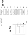
- FIG 13 shows a schematic view of a computing device 500 with which an FPGA design 502 formed using the method of the present invention may be used.
- the computing device 500 comprises a Central Processing Unit (CPU) 504, a main memory 506 and a data bus 508.
- CPU Central Processing Unit
- main memory 506 main memory
- data bus 508 data bus
- the CPU 504 may take any suitable form and comprises a processor for carrying out the instructions of a computer program run on the computing device 500.
- the CPU 504 is the primary element carrying out the functions of the computing device 500 as is well known in the art.
- the CPU 504 is commonly located on a motherboard (not shown) which comprises the necessary contacts to supply the CPU 504 with power and to connect the CPU 504 to other components in the computing device 500.
- the main memory 506 is associated with the CPU 504 and comprises an area of RAM.
- the RAM may take the form of SRAM, Dynamic RAM (DRAM) in which bits of data are stored as a charge in a capacitor or transistor gate, or any other suitable memory type.
- DRAM Dynamic RAM
- the main memory 506 may be provided as a plurality of SRAM or DRAM modules. These modules can quickly be replaced should they become damaged or when greater storage capacity is required.
- the main memory 506 is able to communicate with the CPU 504 via the motherboard forming part of the computing device 500.
- the data bus 508 enables additional devices to be connected to the computing device 500 and to communicate with components of the computing device 500.
- the data bus 508 may take any suitable form, for example a Peripheral Component Interconnect Express (PCI-E) data bus.
- PCI-E Peripheral Component Interconnect Express
- the data bus 508 acts as a motherboard-level interconnect to link motherboard-mounted peripherals and as an expansion card interface for add-in cards.
- the FPGA 502 is located on, in this example, an accelerator card 510.
- the accelerator card 510 is configured to connect to the data bus 508 and may be, for example, a PCI-E format expansion board comprising interconnects suitable for connecting to a PCI-E data bus.
- accelerator card 510 Whilst, for clarity, only a single accelerator card 510 is included in the following example, it would be readily apparent to the skilled person that additional accelerator cards comprising FPGAs 502 formed according to the method of the present invention may be included to provide additional computational power. For example, four accelerator cards 510 may be included in parallel within one system, with each card communicating to the CPU 504 and to each other. Alternatively, multiple FPGA devices 502 may be provided on a single accelerator card 510.
Landscapes
- Engineering & Computer Science (AREA)
- Theoretical Computer Science (AREA)
- Computer Hardware Design (AREA)
- Physics & Mathematics (AREA)
- General Engineering & Computer Science (AREA)
- General Physics & Mathematics (AREA)
- Software Systems (AREA)
- Evolutionary Computation (AREA)
- Geometry (AREA)
- Advance Control (AREA)
- Image Processing (AREA)
Claims (14)
- Verfahren zum Erzeugen eines Hardware-Designs für einen parallelen Stream-Prozessor mit Fließbandtechnik, wobei das Verfahren folgende Schritte umfasst:Definieren, an einer Computervorrichtung, eines Verarbeitungsvorgangs, der Prozesse bezeichnet, die in Hardware-Form als Teil des parallelen Stream-Prozessors mit Fließbandtechnik umzusetzen sind;Definieren, an einer Computervorrichtung, eines Graphen, der den Verarbeitungsvorgang als eine parallele Struktur in der Zeitdomäne als Funktion von Taktzyklen darstellt, wobei der Graph mindestens einen Datenweg, der als Hardware-Design für den parallelen Stream-Prozessor mit Fließbandtechnik umzusetzen ist, umfasst und eine Vielzahl von parallelen Zweigen, die konfiguriert sind, um über diese das Streamen von Datenwerten zu ermöglichen, umfasst, wobei der oder jeder Datenweg als mindestens einen Eingang, mindestens einen Ausgang, mindestens ein diskretes Objekt, das direkt einem Hardware-Element entspricht, das in Hardware-Form als Teil des parallelen Stream-Prozessors mit Fließbandtechnik umzusetzen ist, umfassend dargestellt ist, wobei das oder jedes diskrete Objekt betriebsfähig ist, um eine Funktion für einen oder mehrere Taktzyklen durchzuführen, und eine vordefinierte Latenz aufweist, die damit verknüpft ist, wobei die vordefinierte Latenz die Zeit darstellt, die das Hardware-Element benötigt, um die Funktion durchzuführen, wobei sich die Datenwerte über den Datenweg von dem mindestens einen Eingang zu dem mindestens einen Ausgang als Funktion eines zunehmenden Taktzyklus verbreiten;Definieren, an einer Computervorrichtung, des mindestens einen Datenwegs und der dazugehörigen Latenzen des Graphen als einen Satz von algebraischen linearen Ungleichheiten;gemeinsames Lösen, an einer Computervorrichtung, des Satzes von linearen Ungleichheiten für den gesamten Graphen;Optimieren, an einer Computervorrichtung, des mindestens einen Datenwegs in dem Graphen unter Verwendung der gelösten linearen Ungleichheiten, um einen optimierten Graphen zu erzeugen; undVerwenden, an einer Computervorrichtung, des optimierten Graphen, um ein optimiertes Hardware-Design zur Umsetzung in Hardware-Form als den parallelen Stream-Prozessor mit Fließbandtechnik zu definieren,wobei das Verfahren dadurch gekennzeichnet ist, dass der Schritt des Optimierens das Minimieren des Umfangs der Zwischenspeicherung, die benötigt wird, um den Datenweg einzuplanen und/oder des Einfügens einer Zwischenspeicherung in mindestens einige der Zweige des Datenwegs umfasst, und wobei der Schritt des Optimierens ferner das Zusammenlegen von zwei oder mehreren Zwischenspeichern in einen einzigen Zwischenspeicher und/oder das Zuteilen eines einzigen Zwischenspeichers zu einem oder mehreren Zweigen des mindestens einen Datenwegs umfasst.
- Verfahren nach Anspruch 1, wobei der Verarbeitungsvorgang eine mathematische Funktion oder Berechnung umfasst, der in Hardware-Form als der parallele Stream-Prozessor mit Fließbandtechnik umzusetzen ist.
- Verfahren nach Anspruch 1 oder 2, wobei das oder jedes Hardware-Element eine oder mehrere Hardware-Einheiten an dem parallelen Stream-Prozessor mit Fließbandtechnik umfasst und/oder konfiguriert ist, um eine vorbestimmte mathematische Funktion durchzuführen.
- Verfahren nach einem der Ansprüche 1 bis 3, wobei die Zwischenspeicherung Speichereinheiten an dem parallelen Stream-Prozessor mit Fließbandtechnik darstellt.
- Verfahren nach einem der Ansprüche 1 bis 4,wobei die Zwischenspeicherung für den gesamten Graphen minimiert ist.
- Verfahren nach einem der vorhergehenden Ansprüche, wobei der Graph mehrere Eingänge und mehrere Ausgänge umfasst, wobei jeder Eingang und jeder Ausgang an mindestens einen Zweig auf dem mindestens einen Datenweg angeschlossen ist.
- Verfahren nach Anspruch 6, wobei die Eingänge und/oder Ausgänge nicht zyklusausgerichtet sind.
- Verfahren nach einem der vorhergehenden Ansprüche, wobei der Graph mehrere parallele Datenwege umfasst, die in Hardware-Form als der parallele Stream-Prozessor mit Fließbandtechnik umzusetzen sind, und die Schritte des Lösens und Optimierens für jeden von den mehreren parallelen Datenwegen durchgeführt werden.
- Verfahren nach einem der vorhergehenden Ansprüche, ferner umfassend das Bereitstellen, an einer Computervorrichtung, mindestens eines Stream-Versatzobjekts, das sich an einem bestimmten Punkt auf dem Datenweg befindet, wobei das Stream-Versatzobjekt betriebsfähig ist, um für einen bestimmten Taktzyklus und für den bestimmten Punkt auf dem Datenweg auf Datenwerte von einem Taktzyklus, der anders als der bestimmte Taktzyklus ist, zuzugreifen.
- Verfahren nach einem der vorhergehenden Ansprüche, wobei der Stream-Prozessor als benutzerprogrammierbare Gatteranordnung oder als anwendungsspezifische integrierte Schaltung umgesetzt ist.
- Verfahren nach einem der vorhergehenden Ansprüche, ferner umfassend den Schritt des Bildens des optimierten Hardware-Designs an dem Stream-Prozessor, so dass der Stream-Prozessor betriebsfähig ist, um den Verarbeitungsvorgang auszuführen.
- Verfahren zum Herstellen einer programmierbaren Logikvorrichtung, umfassend folgende Schritte:Erzeugen eines Designs unter Verwendung des Verfahrens nach einem der Ansprüche 1 bis 9,Programmieren der Logikvorrichtung, um das erzeugte Design auszubilden.
- Computerprogramm, das eingerichtet ist, wenn es auf einem Computer abläuft, um die Schritte nach einem der vorhergehenden Ansprüche durchzuführen.
- Benutzerprogrammierbare Gatteranordnung, anwendungsspezifische integrierte Schaltung oder programmierbare Logikvorrichtung, die mit einem Hardware-Design konfiguriert ist, das unter Verwendung des Verfahrens nach einem der Ansprüche 1 bis 9 erzeugt wird.
Applications Claiming Priority (1)
| Application Number | Priority Date | Filing Date | Title |
|---|---|---|---|
| US13/029,696 US8464190B2 (en) | 2011-02-17 | 2011-02-17 | Method of, and apparatus for, stream scheduling in parallel pipelined hardware |
Publications (3)
| Publication Number | Publication Date |
|---|---|
| EP2490141A2 EP2490141A2 (de) | 2012-08-22 |
| EP2490141A3 EP2490141A3 (de) | 2012-12-19 |
| EP2490141B1 true EP2490141B1 (de) | 2019-06-12 |
Family
ID=45524278
Family Applications (1)
| Application Number | Title | Priority Date | Filing Date |
|---|---|---|---|
| EP11195864.1A Active EP2490141B1 (de) | 2011-02-17 | 2011-12-28 | Verfahren und Vorrichtung zur Planung von Befehlsströmen in einem parallelen Prozessor mit Befehls-Pipeline |
Country Status (4)
| Country | Link |
|---|---|
| US (2) | US8464190B2 (de) |
| EP (1) | EP2490141B1 (de) |
| JP (1) | JP6001873B2 (de) |
| GB (1) | GB2488195A (de) |
Families Citing this family (17)
| Publication number | Priority date | Publication date | Assignee | Title |
|---|---|---|---|---|
| CA2744746C (en) * | 2008-12-15 | 2019-12-24 | Exegy Incorporated | Method and apparatus for high-speed processing of financial market depth data |
| US8972923B2 (en) * | 2011-02-08 | 2015-03-03 | Maxeler Technologies Ltd. | Method and apparatus and software code for generating a hardware stream processor design |
| US9367658B2 (en) * | 2011-06-22 | 2016-06-14 | Maxeler Technologies Ltd. | Method and apparatus for designing and generating a stream processor |
| US20130046912A1 (en) * | 2011-08-18 | 2013-02-21 | Maxeler Technologies, Ltd. | Methods of monitoring operation of programmable logic |
| US8701069B1 (en) * | 2012-11-21 | 2014-04-15 | Maxeler Technologies, Ltd. | Systems and methods for optimizing allocation of hardware resources to control logic in parallel pipelined hardware |
| US8671371B1 (en) * | 2012-11-21 | 2014-03-11 | Maxeler Technologies Ltd. | Systems and methods for configuration of control logic in parallel pipelined hardware |
| US9146747B2 (en) | 2013-08-08 | 2015-09-29 | Linear Algebra Technologies Limited | Apparatus, systems, and methods for providing configurable computational imaging pipeline |
| US10001993B2 (en) | 2013-08-08 | 2018-06-19 | Linear Algebra Technologies Limited | Variable-length instruction buffer management |
| US11768689B2 (en) | 2013-08-08 | 2023-09-26 | Movidius Limited | Apparatus, systems, and methods for low power computational imaging |
| US9910675B2 (en) | 2013-08-08 | 2018-03-06 | Linear Algebra Technologies Limited | Apparatus, systems, and methods for low power computational imaging |
| US9727113B2 (en) | 2013-08-08 | 2017-08-08 | Linear Algebra Technologies Limited | Low power computational imaging |
| WO2017154183A1 (ja) * | 2016-03-10 | 2017-09-14 | 三菱電機株式会社 | 高位合成装置、高位合成方法及び高位合成プログラム |
| US10460704B2 (en) | 2016-04-01 | 2019-10-29 | Movidius Limited | Systems and methods for head-mounted display adapted to human visual mechanism |
| US10152566B1 (en) * | 2016-09-27 | 2018-12-11 | Altera Corporation | Constraint based bit-stream compression in hardware for programmable devices |
| US9661052B1 (en) * | 2016-10-14 | 2017-05-23 | International Business Machines Corporation | Reconfiguring a streaming application to reduce latency mismatches |
| US10949947B2 (en) | 2017-12-29 | 2021-03-16 | Intel Corporation | Foveated image rendering for head-mounted display devices |
| US11301295B1 (en) * | 2019-05-23 | 2022-04-12 | Xilinx, Inc. | Implementing an application specified as a data flow graph in an array of data processing engines |
Family Cites Families (11)
| Publication number | Priority date | Publication date | Assignee | Title |
|---|---|---|---|---|
| JP2002123563A (ja) * | 2000-10-13 | 2002-04-26 | Nec Corp | コンパイル方法および合成装置ならびに記録媒体 |
| US7000213B2 (en) | 2001-01-26 | 2006-02-14 | Northwestern University | Method and apparatus for automatically generating hardware from algorithms described in MATLAB |
| US6934938B2 (en) | 2002-06-28 | 2005-08-23 | Motorola, Inc. | Method of programming linear graphs for streaming vector computation |
| US6941541B2 (en) | 2002-07-19 | 2005-09-06 | Hewlett-Packard Development Company, L.P. | Efficient pipelining of synthesized synchronous circuits |
| US7107199B2 (en) * | 2002-10-31 | 2006-09-12 | Hewlett-Packard Development Company, L.P. | Method and system for the design of pipelines of processors |
| US7478377B2 (en) | 2004-06-07 | 2009-01-13 | International Business Machines Corporation | SIMD code generation in the presence of optimized misaligned data reorganization |
| US7395531B2 (en) | 2004-06-07 | 2008-07-01 | International Business Machines Corporation | Framework for efficient code generation using loop peeling for SIMD loop code with multiple misaligned statements |
| US7305649B2 (en) | 2005-04-20 | 2007-12-04 | Motorola, Inc. | Automatic generation of a streaming processor circuit |
| JP2009512089A (ja) | 2005-10-18 | 2009-03-19 | マイトリオニクス エービー | データフローマシンにおけるデッドロックを回避するための方法 |
| US7454597B2 (en) * | 2007-01-02 | 2008-11-18 | International Business Machines Corporation | Computer processing system employing an instruction schedule cache |
| US7817655B1 (en) | 2008-10-30 | 2010-10-19 | Xilinx, Inc. | Determining sizes of FIFO buffers between functional blocks in an electronic circuit |
-
2011
- 2011-02-17 US US13/029,696 patent/US8464190B2/en active Active
- 2011-12-28 GB GB1122363.3A patent/GB2488195A/en not_active Withdrawn
- 2011-12-28 EP EP11195864.1A patent/EP2490141B1/de active Active
-
2012
- 2012-02-16 JP JP2012031618A patent/JP6001873B2/ja active Active
-
2013
- 2013-02-27 US US13/779,457 patent/US8689156B2/en active Active
Non-Patent Citations (1)
| Title |
|---|
| None * |
Also Published As
| Publication number | Publication date |
|---|---|
| US8689156B2 (en) | 2014-04-01 |
| EP2490141A2 (de) | 2012-08-22 |
| US20130173890A1 (en) | 2013-07-04 |
| US8464190B2 (en) | 2013-06-11 |
| GB201122363D0 (en) | 2012-02-01 |
| EP2490141A3 (de) | 2012-12-19 |
| US20120216019A1 (en) | 2012-08-23 |
| GB2488195A (en) | 2012-08-22 |
| JP6001873B2 (ja) | 2016-10-05 |
| JP2012174268A (ja) | 2012-09-10 |
Similar Documents
| Publication | Publication Date | Title |
|---|---|---|
| EP2490141B1 (de) | Verfahren und Vorrichtung zur Planung von Befehlsströmen in einem parallelen Prozessor mit Befehls-Pipeline | |
| Page et al. | Compiling Occam into field-programmable gate arrays | |
| US8739101B1 (en) | Systems and methods for reducing logic switching noise in parallel pipelined hardware | |
| US8671371B1 (en) | Systems and methods for configuration of control logic in parallel pipelined hardware | |
| US8701069B1 (en) | Systems and methods for optimizing allocation of hardware resources to control logic in parallel pipelined hardware | |
| US8631380B2 (en) | Method of, and apparatus for, data path optimisation in parallel pipelined hardware | |
| JP2009524134A (ja) | ハードウェア定義方法 | |
| Liu et al. | Unified buffer: Compiling image processing and machine learning applications to push-memory accelerators | |
| Heyse et al. | Efficient implementation of virtual coarse grained reconfigurable arrays on FPGAs | |
| Arora et al. | Tensor slices: FPGA building blocks for the deep learning era | |
| Xydis et al. | High performance and area efficient flexible DSP datapath synthesis | |
| Akbari et al. | Toward approximate computing for coarse-grained reconfigurable architectures | |
| Dutta et al. | A holistic approach for tightly coupled reconfigurable parallel processors | |
| Rákossy et al. | Exploiting architecture description language for diverse IP synthesis in heterogeneous MPSoC | |
| Rykunov | Design of asynchronous microprocessor for power proportionality | |
| Wijtvliet et al. | Blocks, towards energy-efficient, coarse-grained reconfigurable architectures | |
| McAllister | Fpga-based dsp | |
| Ayala-Rincón et al. | Prototyping time-and space-efficient computations of algebraic operations over dynamically reconfigurable systems modeled by rewriting-logic | |
| Mehdipour et al. | A design scheme for a reconfigurable accelerator implemented by single-flux quantum circuits | |
| Gierenz et al. | Parameterized MAC unit generation for a scalable embedded DSP core | |
| Daigneault et al. | Fast description and synthesis of control-dominant circuits | |
| Chinnadurai et al. | Survey On Scheduling And Allocation In High Level Synthesis | |
| de Castro et al. | Finite-Time Lyapunov Exponent Calculation on FPGA using High-Level Synthesis Tools | |
| Toi et al. | High-level synthesis challenges for mapping a complete program on a dynamically reconfigurable processor | |
| Castro Caballero et al. | Finite-time lyapunov exponent calculation on FPGA using high-level synthesis tools |
Legal Events
| Date | Code | Title | Description |
|---|---|---|---|
| PUAI | Public reference made under article 153(3) epc to a published international application that has entered the european phase |
Free format text: ORIGINAL CODE: 0009012 |
|
| AK | Designated contracting states |
Kind code of ref document: A2 Designated state(s): AL AT BE BG CH CY CZ DE DK EE ES FI FR GB GR HR HU IE IS IT LI LT LU LV MC MK MT NL NO PL PT RO RS SE SI SK SM TR |
|
| AX | Request for extension of the european patent |
Extension state: BA ME |
|
| PUAL | Search report despatched |
Free format text: ORIGINAL CODE: 0009013 |
|
| AK | Designated contracting states |
Kind code of ref document: A3 Designated state(s): AL AT BE BG CH CY CZ DE DK EE ES FI FR GB GR HR HU IE IS IT LI LT LU LV MC MK MT NL NO PL PT RO RS SE SI SK SM TR |
|
| AX | Request for extension of the european patent |
Extension state: BA ME |
|
| RIC1 | Information provided on ipc code assigned before grant |
Ipc: G06F 17/50 20060101AFI20121109BHEP |
|
| 17P | Request for examination filed |
Effective date: 20130605 |
|
| RBV | Designated contracting states (corrected) |
Designated state(s): AL AT BE BG CH CY CZ DE DK EE ES FI FR GB GR HR HU IE IS IT LI LT LU LV MC MK MT NL NO PL PT RO RS SE SI SK SM TR |
|
| 17Q | First examination report despatched |
Effective date: 20160622 |
|
| STAA | Information on the status of an ep patent application or granted ep patent |
Free format text: STATUS: EXAMINATION IS IN PROGRESS |
|
| GRAP | Despatch of communication of intention to grant a patent |
Free format text: ORIGINAL CODE: EPIDOSNIGR1 |
|
| STAA | Information on the status of an ep patent application or granted ep patent |
Free format text: STATUS: GRANT OF PATENT IS INTENDED |
|
| INTG | Intention to grant announced |
Effective date: 20190307 |
|
| GRAS | Grant fee paid |
Free format text: ORIGINAL CODE: EPIDOSNIGR3 |
|
| GRAA | (expected) grant |
Free format text: ORIGINAL CODE: 0009210 |
|
| STAA | Information on the status of an ep patent application or granted ep patent |
Free format text: STATUS: THE PATENT HAS BEEN GRANTED |
|
| AK | Designated contracting states |
Kind code of ref document: B1 Designated state(s): AL AT BE BG CH CY CZ DE DK EE ES FI FR GB GR HR HU IE IS IT LI LT LU LV MC MK MT NL NO PL PT RO RS SE SI SK SM TR |
|
| REG | Reference to a national code |
Ref country code: GB Ref legal event code: FG4D |
|
| REG | Reference to a national code |
Ref country code: CH Ref legal event code: EP |
|
| REG | Reference to a national code |
Ref country code: AT Ref legal event code: REF Ref document number: 1143506 Country of ref document: AT Kind code of ref document: T Effective date: 20190615 |
|
| REG | Reference to a national code |
Ref country code: DE Ref legal event code: R096 Ref document number: 602011059590 Country of ref document: DE |
|
| REG | Reference to a national code |
Ref country code: IE Ref legal event code: FG4D |
|
| REG | Reference to a national code |
Ref country code: NL Ref legal event code: FP |
|
| REG | Reference to a national code |
Ref country code: LT Ref legal event code: MG4D |
|
| PG25 | Lapsed in a contracting state [announced via postgrant information from national office to epo] |
Ref country code: LT Free format text: LAPSE BECAUSE OF FAILURE TO SUBMIT A TRANSLATION OF THE DESCRIPTION OR TO PAY THE FEE WITHIN THE PRESCRIBED TIME-LIMIT Effective date: 20190612 Ref country code: ES Free format text: LAPSE BECAUSE OF FAILURE TO SUBMIT A TRANSLATION OF THE DESCRIPTION OR TO PAY THE FEE WITHIN THE PRESCRIBED TIME-LIMIT Effective date: 20190612 Ref country code: SE Free format text: LAPSE BECAUSE OF FAILURE TO SUBMIT A TRANSLATION OF THE DESCRIPTION OR TO PAY THE FEE WITHIN THE PRESCRIBED TIME-LIMIT Effective date: 20190612 Ref country code: HR Free format text: LAPSE BECAUSE OF FAILURE TO SUBMIT A TRANSLATION OF THE DESCRIPTION OR TO PAY THE FEE WITHIN THE PRESCRIBED TIME-LIMIT Effective date: 20190612 Ref country code: FI Free format text: LAPSE BECAUSE OF FAILURE TO SUBMIT A TRANSLATION OF THE DESCRIPTION OR TO PAY THE FEE WITHIN THE PRESCRIBED TIME-LIMIT Effective date: 20190612 Ref country code: NO Free format text: LAPSE BECAUSE OF FAILURE TO SUBMIT A TRANSLATION OF THE DESCRIPTION OR TO PAY THE FEE WITHIN THE PRESCRIBED TIME-LIMIT Effective date: 20190912 Ref country code: AL Free format text: LAPSE BECAUSE OF FAILURE TO SUBMIT A TRANSLATION OF THE DESCRIPTION OR TO PAY THE FEE WITHIN THE PRESCRIBED TIME-LIMIT Effective date: 20190612 |
|
| REG | Reference to a national code |
Ref country code: DE Ref legal event code: R079 Ref document number: 602011059590 Country of ref document: DE Free format text: PREVIOUS MAIN CLASS: G06F0017500000 Ipc: G06F0030000000 |
|
| PG25 | Lapsed in a contracting state [announced via postgrant information from national office to epo] |
Ref country code: LV Free format text: LAPSE BECAUSE OF FAILURE TO SUBMIT A TRANSLATION OF THE DESCRIPTION OR TO PAY THE FEE WITHIN THE PRESCRIBED TIME-LIMIT Effective date: 20190612 Ref country code: GR Free format text: LAPSE BECAUSE OF FAILURE TO SUBMIT A TRANSLATION OF THE DESCRIPTION OR TO PAY THE FEE WITHIN THE PRESCRIBED TIME-LIMIT Effective date: 20190913 Ref country code: BG Free format text: LAPSE BECAUSE OF FAILURE TO SUBMIT A TRANSLATION OF THE DESCRIPTION OR TO PAY THE FEE WITHIN THE PRESCRIBED TIME-LIMIT Effective date: 20190912 Ref country code: RS Free format text: LAPSE BECAUSE OF FAILURE TO SUBMIT A TRANSLATION OF THE DESCRIPTION OR TO PAY THE FEE WITHIN THE PRESCRIBED TIME-LIMIT Effective date: 20190612 |
|
| REG | Reference to a national code |
Ref country code: AT Ref legal event code: MK05 Ref document number: 1143506 Country of ref document: AT Kind code of ref document: T Effective date: 20190612 |
|
| PG25 | Lapsed in a contracting state [announced via postgrant information from national office to epo] |
Ref country code: CZ Free format text: LAPSE BECAUSE OF FAILURE TO SUBMIT A TRANSLATION OF THE DESCRIPTION OR TO PAY THE FEE WITHIN THE PRESCRIBED TIME-LIMIT Effective date: 20190612 Ref country code: RO Free format text: LAPSE BECAUSE OF FAILURE TO SUBMIT A TRANSLATION OF THE DESCRIPTION OR TO PAY THE FEE WITHIN THE PRESCRIBED TIME-LIMIT Effective date: 20190612 Ref country code: SK Free format text: LAPSE BECAUSE OF FAILURE TO SUBMIT A TRANSLATION OF THE DESCRIPTION OR TO PAY THE FEE WITHIN THE PRESCRIBED TIME-LIMIT Effective date: 20190612 Ref country code: PT Free format text: LAPSE BECAUSE OF FAILURE TO SUBMIT A TRANSLATION OF THE DESCRIPTION OR TO PAY THE FEE WITHIN THE PRESCRIBED TIME-LIMIT Effective date: 20191014 Ref country code: AT Free format text: LAPSE BECAUSE OF FAILURE TO SUBMIT A TRANSLATION OF THE DESCRIPTION OR TO PAY THE FEE WITHIN THE PRESCRIBED TIME-LIMIT Effective date: 20190612 Ref country code: EE Free format text: LAPSE BECAUSE OF FAILURE TO SUBMIT A TRANSLATION OF THE DESCRIPTION OR TO PAY THE FEE WITHIN THE PRESCRIBED TIME-LIMIT Effective date: 20190612 |
|
| PG25 | Lapsed in a contracting state [announced via postgrant information from national office to epo] |
Ref country code: IT Free format text: LAPSE BECAUSE OF FAILURE TO SUBMIT A TRANSLATION OF THE DESCRIPTION OR TO PAY THE FEE WITHIN THE PRESCRIBED TIME-LIMIT Effective date: 20190612 Ref country code: IS Free format text: LAPSE BECAUSE OF FAILURE TO SUBMIT A TRANSLATION OF THE DESCRIPTION OR TO PAY THE FEE WITHIN THE PRESCRIBED TIME-LIMIT Effective date: 20191012 Ref country code: SM Free format text: LAPSE BECAUSE OF FAILURE TO SUBMIT A TRANSLATION OF THE DESCRIPTION OR TO PAY THE FEE WITHIN THE PRESCRIBED TIME-LIMIT Effective date: 20190612 |
|
| REG | Reference to a national code |
Ref country code: DE Ref legal event code: R097 Ref document number: 602011059590 Country of ref document: DE |
|
| PG25 | Lapsed in a contracting state [announced via postgrant information from national office to epo] |
Ref country code: TR Free format text: LAPSE BECAUSE OF FAILURE TO SUBMIT A TRANSLATION OF THE DESCRIPTION OR TO PAY THE FEE WITHIN THE PRESCRIBED TIME-LIMIT Effective date: 20190612 |
|
| PLBE | No opposition filed within time limit |
Free format text: ORIGINAL CODE: 0009261 |
|
| STAA | Information on the status of an ep patent application or granted ep patent |
Free format text: STATUS: NO OPPOSITION FILED WITHIN TIME LIMIT |
|
| PG25 | Lapsed in a contracting state [announced via postgrant information from national office to epo] |
Ref country code: DK Free format text: LAPSE BECAUSE OF FAILURE TO SUBMIT A TRANSLATION OF THE DESCRIPTION OR TO PAY THE FEE WITHIN THE PRESCRIBED TIME-LIMIT Effective date: 20190612 Ref country code: PL Free format text: LAPSE BECAUSE OF FAILURE TO SUBMIT A TRANSLATION OF THE DESCRIPTION OR TO PAY THE FEE WITHIN THE PRESCRIBED TIME-LIMIT Effective date: 20190612 |
|
| 26N | No opposition filed |
Effective date: 20200313 |
|
| PG25 | Lapsed in a contracting state [announced via postgrant information from national office to epo] |
Ref country code: SI Free format text: LAPSE BECAUSE OF FAILURE TO SUBMIT A TRANSLATION OF THE DESCRIPTION OR TO PAY THE FEE WITHIN THE PRESCRIBED TIME-LIMIT Effective date: 20190612 Ref country code: IS Free format text: LAPSE BECAUSE OF FAILURE TO SUBMIT A TRANSLATION OF THE DESCRIPTION OR TO PAY THE FEE WITHIN THE PRESCRIBED TIME-LIMIT Effective date: 20200224 |
|
| PG2D | Information on lapse in contracting state deleted |
Ref country code: IS |
|
| REG | Reference to a national code |
Ref country code: BE Ref legal event code: MM Effective date: 20191231 |
|
| PG25 | Lapsed in a contracting state [announced via postgrant information from national office to epo] |
Ref country code: MC Free format text: LAPSE BECAUSE OF FAILURE TO SUBMIT A TRANSLATION OF THE DESCRIPTION OR TO PAY THE FEE WITHIN THE PRESCRIBED TIME-LIMIT Effective date: 20190612 |
|
| PG25 | Lapsed in a contracting state [announced via postgrant information from national office to epo] |
Ref country code: LU Free format text: LAPSE BECAUSE OF NON-PAYMENT OF DUE FEES Effective date: 20191228 Ref country code: IE Free format text: LAPSE BECAUSE OF NON-PAYMENT OF DUE FEES Effective date: 20191228 |
|
| PG25 | Lapsed in a contracting state [announced via postgrant information from national office to epo] |
Ref country code: BE Free format text: LAPSE BECAUSE OF NON-PAYMENT OF DUE FEES Effective date: 20191231 |
|
| PG25 | Lapsed in a contracting state [announced via postgrant information from national office to epo] |
Ref country code: CY Free format text: LAPSE BECAUSE OF FAILURE TO SUBMIT A TRANSLATION OF THE DESCRIPTION OR TO PAY THE FEE WITHIN THE PRESCRIBED TIME-LIMIT Effective date: 20190612 |
|
| PG25 | Lapsed in a contracting state [announced via postgrant information from national office to epo] |
Ref country code: MT Free format text: LAPSE BECAUSE OF FAILURE TO SUBMIT A TRANSLATION OF THE DESCRIPTION OR TO PAY THE FEE WITHIN THE PRESCRIBED TIME-LIMIT Effective date: 20190612 Ref country code: HU Free format text: LAPSE BECAUSE OF FAILURE TO SUBMIT A TRANSLATION OF THE DESCRIPTION OR TO PAY THE FEE WITHIN THE PRESCRIBED TIME-LIMIT; INVALID AB INITIO Effective date: 20111228 |
|
| PG25 | Lapsed in a contracting state [announced via postgrant information from national office to epo] |
Ref country code: MK Free format text: LAPSE BECAUSE OF FAILURE TO SUBMIT A TRANSLATION OF THE DESCRIPTION OR TO PAY THE FEE WITHIN THE PRESCRIBED TIME-LIMIT Effective date: 20190612 |
|
| P01 | Opt-out of the competence of the unified patent court (upc) registered |
Effective date: 20240110 |
|
| PGFP | Annual fee paid to national office [announced via postgrant information from national office to epo] |
Ref country code: CH Payment date: 20250101 Year of fee payment: 14 |
|
| REG | Reference to a national code |
Ref country code: DE Ref legal event code: R081 Ref document number: 602011059590 Country of ref document: DE Owner name: GROQ UK LTD., GB Free format text: FORMER OWNER: MAXELER TECHNOLOGIES LTD., LONDON, GB Ref country code: DE Ref legal event code: R082 Ref document number: 602011059590 Country of ref document: DE |
|
| REG | Reference to a national code |
Ref country code: NL Ref legal event code: HC Owner name: GROQ UK LIMITED; GB Free format text: DETAILS ASSIGNMENT: CHANGE OF OWNER(S), CHANGE OF OWNER(S) NAME; FORMER OWNER NAME: MAXELER TECHNOLOGIES LTD. Effective date: 20250916 |
|
| REG | Reference to a national code |
Ref country code: CH Ref legal event code: R18 Free format text: ST27 STATUS EVENT CODE: U-0-0-R10-R18 (AS PROVIDED BY THE NATIONAL OFFICE) Effective date: 20251020 |
|
| REG | Reference to a national code |
Ref country code: CH Ref legal event code: U11 Free format text: ST27 STATUS EVENT CODE: U-0-0-U10-U11 (AS PROVIDED BY THE NATIONAL OFFICE) Effective date: 20260101 |
|
| PGFP | Annual fee paid to national office [announced via postgrant information from national office to epo] |
Ref country code: DE Payment date: 20251209 Year of fee payment: 15 |
|
| PGFP | Annual fee paid to national office [announced via postgrant information from national office to epo] |
Ref country code: GB Payment date: 20251210 Year of fee payment: 15 |
|
| PGFP | Annual fee paid to national office [announced via postgrant information from national office to epo] |
Ref country code: NL Payment date: 20251210 Year of fee payment: 15 Ref country code: FR Payment date: 20251210 Year of fee payment: 15 |