EP2489078B1 - Power inverter docking system for photovoltaic modules - Google Patents
Power inverter docking system for photovoltaic modules Download PDFInfo
- Publication number
- EP2489078B1 EP2489078B1 EP10771599.7A EP10771599A EP2489078B1 EP 2489078 B1 EP2489078 B1 EP 2489078B1 EP 10771599 A EP10771599 A EP 10771599A EP 2489078 B1 EP2489078 B1 EP 2489078B1
- Authority
- EP
- European Patent Office
- Prior art keywords
- docking
- connector port
- inverter
- photovoltaic module
- module
- Prior art date
- Legal status (The legal status is an assumption and is not a legal conclusion. Google has not performed a legal analysis and makes no representation as to the accuracy of the status listed.)
- Not-in-force
Links
- 238000003032 molecular docking Methods 0.000 title claims description 138
- 230000008878 coupling Effects 0.000 claims description 21
- 238000010168 coupling process Methods 0.000 claims description 21
- 238000005859 coupling reaction Methods 0.000 claims description 21
- 238000000034 method Methods 0.000 claims description 8
- 239000004020 conductor Substances 0.000 description 18
- 238000010586 diagram Methods 0.000 description 4
- 239000000853 adhesive Substances 0.000 description 2
- 230000001070 adhesive effect Effects 0.000 description 2
- 230000007246 mechanism Effects 0.000 description 2
- 230000000284 resting effect Effects 0.000 description 2
- 238000005476 soldering Methods 0.000 description 2
- 239000002131 composite material Substances 0.000 description 1
- 238000002788 crimping Methods 0.000 description 1
- 239000002184 metal Substances 0.000 description 1
- 239000011347 resin Substances 0.000 description 1
- 229920005989 resin Polymers 0.000 description 1
Images


Classifications
-
- H—ELECTRICITY
- H01—ELECTRIC ELEMENTS
- H01L—SEMICONDUCTOR DEVICES NOT COVERED BY CLASS H10
- H01L31/00—Semiconductor devices sensitive to infrared radiation, light, electromagnetic radiation of shorter wavelength or corpuscular radiation and specially adapted either for the conversion of the energy of such radiation into electrical energy or for the control of electrical energy by such radiation; Processes or apparatus specially adapted for the manufacture or treatment thereof or of parts thereof; Details thereof
- H01L31/04—Semiconductor devices sensitive to infrared radiation, light, electromagnetic radiation of shorter wavelength or corpuscular radiation and specially adapted either for the conversion of the energy of such radiation into electrical energy or for the control of electrical energy by such radiation; Processes or apparatus specially adapted for the manufacture or treatment thereof or of parts thereof; Details thereof adapted as photovoltaic [PV] conversion devices
- H01L31/042—PV modules or arrays of single PV cells
- H01L31/048—Encapsulation of modules
-
- H—ELECTRICITY
- H01—ELECTRIC ELEMENTS
- H01L—SEMICONDUCTOR DEVICES NOT COVERED BY CLASS H10
- H01L31/00—Semiconductor devices sensitive to infrared radiation, light, electromagnetic radiation of shorter wavelength or corpuscular radiation and specially adapted either for the conversion of the energy of such radiation into electrical energy or for the control of electrical energy by such radiation; Processes or apparatus specially adapted for the manufacture or treatment thereof or of parts thereof; Details thereof
- H01L31/02—Details
- H01L31/02002—Arrangements for conducting electric current to or from the device in operations
- H01L31/02005—Arrangements for conducting electric current to or from the device in operations for device characterised by at least one potential jump barrier or surface barrier
- H01L31/02008—Arrangements for conducting electric current to or from the device in operations for device characterised by at least one potential jump barrier or surface barrier for solar cells or solar cell modules
- H01L31/0201—Arrangements for conducting electric current to or from the device in operations for device characterised by at least one potential jump barrier or surface barrier for solar cells or solar cell modules comprising specially adapted module bus-bar structures
-
- H—ELECTRICITY
- H01—ELECTRIC ELEMENTS
- H01R—ELECTRICALLY-CONDUCTIVE CONNECTIONS; STRUCTURAL ASSOCIATIONS OF A PLURALITY OF MUTUALLY-INSULATED ELECTRICAL CONNECTING ELEMENTS; COUPLING DEVICES; CURRENT COLLECTORS
- H01R13/00—Details of coupling devices of the kinds covered by groups H01R12/70 or H01R24/00 - H01R33/00
- H01R13/62—Means for facilitating engagement or disengagement of coupling parts or for holding them in engagement
- H01R13/629—Additional means for facilitating engagement or disengagement of coupling parts, e.g. aligning or guiding means, levers, gas pressure electrical locking indicators, manufacturing tolerances
- H01R13/631—Additional means for facilitating engagement or disengagement of coupling parts, e.g. aligning or guiding means, levers, gas pressure electrical locking indicators, manufacturing tolerances for engagement only
-
- H—ELECTRICITY
- H01—ELECTRIC ELEMENTS
- H01R—ELECTRICALLY-CONDUCTIVE CONNECTIONS; STRUCTURAL ASSOCIATIONS OF A PLURALITY OF MUTUALLY-INSULATED ELECTRICAL CONNECTING ELEMENTS; COUPLING DEVICES; CURRENT COLLECTORS
- H01R13/00—Details of coupling devices of the kinds covered by groups H01R12/70 or H01R24/00 - H01R33/00
- H01R13/73—Means for mounting coupling parts to apparatus or structures, e.g. to a wall
-
- H—ELECTRICITY
- H02—GENERATION; CONVERSION OR DISTRIBUTION OF ELECTRIC POWER
- H02M—APPARATUS FOR CONVERSION BETWEEN AC AND AC, BETWEEN AC AND DC, OR BETWEEN DC AND DC, AND FOR USE WITH MAINS OR SIMILAR POWER SUPPLY SYSTEMS; CONVERSION OF DC OR AC INPUT POWER INTO SURGE OUTPUT POWER; CONTROL OR REGULATION THEREOF
- H02M7/00—Conversion of ac power input into dc power output; Conversion of dc power input into ac power output
- H02M7/42—Conversion of dc power input into ac power output without possibility of reversal
- H02M7/44—Conversion of dc power input into ac power output without possibility of reversal by static converters
-
- H—ELECTRICITY
- H02—GENERATION; CONVERSION OR DISTRIBUTION OF ELECTRIC POWER
- H02S—GENERATION OF ELECTRIC POWER BY CONVERSION OF INFRARED RADIATION, VISIBLE LIGHT OR ULTRAVIOLET LIGHT, e.g. USING PHOTOVOLTAIC [PV] MODULES
- H02S40/00—Components or accessories in combination with PV modules, not provided for in groups H02S10/00 - H02S30/00
- H02S40/30—Electrical components
- H02S40/32—Electrical components comprising DC/AC inverter means associated with the PV module itself, e.g. AC modules
-
- H—ELECTRICITY
- H02—GENERATION; CONVERSION OR DISTRIBUTION OF ELECTRIC POWER
- H02S—GENERATION OF ELECTRIC POWER BY CONVERSION OF INFRARED RADIATION, VISIBLE LIGHT OR ULTRAVIOLET LIGHT, e.g. USING PHOTOVOLTAIC [PV] MODULES
- H02S40/00—Components or accessories in combination with PV modules, not provided for in groups H02S10/00 - H02S30/00
- H02S40/30—Electrical components
- H02S40/34—Electrical components comprising specially adapted electrical connection means to be structurally associated with the PV module, e.g. junction boxes
-
- H—ELECTRICITY
- H05—ELECTRIC TECHNIQUES NOT OTHERWISE PROVIDED FOR
- H05K—PRINTED CIRCUITS; CASINGS OR CONSTRUCTIONAL DETAILS OF ELECTRIC APPARATUS; MANUFACTURE OF ASSEMBLAGES OF ELECTRICAL COMPONENTS
- H05K7/00—Constructional details common to different types of electric apparatus
- H05K7/02—Arrangements of circuit components or wiring on supporting structure
- H05K7/10—Plug-in assemblages of components, e.g. IC sockets
-
- Y—GENERAL TAGGING OF NEW TECHNOLOGICAL DEVELOPMENTS; GENERAL TAGGING OF CROSS-SECTIONAL TECHNOLOGIES SPANNING OVER SEVERAL SECTIONS OF THE IPC; TECHNICAL SUBJECTS COVERED BY FORMER USPC CROSS-REFERENCE ART COLLECTIONS [XRACs] AND DIGESTS
- Y02—TECHNOLOGIES OR APPLICATIONS FOR MITIGATION OR ADAPTATION AGAINST CLIMATE CHANGE
- Y02E—REDUCTION OF GREENHOUSE GAS [GHG] EMISSIONS, RELATED TO ENERGY GENERATION, TRANSMISSION OR DISTRIBUTION
- Y02E10/00—Energy generation through renewable energy sources
- Y02E10/50—Photovoltaic [PV] energy
- Y02E10/56—Power conversion systems, e.g. maximum power point trackers
-
- Y—GENERAL TAGGING OF NEW TECHNOLOGICAL DEVELOPMENTS; GENERAL TAGGING OF CROSS-SECTIONAL TECHNOLOGIES SPANNING OVER SEVERAL SECTIONS OF THE IPC; TECHNICAL SUBJECTS COVERED BY FORMER USPC CROSS-REFERENCE ART COLLECTIONS [XRACs] AND DIGESTS
- Y10—TECHNICAL SUBJECTS COVERED BY FORMER USPC
- Y10T—TECHNICAL SUBJECTS COVERED BY FORMER US CLASSIFICATION
- Y10T29/00—Metal working
- Y10T29/49—Method of mechanical manufacture
- Y10T29/49002—Electrical device making
Definitions
- This invention relates to power electronic docking systems, and more specifically to power inverter docking systems for photovoltaic modules.
- PV modules may generate direct current (DC) power based on received solar energy.
- PV modules may include a plurality of PV cells electrically coupled to one another allowing the cells to contribute to a combined output power for a PV module.
- the DC power generated by a photovoltaic module may be converted to AC power through the use of a power inverter.
- the power inverter may be electrically coupled to an output of the PV module.
- intervening wiring may be used between the PV module and the power inverter.
- the power inverter may be directly connected to wires included in the intervening wiring.
- the power inverter may be located physically apart from the PV module, with only the intervening wiring and associated hardware physically coupling the PV module to the power inverter.
- EP 0 793 278 A2 describes a photo-voltaic apparatus comprising a photo-voltaic module having a plurality of photo-voltaic cells, and an inverter for converting a direct current output generated from the photo-voltaic cells into an alternating current and outputting the alternating current, the inverter being mounted on a surface opposite to the light receiving surface of the photo-voltaic module with a clearance provided therebetween.
- a power inverter docking system for a photovoltaic module.
- the power inverter docking system includes a junction box that includes a first connector port configured to be electrically coupled to at least one photovoltaic cell of the photovoltaic module.
- the power inverter docking system also includes a docking member configured to be coupled to the photovoltaic module.
- the docking member is configured to be removably coupled to the first connector port.
- the docking member includes at least one junction box slot configured to allow the junction box to be coupled to the docking member.
- the power inverter docking system further includes an inverter housing configured to be removably coupled to the photovoltaic module and configured to at least partially house a power inverter, the inverter housing including a second connector port electrically coupled to the power inverter.
- the second connector port is configured to be selectively engageable to the first connector port and to be removably coupled to the photovoltaic module.
- the docking member may be configured to be removably coupled to the photovoltaic module.
- the inverter housing may be removably coupled to the docking member to secure the inverter housing with respect to the PV module.
- the power inverter may convert direct current (DC) power generated by the PV module to alternating current (AC) power for various AC power applications.
- a photovoltaic module comprising at least one photovoltaic cell, and a docking system.
- the docking system includes a junction box that includes a first connector port configured to be electrically coupled to the at least one photovoltaic cell.
- the docking system also includes a docking member configured to be coupled to the photovoltaic module and comprising at least one junction box slot configured to allow the junction box to be coupled to the docking member.
- the docking system further includes a housing configured to enclose at least a portion of a power electronics module.
- the housing includes a second connector port configured to be electrically coupled to the power electronics module.
- the second connector port is configured to removably engage the first connector port.
- the power electronics module and the at least one photovoltaic cell are electrically coupled to one another when the second connector port is removably engaged to the first connector port.
- the housing is configured to be removably coupled to the photovoltaic module.
- a method of assembling a docking system for a photovoltaic module includes coupling a docking member to the photovoltaic module.
- the method also includes electrically coupling a first connector port of a junction box to at least one photovoltaic cell of the photovoltaic module.
- the method further includes coupling the junction box to the docking member.
- the method also includes electrically coupling the first connector port with a second connector port, in which the second connector port is electrically coupled to a power electronics module enclosed within a housing.
- the method further includes removably coupling the housing to the photovoltaic module.
- a docking system may be implemented for a photovoltaic module.
- the docking system may include docking member removably coupled to or integrally formed with a photovoltaic module.
- the docking system may also include a photovoltaic connector port electrically coupled to photovoltaic cells of the photovoltaic module.
- the photovoltaic module may be selectively coupled to the docking member.
- the docking system may also include a housing to enclose a power electronics module, such as a power inverter or converter.
- the housing may include an inverter housing connector port that is selectively engageable to the power electronics module.
- the power electronics module and the photovoltaic cells may be electrically coupled to one another upon selective engagement of the connector ports.
- the inverter housing may be received by and removably coupled to the docking member allowing the inverter housing to be removably coupled to the photovoltaic module.
- FIG. 1 is a perspective view of a photovoltaic module (PV) module 100.
- the PV module 100 may include a plurality of PV cells 102 disposed within a frame 104 of the PV module 100.
- the PV cells 102 may be electrically coupled in various configurations, such as sub-groups of PV cells 102 for example.
- the PV cells 102 may be configured to be exposed along a top surface 106 of the PV module 100 allowing the PV cells 102 to receive solar energy and convert the solar energy into electric power.
- the electric power produced by the PV cells 102 is direct-current (DC) based.
- the DC power from the PV cells 102 may be converted to alternating current (AC) power for use in AC power applications such as distribution portions of utility power grids.
- AC alternating current
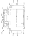
- FIG. 2 is a perspective view of an underside of the photovoltaic (PV) module 100.
- a docking system 200 may include an inverter housing 202 removably coupled to the PV module 100.
- the inverter housing 202 may enclose a power inverter 203, conceptually represented in phantom in FIG. 2 .
- the inverter housing 202 may be formed of an inverter housing cover 205 and an inverter housing enclosure 207 removably coupled to one another by a plurality of fasteners 209.
- the fasteners 209 may be threaded fasteners such as screws or bolts.
- the power inverter 203 may be electrically coupled to the PV cells 102 of the PV module 100.
- the power inverter 203 such as a DC link inverter, AC link inverter, transformerless inverter, or any other suitable inverter topology.
- the power inverter 203 may provide a single-phase or a three-phase output.
- the inverter 203 topology may be constructed with multiple power stages, one of which may be an active filter converter.
- the inverter housing 202 may be used to enclose one or more power inverters 203 or other power converter modules, such as DC-DC power converters, that may be electrically coupled to the PV module 100 for various applications.
- one or more power converters may be electrically coupled to the PV module 100 and the power inverter 203.
- a junction box 204 may provide electrical access to the PV cells 102 of the PV module 100 to the power inverter 203.
- the junction box 204 may be electrically coupled to the power inverter 203 enclosed within the inverter housing 202, allowing DC power generated by the PV module 100 to be converted to AC power and transmitted through a plurality of electrical conductors ( FIG. 7 ) electrically coupled to the power inverter 203.
- the conductors may be disposed within an electrical cable 206.
- the junction box 204 may be formed of a non-electrically-conductive material such as plastic, resin, or a composite material, for example. In other examples, the junction box 204 may be formed of an electrically-conductive material.
- a docking member 208 may be secured to the PV module 100.
- the docking member 208 may include a bracket 211 that may be removably coupled to a rail 210 of the PV module 100 through a plurality of fasteners 212.
- the rail 210 may be part of the frame 104.
- the bracket 211 may include a plurality of openings 213 to receive the fasteners 212.
- the fasteners 212 are illustrated as threaded fasteners, such as screws or bolts. However, various other fasteners, such as adhesives, clips, or other suitable coupling mechanisms may be used to removably couple the docking member 208 to the PV module 100.
- the docking member 208 may also be permanently or removably fastened to a surface 214 of the PV module 100 through the use of various suitable fastening manners such as fasteners, adhesives, or soldering, for example.
- the docking member 208 may be secured to the PV module 100 in a manner other than that shown in FIG. 2 .
- the docking member 208 may be configured to be secured to the PV module 100 without being secured to both the rail 210 and the surface 214 of the PV module.
- the docking member 208 may be integrally formed with the PV module 100, such as with the surface 214.
- the docking member 208 may be removably coupled to the inverter housing 202 and the junction box 204.
- the docking member 208 may include a first rail 216 and a second rail 218.
- the inverter housing 202 may be selectively received by the docking member 208 and the inverter housing 202 may be disposed between the rails 216, 218.
- the inverter housing 202 may be removably coupled to the docking member 208 through fasteners 220. Removable coupling allows the inverter housing 202 to be removed from the docking system 200 allowing repair, replacement, etc., of the inverter housing 202.
- the fasteners 220 may be captive threaded fasteners, such as captive screws or bolts.
- the fasteners 220 may also be any other suitable fasteners, such as clips, for example, allowing coupling.
- the docking member 208 may also include a first junction box slot 222 and a second junction box slot 224 ( FIG. 3 ) allowing the junction box 204 to be removably coupled to the docking member 208.
- the junction box 204 may include a first tab 225 ( FIG. 3 ) and a second tab 227 ( FIG. 5 ) that may disposed through a first opening 228 and a second opening 230 ( FIG. 3 ) of the slots 222, 224, respectively.
- the inverter housing 202 and docking member 208 may be formed of an electrically conductive material, such as a metal.
- the electrically-conductive material may assist with grounding of the inverter housing 202, which is in contact with the docking member 208.
- the docking member 208 may be in contact with the surface 214 of the PV module 100, which may also be formed of an electrically conductive material.
- a chain of contact such as this may provide grounding for the inverter housing 202.
- a grounding conductor (see FIG. 7 ) may also be provided to the inverter housing module 202 included in the cable 206 or external to the cable 206.
- the grounding cable may terminate within the inverter housing 202, which may also provide grounding to the docking member 208.
- FIG. 3 shows an exploded view of one example of the docking system 200 and PV module 100.
- the junction box 204 may include a cover 300 and an enclosure 302.
- the cover 300 may be removably coupled to the enclosure 302.
- the cover 300 of the junction box 204 may include a plurality of clip arms 304.
- Each clip arm 304 may extend from a body 306 of the cover 300.
- Each clip arm 304 may correspond to one of a plurality of cover receivers 308.
- each cover receiver 308 may be a ridge formed in the enclosure 302 for engagement with a corresponding clip arm 304.
- the cover 300 may be pressed onto the enclosure 302 causing each clip arm 304 to engage one of the cover receivers 308, such as being forced around each corresponding cover receiver 308 biasing each clip arm 304 from an initial respective resting position shown in FIG. 3 .
- Each clip arm 304 may be resilient allowing each clip arm 304 to attempt to return to the initial resting position causing the clip arms 304 to engage the corresponding cover receiver 308 to removably couple the cover 300 to the enclosure 302, as shown in FIG. 2 .
- Other suitable manners of removably coupling the cover 300 to the enclosure 302 may be implemented.
- the cover 300 may be coupled to the enclosure 302 through a hinge, allowing the cover 300 to pivot between an open and closed position allowing internal access to the enclosure 302.
- the enclosure 302 may include a first docking projection 310 and a second docking projection 312 ( FIG. 5 ). Each docking projection 310, 312 may slide within a corresponding slot 222, 224 of the docking member 208.
- the openings 228, 230 may each receive the respective tab 225, 227 on each of the projections 310, 312. Receipt of each tab 225, 227 may secure the enclosure 302 of the junction box 204 into place with respect to the docking member 208.
- the projections 310, 312 may be received by slots 222, 224, respectively, in a plane substantially parallel to the surface 214.
- the tabs 225, 227 may be received by the openings 228, 230, respectively, in a plane substantially perpendicular to the surface 214.
- the enclosure 302 may include an enclosure access opening 314, such as a slot, disposed through a surface 316 of the enclosure 302.
- the enclosure 302 may also include a PV connector port 318.
- the enclosure 302 may be positioned to align the enclosure access opening 314 with a PV module opening 320, such as a slot.
- the PV module opening 320 may be disposed in the surface 214 and allow access to connectors 322 of the PV module 100.
- the docking member 208 may include a PV access opening 323, such as a slot, that may be aligned with the enclosure access opening 314 and the PV module opening 320.
- the connectors 322 may be ribbon connectors electrically connected to the PV cells 102 of the PV module 100. However, other connectors, such as wires, may be implemented in the PV module 100 allowing electrical interfacing with the PV cells 102.
- the docking member 208 may include a junction box access opening 325 allowing for further internal access to the junction box 204
- the PV connector port 318 may be removably coupled to a n inverter housing connector port 324 of the inverter housing 202.
- the inverter housing connector port 318 may be selectively engaged and disengaged with the PV connector port 324 along a plane substantially parallel to the surface 214.
- the inverter housing connector port 324 may be electrically coupled with the power inverter 203. In other examples, the inverter housing connector port 324 may be included with the power inverter 203.
- the engagement of the connector ports 318, 324 allows power generated by the PV module 100 to be received by the power inverter 203.
- the docking member 208 may include a plurality of docking arms 326, each having a respective opening 328.
- the inverter housing 202 may include a plurality of docking tabs 330 extending outwardly from the inverter housing 202. In FIG. 3 , the docking tabs 330 the docking tabs extend outwardly from the inverter housing cover 205 of the inverter housing 202. However, in other examples, some or all of the docking tabs 330 may extend from the inverter housing enclosure 207. Each docking tab 330 may include a respective opening 332.
- the docking arms 326 and docking tabs 330 may be positioned such that the openings 328 of each docking arm 326 and the openings 332 of each docking tab 330 align when the connector ports 318, 324 are coupled to one another.
- the fasteners 220 may be disposed through the aligned openings 328, 332 to secure the inverter housing 202 to the docking member 208.
- the rails 216, 218 of the docking member 208 may assist in the physical alignment of the inverter housing connector port 324 with the PV connector port 318.
- FIG. 4 is another perspective view of the docking system 200 and the PV module 100.
- the inverter housing 202 may include a plate 400 coupled to the inverter housing enclosure 207 of the inverter housing 202 to which the cable 206 is coupled.
- FIG. 5 is a plan view of an example of the enclosure 302.
- the plan view illustrates an example placement and configuration of the docking projections 310, 312.
- the tabs 225, 227 are disposed along the projections 310, 312, respectively.
- the tabs 225, 227 may be separately coupled to the projections, 310, 312, respectively, or may be integrally formed thereon.
- the PV connector port 318 may include a junction box connector plate 500 coupled to the enclosure 302 through one or more fasteners 502, such as screws, bolts, rivets, or other suitable fastener for removable or permanent coupling.
- the connector plate 500 may include a first guide post cavity 504 and second guide post cavity 505 formed within the connector plate 500.
- the guide post cavities 504, 505 may receive guide posts 700, 702 ( FIG.7 ) from the inverter housing connector port 324.
- the PV connector port 318 may also include a plurality of sockets 506.
- the sockets 506 may receive connector pins 704 ( FIG. 7 ) from the inverter housing connector port 324.
- Receipt of the connector pins 704 may result in electrical coupling between the power inverter 203 and the PV module 100 as described with regard to FIGS. 2 and 3 .
- the sockets 506 may be electrically coupled to a printed wiring board (PWB) 508.
- the PWB 508 may have a portion overlapping the PV connector port 318.
- the PWB 508 may be directly coupled to the sockets 506 or through intervening conductors (not shown).
- the PWB 508 may be electrically connected with the connectors 322 of the PV module 100 and may include conductors 800 (see FIG. 8 ) to electrically couple the connectors 322 to the sockets 506 on the PWB 508.
- FIG. 6 is a plan view of the enclosure 302 from an opposite view as that shown in FIG. 5 .
- the plan view of FIG. 6 illustrates cavities 600, 602 formed by the enclosure 302.
- a fastener receptacle 608, 610 are also disposed in each cavity 600, 602 that may be formed in the enclosure 302 to receive the fastener 502, respectively, to couple the connector plate 500 to the enclosure 302.
- the enclosure 302 may also include an opening 612 allowing access to a socket connector board 614.
- FIG. 7 is a plan view of the inverter housing 202.
- the inverter housing connector port 324 may include guide posts 700, 702. As discussed with regard to FIG. 5 , the guide posts 700, 702 may be formed to be received by the guide post cavities 504, 505, respectively, when the connector ports 318, 324 are connected to one another.
- the inverter housing connector port 324 may also include a plurality of connector pins 704.
- the connector pins 704 may be electrically coupled to a PWB 706 (shown conceptually in phantom) internal to the inverter housing 202.
- the power inverter 203 may be electrically coupled to the PWB 706.
- the power inverter 203 may include a plurality of circuit elements arranged to convert DC power from the PV module 100 to AC power transmitted through the conductors 710 within the cable 206.
- the conductor 712 may serve as a grounding conductor and be coupled to a fastener 209.
- the conductors 710, 712 within the cable 206 may be connected to a number of other PV modules, a utility power grid, a stand-alone AC power load, or some combination of thereof.
- the PV connector port 324 may include a connector plate 714 that includes the connector pins 704.
- the connector plate 714 may be removably coupled to the inverter housing 202 through one or more fasteners, such as fasteners 209 shown in FIG. 2 .
- FIG. 8 is a perspective view of an example of the inverter housing connector port 318 prior to connection with the PV connector port 324.
- FIG. 8 provides an internal view of the enclosure 302.
- the PWB 508 may provide a surface for the conductors 800 to span for connection with the sockets 506.
- the sockets 506 may be mounted to the socket mounting board 614.
- the conductors 800 may be the connectors 322 of the PV module 100 or may be intervening conductors between the connectors 322 and the sockets 506.
- the connections between the connectors 322 and the sockets 506 may be made in various manners, such as crimping, soldering, or other manner of connection allowing electrical coupling of the sockets 506 to the connectors 322.
- FIG. 8 also shows an example of the guide posts 700, 702 being connected to the inverter housing connector port 324 through fasteners 209 disposed through the inverter housing cover 205 of the inverter housing 202.
- the guide posts 700, 702 may extend farther outwardly from the connector plate 714 than the connector pins 704 allowing receipt of the guide posts 700, 702 by the guide posts cavities 504, 505, respectively, to align the connector pins 704 with the sockets 506 prior to the connector pins 714 being received by the sockets 506.
- FIGS. 9 and 10 are elevation views of an example alternative junction box 900 and example inverter housing 1000, respectively.
- the junction box 900 may be substantially similar to the junction box 204, except the junction box 900 may include a PV connector port 902 rotated substantially ninety degrees from the relative arrangement of the PV connector port 318.
- the inverter housing 1000 may be substantially similar to the inverter housing 202 except the inverter housing 1000 may include an inverter housing connector port 1002 rotated substantially ninety degrees relative to the arrangement of the inverter housing connector port 324.
- the arrangement of the connector ports 902, 1002 allows the inverter housing 1000 to approach the junction box 900 in a direction along, or along a plane substantially parallel to, the surface 214 of the PV module 100.
- the PV connector port 902 may include a connector plate 904 having a first guide post cavity 906 and second guide post cavity 908 formed therein.
- the connector plate 904 may also include a plurality of sockets 910 formed therein and configured to be electrically coupled to the PV module 100 in a manner similar to that described with regard to FIGS. 2-4 .
- the inverter housing connector port 1002 may include a connector plate 1004 having a first guide post 1006 and a second guide post 1008.
- the connector plate 1004 may also include a plurality of connector pins 1010.
- the connector pins 1010 may be configured to be received by the sockets 910 of the junction box 900 and the guide posts 1006, 1008 may each be received by a guide post cavity 906, 908, respectively, of the PV connector port 902.
- FIG. 11 is a perspective view of a docking system 1100 including the junction box 900 and the inverter housing 1000.
- FIG. 11 shows the PV connector port 902 coupled to the inverter housing connector port 1002.
- the docking system 1100 may include a docking member 1102 removably coupled to the rail 210 of the PV module 100.
- the junction box 900 may be removably coupled to the docking member 1102 in a manner similar to that described with regard to FIGS. 2-4 .
- the docking member 1102 may include a plurality of front guides 1104 and back guides 1106. Each guide 1104, 1106 may be a slot formed to receive a fastener 1108.
- Each fastener 1108 may removable from the inverter housing 1000.
- Each fastener 1108 may be a threaded fastener such as a bolt or screw.
- the inverter housing 1000 may be positioned such the fasteners 1108 corresponding to the front guides 1104 may enter the front guides 1104.
- the inverter housing 1000 may be slid toward the junction box 900 allowing the fasteners 1108 disposed in the front guides 1104 to move along the guides 1104 and allowing the fasteners 1108 corresponding to back guides 1106 to be received by the back guides 1106.
- Arrow 1109 indicates the path of the fastener 1108 in the front guide 1104.
- the fasteners 1108 may be moved into the inverter housing 1102 allowing the docking member 1100 to be pressed between the fasteners 1108 and the inverter housing 1000 to secure the inverter housing 1000 into place.
- the connector pins 1010 and guide posts 1006, 1008 of the inverter housing connector port 1002 may be received by the sockets 910 and the guide post openings 906, 908, respectively, electrically coupling the PV module 100 and a power inverter (not shown) housed by the inverter housing 1000.
- An electrical cable 1110 may internally include one or more conductors electrically coupled to the power inverter to transfer DC power generated by the PV module 100 to an AC load, similar to that described with regard to FIG. 7 .
- the guides 1104, 1106 may be formed with a locking mechanism to clip the fasteners 1108 into place allowing the fasteners 1108 to be captured by the guides 1104, 1106, eliminating the need to press the docking member 1100 between the fasteners 1108 and the inverter housing 1000.
- FIG. 12 is an example operational flow diagram for assembling a power inverter docking system of a PV module, such as the docking system 200.
- the docking member 208 may be coupled to the PV module 100.
- the docking member 208 may include a bracket 211 that may be removably or permanently fastened to the rail 210 of the PV module 100.
- the docking member may also be removably or permanently coupled to the surface 214 of the PV module 100.
- the docking member 208 may integrally formed with the PV module 100 eliminating the need to couple the docking member 208 to the PV module.
- the PV connector port 318 may be electrically coupled to the PV module.
- the PV connector port 318 may be electrically coupled to the connectors 322 of the PV module allowing the connector port 318 to receive power generated by the PV module 100 based on solar energy received by the PV cells 102.
- the sockets 506 of the connector port 318 may be electrically coupled to the connectors 322.
- the PV connector port 318 may be removably coupled to the docking member 208.
- the PV connector port 318 may be included in a junction box 204.
- the junction box 204 may be secured to the docking member 208 in a manner described with regard to FIGS. 2 and 3 .
- the power inverter 203 may be electrically coupled to the PV module 100.
- the power inverter 203 may be housed by the inverter housing 202 that includes the inverter housing connector port 324.
- the inverter housing connector port 324 may be electrically coupled to the power inverter 203 as discussed with regard to FIGS. 2 and 7 .
- the connector ports 318, 324 may be connected to one another to electrically couple the power inverter 203 to the PV module 100.
- the inverter housing 202 may be coupled to the docking member 208.
- the inverter housing 202 may be coupled to the docking member 208 through aligning openings 332 in the docking tabs 330 with openings 328 in the docking arms 326 and disposing fasteners through the aligned openings to removably couple the inverter housing 202 to the docking member 208.
- Alternative manners of assembling a docking system may be performed based on the operational flow diagram of FIG. 12 , such the alternative configuration docking system 1100 described with regard to FIGS. 9-11 .
- the operational flow diagram of FIG. 12 may include additional or fewer blocks than that described.
- the blocks of FIG. 12 maybe arranged in an order alternative from that described.
Description
- This invention relates to power electronic docking systems, and more specifically to power inverter docking systems for photovoltaic modules.
- Typical photovoltaic (PV) modules may generate direct current (DC) power based on received solar energy. PV modules may include a plurality of PV cells electrically coupled to one another allowing the cells to contribute to a combined output power for a PV module. In particular applications, the DC power generated by a photovoltaic module may be converted to AC power through the use of a power inverter. The power inverter may be electrically coupled to an output of the PV module. Typically, intervening wiring may be used between the PV module and the power inverter. The power inverter may be directly connected to wires included in the intervening wiring. The power inverter may be located physically apart from the PV module, with only the intervening wiring and associated hardware physically coupling the PV module to the power inverter.
-
EP 0 793 278 A2 describes a photo-voltaic apparatus comprising a photo-voltaic module having a plurality of photo-voltaic cells, and an inverter for converting a direct current output generated from the photo-voltaic cells into an alternating current and outputting the alternating current, the inverter being mounted on a surface opposite to the light receiving surface of the photo-voltaic module with a clearance provided therebetween. - Aspects of the invention are defined in the accompanying claims.
- According to an aspect of the invention, there is provided a power inverter docking system for a photovoltaic module. The power inverter docking system includes a junction box that includes a first connector port configured to be electrically coupled to at least one photovoltaic cell of the photovoltaic module. The power inverter docking system also includes a docking member configured to be coupled to the photovoltaic module. The docking member is configured to be removably coupled to the first connector port. The docking member includes at least one junction box slot configured to allow the junction box to be coupled to the docking member. The power inverter docking system further includes an inverter housing configured to be removably coupled to the photovoltaic module and configured to at least partially house a power inverter, the inverter housing including a second connector port electrically coupled to the power inverter. The second connector port is configured to be selectively engageable to the first connector port and to be removably coupled to the photovoltaic module.
- The docking member may be configured to be removably coupled to the photovoltaic module.
- The inverter housing may be removably coupled to the docking member to secure the inverter housing with respect to the PV module. The power inverter may convert direct current (DC) power generated by the PV module to alternating current (AC) power for various AC power applications.
- According to another aspect of the invention, there is provided a photovoltaic module comprising at least one photovoltaic cell, and a docking system. The docking system includes a junction box that includes a first connector port configured to be electrically coupled to the at least one photovoltaic cell. The docking system also includes a docking member configured to be coupled to the photovoltaic module and comprising at least one junction box slot configured to allow the junction box to be coupled to the docking member. The docking system further includes a housing configured to enclose at least a portion of a power electronics module. The housing includes a second connector port configured to be electrically coupled to the power electronics module. The second connector port is configured to removably engage the first connector port. The power electronics module and the at least one photovoltaic cell are electrically coupled to one another when the second connector port is removably engaged to the first connector port. The housing is configured to be removably coupled to the photovoltaic module.
- According to a further aspect of the invention, there is provided a method of assembling a docking system for a photovoltaic module. The method includes coupling a docking member to the photovoltaic module. The method also includes electrically coupling a first connector port of a junction box to at least one photovoltaic cell of the photovoltaic module. The method further includes coupling the junction box to the docking member. The method also includes electrically coupling the first connector port with a second connector port, in which the second connector port is electrically coupled to a power electronics module enclosed within a housing. The method further includes removably coupling the housing to the photovoltaic module.
- The disclosure may be better understood with reference to the following drawings and description. The components in the figures are not necessarily to scale, emphasis instead being placed upon illustrating the principles of the invention. Moreover, in the figures, like referenced numerals designate corresponding parts throughout the different views.
-
FIG. 1 is perspective view of an example photovoltaic (PV) module. -
FIG. 2 is a perspective view of a PV module including an example power inverter docking system. -
FIG. 3 is an exploded perspective view ofFIG. 2 . -
FIG. 4 is a different perspective view of the PV module including the example power inverter docking system ofFIG. 2 . -
FIG. 5 is a plan view of an example junction box of the power inverter docking system ofFIG. 2 . -
FIG. 6 is another plan view of the example junction box ofFIG. 5 . -
FIG. 7 is a plan view of an example inverter housing of the power inverter docking system ofFIG. 2 . -
FIG. 8 is a perspective view of the junction box ofFIG. 5 and the inverter housing ofFIG. 7 prior to connection. -
FIG. 9 is an elevation view of an alternative example junction box. -
FIG. 10 is an elevation view of an alternative example inverter housing. -
FIG. 11 is a perspective view of a photovoltaic module having an alternative power inverter docking system. -
FIG. 12 is an example operational flow diagram for assembling a power inverter docking system for a photovoltaic module. - A docking system may be implemented for a photovoltaic module. The docking system may include docking member removably coupled to or integrally formed with a photovoltaic module. The docking system may also include a photovoltaic connector port electrically coupled to photovoltaic cells of the photovoltaic module. The photovoltaic module may be selectively coupled to the docking member. The docking system may also include a housing to enclose a power electronics module, such as a power inverter or converter. The housing may include an inverter housing connector port that is selectively engageable to the power electronics module. The power electronics module and the photovoltaic cells may be electrically coupled to one another upon selective engagement of the connector ports. The inverter housing may be received by and removably coupled to the docking member allowing the inverter housing to be removably coupled to the photovoltaic module.
-
FIG. 1 is a perspective view of a photovoltaic module (PV)module 100. ThePV module 100 may include a plurality ofPV cells 102 disposed within aframe 104 of thePV module 100. ThePV cells 102 may be electrically coupled in various configurations, such as sub-groups ofPV cells 102 for example. ThePV cells 102 may be configured to be exposed along atop surface 106 of thePV module 100 allowing thePV cells 102 to receive solar energy and convert the solar energy into electric power. The electric power produced by thePV cells 102 is direct-current (DC) based. In one example, the DC power from thePV cells 102 may be converted to alternating current (AC) power for use in AC power applications such as distribution portions of utility power grids. -
Fig. 2 is a perspective view of an underside of the photovoltaic (PV)module 100. Adocking system 200 may include aninverter housing 202 removably coupled to thePV module 100. Theinverter housing 202 may enclose apower inverter 203, conceptually represented in phantom inFIG. 2 . Theinverter housing 202 may be formed of aninverter housing cover 205 and aninverter housing enclosure 207 removably coupled to one another by a plurality offasteners 209. InFIG. 2 , thefasteners 209 may be threaded fasteners such as screws or bolts. Thepower inverter 203 may be electrically coupled to thePV cells 102 of thePV module 100. Various topologies may be used for thepower inverter 203 such as a DC link inverter, AC link inverter, transformerless inverter, or any other suitable inverter topology. Thepower inverter 203 may provide a single-phase or a three-phase output. Theinverter 203 topology may be constructed with multiple power stages, one of which may be an active filter converter. In alternative examples, theinverter housing 202 may be used to enclose one ormore power inverters 203 or other power converter modules, such as DC-DC power converters, that may be electrically coupled to thePV module 100 for various applications. In other examples, one or more power converters may be electrically coupled to thePV module 100 and thepower inverter 203. - A
junction box 204 may provide electrical access to thePV cells 102 of thePV module 100 to thepower inverter 203. InFIG. 2 , thejunction box 204 may be electrically coupled to thepower inverter 203 enclosed within theinverter housing 202, allowing DC power generated by thePV module 100 to be converted to AC power and transmitted through a plurality of electrical conductors (FIG. 7 ) electrically coupled to thepower inverter 203. The conductors may be disposed within anelectrical cable 206. In one example, thejunction box 204 may be formed of a non-electrically-conductive material such as plastic, resin, or a composite material, for example. In other examples, thejunction box 204 may be formed of an electrically-conductive material. - A
docking member 208 may be secured to thePV module 100. InFIG. 2 , thedocking member 208 may include abracket 211 that may be removably coupled to arail 210 of thePV module 100 through a plurality offasteners 212. Therail 210 may be part of theframe 104. Thebracket 211 may include a plurality ofopenings 213 to receive thefasteners 212. InFIG. 2 , thefasteners 212 are illustrated as threaded fasteners, such as screws or bolts. However, various other fasteners, such as adhesives, clips, or other suitable coupling mechanisms may be used to removably couple thedocking member 208 to thePV module 100. Thedocking member 208 may also be permanently or removably fastened to asurface 214 of thePV module 100 through the use of various suitable fastening manners such as fasteners, adhesives, or soldering, for example. In alternative examples, thedocking member 208 may be secured to thePV module 100 in a manner other than that shown inFIG. 2 . For example, thedocking member 208 may be configured to be secured to thePV module 100 without being secured to both therail 210 and thesurface 214 of the PV module. In other examples, thedocking member 208 may be integrally formed with thePV module 100, such as with thesurface 214. - The
docking member 208 may be removably coupled to theinverter housing 202 and thejunction box 204. Thedocking member 208 may include afirst rail 216 and asecond rail 218. Theinverter housing 202 may be selectively received by thedocking member 208 and theinverter housing 202 may be disposed between therails inverter housing 202 may be removably coupled to thedocking member 208 throughfasteners 220. Removable coupling allows theinverter housing 202 to be removed from thedocking system 200 allowing repair, replacement, etc., of theinverter housing 202. InFIG. 2 , thefasteners 220 may be captive threaded fasteners, such as captive screws or bolts. Thefasteners 220 may also be any other suitable fasteners, such as clips, for example, allowing coupling. Thedocking member 208 may also include a firstjunction box slot 222 and a second junction box slot 224 (FIG. 3 ) allowing thejunction box 204 to be removably coupled to thedocking member 208. Thejunction box 204 may include a first tab 225 (FIG. 3 ) and a second tab 227 (FIG. 5 ) that may disposed through afirst opening 228 and a second opening 230 (FIG. 3 ) of theslots - The
inverter housing 202 anddocking member 208 may be formed of an electrically conductive material, such as a metal. The electrically-conductive material may assist with grounding of theinverter housing 202, which is in contact with thedocking member 208. Thedocking member 208 may be in contact with thesurface 214 of thePV module 100, which may also be formed of an electrically conductive material. A chain of contact such as this may provide grounding for theinverter housing 202. A grounding conductor (seeFIG. 7 ) may also be provided to theinverter housing module 202 included in thecable 206 or external to thecable 206. The grounding cable may terminate within theinverter housing 202, which may also provide grounding to thedocking member 208. -
FIG. 3 shows an exploded view of one example of thedocking system 200 andPV module 100. Thejunction box 204 may include acover 300 and anenclosure 302. Thecover 300 may be removably coupled to theenclosure 302. Thecover 300 of thejunction box 204 may include a plurality ofclip arms 304. Eachclip arm 304 may extend from abody 306 of thecover 300. Eachclip arm 304 may correspond to one of a plurality ofcover receivers 308. In one example, eachcover receiver 308 may be a ridge formed in theenclosure 302 for engagement with acorresponding clip arm 304. Thecover 300 may be pressed onto theenclosure 302 causing eachclip arm 304 to engage one of thecover receivers 308, such as being forced around eachcorresponding cover receiver 308 biasing eachclip arm 304 from an initial respective resting position shown inFIG. 3 . Eachclip arm 304 may be resilient allowing eachclip arm 304 to attempt to return to the initial resting position causing theclip arms 304 to engage thecorresponding cover receiver 308 to removably couple thecover 300 to theenclosure 302, as shown inFIG. 2 . Other suitable manners of removably coupling thecover 300 to theenclosure 302 may be implemented. In alternative examples, thecover 300 may be coupled to theenclosure 302 through a hinge, allowing thecover 300 to pivot between an open and closed position allowing internal access to theenclosure 302. - The
enclosure 302 may include afirst docking projection 310 and a second docking projection 312 (FIG. 5 ). Eachdocking projection corresponding slot docking member 208. Theopenings respective tab projections tab enclosure 302 of thejunction box 204 into place with respect to thedocking member 208. In the example shown inFIG. 3 , theprojections slots surface 214. Thetabs openings surface 214. - The
enclosure 302 may include an enclosure access opening 314, such as a slot, disposed through asurface 316 of theenclosure 302. Theenclosure 302 may also include aPV connector port 318. As discussed later, theenclosure 302 may be positioned to align the enclosure access opening 314 with aPV module opening 320, such as a slot. ThePV module opening 320 may be disposed in thesurface 214 and allow access toconnectors 322 of thePV module 100. In one example, thedocking member 208 may include a PV access opening 323, such as a slot, that may be aligned with the enclosure access opening 314 and thePV module opening 320. Alignment of theopenings connectors 322 for electrically coupling to thePV connector port 318 ofjunction box 204. In one example, theconnectors 322 may be ribbon connectors electrically connected to thePV cells 102 of thePV module 100. However, other connectors, such as wires, may be implemented in thePV module 100 allowing electrical interfacing with thePV cells 102. In one example, thedocking member 208 may include a junction box access opening 325 allowing for further internal access to thejunction box 204 - The
PV connector port 318 may be removably coupled to a n inverterhousing connector port 324 of theinverter housing 202. In the example ofFIG. 3 , the inverterhousing connector port 318 may be selectively engaged and disengaged with thePV connector port 324 along a plane substantially parallel to thesurface 214. The inverterhousing connector port 324 may be electrically coupled with thepower inverter 203. In other examples, the inverterhousing connector port 324 may be included with thepower inverter 203. - The engagement of the
connector ports PV module 100 to be received by thepower inverter 203. Thedocking member 208 may include a plurality ofdocking arms 326, each having arespective opening 328. Theinverter housing 202 may include a plurality ofdocking tabs 330 extending outwardly from theinverter housing 202. InFIG. 3 , thedocking tabs 330 the docking tabs extend outwardly from theinverter housing cover 205 of theinverter housing 202. However, in other examples, some or all of thedocking tabs 330 may extend from theinverter housing enclosure 207. Eachdocking tab 330 may include arespective opening 332. Thedocking arms 326 anddocking tabs 330 may be positioned such that theopenings 328 of eachdocking arm 326 and theopenings 332 of eachdocking tab 330 align when theconnector ports openings fasteners 220 may be disposed through the alignedopenings inverter housing 202 to thedocking member 208. In one example, therails docking member 208 may assist in the physical alignment of the inverterhousing connector port 324 with thePV connector port 318. -
FIG. 4 is another perspective view of thedocking system 200 and thePV module 100. Theinverter housing 202 may include aplate 400 coupled to theinverter housing enclosure 207 of theinverter housing 202 to which thecable 206 is coupled. -
FIG. 5 is a plan view of an example of theenclosure 302. The plan view illustrates an example placement and configuration of thedocking projections tabs projections tabs - The
PV connector port 318 may include a junctionbox connector plate 500 coupled to theenclosure 302 through one ormore fasteners 502, such as screws, bolts, rivets, or other suitable fastener for removable or permanent coupling. Theconnector plate 500 may include a firstguide post cavity 504 and secondguide post cavity 505 formed within theconnector plate 500. Theguide post cavities guide posts 700, 702 (FIG.7 ) from the inverterhousing connector port 324. ThePV connector port 318 may also include a plurality ofsockets 506. Thesockets 506 may receive connector pins 704 (FIG. 7 ) from the inverterhousing connector port 324. Receipt of the connector pins 704 may result in electrical coupling between thepower inverter 203 and thePV module 100 as described with regard toFIGS. 2 and3 . Thesockets 506 may be electrically coupled to a printed wiring board (PWB) 508. ThePWB 508 may have a portion overlapping thePV connector port 318. ThePWB 508 may be directly coupled to thesockets 506 or through intervening conductors (not shown). ThePWB 508 may be electrically connected with theconnectors 322 of thePV module 100 and may include conductors 800 (seeFIG. 8 ) to electrically couple theconnectors 322 to thesockets 506 on thePWB 508. -
FIG. 6 is a plan view of theenclosure 302 from an opposite view as that shown inFIG. 5 . The plan view ofFIG. 6 illustratescavities enclosure 302. Disposed in eachcavity enclosure receptacles enclosure 302 to receive the portion of theconnector plate 500 forming theguide post cavities cavity fastener receptacle enclosure 302 to receive thefastener 502, respectively, to couple theconnector plate 500 to theenclosure 302. Theenclosure 302 may also include anopening 612 allowing access to asocket connector board 614. -
FIG. 7 is a plan view of theinverter housing 202. The inverterhousing connector port 324 may includeguide posts FIG. 5 , the guide posts 700, 702 may be formed to be received by theguide post cavities connector ports housing connector port 324 may also include a plurality of connector pins 704. The connector pins 704 may be electrically coupled to a PWB 706 (shown conceptually in phantom) internal to theinverter housing 202. Thepower inverter 203 may be electrically coupled to thePWB 706. Thepower inverter 203 may include a plurality of circuit elements arranged to convert DC power from thePV module 100 to AC power transmitted through theconductors 710 within thecable 206. Theconductor 712 may serve as a grounding conductor and be coupled to afastener 209. Theconductors cable 206 may be connected to a number of other PV modules, a utility power grid, a stand-alone AC power load, or some combination of thereof. - The
PV connector port 324 may include aconnector plate 714 that includes the connector pins 704. Theconnector plate 714 may be removably coupled to theinverter housing 202 through one or more fasteners, such asfasteners 209 shown inFIG. 2 . -
FIG. 8 is a perspective view of an example of the inverterhousing connector port 318 prior to connection with thePV connector port 324.FIG. 8 provides an internal view of theenclosure 302. ThePWB 508 may provide a surface for theconductors 800 to span for connection with thesockets 506. Thesockets 506 may be mounted to thesocket mounting board 614. Theconductors 800 may be theconnectors 322 of thePV module 100 or may be intervening conductors between theconnectors 322 and thesockets 506. The connections between theconnectors 322 and thesockets 506 may be made in various manners, such as crimping, soldering, or other manner of connection allowing electrical coupling of thesockets 506 to theconnectors 322. -
FIG. 8 also shows an example of the guide posts 700, 702 being connected to the inverterhousing connector port 324 throughfasteners 209 disposed through theinverter housing cover 205 of theinverter housing 202. In the example ofFIG. 8 , the guide posts 700, 702 may extend farther outwardly from theconnector plate 714 than the connector pins 704 allowing receipt of the guide posts 700, 702 by theguide posts cavities sockets 506 prior to the connector pins 714 being received by thesockets 506. -
FIGS. 9 and 10 are elevation views of an examplealternative junction box 900 andexample inverter housing 1000, respectively. Thejunction box 900 may be substantially similar to thejunction box 204, except thejunction box 900 may include aPV connector port 902 rotated substantially ninety degrees from the relative arrangement of thePV connector port 318. Similarly, theinverter housing 1000 may be substantially similar to theinverter housing 202 except theinverter housing 1000 may include an inverterhousing connector port 1002 rotated substantially ninety degrees relative to the arrangement of the inverterhousing connector port 324. - The arrangement of the
connector ports inverter housing 1000 to approach thejunction box 900 in a direction along, or along a plane substantially parallel to, thesurface 214 of thePV module 100. ThePV connector port 902 may include aconnector plate 904 having a firstguide post cavity 906 and secondguide post cavity 908 formed therein. Theconnector plate 904 may also include a plurality ofsockets 910 formed therein and configured to be electrically coupled to thePV module 100 in a manner similar to that described with regard toFIGS. 2-4 . - The inverter
housing connector port 1002 may include aconnector plate 1004 having afirst guide post 1006 and a second guide post 1008. Theconnector plate 1004 may also include a plurality of connector pins 1010. The connector pins 1010 may be configured to be received by thesockets 910 of thejunction box 900 and theguide posts 1006, 1008 may each be received by aguide post cavity PV connector port 902. -
FIG. 11 is a perspective view of adocking system 1100 including thejunction box 900 and theinverter housing 1000.FIG. 11 shows thePV connector port 902 coupled to the inverterhousing connector port 1002. Thedocking system 1100 may include adocking member 1102 removably coupled to therail 210 of thePV module 100. Thejunction box 900 may be removably coupled to thedocking member 1102 in a manner similar to that described with regard toFIGS. 2-4 . Thedocking member 1102 may include a plurality offront guides 1104 and back guides 1106. Eachguide fastener 1108. Eachfastener 1108 may removable from theinverter housing 1000. Eachfastener 1108 may be a threaded fastener such as a bolt or screw. - In coupling the
junction box 900 and theinverter housing 1000, theinverter housing 1000 may be positioned such thefasteners 1108 corresponding to the front guides 1104 may enter the front guides 1104. Theinverter housing 1000 may be slid toward thejunction box 900 allowing thefasteners 1108 disposed in the front guides 1104 to move along theguides 1104 and allowing thefasteners 1108 corresponding to backguides 1106 to be received by the back guides 1106.Arrow 1109 indicates the path of thefastener 1108 in thefront guide 1104. - In the position shown in
FIG. 11 , thefasteners 1108 may be moved into theinverter housing 1102 allowing thedocking member 1100 to be pressed between thefasteners 1108 and theinverter housing 1000 to secure theinverter housing 1000 into place. As theinverter housing 1000 is slid into the position shown inFIG. 11 , the connector pins 1010 and guideposts 1006, 1008 of the inverterhousing connector port 1002 may be received by thesockets 910 and theguide post openings PV module 100 and a power inverter (not shown) housed by theinverter housing 1000. Anelectrical cable 1110 may internally include one or more conductors electrically coupled to the power inverter to transfer DC power generated by thePV module 100 to an AC load, similar to that described with regard toFIG. 7 . In alternative configurations, theguides fasteners 1108 into place allowing thefasteners 1108 to be captured by theguides docking member 1100 between thefasteners 1108 and theinverter housing 1000. -
FIG. 12 is an example operational flow diagram for assembling a power inverter docking system of a PV module, such as thedocking system 200. Atblock 1200, thedocking member 208 may be coupled to thePV module 100. In one example, thedocking member 208 may include abracket 211 that may be removably or permanently fastened to therail 210 of thePV module 100. The docking member may also be removably or permanently coupled to thesurface 214 of thePV module 100. In alternative examples, thedocking member 208 may integrally formed with thePV module 100 eliminating the need to couple thedocking member 208 to the PV module. - At
block 1202, thePV connector port 318 may be electrically coupled to the PV module. In one example thePV connector port 318 may be electrically coupled to theconnectors 322 of the PV module allowing theconnector port 318 to receive power generated by thePV module 100 based on solar energy received by thePV cells 102. In one example, thesockets 506 of theconnector port 318 may be electrically coupled to theconnectors 322. - At
block 1204, thePV connector port 318 may be removably coupled to thedocking member 208. In one example, thePV connector port 318 may be included in ajunction box 204. Thejunction box 204 may be secured to thedocking member 208 in a manner described with regard toFIGS. 2 and3 . Atblock 1206, thepower inverter 203 may be electrically coupled to thePV module 100. In one example, thepower inverter 203 may be housed by theinverter housing 202 that includes the inverterhousing connector port 324. The inverterhousing connector port 324 may be electrically coupled to thepower inverter 203 as discussed with regard toFIGS. 2 and7 . Theconnector ports power inverter 203 to thePV module 100. - At block 1208, the
inverter housing 202 may be coupled to thedocking member 208. In one example, theinverter housing 202 may be coupled to thedocking member 208 through aligningopenings 332 in thedocking tabs 330 withopenings 328 in thedocking arms 326 and disposing fasteners through the aligned openings to removably couple theinverter housing 202 to thedocking member 208. Alternative manners of assembling a docking system may be performed based on the operational flow diagram ofFIG. 12 , such the alternativeconfiguration docking system 1100 described with regard toFIGS. 9-11 . The operational flow diagram ofFIG. 12 may include additional or fewer blocks than that described. Furthermore, the blocks ofFIG. 12 maybe arranged in an order alternative from that described.
Claims (15)
- A power inverter docking system for a photovoltaic module (100), the power inverter docking system comprising:a junction box (204, 900) that includes a first connector port (318, 902) configured to be electrically coupled to at least one photovoltaic cell (102) of the photovoltaic module,a docking member (208, 1102) configured to be coupled to the photovoltaic module, in which the docking member is configured to be removably coupled to the first connector port wherein the docking member comprises at least one junction box slot (222, 224) configured to allow the junction box to be coupled to the docking member, andan inverter housing (202, 1000) configured to be removably coupled to the photovoltaic module and configured to at least partially house a power inverter (203), the inverter housing including a second connector port (324, 1002) electrically coupled to the power inverter, in which the second connector port is configured to be selectively engageable to the first connector port and to be removably coupled to the photovoltaic module.
- The power inverter docking system of claim 1, in which the first connector port includes a plurality of sockets (506, 910), in which each of the plurality of sockets is configured to be electrically coupled to the at least one photovoltaic cell of the photovoltaic module.
- The power inverter docking system of claim 2, in which the second connector port includes a plurality of connector pins (704, 1010), in which each of the plurality of sockets is configured to receive one of the plurality of connector pins, in which receipt of the plurality of connector pins by the plurality of sockets electrically couples the power inverter to the at least one photovoltaic cell of the photovoltaic module.
- The power inverter docking system of claim 3, in which the second connector port includes at least one guide post (700, 702), in which the first connector port includes at least one guide post opening (906, 908), in which the at least one guide post opening is configured to receive the at least one guide post, and in which at least partial receipt of the at least one guide post by the at least one guide post opening aligns each one of the plurality of connector pins with a respective one of the plurality of sockets.
- The power inverter docking system of claim 1, wherein the junction box is configured to be removably coupled to the docking member.
- The power inverter docking system of claim 5, in which the junction box includes at least one opening (314) configured to be at least partially aligned with an opening (320) of the photovoltaic module, where the opening of the photovoltaic module provides access to electrical connections (322) of photovoltaic cells of the photovoltaic module.
- The power inverter docking system of claim 6, in which the docking member includes at least one opening (323) configured to be disposed between the junction box and the PV module, in which the opening is configured to be at least partially aligned with the at least one opening of the docking member and the opening of the photovoltaic module.
- The power inverter docking system of claim 1, in which the docking member includes a plurality of docking arms (326), in which each of the plurality of docking arms is configured to be removably coupled to the inverter housing to removably couple the inverter housing to the photovoltaic module.
- The power inverter docking system of claim 8, in which each of the plurality of docking arms includes an opening (328), and in which the inverter housing includes a plurality of openings (332), in which each opening of the inverter housing is configured to align with an opening of a respective one of the plurality of docking arms when the second connector port is selectively coupled to the first connector port.
- The power inverter docking system of claim 8, which includes a plurality of fasteners (220), in which each fastener is configured to be disposed through a respective aligned opening of one of the plurality of docking tabs and the opening of the respective one of the plurality of docking arms.
- The power inverter docking system of claim 1, in which the docking member includes a bracket (211), in which the bracket is configured to be selectively coupled to a rail (210) of the photovoltaic module.
- The power inverter docking system of claim 1, in which the docking member includes a plurality of guides (104, 1106), in which the inverter housing includes a plurality of guide pins, in which each of the plurality of guides is configured to receive one of the plurality of guide pins to removably couple the inverter housing to the docking member.
- The power inverter docking system of claim 12, in which the plurality of guide pins comprise a plurality of fasteners (1108), in which each of the plurality of fasteners is configured to secure a portion of the docking member between one of the plurality of fasteners and the inverter housing.
- A photovoltaic module (100) comprising at least one photovoltaic cell, and a docking system which comprises:a junction box (204, 900) that includes a first connector port (318, 902) configured to be electrically coupled to the at least one photovoltaic cell (102),a docking member (208, 1102) configured to be coupled to the photovoltaic module and comprising at least one junction box slot (222, 224) configured to allow the junction box to be coupled to the docking member, anda housing (202, 1000) configured to enclose at least a portion of a power electronics module, in which the housing includes a second connector port (324, 1002) configured to be electrically coupled to the power electronics module, in which the second connector port is configured to removably engage the first connector port, in which the power electronics module and the at least one photovoltaic cell are electrically coupled to one another when the second connector port is removably engaged to the first connector port, and in which the housing is configured to be removably coupled to the photovoltaic module.
- A method of assembling a docking system for a photovoltaic module (100), the method comprising:coupling (1200) a docking member (208, 1102) to the photovoltaic module,electrically coupling (1202) a first connector port (318, 902) of a junction box (204, 900) to at least one photovoltaic cell (102) of the photovoltaic module,coupling (1204) the junction box to the docking member,electrically coupling (1206) the first connector port with a second connector port (324, 1002), in which the second connector port is electrically coupled to a power electronics module enclosed within a housing (202, 1000), andremovably coupling (1208) the housing to the photovoltaic module.
Priority Applications (1)
| Application Number | Priority Date | Filing Date | Title |
|---|---|---|---|
| EP16184695.1A EP3113357A1 (en) | 2009-10-12 | 2010-10-08 | Power inverter docking system for photovoltaic modules |
Applications Claiming Priority (3)
| Application Number | Priority Date | Filing Date | Title |
|---|---|---|---|
| US25055909P | 2009-10-12 | 2009-10-12 | |
| US12/609,742 US8462518B2 (en) | 2009-10-12 | 2009-10-30 | Power inverter docking system for photovoltaic modules |
| PCT/US2010/052057 WO2011046836A2 (en) | 2009-10-12 | 2010-10-08 | Power inverter docking system for photovoltaic modules |
Related Child Applications (1)
| Application Number | Title | Priority Date | Filing Date |
|---|---|---|---|
| EP16184695.1A Division EP3113357A1 (en) | 2009-10-12 | 2010-10-08 | Power inverter docking system for photovoltaic modules |
Publications (2)
| Publication Number | Publication Date |
|---|---|
| EP2489078A2 EP2489078A2 (en) | 2012-08-22 |
| EP2489078B1 true EP2489078B1 (en) | 2016-08-24 |
Family
ID=43853859
Family Applications (2)
| Application Number | Title | Priority Date | Filing Date |
|---|---|---|---|
| EP16184695.1A Withdrawn EP3113357A1 (en) | 2009-10-12 | 2010-10-08 | Power inverter docking system for photovoltaic modules |
| EP10771599.7A Not-in-force EP2489078B1 (en) | 2009-10-12 | 2010-10-08 | Power inverter docking system for photovoltaic modules |
Family Applications Before (1)
| Application Number | Title | Priority Date | Filing Date |
|---|---|---|---|
| EP16184695.1A Withdrawn EP3113357A1 (en) | 2009-10-12 | 2010-10-08 | Power inverter docking system for photovoltaic modules |
Country Status (4)
| Country | Link |
|---|---|
| US (4) | US8462518B2 (en) |
| EP (2) | EP3113357A1 (en) |
| CA (1) | CA2777364A1 (en) |
| WO (1) | WO2011046836A2 (en) |
Families Citing this family (119)
| Publication number | Priority date | Publication date | Assignee | Title |
|---|---|---|---|---|
| US11881814B2 (en) | 2005-12-05 | 2024-01-23 | Solaredge Technologies Ltd. | Testing of a photovoltaic panel |
| US10693415B2 (en) | 2007-12-05 | 2020-06-23 | Solaredge Technologies Ltd. | Testing of a photovoltaic panel |
| US11888387B2 (en) | 2006-12-06 | 2024-01-30 | Solaredge Technologies Ltd. | Safety mechanisms, wake up and shutdown methods in distributed power installations |
| US11309832B2 (en) | 2006-12-06 | 2022-04-19 | Solaredge Technologies Ltd. | Distributed power harvesting systems using DC power sources |
| US9088178B2 (en) | 2006-12-06 | 2015-07-21 | Solaredge Technologies Ltd | Distributed power harvesting systems using DC power sources |
| US8963369B2 (en) | 2007-12-04 | 2015-02-24 | Solaredge Technologies Ltd. | Distributed power harvesting systems using DC power sources |
| US8319483B2 (en) | 2007-08-06 | 2012-11-27 | Solaredge Technologies Ltd. | Digital average input current control in power converter |
| US8319471B2 (en) | 2006-12-06 | 2012-11-27 | Solaredge, Ltd. | Battery power delivery module |
| US8473250B2 (en) | 2006-12-06 | 2013-06-25 | Solaredge, Ltd. | Monitoring of distributed power harvesting systems using DC power sources |
| US8947194B2 (en) | 2009-05-26 | 2015-02-03 | Solaredge Technologies Ltd. | Theft detection and prevention in a power generation system |
| US8816535B2 (en) | 2007-10-10 | 2014-08-26 | Solaredge Technologies, Ltd. | System and method for protection during inverter shutdown in distributed power installations |
| US11728768B2 (en) | 2006-12-06 | 2023-08-15 | Solaredge Technologies Ltd. | Pairing of components in a direct current distributed power generation system |
| US11687112B2 (en) | 2006-12-06 | 2023-06-27 | Solaredge Technologies Ltd. | Distributed power harvesting systems using DC power sources |
| US9130401B2 (en) | 2006-12-06 | 2015-09-08 | Solaredge Technologies Ltd. | Distributed power harvesting systems using DC power sources |
| US8618692B2 (en) | 2007-12-04 | 2013-12-31 | Solaredge Technologies Ltd. | Distributed power system using direct current power sources |
| US11569659B2 (en) | 2006-12-06 | 2023-01-31 | Solaredge Technologies Ltd. | Distributed power harvesting systems using DC power sources |
| US11296650B2 (en) | 2006-12-06 | 2022-04-05 | Solaredge Technologies Ltd. | System and method for protection during inverter shutdown in distributed power installations |
| US11735910B2 (en) | 2006-12-06 | 2023-08-22 | Solaredge Technologies Ltd. | Distributed power system using direct current power sources |
| US8384243B2 (en) | 2007-12-04 | 2013-02-26 | Solaredge Technologies Ltd. | Distributed power harvesting systems using DC power sources |
| US9112379B2 (en) | 2006-12-06 | 2015-08-18 | Solaredge Technologies Ltd. | Pairing of components in a direct current distributed power generation system |
| US8013472B2 (en) | 2006-12-06 | 2011-09-06 | Solaredge, Ltd. | Method for distributed power harvesting using DC power sources |
| US11855231B2 (en) | 2006-12-06 | 2023-12-26 | Solaredge Technologies Ltd. | Distributed power harvesting systems using DC power sources |
| EP2232690B1 (en) | 2007-12-05 | 2016-08-31 | Solaredge Technologies Ltd. | Parallel connected inverters |
| WO2009072075A2 (en) | 2007-12-05 | 2009-06-11 | Solaredge Technologies Ltd. | Photovoltaic system power tracking method |
| JP2011507465A (en) | 2007-12-05 | 2011-03-03 | ソラレッジ テクノロジーズ リミテッド | Safety mechanism, wake-up method and shutdown method in distributed power installation |
| US8049523B2 (en) | 2007-12-05 | 2011-11-01 | Solaredge Technologies Ltd. | Current sensing on a MOSFET |
| US11264947B2 (en) | 2007-12-05 | 2022-03-01 | Solaredge Technologies Ltd. | Testing of a photovoltaic panel |
| EP2269290B1 (en) | 2008-03-24 | 2018-12-19 | Solaredge Technologies Ltd. | Switch mode converter including active clamp for achieving zero voltage switching |
| EP2294669B8 (en) | 2008-05-05 | 2016-12-07 | Solaredge Technologies Ltd. | Direct current power combiner |
| KR100993108B1 (en) * | 2008-05-30 | 2010-11-08 | 군산대학교산학협력단 | A grid-interactive photovoltaic generation system with power quality control and energy saving |
| AU2010266827B2 (en) * | 2009-07-02 | 2013-11-21 | Topsun Co.Ltd | Solar energy ac generating apparatus |
| US8462518B2 (en) | 2009-10-12 | 2013-06-11 | Solarbridge Technologies, Inc. | Power inverter docking system for photovoltaic modules |
| US8455752B2 (en) * | 2010-07-29 | 2013-06-04 | General Electric Company | Integral ac module grounding system |
| CN102377365A (en) * | 2010-08-13 | 2012-03-14 | 无锡尚德太阳能电力有限公司 | Intelligent photovoltaic component and photovoltaic system |
| GB2485527B (en) | 2010-11-09 | 2012-12-19 | Solaredge Technologies Ltd | Arc detection and prevention in a power generation system |
| US10673222B2 (en) | 2010-11-09 | 2020-06-02 | Solaredge Technologies Ltd. | Arc detection and prevention in a power generation system |
| US10230310B2 (en) | 2016-04-05 | 2019-03-12 | Solaredge Technologies Ltd | Safety switch for photovoltaic systems |
| US10673229B2 (en) | 2010-11-09 | 2020-06-02 | Solaredge Technologies Ltd. | Arc detection and prevention in a power generation system |
| GB2486408A (en) | 2010-12-09 | 2012-06-20 | Solaredge Technologies Ltd | Disconnection of a string carrying direct current |
| GB2483317B (en) | 2011-01-12 | 2012-08-22 | Solaredge Technologies Ltd | Serially connected inverters |
| GB2486032B (en) * | 2011-03-22 | 2013-06-19 | Enecsys Ltd | Solar photovoltaic inverters |
| CN102692972B (en) * | 2011-03-23 | 2016-08-10 | 西安瑞阳电子科技有限公司 | Bracket and there is the computer equipment of this bracket |
| KR101732984B1 (en) * | 2011-04-12 | 2017-05-08 | 엘지전자 주식회사 | Photovoltaic module and method for controlling the same |
| KR101820376B1 (en) | 2011-04-26 | 2018-01-19 | 엘지전자 주식회사 | Photovoltaic module |
| US8193788B2 (en) | 2011-04-27 | 2012-06-05 | Solarbridge Technologies, Inc. | Method and device for controlling a configurable power supply to provide AC and/or DC power output |
| CH705107A2 (en) * | 2011-06-03 | 2012-12-14 | Huber+Suhner Ag | Modular solar cell. |
| CN103828228A (en) * | 2011-07-18 | 2014-05-28 | 恩菲斯能源公司 | Resilient mounting assembly for photovoltaic modules |
| US8570005B2 (en) | 2011-09-12 | 2013-10-29 | Solaredge Technologies Ltd. | Direct current link circuit |
| CN103050558B (en) * | 2011-10-17 | 2016-06-15 | 阿特斯(中国)投资有限公司 | Terminal box and adopt solar module and the solar cell system of this terminal box |
| US20130092216A1 (en) * | 2011-10-17 | 2013-04-18 | Array Power Inc. | Solar Cell Module Junction Box |
| GB2498365A (en) | 2012-01-11 | 2013-07-17 | Solaredge Technologies Ltd | Photovoltaic module |
| US9853565B2 (en) | 2012-01-30 | 2017-12-26 | Solaredge Technologies Ltd. | Maximized power in a photovoltaic distributed power system |
| GB2498791A (en) | 2012-01-30 | 2013-07-31 | Solaredge Technologies Ltd | Photovoltaic panel circuitry |
| GB2498790A (en) | 2012-01-30 | 2013-07-31 | Solaredge Technologies Ltd | Maximising power in a photovoltaic distributed power system |
| US8962998B2 (en) * | 2012-02-08 | 2015-02-24 | Shoals Technologies Group, Llc | Solar panel junction box capable of integrating with a variety of accessory modules, and method of use |
| GB2499991A (en) | 2012-03-05 | 2013-09-11 | Solaredge Technologies Ltd | DC link circuit for photovoltaic array |
| US9635783B2 (en) | 2012-03-30 | 2017-04-25 | Sunpower Corporation | Electronic component housing with heat sink |
| US10115841B2 (en) * | 2012-06-04 | 2018-10-30 | Solaredge Technologies Ltd. | Integrated photovoltaic panel circuitry |
| AT512983B1 (en) * | 2012-06-13 | 2014-06-15 | Fronius Int Gmbh | Method for testing a separation point of a photovoltaic inverter and photovoltaic inverter |
| US9948139B2 (en) | 2012-10-26 | 2018-04-17 | Solpad, Inc. | Solar power generation, distribution, and communication system |
| US9444397B2 (en) | 2012-10-26 | 2016-09-13 | Sunculture Solar, Inc. | Integrated solar panel |
| US9620993B2 (en) | 2012-10-26 | 2017-04-11 | Solpad, Inc. | Auto-synchronous isolated inlet power converter |
| CN103944503A (en) * | 2013-01-18 | 2014-07-23 | 台达电子工业股份有限公司 | Junction box bracket, junction box using junction box bracket and solar cell component |
| WO2014118840A1 (en) * | 2013-01-29 | 2014-08-07 | 三洋電機株式会社 | Solar cell module |
| US9225286B1 (en) * | 2013-02-25 | 2015-12-29 | Concise Design | Micro-inverter quick mount and trunk cable |
| DE102013102048A1 (en) * | 2013-03-01 | 2014-09-04 | Schweizer Electronic Ag | Connection device for a generator |
| US9548619B2 (en) | 2013-03-14 | 2017-01-17 | Solaredge Technologies Ltd. | Method and apparatus for storing and depleting energy |
| US9941813B2 (en) | 2013-03-14 | 2018-04-10 | Solaredge Technologies Ltd. | High frequency multi-level inverter |
| EP3506370B1 (en) | 2013-03-15 | 2023-12-20 | Solaredge Technologies Ltd. | Bypass mechanism |
| US9584044B2 (en) | 2013-03-15 | 2017-02-28 | Sunpower Corporation | Technologies for converter topologies |
| US9273885B2 (en) * | 2013-06-13 | 2016-03-01 | Building Materials Investment Corporation | Roof integrated photovoltaic system |
| US10256765B2 (en) | 2013-06-13 | 2019-04-09 | Building Materials Investment Corporation | Roof integrated photovoltaic system |
| WO2014204398A1 (en) * | 2013-06-18 | 2014-12-24 | Leaw Kok Beng | An ac solar module |
| US20150003021A1 (en) * | 2013-06-29 | 2015-01-01 | Chicony Power Technology Co., Ltd. | Inverter module |
| WO2015010245A1 (en) * | 2013-07-23 | 2015-01-29 | 浙江昱辉阳光能源有限公司 | Micro-inverter, photovoltaic module and photovoltaic module system |
| US20150103496A1 (en) * | 2013-10-11 | 2015-04-16 | Quietside, Inc. | Power conversion and connection for photovoltaic (pv) panel arrays |
| MX2016006974A (en) * | 2013-11-27 | 2017-04-13 | C Gilchrist Phillip | Integration of microinverter with photovoltaic module. |
| US9343600B2 (en) * | 2013-12-06 | 2016-05-17 | Haibo Zhang | Integrated microinverter housing for a PV AC module |
| US9531319B2 (en) | 2013-12-23 | 2016-12-27 | Sunpower Corporation | Clamps for solar systems |
| US20150188486A1 (en) * | 2013-12-31 | 2015-07-02 | Marco A. Marroquin | Alternating current photovoltaic module |
| KR102193870B1 (en) * | 2014-01-27 | 2020-12-22 | 엘지전자 주식회사 | Integral inverter and solar cell module including the same |
| KR102233899B1 (en) * | 2014-01-15 | 2021-03-29 | 엘지전자 주식회사 | Integral inverter and solar cell module including the same |
| US9735699B2 (en) | 2014-01-15 | 2017-08-15 | Lg Electronics Inc. | Integral inverter and solar cell module including the same |
| KR102298674B1 (en) * | 2014-01-28 | 2021-09-03 | 엘지전자 주식회사 | Solar cell module and photovoltaic power generation system including the same |
| KR102193871B1 (en) * | 2014-01-28 | 2020-12-22 | 엘지전자 주식회사 | Integral inverter and solar cell module including the same |
| US9416992B2 (en) * | 2014-02-28 | 2016-08-16 | Sunpower Corporation | End clamps for solar systems |
| US9318974B2 (en) | 2014-03-26 | 2016-04-19 | Solaredge Technologies Ltd. | Multi-level inverter with flying capacitor topology |
| JP6559459B2 (en) * | 2015-04-28 | 2019-08-14 | 株式会社東芝 | Inverter device, solar cell device |
| WO2016196794A1 (en) * | 2015-06-02 | 2016-12-08 | Ja Solar Usa | Apparatus and method of a universal module junction box |
| US11056997B2 (en) | 2015-06-27 | 2021-07-06 | Sunpower Corporation | Universal photovoltaic laminate |
| CN104990048B (en) * | 2015-07-29 | 2017-11-21 | 芜湖市神龙新能源科技有限公司 | A kind of inversion constant-current integrated solar LED street lamp controller |
| KR20170025831A (en) * | 2015-08-31 | 2017-03-08 | 엘지전자 주식회사 | Solar cell module and error detector for solar cell module |
| US9991682B2 (en) | 2016-01-21 | 2018-06-05 | Nextek Power Systems, Inc. | Hot-swappable system for and method of distributing electrical power and/or data to at least one electrical device |
| US11177663B2 (en) | 2016-04-05 | 2021-11-16 | Solaredge Technologies Ltd. | Chain of power devices |
| US11018623B2 (en) | 2016-04-05 | 2021-05-25 | Solaredge Technologies Ltd. | Safety switch for photovoltaic systems |
| EP3443212B1 (en) * | 2016-04-12 | 2023-01-25 | Cummins Power Generation Limited | Modular genset enclosure components |
| US20170373635A1 (en) * | 2016-06-24 | 2017-12-28 | Sunpower Corporation | Photovoltaic systems comprising docking assemblies |
| US9813015B1 (en) | 2016-06-29 | 2017-11-07 | Sunpower Corporation | End clamp for mounting solar module to rail |
| USD801781S1 (en) | 2016-07-15 | 2017-11-07 | Unirac Inc. | Module-level power electronics mounting plate |
| USD822890S1 (en) | 2016-09-07 | 2018-07-10 | Felxtronics Ap, Llc | Lighting apparatus |
| US10601362B2 (en) * | 2016-09-09 | 2020-03-24 | Pegasus Solar Inc. | Tile replacement solar mounting system |
| KR101916423B1 (en) * | 2016-10-11 | 2018-11-07 | 엘지전자 주식회사 | Solar cell module |
| US10492602B2 (en) * | 2017-01-26 | 2019-12-03 | Bose Corporation | Electronics enclosure mounting |
| US10775030B2 (en) | 2017-05-05 | 2020-09-15 | Flex Ltd. | Light fixture device including rotatable light modules |
| USD877964S1 (en) | 2017-08-09 | 2020-03-10 | Flex Ltd. | Lighting module |
| USD832494S1 (en) | 2017-08-09 | 2018-10-30 | Flex Ltd. | Lighting module heatsink |
| USD846793S1 (en) | 2017-08-09 | 2019-04-23 | Flex Ltd. | Lighting module locking mechanism |
| USD862777S1 (en) | 2017-08-09 | 2019-10-08 | Flex Ltd. | Lighting module wide distribution lens |
| USD833061S1 (en) | 2017-08-09 | 2018-11-06 | Flex Ltd. | Lighting module locking endcap |
| USD872319S1 (en) | 2017-08-09 | 2020-01-07 | Flex Ltd. | Lighting module LED light board |
| USD832495S1 (en) | 2017-08-18 | 2018-10-30 | Flex Ltd. | Lighting module locking mechanism |
| USD862778S1 (en) | 2017-08-22 | 2019-10-08 | Flex Ltd | Lighting module lens |
| USD888323S1 (en) | 2017-09-07 | 2020-06-23 | Flex Ltd | Lighting module wire guard |
| US10601361B2 (en) * | 2017-10-30 | 2020-03-24 | Solar Slate Solutions | Solar panel mount with compression spacer systems and methods |
| CN109347336B (en) * | 2018-10-17 | 2020-12-01 | 临沂文衡信息技术有限公司 | Inverter case structure for photovoltaic cell |
| AU2018451265B2 (en) * | 2018-11-29 | 2022-06-30 | Siemens Aktiengesellschaft | Micro solar inverter |
| KR20210145228A (en) | 2019-03-29 | 2021-12-01 | 티에이이 테크놀로지스, 인크. | Module based energy systems having converter source modules and method related thereto |
| US11631947B2 (en) * | 2020-03-26 | 2023-04-18 | Angelina Mincheva Galiteva | Fail proof electrical connector apparatus for solar photovoltaic modules |
| WO2022212173A1 (en) * | 2021-03-29 | 2022-10-06 | GAF Energy LLC | Electrical components for photovoltaic systems |
Family Cites Families (196)
| Publication number | Priority date | Publication date | Assignee | Title |
|---|---|---|---|---|
| US3670230A (en) * | 1970-12-21 | 1972-06-13 | Ibm | Active filter capacitor for power supply switching regulators |
| AU2296677A (en) | 1976-03-10 | 1978-09-14 | Westinghouse Electric Corp | Load balancing system for ups rectifiers |
| US4217633A (en) * | 1978-06-09 | 1980-08-12 | The United States Of America As Represented By The Administrator Of The National Aeronautics And Space Administration | Solar cell system having alternating current output |
| FR2438934A1 (en) | 1978-10-09 | 1980-05-09 | Accumulateurs Fixes | DEVICE FOR REGULATING THE CHARGE OF A BATTERY |
| US4277692A (en) * | 1979-06-04 | 1981-07-07 | Tab Products Company | Continuous power source with bi-directional converter |
| US4661758A (en) * | 1980-02-22 | 1987-04-28 | Lane S. Garrett | Solar power supply and battery charging circuit |
| JPS6154820A (en) * | 1984-08-23 | 1986-03-19 | シャープ株式会社 | Dc/ac converter of photogenerator system |
| US4651265A (en) * | 1985-07-29 | 1987-03-17 | Westinghouse Electric Corp. | Active power conditioner system |
| JPS62107647A (en) | 1985-10-31 | 1987-05-19 | 三菱電機株式会社 | Flywheel source apparatus |
| US4719550A (en) * | 1986-09-11 | 1988-01-12 | Liebert Corporation | Uninterruptible power supply with energy conversion and enhancement |
| US4709318A (en) | 1986-10-22 | 1987-11-24 | Liebert Corporation | UPS apparatus with control protocols |
| US5148043A (en) | 1989-07-25 | 1992-09-15 | Kabushiki Kaisha Toshiba | Uninterruptible power supply diagnosing remaining battery capacity during normal external power source operation |
| US5041959A (en) * | 1990-08-14 | 1991-08-20 | General Electric Company | Control system for a current source converter supplying an AC bus |
| US5160851A (en) | 1990-08-28 | 1992-11-03 | Nynex Corporation | Rechargeable back-up battery system including a number of battery cells having float voltage exceeding maximum load voltage |
| JPH04299027A (en) * | 1991-03-27 | 1992-10-22 | Toshiba Corp | Inverter device |
| TW245848B (en) | 1991-09-18 | 1995-04-21 | Toshiba Kk | |
| US5309073A (en) * | 1991-10-21 | 1994-05-03 | Hitachi, Ltd. | Electric vehicle control device |
| US5345375A (en) | 1991-12-16 | 1994-09-06 | Regents Of The University Of Minnesota | System and method for reducing harmonic currents by current injection |
| US5499178A (en) | 1991-12-16 | 1996-03-12 | Regents Of The University Of Minnesota | System for reducing harmonics by harmonic current injection |
| US5982645A (en) | 1992-08-25 | 1999-11-09 | Square D Company | Power conversion and distribution system |
| US5343380A (en) * | 1992-11-17 | 1994-08-30 | Champlin Keith S | Method and apparatus for suppressing time-varying signals in batteries undergoing charging or discharging |
| DE69509459T2 (en) | 1994-02-10 | 1999-10-28 | Koninkl Philips Electronics Nv | HIGH-FREQUENCY AC CONVERTER WITH PERFORMANCE FACTOR CORRECTION |
| AU4105296A (en) | 1994-10-26 | 1996-05-23 | Board Of Trustees Of The University Of Illinois, The | Feedforward active filter for output ripple cancellation in switching power converters |
| JP2986059B2 (en) * | 1995-03-08 | 1999-12-06 | インターナショナル・ビジネス・マシーンズ・コーポレイション | Battery charger |
| FR2732170B1 (en) | 1995-03-24 | 1997-05-09 | Guyonneau Claude | HIGH VOLTAGE PHOTOVOLTAIC ENERGY STATION WITH PERSONALIZED STORAGE |
| JP3357808B2 (en) * | 1996-01-29 | 2002-12-16 | 三洋電機株式会社 | Solar cell device |
| US5801519A (en) | 1996-06-21 | 1998-09-01 | The Board Of Trustees Of The University Of Illinois | Self-excited power minimizer/maximizer for switching power converters and switching motor drive applications |
| EP0817350B1 (en) * | 1996-06-24 | 2008-03-26 | SANYO ELECTRIC Co., Ltd. | Power-supply system involving system interconnection |
| US5745356A (en) * | 1996-06-25 | 1998-04-28 | Exide Electronics Corporation | Independent load sharing of AC power systems connected in parallel |
| US5796182A (en) * | 1996-06-27 | 1998-08-18 | Martin; Richard A. | Capacator storage circuit for sustaining a DC converter |
| CA2258340A1 (en) | 1997-01-31 | 1998-08-06 | Ira S. Faberman | Uninterruptible power supply |
| US5929537A (en) * | 1997-06-30 | 1999-07-27 | Sundstrand Corporation | PMG main engine starter/generator system |
| US6046402A (en) * | 1998-05-21 | 2000-04-04 | Motorola, Inc. | Solar hybrid electrical powering devices for pulse discharge applications |
| JP2000014043A (en) * | 1998-06-05 | 2000-01-14 | Internatl Business Mach Corp <Ibm> | Uninterruptive power supply |
| JP2000068537A (en) * | 1998-06-12 | 2000-03-03 | Canon Inc | Solar cell module, string, system, and management method |
| US5982652A (en) * | 1998-07-14 | 1999-11-09 | American Power Conversion | Method and apparatus for providing uninterruptible power using a power controller and a redundant power controller |
| US6154379A (en) | 1998-07-16 | 2000-11-28 | Tdk Corporation | Electric power conversion device |
| US6111189A (en) * | 1998-07-28 | 2000-08-29 | Bp Solarex | Photovoltaic module framing system with integral electrical raceways |
| US6462507B2 (en) | 1998-08-07 | 2002-10-08 | Okc Products, Inc. | Apparatus and method for initial charging, self-starting, and operation of a power supply with an intermittent and/or variable energy source and a rechargeable energy storage device |
| US6311279B1 (en) | 1998-10-27 | 2001-10-30 | Compaq Computer Corporation | Network node with internal battery backup |
| JP2000197347A (en) | 1998-12-25 | 2000-07-14 | Hitachi Ltd | Power supply device |
| US6046400A (en) * | 1999-01-28 | 2000-04-04 | Drummer; Lennier | Solar power supply system |
| JP3469807B2 (en) * | 1999-03-24 | 2003-11-25 | 鐘淵化学工業株式会社 | Solar cell power generation device, wiring device for the device, and wiring structure |
| US6291764B1 (en) | 1999-03-24 | 2001-09-18 | Sanyo Electronics Co., Ltd. | Photovoltaic power generation device |
| US6201180B1 (en) * | 1999-04-16 | 2001-03-13 | Omnion Power Engineering Corp. | Integrated photovoltaic system |
| US6285572B1 (en) | 1999-04-20 | 2001-09-04 | Sanyo Electric Co., Ltd. | Method of operating a power supply system having parallel-connected inverters, and power converting system |
| US6624533B1 (en) | 1999-08-04 | 2003-09-23 | Westerbeke Corporation | Controlling generator power |
| US6157168A (en) | 1999-10-29 | 2000-12-05 | International Business Machines Corporation | Secondary power supply for an uninterruptible power system |
| EP1120897A3 (en) * | 2000-01-06 | 2004-01-21 | Axel Akerman A/S | Independent load sharing between parallel inverter units in an AC power system |
| JP3352662B2 (en) * | 2000-02-03 | 2002-12-03 | 関西電力株式会社 | Power system stabilizing apparatus and power system stabilizing method using secondary battery system |
| US6700802B2 (en) * | 2000-02-14 | 2004-03-02 | Aura Systems, Inc. | Bi-directional power supply circuit |
| US6356471B1 (en) * | 2000-07-10 | 2002-03-12 | Powerware Corporation | Dynamic feedback adaptive control system and method for paralleling electric power sources and an uninterruptible power supply including same |
| DE20012131U1 (en) | 2000-07-13 | 2001-02-22 | Paetz Werner | Solar generator |
| JP2002034179A (en) * | 2000-07-14 | 2002-01-31 | Toshiba Corp | Power controller |
| CA2353422C (en) | 2000-07-24 | 2004-03-02 | Chippower.Com, Inc. | High frequency dc to ac inverter |
| WO2002011267A2 (en) * | 2000-07-28 | 2002-02-07 | International Power Systems, Inc. | Dc to dc converter and power management system |
| US6369461B1 (en) * | 2000-09-01 | 2002-04-09 | Abb Inc. | High efficiency power conditioner employing low voltage DC bus and buck and boost converters |
| US6489755B1 (en) | 2000-09-18 | 2002-12-03 | Adtran, Inc. | Active ripple and noise filter for telecommunication equipment powering |
| JP3725015B2 (en) | 2000-09-22 | 2005-12-07 | 山洋電気株式会社 | Uninterruptible power system |
| JP2002112459A (en) * | 2000-09-29 | 2002-04-12 | Canon Inc | Solar battery module and power generation device |
| JP2002204531A (en) * | 2000-10-31 | 2002-07-19 | Canon Inc | Ac-interconnecting device and control method thereof |
| JP2002141540A (en) * | 2000-10-31 | 2002-05-17 | Canon Inc | Solar cell module integrated with power converter |
| US6727602B2 (en) * | 2001-01-29 | 2004-04-27 | Broadcom Corporation | Power supply for controlled parallel charging and discharging of batteries |
| AT411946B (en) | 2001-03-09 | 2004-07-26 | Fronius Schweissmasch Prod | METHOD FOR REGULATING A INVERTER SYSTEM |
| US6765315B2 (en) * | 2001-03-14 | 2004-07-20 | International Power Systems, Inc. | Bi-directional regulator/converter with buck/boost by fuzzy logic control |
| US20020138333A1 (en) | 2001-03-22 | 2002-09-26 | Decotiis Allen R. | System, method and article of manufacture for a weighted model to conduct propensity studies |
| JP2002354678A (en) * | 2001-05-29 | 2002-12-06 | Canon Inc | Power generating device, and its control method |
| JP2003052185A (en) | 2001-05-30 | 2003-02-21 | Canon Inc | Power converter, and photovoltaic element module using the same and power generator |
| JP4523738B2 (en) | 2001-06-07 | 2010-08-11 | パナソニック株式会社 | Secondary battery remaining capacity control method and apparatus |
| US6770984B2 (en) | 2001-08-28 | 2004-08-03 | Delta Electronics Inc. | Electronic voltage regulator with switching control device and control method for stabilizing output voltage |
| US6657321B2 (en) | 2001-10-02 | 2003-12-02 | General Electric Company | Direct current uninterruptible power supply method and system |
| AU2002348084A1 (en) * | 2001-10-25 | 2003-05-06 | Sandia Corporation | Alternating current photovoltaic building block |
| US6614132B2 (en) | 2001-11-30 | 2003-09-02 | Beacon Power Corporation | Multiple flywheel energy storage system |
| US6881509B2 (en) * | 2001-12-19 | 2005-04-19 | Abb Research Ltd. | Fuel cell system power control method and system |
| WO2003073190A1 (en) * | 2002-02-22 | 2003-09-04 | Xantrex Technology Inc. | Modular ac voltage supply and algorithm for controlling the same |
| AU2003240440A1 (en) * | 2002-06-23 | 2004-01-06 | Powerlynx A/S | Power converter |
| AU2003238635A1 (en) | 2002-07-15 | 2004-02-02 | Koninklijke Philips Electronics N.V. | Inverter |
| US6847196B2 (en) * | 2002-08-28 | 2005-01-25 | Xantrex Technology Inc. | Method and apparatus for reducing switching losses in a switching circuit |
| NL1021582C2 (en) | 2002-10-04 | 2004-04-06 | Stichting Energie | Modular photovoltaic device has frame formed by electrically insulated and conducting supports connected to modules via two contact points |
| NL1021591C2 (en) | 2002-10-05 | 2004-04-06 | Energieonderzoek Ct Petten Ecn | Photovoltaic device has photovoltaic modules secured to frame acting as conductor for current generated |
| US20040128387A1 (en) | 2002-12-27 | 2004-07-01 | Kwan Wu Chin | Broadcasting information in ad-hoc network clusters between pseudo-random time intervals |
| US7342171B2 (en) * | 2003-01-23 | 2008-03-11 | Solar Intergrated Technologies, Inc. | Integrated photovoltaic roofing component and panel |
| BR0300173A (en) * | 2003-01-31 | 2004-10-26 | Engetron Engenharia Eletronica | Single-phase or multi-phase inverter power supply system |
| US7463500B2 (en) | 2003-02-21 | 2008-12-09 | Xantrex Technology, Inc. | Monopolar DC to bipolar DC to AC converter |
| US7099169B2 (en) * | 2003-02-21 | 2006-08-29 | Distributed Power, Inc. | DC to AC inverter with single-switch bipolar boost circuit |
| DE602004023497D1 (en) | 2003-05-06 | 2009-11-19 | Enecsys Ltd | POWER SUPPLY CIRCUITS |
| US8067855B2 (en) * | 2003-05-06 | 2011-11-29 | Enecsys Limited | Power supply circuits |
| US7102251B2 (en) | 2003-08-22 | 2006-09-05 | Distributed Power, Inc. | Bi-directional multi-port inverter with high frequency link transformer |
| US7091707B2 (en) * | 2003-09-29 | 2006-08-15 | Xantrex Technology, Inc. | Method and apparatus for controlling power drawn from an energy converter |
| AT501424B1 (en) * | 2003-10-31 | 2008-08-15 | Fronius Int Gmbh | METHOD FOR AN INVERTER AND INVERTER, ESPECIALLY SOLAR CHANGEARK |
| US7301755B2 (en) * | 2003-12-17 | 2007-11-27 | Siemens Vdo Automotive Corporation | Architecture for power modules such as power inverters |
| US20050180175A1 (en) | 2004-02-12 | 2005-08-18 | Torrey David A. | Inverter topology for utility-interactive distributed generation sources |
| US7297866B2 (en) | 2004-03-15 | 2007-11-20 | Sunpower Corporation | Ventilated photovoltaic module frame |
| JP4217644B2 (en) | 2004-03-23 | 2009-02-04 | キヤノン株式会社 | Power generation system, power generation system management apparatus and management method |
| US7406800B2 (en) | 2004-05-18 | 2008-08-05 | Andalay Solar, Inc. | Mounting system for a solar panel |
| ES2374270T3 (en) * | 2004-06-21 | 2012-02-15 | Xantrex Technology Inc. | CONTROL OF THE OUTPUT POWER FACTOR OF A MODULATED PULSE WIDTH INVERTER. |
| US7405494B2 (en) * | 2004-07-07 | 2008-07-29 | Eaton Corporation | AC power supply apparatus, methods and computer program products using PWM synchronization |
| WO2006005125A1 (en) | 2004-07-13 | 2006-01-19 | Central Queensland University | A device for distributed maximum power tracking for solar arrays |
| US7679160B2 (en) * | 2004-09-03 | 2010-03-16 | Cambridge Semiconductor Limited | Semiconductor device and method of forming a semiconductor device |
| WO2006027669A1 (en) | 2004-09-10 | 2006-03-16 | Element Six Limited | Switching device |
| US7477675B2 (en) | 2004-09-30 | 2009-01-13 | Kyocera Corporation | Data communication apparatus |
| US20060079113A1 (en) * | 2004-10-13 | 2006-04-13 | Fci Americas Technology, Inc. | Electrical connector spacer |
| GB2421847B (en) | 2004-11-08 | 2006-12-27 | Enecsys Ltd | Integrated circuits |
| GB2419968B (en) | 2004-11-08 | 2010-02-03 | Enecsys Ltd | Power supply circuits |
| WO2006048689A2 (en) | 2004-11-08 | 2006-05-11 | Encesys Limited | Integrated circuits and power supplies |
| GB2415841B (en) | 2004-11-08 | 2006-05-10 | Enecsys Ltd | Power conditioning unit |
| DE102004053942A1 (en) | 2004-11-09 | 2006-05-11 | Solarwatt Solar-Systeme Gmbh | Connection unit for photovoltaic solar modules |
| US7289341B2 (en) | 2004-12-14 | 2007-10-30 | Advanced Energy Industries, Inc. | Power supply adaptive feedforward control circuit |
| AT501542B1 (en) | 2004-12-16 | 2009-03-15 | Fronius Int Gmbh | METHOD FOR DETECTING THE LOAD OF AN ISLE CHANGE AND ISOLATOR INVERTER |
| US7193872B2 (en) * | 2005-01-28 | 2007-03-20 | Kasemsan Siri | Solar array inverter with maximum power tracking |
| JP2006352700A (en) | 2005-06-17 | 2006-12-28 | Sony Corp | System, apparatus, method, and program for communication |
| US7388348B2 (en) * | 2005-07-15 | 2008-06-17 | Mattichak Alan D | Portable solar energy system |
| US7233130B1 (en) * | 2005-08-05 | 2007-06-19 | Rf Micro Devices, Inc. | Active ripple reduction switched mode power supplies |
| US7319313B2 (en) * | 2005-08-10 | 2008-01-15 | Xantrex Technology, Inc. | Photovoltaic DC-to-AC power converter and control method |
| US7365998B2 (en) * | 2005-09-30 | 2008-04-29 | Intel Corporation | Unregulated isolated DC/DC converter with ripple control |
| US7609040B1 (en) | 2005-10-31 | 2009-10-27 | Chil Semiconductor Corporation | Power supply and related circuits |
| US7592789B2 (en) | 2005-10-31 | 2009-09-22 | Chil Semiconductor Corporation | Power supply and related circuits |
| GB2454389B (en) | 2006-01-13 | 2009-08-26 | Enecsys Ltd | Power conditioning unit |
| US7638899B2 (en) | 2006-03-10 | 2009-12-29 | Eaton Corporation | Nested redundant uninterruptible power supply apparatus and methods |
| US7796412B2 (en) | 2006-03-23 | 2010-09-14 | Enphase Energy, Inc. | Method and apparatus for converting direct current to alternating current |
| GB2438463A (en) * | 2006-05-23 | 2007-11-28 | Cambridge Semiconductor Ltd | Regulating the output of a switch mode power supply |
| US7710752B2 (en) * | 2006-05-23 | 2010-05-04 | Xantrex Technology Inc. | Transformerless utility-grid-interactive inverter |
| US7626834B2 (en) * | 2006-06-29 | 2009-12-01 | Enecsys Limited | Double ended converter with output synchronous rectifier and auxiliary input regulator |
| GB0612859D0 (en) | 2006-06-29 | 2006-08-09 | Enecsys Ltd | A DC to AC power converter |
| US7893346B2 (en) * | 2006-09-28 | 2011-02-22 | Jack Nachamkin | Integrated voltaic energy system |
| US7502697B2 (en) * | 2006-09-28 | 2009-03-10 | Programmable Division Of Xantrex Technology, Inc. | AC output power supply with digital feedback loop |
| US7387537B1 (en) * | 2007-01-03 | 2008-06-17 | Tyco Electronics Corporation | Connector system for solar cell roofing tiles |
| US7681090B2 (en) | 2007-01-25 | 2010-03-16 | Solarbridge Technologies, Inc. | Ripple correlation control based on limited sampling |
| DE102007005436B4 (en) * | 2007-01-30 | 2014-08-07 | Platinum Gmbh | Carrier module for an inverter |
| US7667610B2 (en) * | 2007-05-04 | 2010-02-23 | Xantrex Technology Inc. | Producing an indication of solar panel condition based on age and actual power output |
| US10468993B2 (en) | 2007-05-17 | 2019-11-05 | Enphase Energy, Inc. | Inverter for use in photovoltaic module |
| US20090000654A1 (en) * | 2007-05-17 | 2009-01-01 | Larankelo, Inc. | Distributed inverter and intelligent gateway |
| US7787270B2 (en) | 2007-06-06 | 2010-08-31 | General Electric Company | DC-DC and DC-AC power conversion system |
| CN101743685B (en) | 2007-06-06 | 2013-12-04 | 宝威电源意大利股份公司 | Control method of delivery of electric power by means of a plurality of parallel inverters based on maximum power point tracking |
| US7899632B2 (en) * | 2007-07-16 | 2011-03-01 | Enphase Energy, Inc. | Method and apparatus for anti-islanding of distributed power generation systems |
| US20090020151A1 (en) * | 2007-07-16 | 2009-01-22 | Pvi Solutions, Inc. | Method and apparatus for converting a direct current to alternating current utilizing a plurality of inverters |
| US7531993B2 (en) * | 2007-08-29 | 2009-05-12 | Cambridge Semiconductor Limited | Half bridge circuit and method of operating a half bridge circuit |
| US9048693B2 (en) * | 2007-09-06 | 2015-06-02 | Enphase Energy, Inc. | Method and apparatus for detecting impairment of a solar array |
| CN101919150B (en) | 2007-09-18 | 2013-12-18 | 菲莱贝克能源公司 | Current waveform construction to generate AC power with low harmonic distortion from localized energy sources |
| GB2452991B (en) | 2007-09-24 | 2012-12-26 | Plextek Ltd | Data ackmowledgement apparatus and method1 |
| ES2328774B1 (en) * | 2007-09-24 | 2011-03-10 | Petra Inventum | SOLAR ENERGY COLLECTOR ARCHITECTURAL CLOSING PANEL, AND TRANSITABLE SOLAR ENERGY COLLECTOR COVER. |
| US7986122B2 (en) * | 2007-09-26 | 2011-07-26 | Enphase Energy, Inc. | Method and apparatus for power conversion with maximum power point tracking and burst mode capability |
| US7986539B2 (en) * | 2007-09-26 | 2011-07-26 | Enphase Energy, Inc. | Method and apparatus for maximum power point tracking in power conversion based on dual feedback loops and power ripples |
| US20090084426A1 (en) * | 2007-09-28 | 2009-04-02 | Enphase Energy, Inc. | Universal interface for a photovoltaic module |
| US8537572B2 (en) * | 2007-09-28 | 2013-09-17 | Enphase Energy, Inc. | Method and apparatus for providing power conversion using an interleaved flyback converter with automatic balancing |
| US7755916B2 (en) * | 2007-10-11 | 2010-07-13 | Solarbridge Technologies, Inc. | Methods for minimizing double-frequency ripple power in single-phase power conditioners |
| EP2232690B1 (en) * | 2007-12-05 | 2016-08-31 | Solaredge Technologies Ltd. | Parallel connected inverters |
| CN101919066A (en) * | 2007-12-18 | 2010-12-15 | 达伊4能量有限公司 | Photovoltaic module with edge access to pv strings, interconnection method, apparatus, and system |
| US8310101B2 (en) * | 2007-12-20 | 2012-11-13 | Enecsys Limited | Grid synchronisation |
| GB2455755B (en) | 2007-12-20 | 2010-10-20 | Enecsys Ltd | Grid synchronisation |
| GB2455753B (en) | 2007-12-20 | 2011-02-16 | Enecsys Ltd | Solar blinds |
| CN101919061B (en) * | 2008-01-09 | 2013-02-27 | 佩特拉太阳能公司 | Photovoltaic panel with hot plug connector |
| US20090184695A1 (en) * | 2008-01-18 | 2009-07-23 | Programmable Division Of Xantrex Technology, Inc. | Method and system for rms computation on digitized samples |
| EP2248250A4 (en) | 2008-02-12 | 2016-06-01 | Enphase Energy Inc | Method and apparatus for distributed var compensation |
| FR2927733B1 (en) | 2008-02-19 | 2011-05-06 | Photowatt Internat | INSTALLATION OF REMOTE CONTROLLED PHOTOVOLTAIC MODULES |
| US7916505B2 (en) * | 2008-03-06 | 2011-03-29 | Enphase Energy, Inc. | Method and apparatus for a leakage energy recovery circuit |
| US7855473B2 (en) | 2008-03-11 | 2010-12-21 | Enphase Energy, Inc. | Apparatus for phase rotation for a three-phase AC circuit |
| CA2719265A1 (en) | 2008-03-26 | 2009-10-01 | Enphase Energy, Inc. | Method and apparatus for measuring ac voltages |
| WO2009120794A2 (en) | 2008-03-26 | 2009-10-01 | Enphase Energy, Inc. | Method and apparatus for resetting a silicon controlled rectifier bridge |
| US8873252B2 (en) | 2008-03-26 | 2014-10-28 | Enphase Energy, Inc. | Method and apparatus for extending zero-voltage switching range in a DC to DC converter |
| EP2274824A2 (en) | 2008-03-26 | 2011-01-19 | Enphase Energy, Inc. | Method and apparatus for resetting silicon controlled rectifiers in a hybrid bridge |
| US8383943B2 (en) | 2008-03-28 | 2013-02-26 | Greenray, Inc. | Electrical cable harness and assembly for transmitting AC electrical power |
| TW201010239A (en) | 2008-04-22 | 2010-03-01 | Array Converter Inc | High voltage array converter |
| WO2009134756A1 (en) | 2008-04-29 | 2009-11-05 | Cirrus Logic, Inc. | Cascaded switching power converter for coupling a photovoltaic energy source to power mains |
| US8023266B2 (en) | 2008-05-20 | 2011-09-20 | Greenray Inc. | AC photovoltaic module and inverter assembly |
| US7646116B2 (en) * | 2008-05-22 | 2010-01-12 | Petra Solar Inc. | Method and system for balancing power distribution in DC to DC power conversion |
| US7777587B2 (en) | 2008-08-06 | 2010-08-17 | International Rectifier Corporation | Minimum pulse width for pulse width modulation control |
| US8155902B2 (en) * | 2008-10-08 | 2012-04-10 | Xantrex Technology Inc. | Contactor status detection in power inverters |
| WO2010042717A2 (en) * | 2008-10-08 | 2010-04-15 | Enphase Energy, Inc. | Method and apparatus for determining ac voltage waveform anomalies |
| US7768155B2 (en) * | 2008-10-10 | 2010-08-03 | Enphase Energy, Inc. | Method and apparatus for improved burst mode during power conversion |
| CA2740238A1 (en) * | 2008-10-16 | 2010-04-22 | Enphase Energy, Inc. | Method and apparatus for determining an operating voltage for preventing photovoltaic cell reverse breakdown during power conversion |
| US7938661B2 (en) * | 2008-10-29 | 2011-05-10 | Tyco Electronics Corporation | Photovoltaic module connector assembly |
| US8189789B2 (en) | 2008-11-03 | 2012-05-29 | Telcordia Technologies, Inc. | Intrusion-tolerant group management for mobile ad-hoc networks |
| CA2745337C (en) * | 2008-12-04 | 2015-03-03 | Enphase Energy, Inc. | Mounting rail and power distribution system for use in a photovoltaic system |
| US20100162256A1 (en) | 2008-12-18 | 2010-06-24 | Alexander Branover | Optimization of application power consumption and performance in an integrated system on a chip |
| US8461820B2 (en) * | 2009-01-15 | 2013-06-11 | Schneider Electric USA, Inc. | Perturb voltage as a decreasing non-linear function of converter power |
| US7944083B2 (en) * | 2009-01-21 | 2011-05-17 | Enphase Energy, Inc. | Method and apparatus for characterizing a circuit coupled to an AC line |
| EP2394207A2 (en) | 2009-02-05 | 2011-12-14 | Enphase Energy, Inc. | Method and apparatus for determining a corrected monitoring voltage |
| CA2655007C (en) | 2009-02-20 | 2017-06-27 | Queen's University At Kingston | Photovoltaic cell inverter |
| US7824189B1 (en) * | 2009-04-15 | 2010-11-02 | Tyco Electronics Corporation | Junction box for photovoltaic modules |
| US8435056B2 (en) | 2009-04-16 | 2013-05-07 | Enphase Energy, Inc. | Apparatus for coupling power generated by a photovoltaic module to an output |
| FR2947955B1 (en) * | 2009-07-08 | 2014-07-04 | Total Sa | PROCESS FOR MANUFACTURING MULTI-JUNCTION AND MULTI-ELECTRODE PHOTOVOLTAIC CELLS |
| AU2010275466B2 (en) * | 2009-07-23 | 2015-11-26 | Enphase Energy, Inc. | Method and apparatus for detection and control of DC arc faults |
| US8279642B2 (en) * | 2009-07-31 | 2012-10-02 | Solarbridge Technologies, Inc. | Apparatus for converting direct current to alternating current using an active filter to reduce double-frequency ripple power of bus waveform |
| US8099197B2 (en) | 2009-08-18 | 2012-01-17 | Enphase Energy, Inc. | Method and system for distributed energy generator message aggregation |
| US8159178B2 (en) * | 2009-08-21 | 2012-04-17 | Xantrex Technology Inc. | AC connected modules with line frequency or voltage variation pattern for energy control |
| EP2471190B1 (en) * | 2009-08-28 | 2015-05-27 | Enphase Energy, Inc. | Power line communications apparatus |
| BR112012006024A2 (en) * | 2009-09-18 | 2019-09-24 | Univ Kingston | electric circuit controller, micro inverter system, photovoltaic module method to control an electric circuit |
| US8462518B2 (en) | 2009-10-12 | 2013-06-11 | Solarbridge Technologies, Inc. | Power inverter docking system for photovoltaic modules |
| US7855906B2 (en) | 2009-10-26 | 2010-12-21 | General Electric Company | DC bus voltage control for two stage solar converter |
| US7913181B2 (en) | 2009-10-26 | 2011-03-22 | General Electric Company | Method and apparatus for monitoring a power system |
| US8235749B2 (en) * | 2010-05-25 | 2012-08-07 | Tyco Electronics Corporation | Electrical connector for photovoltaic modules |
| US8503200B2 (en) | 2010-10-11 | 2013-08-06 | Solarbridge Technologies, Inc. | Quadrature-corrected feedforward control apparatus and method for DC-AC power conversion |
| US9160408B2 (en) | 2010-10-11 | 2015-10-13 | Sunpower Corporation | System and method for establishing communication with an array of inverters |
| US8508964B2 (en) | 2010-12-03 | 2013-08-13 | Solarbridge Technologies, Inc. | Variable duty cycle switching with imposed delay |
| US9276635B2 (en) | 2012-06-29 | 2016-03-01 | Sunpower Corporation | Device, system, and method for communicating with a power inverter using power line communications |
-
2009
- 2009-10-30 US US12/609,742 patent/US8462518B2/en active Active
-
2010
- 2010-10-08 WO PCT/US2010/052057 patent/WO2011046836A2/en active Application Filing
- 2010-10-08 EP EP16184695.1A patent/EP3113357A1/en not_active Withdrawn
- 2010-10-08 EP EP10771599.7A patent/EP2489078B1/en not_active Not-in-force
- 2010-10-08 CA CA2777364A patent/CA2777364A1/en not_active Abandoned
-
2013
- 2013-06-11 US US13/915,165 patent/US8929094B2/en active Active
-
2015
- 2015-01-05 US US14/589,655 patent/US9627555B2/en active Active
-
2016
- 2016-12-12 US US15/376,068 patent/US20170093333A1/en not_active Abandoned
Also Published As
| Publication number | Publication date |
|---|---|
| US9627555B2 (en) | 2017-04-18 |
| EP3113357A1 (en) | 2017-01-04 |
| US8462518B2 (en) | 2013-06-11 |
| US8929094B2 (en) | 2015-01-06 |
| US20130271926A1 (en) | 2013-10-17 |
| EP2489078A2 (en) | 2012-08-22 |
| US20170093333A1 (en) | 2017-03-30 |
| WO2011046836A2 (en) | 2011-04-21 |
| US20150122305A1 (en) | 2015-05-07 |
| CA2777364A1 (en) | 2011-04-21 |
| US20110083733A1 (en) | 2011-04-14 |
| WO2011046836A9 (en) | 2011-08-18 |
| WO2011046836A3 (en) | 2011-06-30 |
Similar Documents
| Publication | Publication Date | Title |
|---|---|---|
| EP2489078B1 (en) | Power inverter docking system for photovoltaic modules | |
| US11817820B2 (en) | Bracket for connection of a junction box to photovoltaic panels | |
| US8162677B2 (en) | Junction box and conductor strip connection device thereof | |
| EP2332399B1 (en) | Junction box for photovoltaic systems | |
| US8684758B2 (en) | Terminal unit having fused combiner/distribution bus bar assembly | |
| WO2008057493A2 (en) | Photovoltaic connection system | |
| JP6969844B2 (en) | Photovoltaic module | |
| EP3507903B1 (en) | Solar junction box | |
| MX2008016475A (en) | Electronic module and interlocking bus system including same. | |
| WO2012019401A1 (en) | Smart photovoltaic subassembly and photovoltaic system | |
| TW201236292A (en) | Junction box | |
| KR101539653B1 (en) | Solar junction box for crystalline modules | |
| WO2023065664A1 (en) | Pv terminal assembly and electrical device | |
| CN210053380U (en) | Photovoltaic junction box and photovoltaic system | |
| CN219876710U (en) | Photovoltaic optimizer and photovoltaic power generation system | |
| CN219457865U (en) | Battery module and battery pack | |
| CN116743075A (en) | Photovoltaic junction box and assembly method |
Legal Events
| Date | Code | Title | Description |
|---|---|---|---|
| PUAI | Public reference made under article 153(3) epc to a published international application that has entered the european phase |
Free format text: ORIGINAL CODE: 0009012 |
|
| 17P | Request for examination filed |
Effective date: 20120423 |
|
| AK | Designated contracting states |
Kind code of ref document: A2 Designated state(s): AL AT BE BG CH CY CZ DE DK EE ES FI FR GB GR HR HU IE IS IT LI LT LU LV MC MK MT NL NO PL PT RO RS SE SI SK SM TR |
|
| DAX | Request for extension of the european patent (deleted) | ||
| 17Q | First examination report despatched |
Effective date: 20150210 |
|
| RAP1 | Party data changed (applicant data changed or rights of an application transferred) |
Owner name: SUNPOWER CORPORATION |
|
| REG | Reference to a national code |
Ref country code: DE Ref legal event code: R079 Ref document number: 602010035826 Country of ref document: DE Free format text: PREVIOUS MAIN CLASS: H01L0031048000 Ipc: H02S0040320000 |
|
| GRAP | Despatch of communication of intention to grant a patent |
Free format text: ORIGINAL CODE: EPIDOSNIGR1 |
|
| RIC1 | Information provided on ipc code assigned before grant |
Ipc: H02S 40/32 20140101AFI20160425BHEP Ipc: H02S 40/34 20140101ALI20160425BHEP |
|
| INTG | Intention to grant announced |
Effective date: 20160530 |
|
| GRAS | Grant fee paid |
Free format text: ORIGINAL CODE: EPIDOSNIGR3 |
|
| GRAA | (expected) grant |
Free format text: ORIGINAL CODE: 0009210 |
|
| AK | Designated contracting states |
Kind code of ref document: B1 Designated state(s): AL AT BE BG CH CY CZ DE DK EE ES FI FR GB GR HR HU IE IS IT LI LT LU LV MC MK MT NL NO PL PT RO RS SE SI SK SM TR |
|
| REG | Reference to a national code |
Ref country code: GB Ref legal event code: FG4D |
|
| REG | Reference to a national code |
Ref country code: CH Ref legal event code: EP |
|
| REG | Reference to a national code |
Ref country code: AT Ref legal event code: REF Ref document number: 823861 Country of ref document: AT Kind code of ref document: T Effective date: 20160915 |
|
| REG | Reference to a national code |
Ref country code: IE Ref legal event code: FG4D |
|
| REG | Reference to a national code |
Ref country code: FR Ref legal event code: PLFP Year of fee payment: 7 |
|
| REG | Reference to a national code |
Ref country code: DE Ref legal event code: R096 Ref document number: 602010035826 Country of ref document: DE |
|
| REG | Reference to a national code |
Ref country code: NL Ref legal event code: FP |
|
| REG | Reference to a national code |
Ref country code: LT Ref legal event code: MG4D |
|
| REG | Reference to a national code |
Ref country code: AT Ref legal event code: MK05 Ref document number: 823861 Country of ref document: AT Kind code of ref document: T Effective date: 20160824 |
|
| PG25 | Lapsed in a contracting state [announced via postgrant information from national office to epo] |
Ref country code: RS Free format text: LAPSE BECAUSE OF FAILURE TO SUBMIT A TRANSLATION OF THE DESCRIPTION OR TO PAY THE FEE WITHIN THE PRESCRIBED TIME-LIMIT Effective date: 20160824 Ref country code: LT Free format text: LAPSE BECAUSE OF FAILURE TO SUBMIT A TRANSLATION OF THE DESCRIPTION OR TO PAY THE FEE WITHIN THE PRESCRIBED TIME-LIMIT Effective date: 20160824 Ref country code: NO Free format text: LAPSE BECAUSE OF FAILURE TO SUBMIT A TRANSLATION OF THE DESCRIPTION OR TO PAY THE FEE WITHIN THE PRESCRIBED TIME-LIMIT Effective date: 20161124 Ref country code: HR Free format text: LAPSE BECAUSE OF FAILURE TO SUBMIT A TRANSLATION OF THE DESCRIPTION OR TO PAY THE FEE WITHIN THE PRESCRIBED TIME-LIMIT Effective date: 20160824 Ref country code: IT Free format text: LAPSE BECAUSE OF FAILURE TO SUBMIT A TRANSLATION OF THE DESCRIPTION OR TO PAY THE FEE WITHIN THE PRESCRIBED TIME-LIMIT Effective date: 20160824 Ref country code: FI Free format text: LAPSE BECAUSE OF FAILURE TO SUBMIT A TRANSLATION OF THE DESCRIPTION OR TO PAY THE FEE WITHIN THE PRESCRIBED TIME-LIMIT Effective date: 20160824 |
|
| PG25 | Lapsed in a contracting state [announced via postgrant information from national office to epo] |
Ref country code: AT Free format text: LAPSE BECAUSE OF FAILURE TO SUBMIT A TRANSLATION OF THE DESCRIPTION OR TO PAY THE FEE WITHIN THE PRESCRIBED TIME-LIMIT Effective date: 20160824 Ref country code: LV Free format text: LAPSE BECAUSE OF FAILURE TO SUBMIT A TRANSLATION OF THE DESCRIPTION OR TO PAY THE FEE WITHIN THE PRESCRIBED TIME-LIMIT Effective date: 20160824 Ref country code: BE Free format text: LAPSE BECAUSE OF NON-PAYMENT OF DUE FEES Effective date: 20161031 Ref country code: ES Free format text: LAPSE BECAUSE OF FAILURE TO SUBMIT A TRANSLATION OF THE DESCRIPTION OR TO PAY THE FEE WITHIN THE PRESCRIBED TIME-LIMIT Effective date: 20160824 Ref country code: PT Free format text: LAPSE BECAUSE OF FAILURE TO SUBMIT A TRANSLATION OF THE DESCRIPTION OR TO PAY THE FEE WITHIN THE PRESCRIBED TIME-LIMIT Effective date: 20161226 Ref country code: SE Free format text: LAPSE BECAUSE OF FAILURE TO SUBMIT A TRANSLATION OF THE DESCRIPTION OR TO PAY THE FEE WITHIN THE PRESCRIBED TIME-LIMIT Effective date: 20160824 Ref country code: GR Free format text: LAPSE BECAUSE OF FAILURE TO SUBMIT A TRANSLATION OF THE DESCRIPTION OR TO PAY THE FEE WITHIN THE PRESCRIBED TIME-LIMIT Effective date: 20161125 |
|
| PG25 | Lapsed in a contracting state [announced via postgrant information from national office to epo] |
Ref country code: RO Free format text: LAPSE BECAUSE OF FAILURE TO SUBMIT A TRANSLATION OF THE DESCRIPTION OR TO PAY THE FEE WITHIN THE PRESCRIBED TIME-LIMIT Effective date: 20160824 Ref country code: EE Free format text: LAPSE BECAUSE OF FAILURE TO SUBMIT A TRANSLATION OF THE DESCRIPTION OR TO PAY THE FEE WITHIN THE PRESCRIBED TIME-LIMIT Effective date: 20160824 |
|
| REG | Reference to a national code |
Ref country code: DE Ref legal event code: R097 Ref document number: 602010035826 Country of ref document: DE |
|
| PG25 | Lapsed in a contracting state [announced via postgrant information from national office to epo] |
Ref country code: CZ Free format text: LAPSE BECAUSE OF FAILURE TO SUBMIT A TRANSLATION OF THE DESCRIPTION OR TO PAY THE FEE WITHIN THE PRESCRIBED TIME-LIMIT Effective date: 20160824 Ref country code: DK Free format text: LAPSE BECAUSE OF FAILURE TO SUBMIT A TRANSLATION OF THE DESCRIPTION OR TO PAY THE FEE WITHIN THE PRESCRIBED TIME-LIMIT Effective date: 20160824 Ref country code: BE Free format text: LAPSE BECAUSE OF FAILURE TO SUBMIT A TRANSLATION OF THE DESCRIPTION OR TO PAY THE FEE WITHIN THE PRESCRIBED TIME-LIMIT Effective date: 20160824 Ref country code: PL Free format text: LAPSE BECAUSE OF FAILURE TO SUBMIT A TRANSLATION OF THE DESCRIPTION OR TO PAY THE FEE WITHIN THE PRESCRIBED TIME-LIMIT Effective date: 20160824 Ref country code: SK Free format text: LAPSE BECAUSE OF FAILURE TO SUBMIT A TRANSLATION OF THE DESCRIPTION OR TO PAY THE FEE WITHIN THE PRESCRIBED TIME-LIMIT Effective date: 20160824 Ref country code: BG Free format text: LAPSE BECAUSE OF FAILURE TO SUBMIT A TRANSLATION OF THE DESCRIPTION OR TO PAY THE FEE WITHIN THE PRESCRIBED TIME-LIMIT Effective date: 20161124 Ref country code: SM Free format text: LAPSE BECAUSE OF FAILURE TO SUBMIT A TRANSLATION OF THE DESCRIPTION OR TO PAY THE FEE WITHIN THE PRESCRIBED TIME-LIMIT Effective date: 20160824 |
|
| REG | Reference to a national code |
Ref country code: CH Ref legal event code: PL |
|
| PLBE | No opposition filed within time limit |
Free format text: ORIGINAL CODE: 0009261 |
|
| STAA | Information on the status of an ep patent application or granted ep patent |
Free format text: STATUS: NO OPPOSITION FILED WITHIN TIME LIMIT |
|
| GBPC | Gb: european patent ceased through non-payment of renewal fee |
Effective date: 20161124 |
|
| REG | Reference to a national code |
Ref country code: IE Ref legal event code: MM4A |
|
| PG25 | Lapsed in a contracting state [announced via postgrant information from national office to epo] |
Ref country code: LI Free format text: LAPSE BECAUSE OF NON-PAYMENT OF DUE FEES Effective date: 20161031 Ref country code: CH Free format text: LAPSE BECAUSE OF NON-PAYMENT OF DUE FEES Effective date: 20161031 |
|
| 26N | No opposition filed |
Effective date: 20170526 |
|
| PG25 | Lapsed in a contracting state [announced via postgrant information from national office to epo] |
Ref country code: SI Free format text: LAPSE BECAUSE OF FAILURE TO SUBMIT A TRANSLATION OF THE DESCRIPTION OR TO PAY THE FEE WITHIN THE PRESCRIBED TIME-LIMIT Effective date: 20160824 Ref country code: LU Free format text: LAPSE BECAUSE OF NON-PAYMENT OF DUE FEES Effective date: 20161008 |
|
| REG | Reference to a national code |
Ref country code: FR Ref legal event code: PLFP Year of fee payment: 8 |
|
| PGFP | Annual fee paid to national office [announced via postgrant information from national office to epo] |
Ref country code: FR Payment date: 20170918 Year of fee payment: 8 |
|
| PG25 | Lapsed in a contracting state [announced via postgrant information from national office to epo] |
Ref country code: GB Free format text: LAPSE BECAUSE OF NON-PAYMENT OF DUE FEES Effective date: 20161124 Ref country code: IE Free format text: LAPSE BECAUSE OF NON-PAYMENT OF DUE FEES Effective date: 20161008 |
|
| PGFP | Annual fee paid to national office [announced via postgrant information from national office to epo] |
Ref country code: DE Payment date: 20171004 Year of fee payment: 8 |
|
| PGFP | Annual fee paid to national office [announced via postgrant information from national office to epo] |
Ref country code: NL Payment date: 20171016 Year of fee payment: 8 |
|
| PG25 | Lapsed in a contracting state [announced via postgrant information from national office to epo] |
Ref country code: HU Free format text: LAPSE BECAUSE OF FAILURE TO SUBMIT A TRANSLATION OF THE DESCRIPTION OR TO PAY THE FEE WITHIN THE PRESCRIBED TIME-LIMIT; INVALID AB INITIO Effective date: 20101008 Ref country code: CY Free format text: LAPSE BECAUSE OF FAILURE TO SUBMIT A TRANSLATION OF THE DESCRIPTION OR TO PAY THE FEE WITHIN THE PRESCRIBED TIME-LIMIT Effective date: 20160824 |
|
| PG25 | Lapsed in a contracting state [announced via postgrant information from national office to epo] |
Ref country code: MT Free format text: LAPSE BECAUSE OF NON-PAYMENT OF DUE FEES Effective date: 20161031 Ref country code: IS Free format text: LAPSE BECAUSE OF FAILURE TO SUBMIT A TRANSLATION OF THE DESCRIPTION OR TO PAY THE FEE WITHIN THE PRESCRIBED TIME-LIMIT Effective date: 20160824 Ref country code: MK Free format text: LAPSE BECAUSE OF FAILURE TO SUBMIT A TRANSLATION OF THE DESCRIPTION OR TO PAY THE FEE WITHIN THE PRESCRIBED TIME-LIMIT Effective date: 20160824 Ref country code: MC Free format text: LAPSE BECAUSE OF FAILURE TO SUBMIT A TRANSLATION OF THE DESCRIPTION OR TO PAY THE FEE WITHIN THE PRESCRIBED TIME-LIMIT Effective date: 20160824 Ref country code: TR Free format text: LAPSE BECAUSE OF FAILURE TO SUBMIT A TRANSLATION OF THE DESCRIPTION OR TO PAY THE FEE WITHIN THE PRESCRIBED TIME-LIMIT Effective date: 20160824 |
|
| PG25 | Lapsed in a contracting state [announced via postgrant information from national office to epo] |
Ref country code: AL Free format text: LAPSE BECAUSE OF FAILURE TO SUBMIT A TRANSLATION OF THE DESCRIPTION OR TO PAY THE FEE WITHIN THE PRESCRIBED TIME-LIMIT Effective date: 20160824 |
|
| REG | Reference to a national code |
Ref country code: DE Ref legal event code: R119 Ref document number: 602010035826 Country of ref document: DE |
|
| REG | Reference to a national code |
Ref country code: NL Ref legal event code: MM Effective date: 20181101 |
|
| PG25 | Lapsed in a contracting state [announced via postgrant information from national office to epo] |
Ref country code: DE Free format text: LAPSE BECAUSE OF NON-PAYMENT OF DUE FEES Effective date: 20190501 Ref country code: NL Free format text: LAPSE BECAUSE OF NON-PAYMENT OF DUE FEES Effective date: 20181101 |
|
| PG25 | Lapsed in a contracting state [announced via postgrant information from national office to epo] |
Ref country code: FR Free format text: LAPSE BECAUSE OF NON-PAYMENT OF DUE FEES Effective date: 20181031 |