EP2487802A1 - High-frequency module - Google Patents
High-frequency module Download PDFInfo
- Publication number
- EP2487802A1 EP2487802A1 EP12155137A EP12155137A EP2487802A1 EP 2487802 A1 EP2487802 A1 EP 2487802A1 EP 12155137 A EP12155137 A EP 12155137A EP 12155137 A EP12155137 A EP 12155137A EP 2487802 A1 EP2487802 A1 EP 2487802A1
- Authority
- EP
- European Patent Office
- Prior art keywords
- inductor
- individual
- inductors
- layer
- laminated body
- Prior art date
- Legal status (The legal status is an assumption and is not a legal conclusion. Google has not performed a legal analysis and makes no representation as to the accuracy of the status listed.)
- Granted
Links
- 230000005540 biological transmission Effects 0.000 claims abstract description 75
- 238000004891 communication Methods 0.000 claims description 25
- 238000003475 lamination Methods 0.000 claims description 15
- 239000010410 layer Substances 0.000 description 173
- 101100388543 Caenorhabditis elegans glt-1 gene Proteins 0.000 description 39
- 230000000149 penetrating effect Effects 0.000 description 37
- 239000003990 capacitor Substances 0.000 description 18
- 230000005672 electromagnetic field Effects 0.000 description 13
- 230000008878 coupling Effects 0.000 description 12
- 238000010168 coupling process Methods 0.000 description 12
- 238000005859 coupling reaction Methods 0.000 description 12
- 238000010586 diagram Methods 0.000 description 7
- 238000004804 winding Methods 0.000 description 5
- 238000006243 chemical reaction Methods 0.000 description 4
- 239000011229 interlayer Substances 0.000 description 4
- 101100282369 Caenorhabditis elegans gcc-2 gene Proteins 0.000 description 3
- 238000010030 laminating Methods 0.000 description 2
- 230000008054 signal transmission Effects 0.000 description 2
- 230000015556 catabolic process Effects 0.000 description 1
- 238000006731 degradation reaction Methods 0.000 description 1
- 238000010295 mobile communication Methods 0.000 description 1
- 238000012986 modification Methods 0.000 description 1
- 230000004048 modification Effects 0.000 description 1
- 230000001629 suppression Effects 0.000 description 1
Images


Classifications
-
- H—ELECTRICITY
- H04—ELECTRIC COMMUNICATION TECHNIQUE
- H04B—TRANSMISSION
- H04B1/00—Details of transmission systems, not covered by a single one of groups H04B3/00 - H04B13/00; Details of transmission systems not characterised by the medium used for transmission
- H04B1/38—Transceivers, i.e. devices in which transmitter and receiver form a structural unit and in which at least one part is used for functions of transmitting and receiving
- H04B1/40—Circuits
- H04B1/44—Transmit/receive switching
-
- H—ELECTRICITY
- H04—ELECTRIC COMMUNICATION TECHNIQUE
- H04B—TRANSMISSION
- H04B1/00—Details of transmission systems, not covered by a single one of groups H04B3/00 - H04B13/00; Details of transmission systems not characterised by the medium used for transmission
- H04B1/38—Transceivers, i.e. devices in which transmitter and receiver form a structural unit and in which at least one part is used for functions of transmitting and receiving
- H04B1/40—Circuits
- H04B1/50—Circuits using different frequencies for the two directions of communication
-
- H—ELECTRICITY
- H03—ELECTRONIC CIRCUITRY
- H03H—IMPEDANCE NETWORKS, e.g. RESONANT CIRCUITS; RESONATORS
- H03H7/00—Multiple-port networks comprising only passive electrical elements as network components
- H03H7/38—Impedance-matching networks
-
- H—ELECTRICITY
- H03—ELECTRONIC CIRCUITRY
- H03H—IMPEDANCE NETWORKS, e.g. RESONANT CIRCUITS; RESONATORS
- H03H7/00—Multiple-port networks comprising only passive electrical elements as network components
- H03H7/46—Networks for connecting several sources or loads, working on different frequencies or frequency bands, to a common load or source
-
- H—ELECTRICITY
- H04—ELECTRIC COMMUNICATION TECHNIQUE
- H04B—TRANSMISSION
- H04B1/00—Details of transmission systems, not covered by a single one of groups H04B3/00 - H04B13/00; Details of transmission systems not characterised by the medium used for transmission
- H04B1/005—Details of transmission systems, not covered by a single one of groups H04B3/00 - H04B13/00; Details of transmission systems not characterised by the medium used for transmission adapting radio receivers, transmitters andtransceivers for operation on two or more bands, i.e. frequency ranges
- H04B1/0053—Details of transmission systems, not covered by a single one of groups H04B3/00 - H04B13/00; Details of transmission systems not characterised by the medium used for transmission adapting radio receivers, transmitters andtransceivers for operation on two or more bands, i.e. frequency ranges with common antenna for more than one band
- H04B1/006—Details of transmission systems, not covered by a single one of groups H04B3/00 - H04B13/00; Details of transmission systems not characterised by the medium used for transmission adapting radio receivers, transmitters andtransceivers for operation on two or more bands, i.e. frequency ranges with common antenna for more than one band using switches for selecting the desired band
Definitions
- the present invention relates to a high-frequency module transmitting and receiving a plurality of communication signals using a common antenna.
- high-frequency modules have been designed that transmit and receive a plurality of communication signals using a common antenna, each of the plural communication signals utilizing a different frequency band.
- a high-frequency module may be cited that is described in Japanese Unexamined Patent Application Publication No. 2008-10995 .
- the high-frequency module described in Japanese Unexamined Patent. Application Publication No. 2008-10995 includes a laminated body including a predetermined inner layer electrode pattern, and a switch element and an SAW filter that are mounted in the upper surface of the laminated body.
- the switch element includes a common terminal connecting to an antenna and individual terminals each of which connects to a transmission circuit or a reception circuit, used for a plurality of communication signals. On the basis of a control signal, the switch element connects one of the plural individual terminals to the common terminal, and hence switches to and connects one of the transmission circuit and the reception circuit to the antenna.
- a circuit configuration other than mounted components such as the switch element and the SAW filter is realized using inner layer electrode patterns formed within the laminated body.
- electromagnetic field coupling occurs between circuit elements realized by these inner layer electrode patterns.
- a plurality of inductors on a transmission path transmitting one communication signal are electromagnetic-field-coupled to one another
- an inductor of a circuit on the common terminal side of the switch element is electromagnetic-field-coupled to an inductor of a circuit on the individual terminal side of the switch element
- inductors individually connected onto a plurality of different transmission paths are electromagnetic-field-coupled to one another.
- an inductor of a low pass filter used for a second harmonic wave and an inductor of a low pass filter used for a third harmonic wave, connected in series onto one transmission circuit are electromagnetic-field-coupled to each other, and hence it may be hard to fully attenuate the second harmonic wave and the third harmonic wave of a communication signal transmitted through the corresponding transmission circuit.
- an inductor used for an antenna side matching circuit is electromagnetic-field-coupled to an inductor of a low pass filter used for a second harmonic wave or an inductor of a low pass filter used for a third harmonic wave, connected in series onto a transmission circuit, and hence it may be hard to fully attenuate the harmonic wave of a communication signal transmitted through the corresponding transmission circuit.
- a high-frequency module including a laminated body configured to include an antenna connection external terminal connecting to an antenna and a plurality of individual external terminals to each of which a transmission circuit used for transmitting a plurality of communication signals and a reception circuit used for receiving the plural communication signals are connected; and a switch element configured to be mounted in the laminated body and include a common terminal connecting to the antenna connection external terminal and a plurality of individual terminals connecting to the plural individual external terminals.
- the high-frequency module includes a plurality of inductors on an individual terminal side, which are formed within the laminated body and individually connected in series between the plural individual terminals and the plural individual external terminals. These plural inductors on the individual terminal side do not overlap with one another in a state in which the laminated body is viewed along a lamination direction, and are formed within the laminated body so that directions of generated magnetic fields coincide with one another.
- each inductor functions so as to comply with circuit design, and a desired transmission characteristic is realized.
- the high-frequency module includes the following configuration.
- the high-frequency module includes an inductor on an antenna side, configured to be connected in series between the antenna connection external terminal and the common terminal.
- the inductor on the antenna side and the plural inductors on the individual terminal side do not overlap with one another in a state in which the laminated body is viewed along the lamination direction, and are formed within the laminated body so that directions of generated magnetic fields coincide with one another.
- each of the inductors on both the antenna side and the individual terminal side of the switch element functions so as to comply with circuit design, and a desired transmission characteristic is realized.
- the high-frequency module includes the following configuration.
- inner layer electrode patterns of the plural inductors on the individual terminal side are formed in a plurality of same layers of the laminated body.
- each inductor is formed in the same layer in the laminated body, and hence it may be possible to suppress magnetic field coupling along the lamination direction. Accordingly, it may be possible to more desirably suppress coupling between inductors.
- the high-frequency module includes the following configuration.
- an inner layer electrode pattern of the inductor on the antenna side and the inner layer electrode patterns of the plural inductors on the individual terminal side are formed in the plural same layers of the laminated body. Distances between the inner layer electrode pattern of the inductor on the antenna side and the inner layer electrode patterns of the plural inductors on the individual terminal side in a state of being viewed in the lamination direction are longer than distances between the inner layer electrode patterns of the plural inductors on the individual terminal side.
- the inductor on the antenna side may be more desirably suppress magnetic field coupling between the inductor on the antenna side and the inductors on the individual terminal side. Accordingly, it may be possible to avoid an undesirable signal from leaking from a predetermined circuit on the individual terminal side to the antenna. Accordingly, it may be possible to avoid the second harmonic wave or the third harmonic wave of a transmission signal from leaking from the transmission circuit to the antenna side. In addition, it may be possible to avoid a communication signal from the antenna from going round and cutting in an unintended circuit on the individual terminal side without passing through the switch element. Accordingly, it may be possible to transmit a reception signal from the antenna to a desired reception circuit with low loss.
- the high-frequency module includes the following configuration.
- an inner layer ground electrode configured to be formed in an upper layer and a lower layer of a layer in which the inner layer electrode pattern of the inductor in the laminated body is formed, so as to contain a forming region of the inner layer electrode pattern of the inductor when being viewed from the lamination direction.
- a distance between the inner layer electrode pattern of the inductor closest to the inner layer ground electrode and the inner layer ground electrode is shorter than distances between the inner layer electrode patterns individually forming the plural inductors.
- each inductor is sandwiched in the lamination direction by the inner layer ground electrode, and each inductor and the inner layer ground electrode are adjacent to each other. Therefore, it may be possible to more desirably realize the independence of a magnetic field generated in each inductor, namely, the suppression of coupling between magnetic fields generated in the individual inductors.
- the high-frequency module includes the following configuration.
- the plural inductors on the individual terminal side are inductors of a filter circuit connected to the transmission circuit.
- the inductors of the filter circuit connecting to the transmission circuit are used. Since the transmission circuit transmits a high-power transmission signal, while it may be easy for inductors to be magnetic-field-coupled to one another, magnetic field coupling between the inductors is suppressed by utilizing the above-mentioned configuration. Accordingly, it may be possible to cause the transmission circuit to have desired filter characteristics (a transmission characteristic and an attenuation characteristic).
- the high-frequency module includes the following configuration.
- the filter circuit is a low pass filter attenuating a second harmonic wave and a third harmonic wave of a transmitted communication signal.
- the plural inductors on the individual terminal side include a series inductor used for attenuating the second harmonic wave and a series inductor used for attenuating the third harmonic wave.
- a high-frequency module may be realized that obtains a desired characteristic while being downsized.
- a high-frequency module according to a first embodiment of the present invention will be described with reference to drawings.
- a high-frequency module will be described that transmits and receives a communication signal of a global system for mobile communications (GSM) 850, a communication signal of a GSM900, a communication signal of a GSM1800, and a communication signal of a GSM1900 and transmits and receives a universal mobile telecommunications system (UMTS) communication signal such as a wideband code division multiple access (W-CDMA) communication system or the like.
- GSM global system for mobile communications
- UMTS universal mobile telecommunications system
- W-CDMA wideband code division multiple access
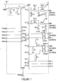
- Fig. 1 is a block diagram illustrating the circuit configuration of the high-frequency module 10 according to the present embodiment.
- a switch element SWIC includes a single common terminal PIC0 and nine individual terminals PIC11 to PIC19.
- the switch element SWIC includes a ground terminal PGND used for connecting to a ground GND.
- the ground terminal PGND connects to a ground port electrode PMGND in the high-frequency module 10, used for an external connection.
- the switch element SWIC includes a driving voltage application terminal PICVdd and a plurality of control voltage application terminals PICVc1, PICVc2, PICVc3, and PICVc4.
- the driving voltage application terminal PICVdd connects to a power supply system port electrode PMVdd in the high-frequency module 10, used for an external connection.
- the control voltage application terminals PICVc1, PICVc2, PICVc3, and PICVc4 connect to power supply system port electrodes PMVc1, PMVc2, PMVc3, and PMVc4 in the high-frequency module 10, respectively, used for external connections.
- the switch element SWIC is driven using a driving voltage Vdd applied from the driving voltage application terminal PICVdd.
- Vdd applied from the driving voltage application terminal PICVdd.
- the switch IC element SWIC connects the single common terminal PIC0 to one of the nine individual terminals PIC11 to PIC19.
- the common terminal PIC0 connects to an antenna connection external terminal PMan in the high-frequency module 10 through an antenna side matching circuit 11 doubling as an ESD circuit.
- the antenna connection external terminal PMan connects to an external antenna ANT.
- the antenna side matching circuit 11 includes an inductor L2 connected in series between the antenna connection external terminal PMan and the common terminal PIC0. An end portion on the antenna connection external terminal PMan side of the inductor L2 is connected to the ground GND through a capacitor C1. An end portion on the common terminal PIC0 side of the inductor L2 is connected to the ground GND through an inductor L1 mainly functioning as an ESD element.
- the first individual terminal PIC11 connects to a first individual external terminal PMtL in the high-frequency module 10 through a transmission side filter 12A.
- the first individual external terminal PMtL is a terminal into which the transmission signal of the GSM850 or the transmission signal of the GSM900 is input from the outside.
- the transmission side filter 12A includes inductors GLt1 and GLt2 connected in series between the first individual terminal PIC11 and the first individual external terminal PMtL. At this time, the inductor GLt1 and the inductor GLt2 are connected in this order from a first individual terminal PIC11 side. An end portion on the first individual terminal PIC11 side of the inductor GLt1 is connected to the ground GND through a capacitor GCu1. A connection point between the inductors GLt1 and GLt2 is connected to the ground GND through a capacitor GCu2. An end portion on the first individual external terminal PMtL side of the inductor GLt2 is connected to the ground GND through a capacitor GCu3.
- a capacitor GCc1 is connected in parallel to the inductor GLt1.
- a capacitor GCc2 is connected in parallel to the inductor GLt2.
- a filter is realized whose pass band corresponds to the operation frequencies of the transmission signal of the GSM850 and the transmission signal of the GSM900 and whose stop band corresponds to a high frequency band including the second harmonic waves and the third harmonic waves of the transmission signal of the GSM850 and the transmission signal of the GSM900.
- the second individual terminal PIC12 connects to a second individual external terminal PMtH in the high-frequency module 10 through a transmission side filter 12B.
- the second individual external terminal PMtH is a terminal into which the transmission signal of the GSM1800 or the transmission signal of the GSM1900 is input from the outside.
- the transmission side filter 12B includes inductors DLt1 and DLt2 connected in series between the second individual terminal PIC12 and the second individual external terminal PMtH. At this time, the inductor DLt1 and the inductor DLt2 are connected in this order from a second individual terminal PIC12 side. A connection point between the inductors DLt1 and DLt2 is connected to the ground GND through a capacitor DCu2. An end portion on the second individual external terminal PMtH side of the inductor DLt2 is connected to the ground GND through a capacitor DCu3.
- a capacitor DCc1 is connected in parallel to the inductor DLt1.
- a filter is realized whose pass band corresponds to the operation frequencies of the transmission signal of the GSM1800 and the transmission signal of the GSM1900 and whose stop band corresponds to a high frequency band including the second harmonic waves and the third harmonic waves of the transmission signal of the GSM1800 and the transmission signal of the GSM1900.
- the third individual terminal PIC13 connects to the unbalanced terminal of a SAW filter SAW1L in a SAW duplexer DUPL.
- the SAW filter SAW1L is a filter whose pass band corresponds to the frequency band of the reception signal of the GSM850, and includes a balanced-to-unbalanced conversion function.
- the balanced terminal of the SAW filter SAW1L connects to a third individual external terminal PMrL1 in the high-frequency module 10.
- the third individual external terminal PMrL1 is a terminal from which the reception signal of the GSM850 is output.
- the fourth individual terminal PIC14 connects to the unbalanced terminal of a SAW filter SAW2L in the SAW duplexer DUPL.
- a matching inductor L3 is connected between a transmission line connecting the fourth individual terminal PIC14 and the SAW filter SAW2L to each other and a ground potential.
- the SAW filter SAW2L is a filter whose pass band corresponds to the frequency band of the reception signal of the GSM900, and includes a balanced-to-unbalanced conversion function.
- the balanced terminal of the SAW filter SAW2L connects to a fourth individual external terminal PMrL2 in the high-frequency module 10.
- the fourth individual external terminal PMrL2 is a terminal from which the reception signal of the GSM900 is output.
- the fifth individual terminal PIC15 connects to the unbalanced terminal of a SAW filter SAW1H in a SAW duplexer DUPH.
- a matching inductor L4 is connected between a transmission line connecting the fifth individual terminal PIC15 and the SAW filter SAW1H to each other and the ground potential.
- the SAW filter SAW1H is a filter whose pass band corresponds to the frequency band of the reception signal of the GSM1800, and includes a balanced-to-unbalanced conversion function.
- the balanced terminal of the SAW filter SAW1H connects to a fifth individual external terminal PMrH1 in the high-frequency module 10.
- the fifth individual external terminal PMrH1 is a terminal from which the reception signal of the GSM1800 is output.
- the sixth individual terminal PIC16 connects to the unbalanced terminal of a SAW filter SAW2H in the SAW duplexer DUPH.
- a matching inductor L5 is connected between a transmission line connecting the sixth individual terminal PIC16 and the SAW filter SAW2H to each other and the ground potential.
- the SAW filter SAW2H is a filter whose pass band corresponds to the frequency band of the reception signal of the GSM1900, and includes a balanced-to-unbalanced conversion function.
- the balanced terminal of the SAW filter SAW2H connects to a sixth individual external terminal PMrH2 in the high-frequency module 10.
- the sixth individual external terminal PMrH2 is a terminal from which the reception signal of the GSM1900 is output.
- the seventh individual terminal PIC17 connects to a seventh individual external terminal PMu1 in the high-frequency module 10.
- the seventh individual external terminal PMu1 is a terminal used for inputting and outputting a first UMTS communication signal.
- the eighth individual terminal PIC18 connects to an eighth individual external terminal PMu2 in the high-frequency module 10.
- the eighth individual external terminal PMu2 is a terminal used for inputting and outputting a second UMTS communication signal.
- the ninth individual terminal PIC19 connects to a ninth individual external terminal PMu3 in the high-frequency module 10.
- the ninth individual external terminal PMu3 is a terminal used for inputting and outputting a third UMTS communication signal.
- a high-frequency module 10 is realized on the basis of the following structure.
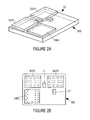
- Figs. 2A and 2B are diagrams for explaining the structure of the high-frequency module 10 according to the present embodiment, Fig. 2A is an external appearance perspective view, and Fig. 2B is an upper surface mounting diagram.
- Fig. 3 is the lamination diagram of the high-frequency module 10.
- the high-frequency module 10 includes a laminated body 900.
- the SAW duplexers DUPL and DUPH and the switch element SWIC are mounted in the upper surface of the laminated body 900.
- mount inductor elements are mounted that realize the inductors L1 and L3.
- the laminated body 900 is obtained by laminating a predetermined number of dielectric layers, and realizes a portion other than the above-mentioned individual mount circuit elements, in the high-frequency module 10, using inner layer electrode patterns.
- inner layer electrode patterns In addition, while, in the present embodiment, a detailed layout pattern is not illustrated, each of the above-mentioned port electrodes used for external connections is formed in a predetermined array in the bottom surface of the laminated body 900.
- the laminated body 900 is obtained by laminating dielectric layers of 14 layers, a predetermined electrode pattern used for configuring the high-frequency module 10 is formed in each dielectric layer, and via electrodes establishing interlayer connections are formed.
- the via electrodes are indicated by circles illustrated in each layer in Fig. 3 .
- an uppermost layer is a first layer PL1
- the numerical value of a layer increases with the layer being located on a lower layer side
- a lowermost layer is a fourteenth layer PL14, the descriptions thereof will be performed.
- element mounting electrodes are formed that are used for mounting the SAW duplexers DUPL and DUPH, the switch element SWIC, and the inductors L1 and L3.
- the ground electrode GND of an inner layer is formed in the substantially whole upper surface of the fifth layer PL5.
- one facing electrode of each of the capacitors GCu1 and GCu3 is formed in the upper surface of the sixth layer PL6, one facing electrode of each of the capacitors GCu1 and GCu3 is formed.
- the other facing electrode of each of these capacitors GCu1 and GCu3 is the ground electrode GND of the fifth layer PL5.
- substantially linear electrode patterns individually configuring the inductors GLt1, GLt2, DLt1, DLt2, L2, L4, and L5 are formed.
- substantially linear electrode patterns individually configuring the inductors GLt1, GLt2, DLt1, DLt2, L2, L4, and L5 are also formed.
- substantially linear electrode patterns individually configuring the inductors GLt1, GLt2, L2, L4, and L5 are formed.
- one facing electrode of each of the capacitors GCu2, DCc1, DCu2, and C1 are formed in the upper surface of the twelfth layer PL12.
- one facing electrode of the capacitor GCu2 also functions as the other facing electrode of each of the capacitors GCc1 and GCc2.
- the ground electrode GND of an inner layer is formed in the substantially whole upper surface of the thirteenth layer PL13.
- the ground electrode GND also functions as the other facing electrode of each of the capacitors GCu2, DCc1, DCu2, and C1.
- electrodes configuring the first individual external terminal PMtL to the ninth individual external terminal PMu3, an electrode configuring the antenna connection external terminal PMan, and an external-connection ground electrode are formed in an array. These electrodes are formed in an array so as to realize the circuit illustrated in Fig. 1 along with the above-mentioned electrode patterns in the individual layers.
- Fig. 4 is the magnification plan view of layers in which individual inductors within the laminated body 900 are formed.
- each of the inductors GLt1 and GLt2 is configured using substantially linear electrode patterns formed in the seventh layer PL7, the eighth layer PL8, the ninth layer PL9, and the tenth layer PL10 and the via electrodes establishing interlayer connections.
- the substantially linear electrode pattern of the inductor GLt2 is formed so as to rotate from an end portion on a side connecting to the first individual external terminal PMtL, in a clockwise fashion. End portions on the side connecting to the first individual external terminal PMtL and on an opposite side are connected to a substantially linear electrode pattern configuring the inductor GLt2 in the eighth layer PL8, through via electrodes penetrating the seventh layer PL7.
- the substantially linear electrode pattern of the inductor GLt2 is formed so as to rotate from an end portion connecting to a via electrode leading from the seventh layer PL7, in a clockwise fashion. End portions on a side connecting to the via electrode penetrating the seventh layer PL7 and on an opposite side are connected to a substantially linear electrode pattern configuring the inductor GLt2 in the ninth layer PL9, through via electrodes penetrating the eighth layer PL8.
- the substantially linear electrode pattern of the inductor GLt2 is formed so as to rotate from an end portion connecting to a via electrode penetrating the eighth layer PL8, in a clockwise fashion. End portions on a side connecting to the via electrode penetrating the eighth layer PL8 and on an opposite side are connected to a substantially linear electrode pattern configuring the inductor GLt2 in the tenth layer PL10, through via electrodes penetrating the ninth layer PL9.
- the substantially linear electrode pattern of the inductor GLt2 is formed so as to rotate from an end portion connecting to a via electrode penetrating the ninth layer PL9, in a clockwise fashion. End portions on a side connecting to the via electrode penetrating the ninth layer PL9 and on an opposite side are connected to a substantially linear electrode pattern configuring the inductor GLt1.
- the inductor GLt2 has a shape winding in a clockwise fashion so as to be headed from the seventh layer PL7 to the tenth layer PL10.
- the substantially linear electrode pattern of the inductor GLt1 is formed so as to rotate from an end portion connecting to the inductor GLt2, in a clockwise fashion. End portions on a side connecting to the inductor GLt2 and on an opposite side are connected to a substantially linear electrode pattern configuring the inductor GLt1 in the ninth layer PL9, through via electrodes penetrating the ninth layer PL9.
- the substantially linear electrode pattern of the inductor GLt1 is formed so as to rotate from an end portion connecting to a via electrode penetrating the ninth layer PL9, in a clockwise fashion. End portions on a side connecting to the via electrode penetrating the ninth layer PL9 and on an opposite side are connected to a substantially linear electrode pattern configuring the inductor GLt1 in the eighth layer PL8, through via electrodes penetrating the eighth layer PL8.
- the substantially linear electrode pattern of the inductor GLt1 is formed so as to rotate from an end portion connecting to a via electrode penetrating the eighth layer PL8, in a clockwise fashion. End portions on a side connecting to the via electrode penetrating the eighth layer PL8 and on an opposite side are connected to a substantially linear electrode pattern configuring the inductor GLt1 in the seventh layer PL7, through via electrodes penetrating the seventh layer PL7.
- the substantially linear electrode pattern of the inductor GLt1 is formed so as to rotate from an end portion connecting to a via electrode penetrating the seventh layer PL7, in a clockwise fashion. End portions on a side connecting to the via electrode penetrating the seventh layer PL7 and on an opposite side are connected to the first individual terminal PIC11.
- the inductor GLt1 has a shape winding in a clockwise fashion so as to be headed from the tenth layer PL10 to the seventh layer PL7.
- the inductors DLt1 and DLt2 are configured using substantially linear electrode patterns formed in the seventh layer PL7, the eighth layer PL8, and the ninth layer PL9 and the via electrodes establishing interlayer connections.
- the substantially linear electrode pattern of the inductor DLt2 is formed so as to rotate from an end portion on a side connecting to the second individual external terminal PMtH, in a clockwise fashion. End portions on the side connecting to the second individual external terminal PMtH and on an opposite side are connected to a substantially linear electrode pattern configuring the inductor DLt2 in the eighth layer PL8, through via electrodes penetrating the seventh layer PL7.
- the substantially linear electrode pattern of the inductor DLt2 is formed so as to rotate from an end portion connecting to a via electrode penetrating the seventh layer PL7, in a clockwise fashion. End portions on a side connecting to the via electrode penetrating the seventh layer PL7 and on an opposite side are connected to a substantially linear electrode pattern configuring the inductor DLt2 in the ninth layer PL9, through via electrodes penetrating the eighth layer PL8.
- the substantially linear electrode pattern of the inductor DLt2 is formed so as to rotate from an end portion connecting to a via electrode penetrating the eighth layer PL8, in a clockwise fashion. End portions on a side connecting to the via electrode penetrating the eighth layer PL8 and on an opposite side are connected to a substantially linear electrode pattern configuring the inductor DLt1.
- the inductor DLt2 has a shape winding in a clockwise fashion so as to be headed from the seventh layer PL7 to the ninth layer PL9.
- the substantially linear electrode pattern of the inductor DLt1 is formed so as to rotate from an end portion connecting to the inductor DLt2, in a clockwise fashion. End portions on a side connecting to the inductor DLt2 and on an opposite side are connected to an electrode pattern configuring the inductor DLt1 in the eighth layer PL8, through via electrodes penetrating the eighth layer PL8.
- the substantially linear electrode pattern of the inductor DLt1 is formed so as to rotate from an end portion connecting to a via electrode penetrating the eighth layer PL8, in a clockwise fashion. End portions on a side connecting to the via electrode leading from the eighth layer PL8 and on an opposite side are connected to an electrode pattern configuring the inductor DLt1 in the seventh layer PL7, through via electrodes penetrating the seventh layer PL7.
- the substantially linear electrode pattern of the inductor DLt1 is formed so as to rotate from an end portion connecting to a via electrode penetrating the seventh layer PL7, in a clockwise fashion. End portions on a side connecting to the via electrode penetrating the seventh layer PL7 and on an opposite side are connected to the second individual terminal PIC12.
- the inductor DLt1 has a shape winding in a clockwise fashion so as to be headed from the ninth layer PL9 to the seventh layer PL7.
- the inductors L2, L4, and L5 are configured using substantially linear electrode patterns formed in the seventh layer PL7, the eighth layer PL8, the ninth layer PL9, and the tenth layer PL10 and the via electrodes establishing interlayer connections.
- the substantially linear electrode pattern of the inductor L2 is formed so as to rotate from an end portion on a side connecting to the common terminal PIC0, in a clockwise fashion. End portions on the side connecting to the common terminal PIC0 and on an opposite side are connected to an electrode pattern configuring the inductor L2 in the eighth layer PL8, through via electrodes penetrating electrodes in the seventh layer PL7.
- the substantially linear electrode pattern of the inductor L2 is formed so as to rotate from an end portion connecting to a via electrode penetrating the seventh layer PL7, in a clockwise fashion. End portions on a side connecting to the via electrode penetrating the seventh layer PL7 and on an opposite side are connected to an electrode pattern configuring the inductor L2 in the ninth layer PL9, through via electrodes penetrating the eighth layer PL8.
- the substantially linear electrode pattern of the inductor L2 is formed so as to rotate from an end portion connecting to a via electrode penetrating the eighth layer PL8, in a clockwise fashion. End portions on a side connecting to the via electrode penetrating the eighth layer PL8 and on an opposite side are connected to an electrode pattern configuring the inductor L2 in the tenth layer PL10, through via electrodes penetrating the ninth layer PL9.
- the substantially linear electrode pattern of the inductor L2 is formed so as to rotate from an end portion connecting to a via electrode penetrating the ninth layer PL9, in a clockwise fashion. End portions on a side connecting to the via electrode penetrating the ninth layer PL9 and on an opposite side are connected to the antenna connection external terminal PMan.
- the inductor L2 has a shape winding in a clockwise fashion so as to be headed from the seventh layer PL7 to the tenth layer PL10.
- the inductors GLt1 and GLt2 inserted in series in the transmission line configuring the transmission side filter 12A, the inductors DLt1 and DLt2 inserted in series in the transmission line configuring the transmission side filter 12B, and the inductor L2 inserted in series in the transmission line configuring the antenna side matching circuit 11 are formed within the laminated body 900 so that the directions of the generated magnetic fields coincide with one another. Accordingly, the magnetic fields generated by the inductors GLt1, GLt2, DLt1, DLt2, and L2 turn out to be independent of one another, and may avoid being electromagnetic-field-coupled to one another.
- each of the inductors GLt1, GLt2, DLt1, DLt2, and L2 may be possible to cause each of the inductors GLt1, GLt2, DLt1, DLt2, and L2 to function with having a characteristic complying with circuit design. Accordingly, it may be possible to sufficiently obtain the attenuation characteristics of the second harmonic waves and the attenuations of the third harmonic waves of the transmission side filters 12A and 12B.
- the inductors GLt1, GLt2, DLt1, DLt2, L2, L4, and L5 are formed on the same layers in three layers including the seventh layer, the eighth layer, and the ninth layer.
- the inductors GLt1, GLt2, DLt1, DLt2, L4, and L5 are formed so as not to overlap with one another when the laminated body 900 is viewed along the lamination direction.
- inner layer ground electrodes GND are formed in dielectric layers PL5 and PL13 so as to sandwich therebetween dielectric layers PL7, PL8, PL9, and PL10 in which the individual inductors GLt1, GLt2, DLt1, DLt2, L2, L4, and L5 are formed.
- the ground electrodes GND are formed so as to contain the forming regions of the inductors GLt1, GLt2, DLt1, DLt2, L2, L4, and L5.
- the laminated body 900 is formed so that, by adjusting the thicknesses of the dielectric layers, distances between the substantially linear electrode patterns of the inductors GLt1, GLt2, DLt1, DLt2, L2, L4, and L5 in the dielectric layer PL7 and the ground electrode GND in the dielectric layer PL5 and distances between the substantially linear electrode patterns of the inductors GLt1, GLt2, L2, L4, and L5 in the dielectric layer PL10 and the ground electrode GND in the dielectric layer PL13 are shorter than distances between the inductors GLt1, GLt2, DLt1, DLt2, L2, L4, and L5 on a plane surface on the same layer.
- each of the inductors GLt1, GLt2, DLt1, DLt2, L2, L4, and L5 is electromagnetic-field-coupled to the ground electrode GND along the lamination direction, and magnetic fields individually generated in the inductors turn out to be independent of one another. Accordingly, it may be possible to avoid the individual inductors from being electromagnetic-field-coupled to one another on a plane surface within a layer. Accordingly, each inductor functions with having an element value complying with circuit design, it may be possible to suppress the characteristic degradation of each of the transmission side filters 12A and 12B, the leaks of the second harmonic wave and the third harmonic wave between the transmission side circuit and a circuit on the antenna side, and leaking of the reception signal to the transmission side circuit.
- distances on a plane surface between the substantially linear electrode pattern of the inductor L2 in the antenna side matching circuit 11 and the substantially linear electrode patterns of the inductors GLt1, GLt2, DLt1, and DLt2 in the transmission side circuit are made longer than distances on a plane surface between the substantially linear electrode patterns of the inductors GLt1, GLt2, DLt1, and DLt2 in the transmission side circuit.
- the inductor L2 when the inductor L2 is formed with the common terminal PIC0 of the switch element SWIC as a starting point so as to wind in a substantially spiral shape clockwise from the upper surface side of the laminated body 900 to the bottom surface side thereof, the inductors GLt1, GLt2, DLt1, and DLt2 are formed with the first individual external terminal PMtL and the second individual external terminal PMtH as starting points so as to wind in a substantially spiral shape clockwise from the upper surface side of the laminated body 900 to the bottom surface side thereof, the first individual external terminal PMtL and the second individual external terminal PMtH serving as the input ends of the transmission signals.
- the inductor L2 when the inductor L2 is formed in the same substantially spiral shape in a counterclockwise fashion, all of the inductors GLt1, GLt2, DLt1, and DLt2 may be formed so as to wind in a substantially spiral shape counterclockwise from the upper surface side of the laminated body 900 to the bottom surface side thereof.
- the circling direction of a substantially linear electrode pattern configuring each inductor may be determined so that the direction of a magnetic field generated in the inductor L2 connected in series to the signal transmission path on the antenna side and the directions of magnetic fields generated in the inductors GLt1, GLt2, DLt1, and DLt2 connected in series to the signal transmission paths within the transmission side circuit coincide with one another.
Landscapes
- Engineering & Computer Science (AREA)
- Computer Networks & Wireless Communication (AREA)
- Signal Processing (AREA)
- Transceivers (AREA)
- Filters And Equalizers (AREA)
- Coils Or Transformers For Communication (AREA)
Abstract
Description
- The present invention relates to a high-frequency module transmitting and receiving a plurality of communication signals using a common antenna.
- In the past, various kinds of high-frequency modules have been designed that transmit and receive a plurality of communication signals using a common antenna, each of the plural communication signals utilizing a different frequency band. For example, as such a high-frequency module, a high-frequency module may be cited that is described in Japanese Unexamined Patent Application Publication No.
2008-10995 - The high-frequency module described in Japanese Unexamined Patent. Application Publication No.
2008-10995 - In the case of such a high-frequency module utilizing the laminated body, a circuit configuration other than mounted components such as the switch element and the SAW filter is realized using inner layer electrode patterns formed within the laminated body.
- However, when the high-frequency module is downsized, electromagnetic field coupling occurs between circuit elements realized by these inner layer electrode patterns. For example, a plurality of inductors on a transmission path transmitting one communication signal are electromagnetic-field-coupled to one another, an inductor of a circuit on the common terminal side of the switch element is electromagnetic-field-coupled to an inductor of a circuit on the individual terminal side of the switch element, or inductors individually connected onto a plurality of different transmission paths are electromagnetic-field-coupled to one another. In such a case, it may be hard to obtain a desired transmission characteristic. For example, an inductor of a low pass filter used for a second harmonic wave and an inductor of a low pass filter used for a third harmonic wave, connected in series onto one transmission circuit, are electromagnetic-field-coupled to each other, and hence it may be hard to fully attenuate the second harmonic wave and the third harmonic wave of a communication signal transmitted through the corresponding transmission circuit. In addition, an inductor used for an antenna side matching circuit is electromagnetic-field-coupled to an inductor of a low pass filter used for a second harmonic wave or an inductor of a low pass filter used for a third harmonic wave, connected in series onto a transmission circuit, and hence it may be hard to fully attenuate the harmonic wave of a communication signal transmitted through the corresponding transmission circuit.
- Accordingly, it is an object of the present invention to realize a high-frequency module capable of suppressing electromagnetic field coupling between inductors formed in a laminated body and obtaining a desired characteristic while being downsized.
- According to preferred embodiments of the present invention, there is provided a high-frequency module including a laminated body configured to include an antenna connection external terminal connecting to an antenna and a plurality of individual external terminals to each of which a transmission circuit used for transmitting a plurality of communication signals and a reception circuit used for receiving the plural communication signals are connected; and a switch element configured to be mounted in the laminated body and include a common terminal connecting to the antenna connection external terminal and a plurality of individual terminals connecting to the plural individual external terminals. The high-frequency module includes a plurality of inductors on an individual terminal side, which are formed within the laminated body and individually connected in series between the plural individual terminals and the plural individual external terminals. These plural inductors on the individual terminal side do not overlap with one another in a state in which the laminated body is viewed along a lamination direction, and are formed within the laminated body so that directions of generated magnetic fields coincide with one another.
- According to this configuration, it may be possible to sufficiently suppress magnetic field coupling between the inductors on the individual terminal side. Accordingly, each inductor functions so as to comply with circuit design, and a desired transmission characteristic is realized.
- In addition, it is desirable that the high-frequency module according to preferred embodiments of the present invention includes the following configuration. The high-frequency module includes an inductor on an antenna side, configured to be connected in series between the antenna connection external terminal and the common terminal. The inductor on the antenna side and the plural inductors on the individual terminal side do not overlap with one another in a state in which the laminated body is viewed along the lamination direction, and are formed within the laminated body so that directions of generated magnetic fields coincide with one another.
- According to this configuration, it may be possible to sufficiently suppress magnetic field coupling between the inductor on the antenna side and the inductor on the individual terminal side. Accordingly, each of the inductors on both the antenna side and the individual terminal side of the switch element functions so as to comply with circuit design, and a desired transmission characteristic is realized.
- In addition, it is desirable that the high-frequency module according to preferred embodiments of the present invention includes the following configuration. In the high-frequency module, inner layer electrode patterns of the plural inductors on the individual terminal side are formed in a plurality of same layers of the laminated body.
- According to this configuration, each inductor is formed in the same layer in the laminated body, and hence it may be possible to suppress magnetic field coupling along the lamination direction. Accordingly, it may be possible to more desirably suppress coupling between inductors.
- In addition, it is desirable that the high-frequency module according to preferred embodiments of the present invention includes the following configuration. In the high-frequency module, an inner layer electrode pattern of the inductor on the antenna side and the inner layer electrode patterns of the plural inductors on the individual terminal side are formed in the plural same layers of the laminated body. Distances between the inner layer electrode pattern of the inductor on the antenna side and the inner layer electrode patterns of the plural inductors on the individual terminal side in a state of being viewed in the lamination direction are longer than distances between the inner layer electrode patterns of the plural inductors on the individual terminal side.
- According to this configuration, it may be possible to more desirably suppress magnetic field coupling between the inductor on the antenna side and the inductors on the individual terminal side. Accordingly, it may be possible to avoid an undesirable signal from leaking from a predetermined circuit on the individual terminal side to the antenna. Accordingly, it may be possible to avoid the second harmonic wave or the third harmonic wave of a transmission signal from leaking from the transmission circuit to the antenna side. In addition, it may be possible to avoid a communication signal from the antenna from going round and cutting in an unintended circuit on the individual terminal side without passing through the switch element. Accordingly, it may be possible to transmit a reception signal from the antenna to a desired reception circuit with low loss.
- In addition, it is desirable that the high-frequency module according to preferred embodiments of the present invention includes the following configuration. In the high-frequency module, an inner layer ground electrode configured to be formed in an upper layer and a lower layer of a layer in which the inner layer electrode pattern of the inductor in the laminated body is formed, so as to contain a forming region of the inner layer electrode pattern of the inductor when being viewed from the lamination direction. A distance between the inner layer electrode pattern of the inductor closest to the inner layer ground electrode and the inner layer ground electrode is shorter than distances between the inner layer electrode patterns individually forming the plural inductors.
- According to this configuration, each inductor is sandwiched in the lamination direction by the inner layer ground electrode, and each inductor and the inner layer ground electrode are adjacent to each other. Therefore, it may be possible to more desirably realize the independence of a magnetic field generated in each inductor, namely, the suppression of coupling between magnetic fields generated in the individual inductors.
- In addition, it is desirable that the high-frequency module according to preferred embodiments of the present invention includes the following configuration. In the high-frequency module, the plural inductors on the individual terminal side are inductors of a filter circuit connected to the transmission circuit.
- According to this configuration, an example is illustrated in which, as the above-mentioned inductors on the individual terminal side, the inductors of the filter circuit connecting to the transmission circuit are used. Since the transmission circuit transmits a high-power transmission signal, while it may be easy for inductors to be magnetic-field-coupled to one another, magnetic field coupling between the inductors is suppressed by utilizing the above-mentioned configuration. Accordingly, it may be possible to cause the transmission circuit to have desired filter characteristics (a transmission characteristic and an attenuation characteristic).
- In addition, it is desirable that the high-frequency module according to preferred embodiments of the present invention includes the following configuration. In the high-frequency module, the filter circuit is a low pass filter attenuating a second harmonic wave and a third harmonic wave of a transmitted communication signal. The plural inductors on the individual terminal side include a series inductor used for attenuating the second harmonic wave and a series inductor used for attenuating the third harmonic wave.
- In this configuration, a more specific example of a circuit configuration is illustrated when being applied to the above-mentioned transmission circuit. By adopting such a configuration, it may be possible to obtain the attenuations of the second harmonic wave and the third harmonic wave of the transmission signal, which are sufficient attenuations complying with circuit design.
- According to preferred embodiments of the present invention, a high-frequency module may be realized that obtains a desired characteristic while being downsized.
- Other features, elements, characteristics and advantages of the present invention will become more apparent from the following detailed description of preferred embodiments of the present invention with reference to the attached drawings.
-
-
Fig. 1 is a block diagram illustrating a circuit configuration of a high-frequency module according to an embodiment of the present invention; -
Fig. 2A is an external appearance perspective view of the high-frequency module, andFig. 2B is a mounting state diagram of individual circuit elements; -
Fig. 3 is a lamination diagram of the high-frequency module; and -
Fig. 4 is a magnification plan view of layers in which individual inductors within a laminated body are formed. - A high-frequency module according to a first embodiment of the present invention will be described with reference to drawings. In the present embodiment, a high-frequency module will be described that transmits and receives a communication signal of a global system for mobile communications (GSM) 850, a communication signal of a GSM900, a communication signal of a GSM1800, and a communication signal of a GSM1900 and transmits and receives a universal mobile telecommunications system (UMTS) communication signal such as a wideband code division multiple access (W-CDMA) communication system or the like. In addition, while, in the present embodiment, a case is illustrated in which a transmission and reception circuit for three types of UMTS communication signals is provided, the transmission and reception circuit for these UMTS communication signals may also be omitted.
- First, the circuit configuration of a high-
frequency module 10 of the present embodiment will be described.Fig. 1 is a block diagram illustrating the circuit configuration of the high-frequency module 10 according to the present embodiment. - A switch element SWIC includes a single common terminal PIC0 and nine individual terminals PIC11 to PIC19. The switch element SWIC includes a ground terminal PGND used for connecting to a ground GND. The ground terminal PGND connects to a ground port electrode PMGND in the high-
frequency module 10, used for an external connection. - The switch element SWIC includes a driving voltage application terminal PICVdd and a plurality of control voltage application terminals PICVc1, PICVc2, PICVc3, and PICVc4. The driving voltage application terminal PICVdd connects to a power supply system port electrode PMVdd in the high-
frequency module 10, used for an external connection. The control voltage application terminals PICVc1, PICVc2, PICVc3, and PICVc4 connect to power supply system port electrodes PMVc1, PMVc2, PMVc3, and PMVc4 in the high-frequency module 10, respectively, used for external connections. - The switch element SWIC is driven using a driving voltage Vdd applied from the driving voltage application terminal PICVdd. On the basis of the combination of control voltages Vc1, Vc2, Vc3, and VC4 applied to the plural control voltage application terminals PICVc1, PICVc2, PICVc3, and PICVc4, respectively, the switch IC element SWIC connects the single common terminal PIC0 to one of the nine individual terminals PIC11 to PIC19.
- The common terminal PIC0 connects to an antenna connection external terminal PMan in the high-
frequency module 10 through an antennaside matching circuit 11 doubling as an ESD circuit. The antenna connection external terminal PMan connects to an external antenna ANT. - The antenna
side matching circuit 11 includes an inductor L2 connected in series between the antenna connection external terminal PMan and the common terminal PIC0. An end portion on the antenna connection external terminal PMan side of the inductor L2 is connected to the ground GND through a capacitor C1. An end portion on the common terminal PIC0 side of the inductor L2 is connected to the ground GND through an inductor L1 mainly functioning as an ESD element. - The first individual terminal PIC11 connects to a first individual external terminal PMtL in the high-
frequency module 10 through atransmission side filter 12A. The first individual external terminal PMtL is a terminal into which the transmission signal of the GSM850 or the transmission signal of the GSM900 is input from the outside. - The
transmission side filter 12A includes inductors GLt1 and GLt2 connected in series between the first individual terminal PIC11 and the first individual external terminal PMtL. At this time, the inductor GLt1 and the inductor GLt2 are connected in this order from a first individual terminal PIC11 side. An end portion on the first individual terminal PIC11 side of the inductor GLt1 is connected to the ground GND through a capacitor GCu1. A connection point between the inductors GLt1 and GLt2 is connected to the ground GND through a capacitor GCu2. An end portion on the first individual external terminal PMtL side of the inductor GLt2 is connected to the ground GND through a capacitor GCu3. - A capacitor GCc1 is connected in parallel to the inductor GLt1. By setting the element value of this parallel resonance circuit to a predetermined value, a characteristic is realized that desirably attenuates the frequencies of the second harmonic waves of transmission signals input from the first individual external terminal PMtL, namely, the GSM850 transmission signal and the GSM900 transmission signal.
- A capacitor GCc2 is connected in parallel to the inductor GLt2. By setting the element value of this parallel resonance circuit to a predetermined value, a characteristic is realized that desirably attenuates the frequencies of the third harmonic waves of the transmission signals input from the first individual external terminal PMtL, namely, the GSM850 transmission signal and the GSM900 transmission signal.
- Furthermore, by setting the element value of each of the inductors and the capacitors configuring the
transmission side filter 12A, a filter is realized whose pass band corresponds to the operation frequencies of the transmission signal of the GSM850 and the transmission signal of the GSM900 and whose stop band corresponds to a high frequency band including the second harmonic waves and the third harmonic waves of the transmission signal of the GSM850 and the transmission signal of the GSM900. - The second individual terminal PIC12 connects to a second individual external terminal PMtH in the high-
frequency module 10 through atransmission side filter 12B. The second individual external terminal PMtH is a terminal into which the transmission signal of the GSM1800 or the transmission signal of the GSM1900 is input from the outside. - The
transmission side filter 12B includes inductors DLt1 and DLt2 connected in series between the second individual terminal PIC12 and the second individual external terminal PMtH. At this time, the inductor DLt1 and the inductor DLt2 are connected in this order from a second individual terminal PIC12 side. A connection point between the inductors DLt1 and DLt2 is connected to the ground GND through a capacitor DCu2. An end portion on the second individual external terminal PMtH side of the inductor DLt2 is connected to the ground GND through a capacitor DCu3. - A capacitor DCc1 is connected in parallel to the inductor DLt1. By setting the element value of this parallel resonance circuit to a predetermined value, a characteristic is realized that desirably attenuates the frequencies of the second harmonic waves of transmission signals input from the second individual external terminal PMtH, namely, the GSM1800 transmission signal and the GSM1900 transmission signal.
- Furthermore, by setting the element value of each of the inductors and the capacitors configuring the
transmission side filter 12B, a filter is realized whose pass band corresponds to the operation frequencies of the transmission signal of the GSM1800 and the transmission signal of the GSM1900 and whose stop band corresponds to a high frequency band including the second harmonic waves and the third harmonic waves of the transmission signal of the GSM1800 and the transmission signal of the GSM1900. - The third individual terminal PIC13 connects to the unbalanced terminal of a SAW filter SAW1L in a SAW duplexer DUPL. The SAW filter SAW1L is a filter whose pass band corresponds to the frequency band of the reception signal of the GSM850, and includes a balanced-to-unbalanced conversion function. The balanced terminal of the SAW filter SAW1L connects to a third individual external terminal PMrL1 in the high-
frequency module 10. The third individual external terminal PMrL1 is a terminal from which the reception signal of the GSM850 is output. - The fourth individual terminal PIC14 connects to the unbalanced terminal of a SAW filter SAW2L in the SAW duplexer DUPL. A matching inductor L3 is connected between a transmission line connecting the fourth individual terminal PIC14 and the SAW filter SAW2L to each other and a ground potential. The SAW filter SAW2L is a filter whose pass band corresponds to the frequency band of the reception signal of the GSM900, and includes a balanced-to-unbalanced conversion function. The balanced terminal of the SAW filter SAW2L connects to a fourth individual external terminal PMrL2 in the high-
frequency module 10. The fourth individual external terminal PMrL2 is a terminal from which the reception signal of the GSM900 is output. - The fifth individual terminal PIC15 connects to the unbalanced terminal of a SAW filter SAW1H in a SAW duplexer DUPH. A matching inductor L4 is connected between a transmission line connecting the fifth individual terminal PIC15 and the SAW filter SAW1H to each other and the ground potential. The SAW filter SAW1H is a filter whose pass band corresponds to the frequency band of the reception signal of the GSM1800, and includes a balanced-to-unbalanced conversion function. The balanced terminal of the SAW filter SAW1H connects to a fifth individual external terminal PMrH1 in the high-
frequency module 10. The fifth individual external terminal PMrH1 is a terminal from which the reception signal of the GSM1800 is output. - The sixth individual terminal PIC16 connects to the unbalanced terminal of a SAW filter SAW2H in the SAW duplexer DUPH. A matching inductor L5 is connected between a transmission line connecting the sixth individual terminal PIC16 and the SAW filter SAW2H to each other and the ground potential. The SAW filter SAW2H is a filter whose pass band corresponds to the frequency band of the reception signal of the GSM1900, and includes a balanced-to-unbalanced conversion function. The balanced terminal of the SAW filter SAW2H connects to a sixth individual external terminal PMrH2 in the high-
frequency module 10. The sixth individual external terminal PMrH2 is a terminal from which the reception signal of the GSM1900 is output. - The seventh individual terminal PIC17 connects to a seventh individual external terminal PMu1 in the high-
frequency module 10. The seventh individual external terminal PMu1 is a terminal used for inputting and outputting a first UMTS communication signal. The eighth individual terminal PIC18 connects to an eighth individual external terminal PMu2 in the high-frequency module 10. The eighth individual external terminal PMu2 is a terminal used for inputting and outputting a second UMTS communication signal. The ninth individual terminal PIC19 connects to a ninth individual external terminal PMu3 in the high-frequency module 10. The ninth individual external terminal PMu3 is a terminal used for inputting and outputting a third UMTS communication signal. - Such a high-
frequency module 10 is realized on the basis of the following structure.Figs. 2A and 2B are diagrams for explaining the structure of the high-frequency module 10 according to the present embodiment,Fig. 2A is an external appearance perspective view, andFig. 2B is an upper surface mounting diagram.Fig. 3 is the lamination diagram of the high-frequency module 10. - The high-
frequency module 10 includes alaminated body 900. The SAW duplexers DUPL and DUPH and the switch element SWIC are mounted in the upper surface of thelaminated body 900. In addition, in the upper surface of thelaminated body 900, mount inductor elements are mounted that realize the inductors L1 and L3. - The
laminated body 900 is obtained by laminating a predetermined number of dielectric layers, and realizes a portion other than the above-mentioned individual mount circuit elements, in the high-frequency module 10, using inner layer electrode patterns. In addition, while, in the present embodiment, a detailed layout pattern is not illustrated, each of the above-mentioned port electrodes used for external connections is formed in a predetermined array in the bottom surface of thelaminated body 900. - As illustrated in
Fig. 3 , thelaminated body 900 is obtained by laminating dielectric layers of 14 layers, a predetermined electrode pattern used for configuring the high-frequency module 10 is formed in each dielectric layer, and via electrodes establishing interlayer connections are formed. The via electrodes are indicated by circles illustrated in each layer inFig. 3 . In addition, hereinafter, while it is assumed that an uppermost layer is a first layer PL1, the numerical value of a layer increases with the layer being located on a lower layer side, and a lowermost layer is a fourteenth layer PL14, the descriptions thereof will be performed. - In the upper surface of the first layer PL1 serving as the uppermost layer, namely, the upper surface of the
laminated body 900, element mounting electrodes are formed that are used for mounting the SAW duplexers DUPL and DUPH, the switch element SWIC, and the inductors L1 and L3. - In the upper surfaces of the second layer PL2, the third layer PL3, and the fourth layer PL4, lead pattern electrodes are formed. The ground electrode GND of an inner layer is formed in the substantially whole upper surface of the fifth layer PL5.
- In the upper surface of the sixth layer PL6, one facing electrode of each of the capacitors GCu1 and GCu3 is formed. The other facing electrode of each of these capacitors GCu1 and GCu3 is the ground electrode GND of the fifth layer PL5.
- In the upper surface of the seventh layer PL7, substantially linear electrode patterns individually configuring the inductors GLt1, GLt2, DLt1, DLt2, L2, L4, and L5 are formed.
- In the upper surfaces of the eighth layer PL8 and the ninth layer PL9, substantially linear electrode patterns individually configuring the inductors GLt1, GLt2, DLt1, DLt2, L2, L4, and L5 are also formed.
- In the upper surface of the tenth layer PL10, substantially linear electrode patterns individually configuring the inductors GLt1, GLt2, L2, L4, and L5 are formed.
- In the upper surface of the eleventh layer PL11, one facing electrode of each of the capacitors GCc1, GCc2, and DCc1 is formed.
- In the upper surface of the twelfth layer PL12, one facing electrode of each of the capacitors GCu2, DCc1, DCu2, and C1 are formed. In addition, one facing electrode of the capacitor GCu2 also functions as the other facing electrode of each of the capacitors GCc1 and GCc2.
- The ground electrode GND of an inner layer is formed in the substantially whole upper surface of the thirteenth layer PL13. The ground electrode GND also functions as the other facing electrode of each of the capacitors GCu2, DCc1, DCu2, and C1.
- In the bottom surface of the fourteenth layer serving as the lowermost layer, namely, the bottom surface of the
laminated body 900, electrodes configuring the first individual external terminal PMtL to the ninth individual external terminal PMu3, an electrode configuring the antenna connection external terminal PMan, and an external-connection ground electrode are formed in an array. These electrodes are formed in an array so as to realize the circuit illustrated inFig. 1 along with the above-mentioned electrode patterns in the individual layers. - In such a configuration, the individual inductors GLt1, GLt2, DLt1, DLt2, L2, L4, and L5 due to the inner layer electrode patterns are realized on the basis of such a specific configuration as illustrated below.
Fig. 4 is the magnification plan view of layers in which individual inductors within thelaminated body 900 are formed. - As illustrated in
Fig. 4 , each of the inductors GLt1 and GLt2 is configured using substantially linear electrode patterns formed in the seventh layer PL7, the eighth layer PL8, the ninth layer PL9, and the tenth layer PL10 and the via electrodes establishing interlayer connections. - When being viewed from the upper surface, in the seventh layer PL7, the substantially linear electrode pattern of the inductor GLt2 is formed so as to rotate from an end portion on a side connecting to the first individual external terminal PMtL, in a clockwise fashion. End portions on the side connecting to the first individual external terminal PMtL and on an opposite side are connected to a substantially linear electrode pattern configuring the inductor GLt2 in the eighth layer PL8, through via electrodes penetrating the seventh layer PL7.
- When being viewed from the upper surface, in the eighth layer PL8, the substantially linear electrode pattern of the inductor GLt2 is formed so as to rotate from an end portion connecting to a via electrode leading from the seventh layer PL7, in a clockwise fashion. End portions on a side connecting to the via electrode penetrating the seventh layer PL7 and on an opposite side are connected to a substantially linear electrode pattern configuring the inductor GLt2 in the ninth layer PL9, through via electrodes penetrating the eighth layer PL8.
- When being viewed from the upper surface, in the ninth layer PL9, the substantially linear electrode pattern of the inductor GLt2 is formed so as to rotate from an end portion connecting to a via electrode penetrating the eighth layer PL8, in a clockwise fashion. End portions on a side connecting to the via electrode penetrating the eighth layer PL8 and on an opposite side are connected to a substantially linear electrode pattern configuring the inductor GLt2 in the tenth layer PL10, through via electrodes penetrating the ninth layer PL9.
- When being viewed from the upper surface, in the tenth layer PL10, the substantially linear electrode pattern of the inductor GLt2 is formed so as to rotate from an end portion connecting to a via electrode penetrating the ninth layer PL9, in a clockwise fashion. End portions on a side connecting to the via electrode penetrating the ninth layer PL9 and on an opposite side are connected to a substantially linear electrode pattern configuring the inductor GLt1.
- In this way, when being viewed from the upper surface of the
laminated body 900, the inductor GLt2 has a shape winding in a clockwise fashion so as to be headed from the seventh layer PL7 to the tenth layer PL10. - When being viewed from the upper surface, in the tenth layer PL10, the substantially linear electrode pattern of the inductor GLt1 is formed so as to rotate from an end portion connecting to the inductor GLt2, in a clockwise fashion. End portions on a side connecting to the inductor GLt2 and on an opposite side are connected to a substantially linear electrode pattern configuring the inductor GLt1 in the ninth layer PL9, through via electrodes penetrating the ninth layer PL9.
- When being viewed from the upper surface, in the ninth layer PL9, the substantially linear electrode pattern of the inductor GLt1 is formed so as to rotate from an end portion connecting to a via electrode penetrating the ninth layer PL9, in a clockwise fashion. End portions on a side connecting to the via electrode penetrating the ninth layer PL9 and on an opposite side are connected to a substantially linear electrode pattern configuring the inductor GLt1 in the eighth layer PL8, through via electrodes penetrating the eighth layer PL8.
- When being viewed from the upper surface, in the eighth layer PL8, the substantially linear electrode pattern of the inductor GLt1 is formed so as to rotate from an end portion connecting to a via electrode penetrating the eighth layer PL8, in a clockwise fashion. End portions on a side connecting to the via electrode penetrating the eighth layer PL8 and on an opposite side are connected to a substantially linear electrode pattern configuring the inductor GLt1 in the seventh layer PL7, through via electrodes penetrating the seventh layer PL7.
- When being viewed from the upper surface, in the seventh layer PL7, the substantially linear electrode pattern of the inductor GLt1 is formed so as to rotate from an end portion connecting to a via electrode penetrating the seventh layer PL7, in a clockwise fashion. End portions on a side connecting to the via electrode penetrating the seventh layer PL7 and on an opposite side are connected to the first individual terminal PIC11.
- In this way, when the
laminated body 900 is viewed from the upper surface, the inductor GLt1 has a shape winding in a clockwise fashion so as to be headed from the tenth layer PL10 to the seventh layer PL7. - Accordingly, as illustrated in
Fig. 4 , when a signal is transmitted to be headed from the first individual external terminal PMtL to the first individual terminal PIC11, a magnetic field whose axis corresponds to a direction headed from the seventh layer PL7 to the tenth layer PL10 occurs in each of the inductors GLt1 and GLt2. - In addition, the inductors DLt1 and DLt2 are configured using substantially linear electrode patterns formed in the seventh layer PL7, the eighth layer PL8, and the ninth layer PL9 and the via electrodes establishing interlayer connections.
- When being viewed from the upper surface, in the seventh layer PL7, the substantially linear electrode pattern of the inductor DLt2 is formed so as to rotate from an end portion on a side connecting to the second individual external terminal PMtH, in a clockwise fashion. End portions on the side connecting to the second individual external terminal PMtH and on an opposite side are connected to a substantially linear electrode pattern configuring the inductor DLt2 in the eighth layer PL8, through via electrodes penetrating the seventh layer PL7.
- When being viewed from the upper surface, in the eighth layer PL8, the substantially linear electrode pattern of the inductor DLt2 is formed so as to rotate from an end portion connecting to a via electrode penetrating the seventh layer PL7, in a clockwise fashion. End portions on a side connecting to the via electrode penetrating the seventh layer PL7 and on an opposite side are connected to a substantially linear electrode pattern configuring the inductor DLt2 in the ninth layer PL9, through via electrodes penetrating the eighth layer PL8.
- When being viewed from the upper surface, in the ninth layer PL9, the substantially linear electrode pattern of the inductor DLt2 is formed so as to rotate from an end portion connecting to a via electrode penetrating the eighth layer PL8, in a clockwise fashion. End portions on a side connecting to the via electrode penetrating the eighth layer PL8 and on an opposite side are connected to a substantially linear electrode pattern configuring the inductor DLt1.
- In this way, when the
laminated body 900 is viewed from the upper surface, the inductor DLt2 has a shape winding in a clockwise fashion so as to be headed from the seventh layer PL7 to the ninth layer PL9. - When being viewed from the upper surface, in the ninth layer PL9, the substantially linear electrode pattern of the inductor DLt1 is formed so as to rotate from an end portion connecting to the inductor DLt2, in a clockwise fashion. End portions on a side connecting to the inductor DLt2 and on an opposite side are connected to an electrode pattern configuring the inductor DLt1 in the eighth layer PL8, through via electrodes penetrating the eighth layer PL8.
- When being viewed from the upper surface, in the eighth layer PL8, the substantially linear electrode pattern of the inductor DLt1 is formed so as to rotate from an end portion connecting to a via electrode penetrating the eighth layer PL8, in a clockwise fashion. End portions on a side connecting to the via electrode leading from the eighth layer PL8 and on an opposite side are connected to an electrode pattern configuring the inductor DLt1 in the seventh layer PL7, through via electrodes penetrating the seventh layer PL7.
- When being viewed from the upper surface, in the seventh layer PL7, the substantially linear electrode pattern of the inductor DLt1 is formed so as to rotate from an end portion connecting to a via electrode penetrating the seventh layer PL7, in a clockwise fashion. End portions on a side connecting to the via electrode penetrating the seventh layer PL7 and on an opposite side are connected to the second individual terminal PIC12.
- In this way, when the
laminated body 900 is viewed from the upper surface, the inductor DLt1 has a shape winding in a clockwise fashion so as to be headed from the ninth layer PL9 to the seventh layer PL7. - Accordingly, as illustrated in
Fig. 4 , when a signal is transmitted to be headed from the second individual external terminal PMtH to the second individual terminal PIC12, a magnetic field whose axis corresponds to a direction headed from the seventh layer PL7 to the ninth layer PL9 occurs in each of the inductors DLt1 and DLt2. - The inductors L2, L4, and L5 are configured using substantially linear electrode patterns formed in the seventh layer PL7, the eighth layer PL8, the ninth layer PL9, and the tenth layer PL10 and the via electrodes establishing interlayer connections.
- When being viewed from the upper surface, in the seventh layer PL7, the substantially linear electrode pattern of the inductor L2 is formed so as to rotate from an end portion on a side connecting to the common terminal PIC0, in a clockwise fashion. End portions on the side connecting to the common terminal PIC0 and on an opposite side are connected to an electrode pattern configuring the inductor L2 in the eighth layer PL8, through via electrodes penetrating electrodes in the seventh layer PL7.
- When being viewed from the upper surface, in the eighth layer PL8, the substantially linear electrode pattern of the inductor L2 is formed so as to rotate from an end portion connecting to a via electrode penetrating the seventh layer PL7, in a clockwise fashion. End portions on a side connecting to the via electrode penetrating the seventh layer PL7 and on an opposite side are connected to an electrode pattern configuring the inductor L2 in the ninth layer PL9, through via electrodes penetrating the eighth layer PL8.
- When being viewed from the upper surface, in the ninth layer PL9, the substantially linear electrode pattern of the inductor L2 is formed so as to rotate from an end portion connecting to a via electrode penetrating the eighth layer PL8, in a clockwise fashion. End portions on a side connecting to the via electrode penetrating the eighth layer PL8 and on an opposite side are connected to an electrode pattern configuring the inductor L2 in the tenth layer PL10, through via electrodes penetrating the ninth layer PL9.
- When being viewed from the upper surface, in the tenth layer PL10, the substantially linear electrode pattern of the inductor L2 is formed so as to rotate from an end portion connecting to a via electrode penetrating the ninth layer PL9, in a clockwise fashion. End portions on a side connecting to the via electrode penetrating the ninth layer PL9 and on an opposite side are connected to the antenna connection external terminal PMan.
- In this way, when the
laminated body 900 is viewed from the upper surface, the inductor L2 has a shape winding in a clockwise fashion so as to be headed from the seventh layer PL7 to the tenth layer PL10. - Accordingly, as illustrated in
Fig. 4 , when a signal is transmitted to be headed from the common terminal PIC0 to the antenna connection external terminal PMan, a magnetic field whose axis corresponds to a direction headed from the seventh layer PL7 to the ninth layer PL9 occurs owing to the inductor L2. - In this way, by utilizing the configuration of the present embodiment, the inductors GLt1 and GLt2 inserted in series in the transmission line configuring the
transmission side filter 12A, the inductors DLt1 and DLt2 inserted in series in the transmission line configuring thetransmission side filter 12B, and the inductor L2 inserted in series in the transmission line configuring the antennaside matching circuit 11 are formed within thelaminated body 900 so that the directions of the generated magnetic fields coincide with one another. Accordingly, the magnetic fields generated by the inductors GLt1, GLt2, DLt1, DLt2, and L2 turn out to be independent of one another, and may avoid being electromagnetic-field-coupled to one another. Accordingly, it may be possible to cause each of the inductors GLt1, GLt2, DLt1, DLt2, and L2 to function with having a characteristic complying with circuit design. Accordingly, it may be possible to sufficiently obtain the attenuation characteristics of the second harmonic waves and the attenuations of the third harmonic waves of thetransmission side filters - In addition, as described above, the inductors GLt1, GLt2, DLt1, DLt2, L2, L4, and L5 are formed on the same layers in three layers including the seventh layer, the eighth layer, and the ninth layer.
- In addition, as illustrated in
Fig. 4 , the inductors GLt1, GLt2, DLt1, DLt2, L4, and L5 are formed so as not to overlap with one another when thelaminated body 900 is viewed along the lamination direction. - Owing to such a configuration, it may be possible to avoid the individual inductors GLt1, GLt2, DLt1, DLt2, L2, L4, and L5 from being electromagnetic-field-coupled to one another along the lamination direction. Accordingly, it may be possible to more desirably suppress electromagnetic field coupling between the above-mentioned inductors GLt1, GLt2, DLt1, DLt2, and L2.
- In addition, as illustrated in
Fig. 3 , inner layer ground electrodes GND are formed in dielectric layers PL5 and PL13 so as to sandwich therebetween dielectric layers PL7, PL8, PL9, and PL10 in which the individual inductors GLt1, GLt2, DLt1, DLt2, L2, L4, and L5 are formed. At this time, when the plan view of thelaminated body 900 is viewed, the ground electrodes GND are formed so as to contain the forming regions of the inductors GLt1, GLt2, DLt1, DLt2, L2, L4, and L5. - Furthermore, the
laminated body 900 is formed so that, by adjusting the thicknesses of the dielectric layers, distances between the substantially linear electrode patterns of the inductors GLt1, GLt2, DLt1, DLt2, L2, L4, and L5 in the dielectric layer PL7 and the ground electrode GND in the dielectric layer PL5 and distances between the substantially linear electrode patterns of the inductors GLt1, GLt2, L2, L4, and L5 in the dielectric layer PL10 and the ground electrode GND in the dielectric layer PL13 are shorter than distances between the inductors GLt1, GLt2, DLt1, DLt2, L2, L4, and L5 on a plane surface on the same layer. - Owing to such a configuration, each of the inductors GLt1, GLt2, DLt1, DLt2, L2, L4, and L5 is electromagnetic-field-coupled to the ground electrode GND along the lamination direction, and magnetic fields individually generated in the inductors turn out to be independent of one another. Accordingly, it may be possible to avoid the individual inductors from being electromagnetic-field-coupled to one another on a plane surface within a layer. Accordingly, each inductor functions with having an element value complying with circuit design, it may be possible to suppress the characteristic degradation of each of the
transmission side filters - In addition, as illustrated in the dielectric layers PL7, PL8, PL9, and PL10 in
Fig. 3 andFig. 4 , distances on a plane surface between the substantially linear electrode pattern of the inductor L2 in the antennaside matching circuit 11 and the substantially linear electrode patterns of the inductors GLt1, GLt2, DLt1, and DLt2 in the transmission side circuit are made longer than distances on a plane surface between the substantially linear electrode patterns of the inductors GLt1, GLt2, DLt1, and DLt2 in the transmission side circuit. Therefore, it may be possible to further suppress electromagnetic field coupling between the inductor L2 in the antennaside matching circuit 11 and the inductors GLt1, GLt2, DLt1, and DLt2 in the transmission side circuit. Therefore, it may be possible to further suppress the leaks of the second harmonic wave and the third harmonic wave between the transmission side circuit and a circuit on the antenna side and leaking of the reception signal to the transmission side circuit. - In addition, in the above-mentioned embodiment, when the inductor L2 is formed with the common terminal PIC0 of the switch element SWIC as a starting point so as to wind in a substantially spiral shape clockwise from the upper surface side of the
laminated body 900 to the bottom surface side thereof, the inductors GLt1, GLt2, DLt1, and DLt2 are formed with the first individual external terminal PMtL and the second individual external terminal PMtH as starting points so as to wind in a substantially spiral shape clockwise from the upper surface side of thelaminated body 900 to the bottom surface side thereof, the first individual external terminal PMtL and the second individual external terminal PMtH serving as the input ends of the transmission signals. However, when the inductor L2 is formed in the same substantially spiral shape in a counterclockwise fashion, all of the inductors GLt1, GLt2, DLt1, and DLt2 may be formed so as to wind in a substantially spiral shape counterclockwise from the upper surface side of thelaminated body 900 to the bottom surface side thereof. Namely, the circling direction of a substantially linear electrode pattern configuring each inductor may be determined so that the direction of a magnetic field generated in the inductor L2 connected in series to the signal transmission path on the antenna side and the directions of magnetic fields generated in the inductors GLt1, GLt2, DLt1, and DLt2 connected in series to the signal transmission paths within the transmission side circuit coincide with one another. - While preferred embodiments of the invention have been described above, it is to be understood that variations and modifications will be apparent to those skilled in the art without departing from the scope and spirit of the invention. The scope of the invention, therefore, is to be determined solely by the following claims.
Claims (7)
- A high-frequency module comprising:a laminated body configured to include an antenna connection external terminal connecting to an antenna and a plurality of individual external terminals to each of which a transmission circuit used for transmitting a plurality of communication signals and a reception circuit used for receiving the plural communication signals are connected; anda switch element configured to be mounted in the laminated body and include a common terminal connecting to the antenna connection external terminal and a plurality of individual terminals connecting to the plural individual external terminals, whereinthe high-frequency module includes a plurality of inductors on an individual terminal side, which are formed within the laminated body and individually connected in series between the plural individual terminals and the plural individual external terminals, andthe plural inductors on the individual terminal side do not overlap with one another in a state in which the laminated body is viewed along a lamination direction, and are formed within the laminated body so that directions of generated magnetic fields coincide with one another.
- The high-frequency module according to claim 1, further comprising:an inductor on an antenna side, configured to be connected in series between the antenna connection external terminal and the common terminal, whereinthe inductor on the antenna side and the plural inductors on the individual terminal side do not overlap with one another in a state in which the laminated body is viewed along the lamination direction, and are formed within the laminated body so that directions of generated magnetic fields coincide with one another.
- The high-frequency module according to any one of claim 1 and claim 2, wherein
inner layer electrode patterns of the plural inductors on the individual terminal side are formed in a plurality of same layers of the laminated body. - The high-frequency module according to claim 3, wherein
an inner layer electrode pattern of the inductor on the antenna side and the inner layer electrode patterns of the plural inductors on the individual terminal side are formed in the plural same layers of the laminated body, and
distances between the inner layer electrode pattern of the inductor on the antenna side and the inner layer electrode patterns of the plural inductors on the individual terminal side in a state of being viewed in the lamination direction are longer than distances between the inner layer electrode patterns of the plural inductors on the individual terminal side. - The high-frequency module according to any one of claim 3 and claim 4, further comprising:an inner layer ground electrode configured to be formed in an upper layer and a lower layer of a layer in which the inner layer electrode pattern of the inductor in the laminated body is formed, so as to contain a forming region of the inner layer electrode pattern of the inductor when being viewed from the lamination direction, whereina distance between the inner layer electrode pattern of the inductor closest to the inner layer ground electrode and the inner layer ground electrode is shorter than distances between the inner layer electrode patterns individually forming the plural inductors.
- The high-frequency module according to any one of claim 1 to claim 5, wherein
the plural inductors on the individual terminal side are inductors of a filter circuit connected to the transmission circuit. - The high-frequency module according to claim 6, wherein
the filter circuit is a low pass filter attenuating a second harmonic wave and a third harmonic wave of a transmitted communication signal, and
the plural inductors on the individual terminal side include a series inductor used for attenuating the second harmonic wave and a series inductor used for attenuating the third harmonic wave.
Applications Claiming Priority (1)
| Application Number | Priority Date | Filing Date | Title |
|---|---|---|---|
| JP2011028060A JP5304811B2 (en) | 2011-02-14 | 2011-02-14 | High frequency module |
Publications (2)
| Publication Number | Publication Date |
|---|---|
| EP2487802A1 true EP2487802A1 (en) | 2012-08-15 |
| EP2487802B1 EP2487802B1 (en) | 2017-02-01 |
Family
ID=45566935
Family Applications (1)
| Application Number | Title | Priority Date | Filing Date |
|---|---|---|---|
| EP12155137.8A Not-in-force EP2487802B1 (en) | 2011-02-14 | 2012-02-13 | High-frequency module |
Country Status (5)
| Country | Link |
|---|---|
| US (1) | US8831535B2 (en) |
| EP (1) | EP2487802B1 (en) |
| JP (1) | JP5304811B2 (en) |
| KR (1) | KR101350766B1 (en) |
| CN (1) | CN102684729B (en) |
Families Citing this family (6)
| Publication number | Priority date | Publication date | Assignee | Title |
|---|---|---|---|---|
| CN106788307A (en) * | 2016-12-02 | 2017-05-31 | 北京北广科技股份有限公司 | A kind of harmonic suppression circuit |
| WO2018110393A1 (en) * | 2016-12-14 | 2018-06-21 | 株式会社村田製作所 | Switch ic, front-end module, and communication device |
| WO2019235276A1 (en) * | 2018-06-06 | 2019-12-12 | 株式会社村田製作所 | Multiplexer |
| WO2021002238A1 (en) * | 2019-07-03 | 2021-01-07 | 株式会社村田製作所 | High-frequency module and communication device |
| WO2021039014A1 (en) | 2019-08-28 | 2021-03-04 | 株式会社村田製作所 | High frequency module and communication device |
| WO2021100259A1 (en) * | 2019-11-20 | 2021-05-27 | 株式会社村田製作所 | High frequency circuit, high frequency frontend circuit, and communication device |
Citations (4)
| Publication number | Priority date | Publication date | Assignee | Title |
|---|---|---|---|---|
| US20050197095A1 (en) * | 2004-02-27 | 2005-09-08 | Kyocera Corporation | High-frequency switching circuit, high-frequency module, and wireless communications device |
| JP2008010995A (en) | 2006-06-28 | 2008-01-17 | Ngk Spark Plug Co Ltd | Antenna switch module |
| EP2017966A1 (en) * | 2006-05-08 | 2009-01-21 | Hitachi Metals, Ltd. | High frequency circuit, high frequency part, and communication device |
| WO2009157283A1 (en) * | 2008-06-25 | 2009-12-30 | 株式会社村田製作所 | High frequency module |
Family Cites Families (13)
| Publication number | Priority date | Publication date | Assignee | Title |
|---|---|---|---|---|
| JP2001267128A (en) | 2000-03-17 | 2001-09-28 | Matsushita Electric Ind Co Ltd | High frequency laminated electronic components |
| JP3896284B2 (en) * | 2001-02-27 | 2007-03-22 | 日本特殊陶業株式会社 | High frequency circuit board and high frequency antenna switch module using the same |
| DE60334888D1 (en) * | 2002-01-31 | 2010-12-23 | Hitachi Metals Ltd | SWITCHING NETWORK AND COMPOSED HIGH FREQUENCY PART |
| JP2004007408A (en) * | 2002-01-31 | 2004-01-08 | Hitachi Metals Ltd | Switching circuit and composite high frequency component |
| WO2004055841A1 (en) * | 2002-12-13 | 2004-07-01 | Matsushita Electric Industrial Co., Ltd. | Multiple choke coil and electronic equipment using the same |
| JP2004281847A (en) * | 2003-03-18 | 2004-10-07 | Tdk Corp | Multilayer composite electronic component |
| JP2005020140A (en) | 2003-06-24 | 2005-01-20 | Ngk Spark Plug Co Ltd | ANTENNA SWITCH MODULE AND WIRELESS TELEPHONE COMMUNICATION DEVICE USING THE SAME |
| ATE417410T1 (en) | 2004-11-25 | 2008-12-15 | Murata Manufacturing Co | HIGH FREQUENCY SWITCHING MODULE |
| WO2007049788A1 (en) * | 2005-10-28 | 2007-05-03 | Hitachi Metals, Ltd. | Dc-dc converter |
| CN101573881B (en) * | 2006-12-21 | 2013-04-17 | 株式会社村田制作所 | High Frequency Switching Circuit |
| KR101575387B1 (en) * | 2009-03-18 | 2015-12-07 | 에이저 시스템즈 엘엘시 | Integrated circuit inductors with reduced magnetic coupling |
| JP4873046B2 (en) | 2009-05-26 | 2012-02-08 | 株式会社村田製作所 | High frequency module |
| JP5136532B2 (en) | 2009-09-29 | 2013-02-06 | 株式会社村田製作所 | High frequency switch module |
-
2011
- 2011-02-14 JP JP2011028060A patent/JP5304811B2/en not_active Expired - Fee Related
-
2012
- 2012-02-09 KR KR1020120013172A patent/KR101350766B1/en not_active Expired - Fee Related
- 2012-02-13 CN CN201210052498.7A patent/CN102684729B/en not_active Expired - Fee Related
- 2012-02-13 US US13/371,647 patent/US8831535B2/en active Active
- 2012-02-13 EP EP12155137.8A patent/EP2487802B1/en not_active Not-in-force
Patent Citations (4)
| Publication number | Priority date | Publication date | Assignee | Title |
|---|---|---|---|---|
| US20050197095A1 (en) * | 2004-02-27 | 2005-09-08 | Kyocera Corporation | High-frequency switching circuit, high-frequency module, and wireless communications device |
| EP2017966A1 (en) * | 2006-05-08 | 2009-01-21 | Hitachi Metals, Ltd. | High frequency circuit, high frequency part, and communication device |
| JP2008010995A (en) | 2006-06-28 | 2008-01-17 | Ngk Spark Plug Co Ltd | Antenna switch module |
| WO2009157283A1 (en) * | 2008-06-25 | 2009-12-30 | 株式会社村田製作所 | High frequency module |
Also Published As
| Publication number | Publication date |
|---|---|
| US8831535B2 (en) | 2014-09-09 |
| EP2487802B1 (en) | 2017-02-01 |
| CN102684729A (en) | 2012-09-19 |
| KR20120093080A (en) | 2012-08-22 |
| JP5304811B2 (en) | 2013-10-02 |
| US20120208475A1 (en) | 2012-08-16 |
| KR101350766B1 (en) | 2014-01-13 |
| JP2012169798A (en) | 2012-09-06 |
| CN102684729B (en) | 2015-09-09 |
Similar Documents
| Publication | Publication Date | Title |
|---|---|---|
| JP5561379B2 (en) | High frequency module | |
| KR101798092B1 (en) | High frequency module and communication device | |
| JP5316544B2 (en) | High frequency circuit, high frequency component, and multiband communication device | |
| US8995310B2 (en) | Communication module | |
| US8805299B2 (en) | High-frequency module | |
| JP5708804B2 (en) | High frequency module | |
| CN103404040B (en) | High-frequency switch module | |
| JP5590135B2 (en) | High frequency module | |
| JP5590134B2 (en) | High frequency module | |
| EP2487802B1 (en) | High-frequency module | |
| JP2013258516A (en) | Filter module and duplexer module | |
| JP4702620B2 (en) | High frequency switch module | |
| WO2009157283A1 (en) | High frequency module | |
| WO2012153800A1 (en) | High frequency switch module and wireless communication device | |
| WO2012102285A1 (en) | Transmission module |
Legal Events
| Date | Code | Title | Description |
|---|---|---|---|
| PUAI | Public reference made under article 153(3) epc to a published international application that has entered the european phase |
Free format text: ORIGINAL CODE: 0009012 |
|
| AK | Designated contracting states |
Kind code of ref document: A1 Designated state(s): AL AT BE BG CH CY CZ DE DK EE ES FI FR GB GR HR HU IE IS IT LI LT LU LV MC MK MT NL NO PL PT RO RS SE SI SK SM TR |
|
| AX | Request for extension of the european patent |
Extension state: BA ME |
|
| 17P | Request for examination filed |
Effective date: 20130215 |
|
| GRAP | Despatch of communication of intention to grant a patent |
Free format text: ORIGINAL CODE: EPIDOSNIGR1 |
|
| INTG | Intention to grant announced |
Effective date: 20160811 |
|
| GRAS | Grant fee paid |
Free format text: ORIGINAL CODE: EPIDOSNIGR3 |
|
| GRAA | (expected) grant |
Free format text: ORIGINAL CODE: 0009210 |
|
| AK | Designated contracting states |
Kind code of ref document: B1 Designated state(s): AL AT BE BG CH CY CZ DE DK EE ES FI FR GB GR HR HU IE IS IT LI LT LU LV MC MK MT NL NO PL PT RO RS SE SI SK SM TR |
|
| REG | Reference to a national code |
Ref country code: GB Ref legal event code: FG4D |
|
| REG | Reference to a national code |
Ref country code: CH Ref legal event code: EP Ref country code: AT Ref legal event code: REF Ref document number: 866326 Country of ref document: AT Kind code of ref document: T Effective date: 20170215 |
|
| REG | Reference to a national code |
Ref country code: IE Ref legal event code: FG4D |
|
| REG | Reference to a national code |
Ref country code: DE Ref legal event code: R096 Ref document number: 602012028142 Country of ref document: DE |
|
| REG | Reference to a national code |
Ref country code: NL Ref legal event code: MP Effective date: 20170201 |
|
| REG | Reference to a national code |
Ref country code: LT Ref legal event code: MG4D |
|
| REG | Reference to a national code |
Ref country code: AT Ref legal event code: MK05 Ref document number: 866326 Country of ref document: AT Kind code of ref document: T Effective date: 20170201 |
|
| PG25 | Lapsed in a contracting state [announced via postgrant information from national office to epo] |
Ref country code: GR Free format text: LAPSE BECAUSE OF FAILURE TO SUBMIT A TRANSLATION OF THE DESCRIPTION OR TO PAY THE FEE WITHIN THE PRESCRIBED TIME-LIMIT Effective date: 20170502 Ref country code: IS Free format text: LAPSE BECAUSE OF FAILURE TO SUBMIT A TRANSLATION OF THE DESCRIPTION OR TO PAY THE FEE WITHIN THE PRESCRIBED TIME-LIMIT Effective date: 20170601 Ref country code: NO Free format text: LAPSE BECAUSE OF FAILURE TO SUBMIT A TRANSLATION OF THE DESCRIPTION OR TO PAY THE FEE WITHIN THE PRESCRIBED TIME-LIMIT Effective date: 20170501 Ref country code: LT Free format text: LAPSE BECAUSE OF FAILURE TO SUBMIT A TRANSLATION OF THE DESCRIPTION OR TO PAY THE FEE WITHIN THE PRESCRIBED TIME-LIMIT Effective date: 20170201 Ref country code: HR Free format text: LAPSE BECAUSE OF FAILURE TO SUBMIT A TRANSLATION OF THE DESCRIPTION OR TO PAY THE FEE WITHIN THE PRESCRIBED TIME-LIMIT Effective date: 20170201 Ref country code: FI Free format text: LAPSE BECAUSE OF FAILURE TO SUBMIT A TRANSLATION OF THE DESCRIPTION OR TO PAY THE FEE WITHIN THE PRESCRIBED TIME-LIMIT Effective date: 20170201 |
|
| PG25 | Lapsed in a contracting state [announced via postgrant information from national office to epo] |
Ref country code: LV Free format text: LAPSE BECAUSE OF FAILURE TO SUBMIT A TRANSLATION OF THE DESCRIPTION OR TO PAY THE FEE WITHIN THE PRESCRIBED TIME-LIMIT Effective date: 20170201 Ref country code: NL Free format text: LAPSE BECAUSE OF FAILURE TO SUBMIT A TRANSLATION OF THE DESCRIPTION OR TO PAY THE FEE WITHIN THE PRESCRIBED TIME-LIMIT Effective date: 20170201 Ref country code: PT Free format text: LAPSE BECAUSE OF FAILURE TO SUBMIT A TRANSLATION OF THE DESCRIPTION OR TO PAY THE FEE WITHIN THE PRESCRIBED TIME-LIMIT Effective date: 20170601 Ref country code: AT Free format text: LAPSE BECAUSE OF FAILURE TO SUBMIT A TRANSLATION OF THE DESCRIPTION OR TO PAY THE FEE WITHIN THE PRESCRIBED TIME-LIMIT Effective date: 20170201 Ref country code: BG Free format text: LAPSE BECAUSE OF FAILURE TO SUBMIT A TRANSLATION OF THE DESCRIPTION OR TO PAY THE FEE WITHIN THE PRESCRIBED TIME-LIMIT Effective date: 20170501 Ref country code: RS Free format text: LAPSE BECAUSE OF FAILURE TO SUBMIT A TRANSLATION OF THE DESCRIPTION OR TO PAY THE FEE WITHIN THE PRESCRIBED TIME-LIMIT Effective date: 20170201 Ref country code: SE Free format text: LAPSE BECAUSE OF FAILURE TO SUBMIT A TRANSLATION OF THE DESCRIPTION OR TO PAY THE FEE WITHIN THE PRESCRIBED TIME-LIMIT Effective date: 20170201 Ref country code: PL Free format text: LAPSE BECAUSE OF FAILURE TO SUBMIT A TRANSLATION OF THE DESCRIPTION OR TO PAY THE FEE WITHIN THE PRESCRIBED TIME-LIMIT Effective date: 20170201 Ref country code: ES Free format text: LAPSE BECAUSE OF FAILURE TO SUBMIT A TRANSLATION OF THE DESCRIPTION OR TO PAY THE FEE WITHIN THE PRESCRIBED TIME-LIMIT Effective date: 20170201 |
|
| REG | Reference to a national code |
Ref country code: CH Ref legal event code: PL |
|
| PG25 | Lapsed in a contracting state [announced via postgrant information from national office to epo] |
Ref country code: CZ Free format text: LAPSE BECAUSE OF FAILURE TO SUBMIT A TRANSLATION OF THE DESCRIPTION OR TO PAY THE FEE WITHIN THE PRESCRIBED TIME-LIMIT Effective date: 20170201 Ref country code: LI Free format text: LAPSE BECAUSE OF NON-PAYMENT OF DUE FEES Effective date: 20170228 Ref country code: RO Free format text: LAPSE BECAUSE OF FAILURE TO SUBMIT A TRANSLATION OF THE DESCRIPTION OR TO PAY THE FEE WITHIN THE PRESCRIBED TIME-LIMIT Effective date: 20170201 Ref country code: EE Free format text: LAPSE BECAUSE OF FAILURE TO SUBMIT A TRANSLATION OF THE DESCRIPTION OR TO PAY THE FEE WITHIN THE PRESCRIBED TIME-LIMIT Effective date: 20170201 Ref country code: SK Free format text: LAPSE BECAUSE OF FAILURE TO SUBMIT A TRANSLATION OF THE DESCRIPTION OR TO PAY THE FEE WITHIN THE PRESCRIBED TIME-LIMIT Effective date: 20170201 Ref country code: IT Free format text: LAPSE BECAUSE OF FAILURE TO SUBMIT A TRANSLATION OF THE DESCRIPTION OR TO PAY THE FEE WITHIN THE PRESCRIBED TIME-LIMIT Effective date: 20170201 Ref country code: CH Free format text: LAPSE BECAUSE OF NON-PAYMENT OF DUE FEES Effective date: 20170228 |
|
| REG | Reference to a national code |
Ref country code: DE Ref legal event code: R097 Ref document number: 602012028142 Country of ref document: DE |
|
| REG | Reference to a national code |
Ref country code: IE Ref legal event code: MM4A |
|
| PG25 | Lapsed in a contracting state [announced via postgrant information from national office to epo] |
Ref country code: MC Free format text: LAPSE BECAUSE OF FAILURE TO SUBMIT A TRANSLATION OF THE DESCRIPTION OR TO PAY THE FEE WITHIN THE PRESCRIBED TIME-LIMIT Effective date: 20170201 Ref country code: SM Free format text: LAPSE BECAUSE OF FAILURE TO SUBMIT A TRANSLATION OF THE DESCRIPTION OR TO PAY THE FEE WITHIN THE PRESCRIBED TIME-LIMIT Effective date: 20170201 Ref country code: DK Free format text: LAPSE BECAUSE OF FAILURE TO SUBMIT A TRANSLATION OF THE DESCRIPTION OR TO PAY THE FEE WITHIN THE PRESCRIBED TIME-LIMIT Effective date: 20170201 |
|
| PLBE | No opposition filed within time limit |
Free format text: ORIGINAL CODE: 0009261 |
|
| STAA | Information on the status of an ep patent application or granted ep patent |
Free format text: STATUS: NO OPPOSITION FILED WITHIN TIME LIMIT |
|
| PG25 | Lapsed in a contracting state [announced via postgrant information from national office to epo] |
Ref country code: LU Free format text: LAPSE BECAUSE OF NON-PAYMENT OF DUE FEES Effective date: 20170213 |
|
| 26N | No opposition filed |
Effective date: 20171103 |
|
| REG | Reference to a national code |
Ref country code: FR Ref legal event code: ST Effective date: 20171220 |
|
| GBPC | Gb: european patent ceased through non-payment of renewal fee |
Effective date: 20170501 |
|
| PG25 | Lapsed in a contracting state [announced via postgrant information from national office to epo] |
Ref country code: FR Free format text: LAPSE BECAUSE OF NON-PAYMENT OF DUE FEES Effective date: 20170403 |
|
| REG | Reference to a national code |
Ref country code: BE Ref legal event code: MM Effective date: 20170228 |
|
| PG25 | Lapsed in a contracting state [announced via postgrant information from national office to epo] |
Ref country code: SI Free format text: LAPSE BECAUSE OF FAILURE TO SUBMIT A TRANSLATION OF THE DESCRIPTION OR TO PAY THE FEE WITHIN THE PRESCRIBED TIME-LIMIT Effective date: 20170201 Ref country code: IE Free format text: LAPSE BECAUSE OF NON-PAYMENT OF DUE FEES Effective date: 20170213 |
|
| PG25 | Lapsed in a contracting state [announced via postgrant information from national office to epo] |
Ref country code: GB Free format text: LAPSE BECAUSE OF NON-PAYMENT OF DUE FEES Effective date: 20170501 |
|
| PG25 | Lapsed in a contracting state [announced via postgrant information from national office to epo] |
Ref country code: BE Free format text: LAPSE BECAUSE OF NON-PAYMENT OF DUE FEES Effective date: 20170228 |
|
| PG25 | Lapsed in a contracting state [announced via postgrant information from national office to epo] |
Ref country code: MT Free format text: LAPSE BECAUSE OF NON-PAYMENT OF DUE FEES Effective date: 20170213 |
|
| PG25 | Lapsed in a contracting state [announced via postgrant information from national office to epo] |
Ref country code: HU Free format text: LAPSE BECAUSE OF FAILURE TO SUBMIT A TRANSLATION OF THE DESCRIPTION OR TO PAY THE FEE WITHIN THE PRESCRIBED TIME-LIMIT; INVALID AB INITIO Effective date: 20120213 |
|
| PG25 | Lapsed in a contracting state [announced via postgrant information from national office to epo] |
Ref country code: CY Free format text: LAPSE BECAUSE OF NON-PAYMENT OF DUE FEES Effective date: 20170201 |
|
| PG25 | Lapsed in a contracting state [announced via postgrant information from national office to epo] |
Ref country code: MK Free format text: LAPSE BECAUSE OF FAILURE TO SUBMIT A TRANSLATION OF THE DESCRIPTION OR TO PAY THE FEE WITHIN THE PRESCRIBED TIME-LIMIT Effective date: 20170201 |
|
| PG25 | Lapsed in a contracting state [announced via postgrant information from national office to epo] |
Ref country code: TR Free format text: LAPSE BECAUSE OF FAILURE TO SUBMIT A TRANSLATION OF THE DESCRIPTION OR TO PAY THE FEE WITHIN THE PRESCRIBED TIME-LIMIT Effective date: 20170201 |
|
| PG25 | Lapsed in a contracting state [announced via postgrant information from national office to epo] |
Ref country code: AL Free format text: LAPSE BECAUSE OF FAILURE TO SUBMIT A TRANSLATION OF THE DESCRIPTION OR TO PAY THE FEE WITHIN THE PRESCRIBED TIME-LIMIT Effective date: 20170201 |
|
| PGFP | Annual fee paid to national office [announced via postgrant information from national office to epo] |
Ref country code: DE Payment date: 20220217 Year of fee payment: 11 |
|
| REG | Reference to a national code |
Ref country code: DE Ref legal event code: R119 Ref document number: 602012028142 Country of ref document: DE |
|
| PG25 | Lapsed in a contracting state [announced via postgrant information from national office to epo] |
Ref country code: DE Free format text: LAPSE BECAUSE OF NON-PAYMENT OF DUE FEES Effective date: 20230901 |