EP2487539A1 - Liquid crystal display device and method for manufacturing same - Google Patents
Liquid crystal display device and method for manufacturing same Download PDFInfo
- Publication number
- EP2487539A1 EP2487539A1 EP10822110A EP10822110A EP2487539A1 EP 2487539 A1 EP2487539 A1 EP 2487539A1 EP 10822110 A EP10822110 A EP 10822110A EP 10822110 A EP10822110 A EP 10822110A EP 2487539 A1 EP2487539 A1 EP 2487539A1
- Authority
- EP
- European Patent Office
- Prior art keywords
- active matrix
- liquid crystal
- matrix substrate
- preventing member
- substrate
- Prior art date
- Legal status (The legal status is an assumption and is not a legal conclusion. Google has not performed a legal analysis and makes no representation as to the accuracy of the status listed.)
- Withdrawn
Links
- 239000004973 liquid crystal related substance Substances 0.000 title claims abstract description 141
- 238000004519 manufacturing process Methods 0.000 title claims description 30
- 238000000034 method Methods 0.000 title description 32
- 239000000758 substrate Substances 0.000 claims abstract description 400
- 239000011159 matrix material Substances 0.000 claims abstract description 190
- 239000003566 sealing material Substances 0.000 claims description 75
- 125000006850 spacer group Chemical group 0.000 claims description 71
- 239000000463 material Substances 0.000 claims description 53
- 230000001105 regulatory effect Effects 0.000 claims description 42
- 239000013618 particulate matter Substances 0.000 claims description 39
- 230000002093 peripheral effect Effects 0.000 claims description 34
- 239000010408 film Substances 0.000 description 231
- 239000010410 layer Substances 0.000 description 107
- 239000011229 interlayer Substances 0.000 description 55
- 239000003365 glass fiber Substances 0.000 description 26
- 239000011347 resin Substances 0.000 description 26
- 229920005989 resin Polymers 0.000 description 26
- 210000004027 cell Anatomy 0.000 description 18
- 239000010936 titanium Substances 0.000 description 17
- 229910052719 titanium Inorganic materials 0.000 description 17
- 229910052782 aluminium Inorganic materials 0.000 description 16
- XAGFODPZIPBFFR-UHFFFAOYSA-N aluminium Chemical compound [Al] XAGFODPZIPBFFR-UHFFFAOYSA-N 0.000 description 16
- 238000002161 passivation Methods 0.000 description 16
- 239000004065 semiconductor Substances 0.000 description 16
- 239000004925 Acrylic resin Substances 0.000 description 15
- 229920000178 Acrylic resin Polymers 0.000 description 15
- 239000011521 glass Substances 0.000 description 15
- RTAQQCXQSZGOHL-UHFFFAOYSA-N Titanium Chemical compound [Ti] RTAQQCXQSZGOHL-UHFFFAOYSA-N 0.000 description 14
- 229910021417 amorphous silicon Inorganic materials 0.000 description 11
- 230000000694 effects Effects 0.000 description 11
- 229910052751 metal Inorganic materials 0.000 description 11
- 239000002184 metal Substances 0.000 description 11
- 229920001187 thermosetting polymer Polymers 0.000 description 11
- 239000011324 bead Substances 0.000 description 8
- 238000000206 photolithography Methods 0.000 description 8
- 229910052581 Si3N4 Inorganic materials 0.000 description 6
- XUIMIQQOPSSXEZ-UHFFFAOYSA-N Silicon Chemical compound [Si] XUIMIQQOPSSXEZ-UHFFFAOYSA-N 0.000 description 6
- 230000000903 blocking effect Effects 0.000 description 6
- 229910021424 microcrystalline silicon Inorganic materials 0.000 description 6
- 229910052710 silicon Inorganic materials 0.000 description 6
- 239000010703 silicon Substances 0.000 description 6
- HQVNEWCFYHHQES-UHFFFAOYSA-N silicon nitride Chemical compound N12[Si]34N5[Si]62N3[Si]51N64 HQVNEWCFYHHQES-UHFFFAOYSA-N 0.000 description 6
- 238000001312 dry etching Methods 0.000 description 5
- 238000010438 heat treatment Methods 0.000 description 5
- 239000004033 plastic Substances 0.000 description 5
- 238000002834 transmittance Methods 0.000 description 5
- 230000000052 comparative effect Effects 0.000 description 4
- 239000013078 crystal Substances 0.000 description 4
- 230000006866 deterioration Effects 0.000 description 4
- 238000004544 sputter deposition Methods 0.000 description 4
- 239000000126 substance Substances 0.000 description 4
- BQCADISMDOOEFD-UHFFFAOYSA-N Silver Chemical compound [Ag] BQCADISMDOOEFD-UHFFFAOYSA-N 0.000 description 3
- 230000015572 biosynthetic process Effects 0.000 description 3
- 238000002425 crystallisation Methods 0.000 description 3
- 230000008025 crystallization Effects 0.000 description 3
- 239000003822 epoxy resin Substances 0.000 description 3
- 238000000016 photochemical curing Methods 0.000 description 3
- 238000005268 plasma chemical vapour deposition Methods 0.000 description 3
- 229920000647 polyepoxide Polymers 0.000 description 3
- 229910052709 silver Inorganic materials 0.000 description 3
- 239000004332 silver Substances 0.000 description 3
- 239000010409 thin film Substances 0.000 description 3
- 150000003608 titanium Chemical class 0.000 description 3
- ZOKXTWBITQBERF-UHFFFAOYSA-N Molybdenum Chemical compound [Mo] ZOKXTWBITQBERF-UHFFFAOYSA-N 0.000 description 2
- 230000001276 controlling effect Effects 0.000 description 2
- 230000007797 corrosion Effects 0.000 description 2
- 238000005260 corrosion Methods 0.000 description 2
- 238000005530 etching Methods 0.000 description 2
- 239000007789 gas Substances 0.000 description 2
- 229910052750 molybdenum Inorganic materials 0.000 description 2
- 239000011733 molybdenum Substances 0.000 description 2
- 238000001039 wet etching Methods 0.000 description 2
- UFHFLCQGNIYNRP-UHFFFAOYSA-N Hydrogen Chemical compound [H][H] UFHFLCQGNIYNRP-UHFFFAOYSA-N 0.000 description 1
- BLRPTPMANUNPDV-UHFFFAOYSA-N Silane Chemical compound [SiH4] BLRPTPMANUNPDV-UHFFFAOYSA-N 0.000 description 1
- 238000004873 anchoring Methods 0.000 description 1
- 238000000137 annealing Methods 0.000 description 1
- 230000015556 catabolic process Effects 0.000 description 1
- 239000003086 colorant Substances 0.000 description 1
- 238000010276 construction Methods 0.000 description 1
- 210000002858 crystal cell Anatomy 0.000 description 1
- PCHJSUWPFVWCPO-UHFFFAOYSA-N gold Chemical compound [Au] PCHJSUWPFVWCPO-UHFFFAOYSA-N 0.000 description 1
- 239000010931 gold Substances 0.000 description 1
- 229910052737 gold Inorganic materials 0.000 description 1
- AMGQUBHHOARCQH-UHFFFAOYSA-N indium;oxotin Chemical compound [In].[Sn]=O AMGQUBHHOARCQH-UHFFFAOYSA-N 0.000 description 1
- 238000010030 laminating Methods 0.000 description 1
- 238000007747 plating Methods 0.000 description 1
- 238000003825 pressing Methods 0.000 description 1
- 230000005855 radiation Effects 0.000 description 1
- 238000007789 sealing Methods 0.000 description 1
- 229910000077 silane Inorganic materials 0.000 description 1
- 239000002356 single layer Substances 0.000 description 1
- 229920005992 thermoplastic resin Polymers 0.000 description 1
Images







Classifications
-
- G—PHYSICS
- G02—OPTICS
- G02F—OPTICAL DEVICES OR ARRANGEMENTS FOR THE CONTROL OF LIGHT BY MODIFICATION OF THE OPTICAL PROPERTIES OF THE MEDIA OF THE ELEMENTS INVOLVED THEREIN; NON-LINEAR OPTICS; FREQUENCY-CHANGING OF LIGHT; OPTICAL LOGIC ELEMENTS; OPTICAL ANALOGUE/DIGITAL CONVERTERS
- G02F1/00—Devices or arrangements for the control of the intensity, colour, phase, polarisation or direction of light arriving from an independent light source, e.g. switching, gating or modulating; Non-linear optics
- G02F1/01—Devices or arrangements for the control of the intensity, colour, phase, polarisation or direction of light arriving from an independent light source, e.g. switching, gating or modulating; Non-linear optics for the control of the intensity, phase, polarisation or colour
- G02F1/13—Devices or arrangements for the control of the intensity, colour, phase, polarisation or direction of light arriving from an independent light source, e.g. switching, gating or modulating; Non-linear optics for the control of the intensity, phase, polarisation or colour based on liquid crystals, e.g. single liquid crystal display cells
- G02F1/133—Constructional arrangements; Operation of liquid crystal cells; Circuit arrangements
- G02F1/1333—Constructional arrangements; Manufacturing methods
- G02F1/1345—Conductors connecting electrodes to cell terminals
- G02F1/13454—Drivers integrated on the active matrix substrate
-
- G—PHYSICS
- G02—OPTICS
- G02F—OPTICAL DEVICES OR ARRANGEMENTS FOR THE CONTROL OF LIGHT BY MODIFICATION OF THE OPTICAL PROPERTIES OF THE MEDIA OF THE ELEMENTS INVOLVED THEREIN; NON-LINEAR OPTICS; FREQUENCY-CHANGING OF LIGHT; OPTICAL LOGIC ELEMENTS; OPTICAL ANALOGUE/DIGITAL CONVERTERS
- G02F1/00—Devices or arrangements for the control of the intensity, colour, phase, polarisation or direction of light arriving from an independent light source, e.g. switching, gating or modulating; Non-linear optics
- G02F1/01—Devices or arrangements for the control of the intensity, colour, phase, polarisation or direction of light arriving from an independent light source, e.g. switching, gating or modulating; Non-linear optics for the control of the intensity, phase, polarisation or colour
- G02F1/13—Devices or arrangements for the control of the intensity, colour, phase, polarisation or direction of light arriving from an independent light source, e.g. switching, gating or modulating; Non-linear optics for the control of the intensity, phase, polarisation or colour based on liquid crystals, e.g. single liquid crystal display cells
- G02F1/133—Constructional arrangements; Operation of liquid crystal cells; Circuit arrangements
- G02F1/1333—Constructional arrangements; Manufacturing methods
- G02F1/1339—Gaskets; Spacers; Sealing of cells
-
- G—PHYSICS
- G02—OPTICS
- G02F—OPTICAL DEVICES OR ARRANGEMENTS FOR THE CONTROL OF LIGHT BY MODIFICATION OF THE OPTICAL PROPERTIES OF THE MEDIA OF THE ELEMENTS INVOLVED THEREIN; NON-LINEAR OPTICS; FREQUENCY-CHANGING OF LIGHT; OPTICAL LOGIC ELEMENTS; OPTICAL ANALOGUE/DIGITAL CONVERTERS
- G02F1/00—Devices or arrangements for the control of the intensity, colour, phase, polarisation or direction of light arriving from an independent light source, e.g. switching, gating or modulating; Non-linear optics
- G02F1/01—Devices or arrangements for the control of the intensity, colour, phase, polarisation or direction of light arriving from an independent light source, e.g. switching, gating or modulating; Non-linear optics for the control of the intensity, phase, polarisation or colour
- G02F1/13—Devices or arrangements for the control of the intensity, colour, phase, polarisation or direction of light arriving from an independent light source, e.g. switching, gating or modulating; Non-linear optics for the control of the intensity, phase, polarisation or colour based on liquid crystals, e.g. single liquid crystal display cells
- G02F1/133—Constructional arrangements; Operation of liquid crystal cells; Circuit arrangements
- G02F1/1333—Constructional arrangements; Manufacturing methods
- G02F1/133345—Insulating layers
-
- G—PHYSICS
- G02—OPTICS
- G02F—OPTICAL DEVICES OR ARRANGEMENTS FOR THE CONTROL OF LIGHT BY MODIFICATION OF THE OPTICAL PROPERTIES OF THE MEDIA OF THE ELEMENTS INVOLVED THEREIN; NON-LINEAR OPTICS; FREQUENCY-CHANGING OF LIGHT; OPTICAL LOGIC ELEMENTS; OPTICAL ANALOGUE/DIGITAL CONVERTERS
- G02F1/00—Devices or arrangements for the control of the intensity, colour, phase, polarisation or direction of light arriving from an independent light source, e.g. switching, gating or modulating; Non-linear optics
- G02F1/01—Devices or arrangements for the control of the intensity, colour, phase, polarisation or direction of light arriving from an independent light source, e.g. switching, gating or modulating; Non-linear optics for the control of the intensity, phase, polarisation or colour
- G02F1/13—Devices or arrangements for the control of the intensity, colour, phase, polarisation or direction of light arriving from an independent light source, e.g. switching, gating or modulating; Non-linear optics for the control of the intensity, phase, polarisation or colour based on liquid crystals, e.g. single liquid crystal display cells
- G02F1/133—Constructional arrangements; Operation of liquid crystal cells; Circuit arrangements
- G02F1/136—Liquid crystal cells structurally associated with a semi-conducting layer or substrate, e.g. cells forming part of an integrated circuit
- G02F1/1362—Active matrix addressed cells
- G02F1/1368—Active matrix addressed cells in which the switching element is a three-electrode device
-
- G—PHYSICS
- G09—EDUCATION; CRYPTOGRAPHY; DISPLAY; ADVERTISING; SEALS
- G09F—DISPLAYING; ADVERTISING; SIGNS; LABELS OR NAME-PLATES; SEALS
- G09F9/00—Indicating arrangements for variable information in which the information is built-up on a support by selection or combination of individual elements
- G09F9/30—Indicating arrangements for variable information in which the information is built-up on a support by selection or combination of individual elements in which the desired character or characters are formed by combining individual elements
-
- G—PHYSICS
- G02—OPTICS
- G02F—OPTICAL DEVICES OR ARRANGEMENTS FOR THE CONTROL OF LIGHT BY MODIFICATION OF THE OPTICAL PROPERTIES OF THE MEDIA OF THE ELEMENTS INVOLVED THEREIN; NON-LINEAR OPTICS; FREQUENCY-CHANGING OF LIGHT; OPTICAL LOGIC ELEMENTS; OPTICAL ANALOGUE/DIGITAL CONVERTERS
- G02F1/00—Devices or arrangements for the control of the intensity, colour, phase, polarisation or direction of light arriving from an independent light source, e.g. switching, gating or modulating; Non-linear optics
- G02F1/01—Devices or arrangements for the control of the intensity, colour, phase, polarisation or direction of light arriving from an independent light source, e.g. switching, gating or modulating; Non-linear optics for the control of the intensity, phase, polarisation or colour
- G02F1/13—Devices or arrangements for the control of the intensity, colour, phase, polarisation or direction of light arriving from an independent light source, e.g. switching, gating or modulating; Non-linear optics for the control of the intensity, phase, polarisation or colour based on liquid crystals, e.g. single liquid crystal display cells
- G02F1/133—Constructional arrangements; Operation of liquid crystal cells; Circuit arrangements
- G02F1/1333—Constructional arrangements; Manufacturing methods
- G02F1/133388—Constructional arrangements; Manufacturing methods with constructional differences between the display region and the peripheral region
-
- G—PHYSICS
- G02—OPTICS
- G02F—OPTICAL DEVICES OR ARRANGEMENTS FOR THE CONTROL OF LIGHT BY MODIFICATION OF THE OPTICAL PROPERTIES OF THE MEDIA OF THE ELEMENTS INVOLVED THEREIN; NON-LINEAR OPTICS; FREQUENCY-CHANGING OF LIGHT; OPTICAL LOGIC ELEMENTS; OPTICAL ANALOGUE/DIGITAL CONVERTERS
- G02F1/00—Devices or arrangements for the control of the intensity, colour, phase, polarisation or direction of light arriving from an independent light source, e.g. switching, gating or modulating; Non-linear optics
- G02F1/01—Devices or arrangements for the control of the intensity, colour, phase, polarisation or direction of light arriving from an independent light source, e.g. switching, gating or modulating; Non-linear optics for the control of the intensity, phase, polarisation or colour
- G02F1/13—Devices or arrangements for the control of the intensity, colour, phase, polarisation or direction of light arriving from an independent light source, e.g. switching, gating or modulating; Non-linear optics for the control of the intensity, phase, polarisation or colour based on liquid crystals, e.g. single liquid crystal display cells
- G02F1/133—Constructional arrangements; Operation of liquid crystal cells; Circuit arrangements
- G02F1/1333—Constructional arrangements; Manufacturing methods
- G02F1/1337—Surface-induced orientation of the liquid crystal molecules, e.g. by alignment layers
- G02F1/133707—Structures for producing distorted electric fields, e.g. bumps, protrusions, recesses, slits in pixel electrodes
-
- G—PHYSICS
- G02—OPTICS
- G02F—OPTICAL DEVICES OR ARRANGEMENTS FOR THE CONTROL OF LIGHT BY MODIFICATION OF THE OPTICAL PROPERTIES OF THE MEDIA OF THE ELEMENTS INVOLVED THEREIN; NON-LINEAR OPTICS; FREQUENCY-CHANGING OF LIGHT; OPTICAL LOGIC ELEMENTS; OPTICAL ANALOGUE/DIGITAL CONVERTERS
- G02F1/00—Devices or arrangements for the control of the intensity, colour, phase, polarisation or direction of light arriving from an independent light source, e.g. switching, gating or modulating; Non-linear optics
- G02F1/01—Devices or arrangements for the control of the intensity, colour, phase, polarisation or direction of light arriving from an independent light source, e.g. switching, gating or modulating; Non-linear optics for the control of the intensity, phase, polarisation or colour
- G02F1/13—Devices or arrangements for the control of the intensity, colour, phase, polarisation or direction of light arriving from an independent light source, e.g. switching, gating or modulating; Non-linear optics for the control of the intensity, phase, polarisation or colour based on liquid crystals, e.g. single liquid crystal display cells
- G02F1/133—Constructional arrangements; Operation of liquid crystal cells; Circuit arrangements
- G02F1/1333—Constructional arrangements; Manufacturing methods
- G02F1/1339—Gaskets; Spacers; Sealing of cells
- G02F1/13392—Gaskets; Spacers; Sealing of cells spacers dispersed on the cell substrate, e.g. spherical particles, microfibres
-
- G—PHYSICS
- G02—OPTICS
- G02F—OPTICAL DEVICES OR ARRANGEMENTS FOR THE CONTROL OF LIGHT BY MODIFICATION OF THE OPTICAL PROPERTIES OF THE MEDIA OF THE ELEMENTS INVOLVED THEREIN; NON-LINEAR OPTICS; FREQUENCY-CHANGING OF LIGHT; OPTICAL LOGIC ELEMENTS; OPTICAL ANALOGUE/DIGITAL CONVERTERS
- G02F1/00—Devices or arrangements for the control of the intensity, colour, phase, polarisation or direction of light arriving from an independent light source, e.g. switching, gating or modulating; Non-linear optics
- G02F1/01—Devices or arrangements for the control of the intensity, colour, phase, polarisation or direction of light arriving from an independent light source, e.g. switching, gating or modulating; Non-linear optics for the control of the intensity, phase, polarisation or colour
- G02F1/13—Devices or arrangements for the control of the intensity, colour, phase, polarisation or direction of light arriving from an independent light source, e.g. switching, gating or modulating; Non-linear optics for the control of the intensity, phase, polarisation or colour based on liquid crystals, e.g. single liquid crystal display cells
- G02F1/133—Constructional arrangements; Operation of liquid crystal cells; Circuit arrangements
- G02F1/1333—Constructional arrangements; Manufacturing methods
- G02F1/1345—Conductors connecting electrodes to cell terminals
-
- G—PHYSICS
- G02—OPTICS
- G02F—OPTICAL DEVICES OR ARRANGEMENTS FOR THE CONTROL OF LIGHT BY MODIFICATION OF THE OPTICAL PROPERTIES OF THE MEDIA OF THE ELEMENTS INVOLVED THEREIN; NON-LINEAR OPTICS; FREQUENCY-CHANGING OF LIGHT; OPTICAL LOGIC ELEMENTS; OPTICAL ANALOGUE/DIGITAL CONVERTERS
- G02F1/00—Devices or arrangements for the control of the intensity, colour, phase, polarisation or direction of light arriving from an independent light source, e.g. switching, gating or modulating; Non-linear optics
- G02F1/01—Devices or arrangements for the control of the intensity, colour, phase, polarisation or direction of light arriving from an independent light source, e.g. switching, gating or modulating; Non-linear optics for the control of the intensity, phase, polarisation or colour
- G02F1/13—Devices or arrangements for the control of the intensity, colour, phase, polarisation or direction of light arriving from an independent light source, e.g. switching, gating or modulating; Non-linear optics for the control of the intensity, phase, polarisation or colour based on liquid crystals, e.g. single liquid crystal display cells
- G02F1/133—Constructional arrangements; Operation of liquid crystal cells; Circuit arrangements
- G02F1/136—Liquid crystal cells structurally associated with a semi-conducting layer or substrate, e.g. cells forming part of an integrated circuit
- G02F1/1362—Active matrix addressed cells
- G02F1/136286—Wiring, e.g. gate line, drain line
- G02F1/13629—Multilayer wirings
-
- G—PHYSICS
- G02—OPTICS
- G02F—OPTICAL DEVICES OR ARRANGEMENTS FOR THE CONTROL OF LIGHT BY MODIFICATION OF THE OPTICAL PROPERTIES OF THE MEDIA OF THE ELEMENTS INVOLVED THEREIN; NON-LINEAR OPTICS; FREQUENCY-CHANGING OF LIGHT; OPTICAL LOGIC ELEMENTS; OPTICAL ANALOGUE/DIGITAL CONVERTERS
- G02F1/00—Devices or arrangements for the control of the intensity, colour, phase, polarisation or direction of light arriving from an independent light source, e.g. switching, gating or modulating; Non-linear optics
- G02F1/01—Devices or arrangements for the control of the intensity, colour, phase, polarisation or direction of light arriving from an independent light source, e.g. switching, gating or modulating; Non-linear optics for the control of the intensity, phase, polarisation or colour
- G02F1/13—Devices or arrangements for the control of the intensity, colour, phase, polarisation or direction of light arriving from an independent light source, e.g. switching, gating or modulating; Non-linear optics for the control of the intensity, phase, polarisation or colour based on liquid crystals, e.g. single liquid crystal display cells
- G02F1/133—Constructional arrangements; Operation of liquid crystal cells; Circuit arrangements
- G02F1/136—Liquid crystal cells structurally associated with a semi-conducting layer or substrate, e.g. cells forming part of an integrated circuit
- G02F1/1362—Active matrix addressed cells
- G02F1/136286—Wiring, e.g. gate line, drain line
- G02F1/136295—Materials; Compositions; Manufacture processes
-
- G—PHYSICS
- G02—OPTICS
- G02F—OPTICAL DEVICES OR ARRANGEMENTS FOR THE CONTROL OF LIGHT BY MODIFICATION OF THE OPTICAL PROPERTIES OF THE MEDIA OF THE ELEMENTS INVOLVED THEREIN; NON-LINEAR OPTICS; FREQUENCY-CHANGING OF LIGHT; OPTICAL LOGIC ELEMENTS; OPTICAL ANALOGUE/DIGITAL CONVERTERS
- G02F2201/00—Constructional arrangements not provided for in groups G02F1/00 - G02F7/00
- G02F2201/50—Protective arrangements
- G02F2201/501—Blocking layers, e.g. against migration of ions
Definitions
- the present invention relates to a liquid crystal display device, and more particularly to a liquid crystal display device having a structure in which an active matrix substrate and a counter substrate are bonded together and liquid crystal is sealed therebetween, and a production method thereof.
- liquid crystal display device in which an active matrix substrate and a counter substrate are bonded together and liquid crystal is enclosed between the substrates, i.e. a so-called liquid crystal display device of active matrix type is widely spread.
- a semiconductor device functioning as a driving element for liquid crystal such as a thin-film transistors abbreviated as a TFT, for example
- wirings for controlling the semiconductor device are formed on the active matrix substrate.
- a color filter and the like are formed as required, and a common electrode is formed on the entire surface thereof.
- Patent Document No. 1 Japanese Laid-open Patent Publication No. 8-234224
- the alignment film in the pixel region is extendedly formed on the wiring or the electrode pattern on the outside of the pixel region in the active matrix substrate.
- the alignment film is extremely thin, i.e., the thickness is generally about 100 nm which cannot exhibit enough insulating property for preventing the dielectric breakdown between the active matrix substrate and the counter substrate when the cell gap is made smaller due to the applied pressure, or when the electrically conductive beads in the sealing material enter the contact portion or the like.
- the present invention has been conducted in view of the above-mentioned problems, and the objective of the present invention is to provide a liquid crystal display device in which an active matrix substrate and a counter substrate are bonded together, and a liquid crystal display device in which it is difficult for short circuit between the substrates to occur.
- the liquid crystal display device is a liquid crystal display device including a pixel region in which a plurality of pixel electrodes are formed, and a peripheral region positioned on the outside of the pixel region, and comprising an active matrix substrate and a counter substrate having a common electrode, wherein the active matrix substrate includes: a first wiring extended to the peripheral region; a first insulating layer formed on the first wiring; a second wiring extended onto the insulating layer in the peripheral region; a second insulating layer formed on the second wiring; and an electrode film, disposed in a through hole formed in the first insulating layer and the second insulating layer in the peripheral region, to electrically connect the first wiring and the second wiring, and between the active matrix substrate and the counter substrate in the peripheral region, a sealing material to bond the active matrix substrate and the counter substrate together, and a conduction preventing member, located in a position at least partially overlapping the electrode film, to prevent electrical conduction between the electrode film and the common electrode are provided.
- the production method of a liquid crystal display device is a production method of a liquid crystal display device including a pixel region in which a plurality of pixel electrodes are formed and a peripheral region positioned on the outside of the pixel region, and comprising an active matrix substrate and a counter substrate having a common electrode, comprising the steps of: forming a first wiring extended to the peripheral region on the active matrix substrate; forming a first insulating layer on the first wiring of the active matrix substrate; forming a second wiring extended to the peripheral region on the first insulating layer of the active matrix substrate; forming a second insulating layer on the second wiring of the active matrix substrate; forming a through hole in the first insulating layer and the second insulating layer in the peripheral region; forming an electrode film to electrically connect the first wiring and the second wiring in the through hole; forming a common electrode on the counter substrate; forming a conduction preventing member to prevent electrical conduction between the electrode film and the common electrode on at least one of the active matrix substrate and the
- liquid crystal display device formed by bonding an active matrix substrate and a counter substrate together in which it is difficult for short circuit between the substrates to occur.
- a liquid crystal display device in one embodiment of the present invention is a liquid crystal display device including a pixel region in which a plurality of pixel electrodes are formed and a peripheral region positioned on the outside of the pixel region, and including an active matrix substrate and a counter substrate having a common electrode, wherein the active matrix substrate includes a first wiring extended to the peripheral region, a first insulating layer formed on the first wiring, a second wiring extended onto the first insulating layer in the peripheral region, a second insulating layer formed on the second wiring, and an electrode film, disposed in a through hole formed in the first insulating layer and the second insulating layer, to electrically connect the first wiring and the second wiring, and between the active matrix substrate and the counter substrate in the peripheral portion, a sealing material to bond the active matrix substrate and the counter substrate together and a conduction preventing member, located in a position at least partially overlapping the electrode film when viewed from a substrate normal direction of the active matrix substrate, to prevent electrical conduction between the electrode film and the common electrode are provided.
- the first wiring and the second wiring are connected by the electrode film via the through hole in the peripheral region of the active matrix substrate on the outside of the pixel region.
- the conduction preventing member to prevent electrical conduction between the electrode film and the common electrode of the counter substrate is provided in the position at least partially overlapping the electrode film when viewed from the substrate normal direction of the active matrix substrate.
- the conduction preventing member may have a form in contact with both of the electrode film and the common electrode, or may have a form in contact with only one of the electrode film and the common electrode. In the former form, there is little space between the conduction preventing member and the electrode film or the common electrode into which any conducting substance enters, so that short circuit can be more surely prevented. Moreover, the conduction preventing member also functions as a spacer on the outside of the pixel region, so that the gap between the active matrix substrate and the counter substrate can be maintained in the region on the outside of the pixel region.
- the height of the conduction preventing member is smaller than the cell gap, so that there is an advantage that in the case where any material enters between the conduction preventing member and the electrode film or the common electrode opposed thereto, the thickness of the substrate in that position is less increased.
- the conduction preventing member has an end face which is opposed to the active matrix substrate without being in contact with the active matrix substrate, and that the end face of the conduction preventing member is formed to have concave and convex.
- the above-described liquid crystal display device preferably includes a driving circuit disposed on the active matrix substrate in the peripheral region, and a second conduction preventing member disposed between the active matrix substrate and the counter substrate in the peripheral portion and disposed in a position overlapping the driving circuit when viewed from the substrate normal direction of the active matrix substrate.
- the second conduction preventing member By means of the second conduction preventing member, short circuit between the wiring in the driving circuit and the electrode on the counter substrate can be suppressed.
- the second conduction preventing member is black, and a channel region of the driving circuit and the second conduction preventing member are arranged to at least partially overlap when viewed from the substrate normal direction of the active matrix substrate.
- the conduction preventing member functions as a light blocking layer for a driving element in the driving circuit, and the characteristic deterioration of the driving element can be suppressed.
- the above-described liquid crystal display device further includes a projecting structure provided between the active matrix substrate and the counter substrate in the pixel region, and the conduction preventing member is formed from the same material as that of the projecting structure.
- the projecting structure may preferably be a spacer defining the gap between the active matrix substrate and the counter substrate.
- the projecting structure may be an alignment regulating structure to define the alignment condition of liquid crystal. At this time, it is preferred that the projecting structure and the conduction preventing member are disposed in the same layer of the active matrix substrate.
- the active matrix substrate is formed by sequentially laminating various layers of metal, resin, or the like on a light-transmitting substrate such as a glass substrate.
- the projecting structure and the conduction preventing member are preferably provided in the same layer of the layered structure.
- the sealing material may include a conductive particulate matter and may be disposed additionally between the electrode film and the common electrode on the counter substrate.
- the conduction preventing member prevents the conductive particulate matter from entering between the electrode film of the active matrix substrate and the common electrode on the counter electrode, so that short circuit between the substrates can be effectively suppressed.
- a stepped portion is formed on a surface of the second insulating layer in the through hole, and an end portion of the electrode film is positioned on the stepped portion.
- the production method of the liquid crystal display device in one embodiment of the present invention is a production method of a liquid crystal display device including a pixel region in which a plurality of pixel electrodes are formed and a peripheral region positioned on the outside of the pixel region and including an active matrix substrate and a counter substrate having a common electrode, the method including: (a) a step of forming a first wiring extended to the peripheral region on the active matrix substrate; (b) a step of forming a first insulating layer on the first wiring of the active matrix substrate; (c) a step of forming a second wiring extended to the peripheral region on the first insulating layer of the active matrix substrate; (d) a step of forming a second insulating layer on the second wiring of the active matrix substrate; (e) a step of forming a through hole in the first insulating layer and the second insulating layer in the peripheral portion; (f) a step of forming an electrode film to electrically connect the first wiring and the second wiring; (g) a step of
- the conduction preventing member prevents the electrode film and the common electrode on the counter substrate from being electrically conductive, so that even in the case where any pressure is applied from the outside or in the case where some conducting substance is interposed between the electrode film of the active matrix substrate and the common electrode on the counter substrate, it is possible to effectively suppress the resulting short circuit between the substrates.
- a liquid crystal display device produced by bonding an active matrix substrate and a counter substrate together, in which it is difficult for the short circuit between the substrates to occur.
- the above-described method may further include a step of forming a projecting structure in the pixel region of at least one of the active matrix substrate and the counter substrate.
- the material of the conduction preventing member and the material of the projecting structure are the same, and the step of forming the projecting structure and the step of forming the conduction preventing member are simultaneously performed.
- the conduction preventing member is formed from the same material as that of the projecting structure in the pixel region, and formed simultaneously with the projecting structure, so that it is advantageous that the complication of production method can be suppressed.
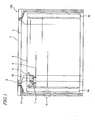
- FIG. 1 is a plan view schematically showing the general configuration of a liquid crystal module (a liquid crystal display device) in a first embodiment of the present invention.
- the liquid crystal module 100 in the first embodiment includes an active matrix substrate 1 and a counter substrate 2.
- the active matrix substrate 1 and the counter substrate 2 are bonded together by a sealing material (not shown) with a predetermined gap kept by means of a photo spacer (a projecting structure) disposed in a pixel region.
- Liquid crystal is sealed in a space formed by the active matrix substrate 1, the counter substrate 2, and the sealing material.
- the active matrix substrate 1 has a pixel region 3 in which pixel electrodes 43 are arranged in a matrix, and gate drivers 4a and 4b disposed on both sides of the pixel region 3 (in the example shown in FIG. 1 , on both sides in a horizontal direction (a longitudinal direction)).
- a source wiring 5 and a gate wiring 6 are disposed so as to be mutually orthogonal.
- a thin film transistor (TFT) 7 is formed.
- the inner construction of the gate drivers 4a and 4b is not shown in FIG. 1 , it includes a switching element (a TFT 30 shown in FIG. 3 ) which is formed simultaneously with the production process of the TFT 7 in the pixel region 3.
- the gate drivers 4a and 4b are formed in a monolithic manner in the active matrix substrate 1.
- the gate electrode is connected to the gate wiring 6, the source electrode is connected to the source wiring 5, and the drain electrode is connected to the pixel electrode 43, respectively.
- a gate signal is applied from the gate drivers 4a and 4b to the gate electrode of the TFT 7 via the gate wiring 6, thereby controlling the ON/OFF state of the TFT 7.
- a data signal is applied from a source driver which is not shown via the source wiring 5.
- the active matrix substrate 1 is formed in such a manner that the length of the shorter side is larger than the length of the shorter side of the counter substrate 2.
- a terminal region 8 for inputting and outputting various signals between the active matrix substrate 1 and an external circuit is formed.
- each source wiring 5 is connected to a source driver (not shown) provided on the outside of the active matrix substrate 1 via a source driver connecting terminal formed in the terminal region 8.
- terminals of the terminal region 8 are not shown, but one terminal, or two or more terminals may be formed in the terminal region 8.
- FIG. 1 shows one exemplary formation of the main wirings 14, so that any other formation in which the number of main wirings is different can be adopted.
- the main wirings 14 are connected to the terminals of the terminal region 8.
- the main wirings 14 are formed from the same material as that of the source wiring 5 or the gate wiring 6 of the pixel region 3 and formed simultaneously with the source wiring 5 or the gate wiring 6.
- the sealing material is laid on the outside of the gate driver 4a (on the outer circumferential side of the substrate) so as to cover one or more of the main wirings 14.
- the region, positioned on the outside of the pixel region, in which the gate drivers 4a and 4b, the main wirings 14, the terminal region 8, and the like are arranged is referred to as a peripheral region in the present specification.
- FIG. 2 is an enlarged plan view showing the vicinity of the region A encircled by a dashed line in FIG. 1 .
- a plurality of main wirings 14a to 14d are arranged on the outside of the gate driver 4a (on the outer circumferential side of the substrate).
- a contact portion 42 with a gate wiring 12 (a first wiring: a wiring for supplying a source voltage and a signal to the gate driver 4a) connected to the gate driver 4a is provided.
- FIG. 3 is a cross-sectional view, taken along a line B-B shown in FIG. 2 , showing the sectional structure of the contact portion 42.
- FIG. 3 shows the sectional structure of the contact portion 42 in a simplified manner.
- the main wiring 14 preferably has a layered structure including a plurality of kinds of metal layers, but in FIG. 3 , the main wiring 14 is shown as a metal layer of a single layer in an abbreviated manner.
- the illustration of a passivation film or the like is omitted, for example.
- the degree of evenness of various films, the size ratio of structural members, and the like shown in FIG. 3 do not necessarily represent the actual conditions.
- the liquid crystal module 100 in the present embodiment has the configuration in which the active matrix substrate 1 and the counter substrate 2 are bonded together by the sealing material 40, and the liquid crystal 34 is sealed in the gap therebetween.
- the gap therebetween is maintained by a columnar or wall-like photo spacer (the projecting structure) having a uniform height provided in the pixel region 3.
- the photo spacer is generally formed by a resin or the like so as to overlap the source wiring 5 or the gate wiring 6, while avoiding an opening portion of the pixel. The detailed embodiment of the photo spacer will be described later with reference to FIG. 15 .
- the sealing material 40 As the material for the sealing material 40, a thermosetting resin can be used.
- the sealing material 40 additionally has photo-curing property. Because after the active matrix substrate 1 and the counter substrate 2 are positioned and bonded together, it is possible to temporarily harden the sealing material 40 by exposure to light, and then to finally harden the sealing material 40 by heating.
- a resin having such properties a mixed resin of an epoxy resin and an acrylic resin, or the like is available.
- a photo-curing resin may be used as the sealing material 40.
- the active matrix substrate 1 includes a glass substrate 11 and a gate wiring 12 (a first wiring) formed on the surface of the glass substrate 11.
- the gate wiring 12 is connected to a gate electrode of the TFT 30 in the gate driver 4a.
- the gate wiring 12 is formed from the same material as that of the gate wiring 6 in the pixel region 3 simultaneously with the gate wiring 6 by the process for forming the gate wiring 6.
- the gate wirings 6 and 12 have, for example, a three-layer structure of a titanium layer, an aluminum layer, and a titanium layer. The structure is not limited to this.
- the gate wirings 6 and 12 may be a single metal layer, or may be a metal layer having two layers or four or more layers.
- the gate wiring 12 is covered with an interlayer insulating film 13 (a first insulating layer).
- the interlayer insulating film 13 is also referred to as a gate insulating film, and a silicon nitride film may be suitably used.
- a main wiring 14 (14a to 14c: a second wiring) is provided on the interlayer insulating film 13.
- the main wirings 14a to 14c are formed from the same material as that of the source wiring 5 in the pixel region 3 simultaneously with the source wiring 5 by the process for forming the source wiring 5.
- the source wiring 5 and the main wirings 14a to 14c preferably have a two-layer structure in which an aluminum layer is layered on a titanium layer, but the structure is not limited to this.
- the source wiring 5 and the main wirings 14a to 14c may be a single metal layer, or a metal layer of three or more layers. Instead of aluminum, molybdenum or the like may be used, for example.
- a main wiring 14d of the active matrix substrate 1 is electrically connected to a common electrode (described later) of the counter substrate 2 via silver paste (not shown) provided at an appropriate location.
- an interlayer insulating film 18 (a second insulating layer) is provided on the main wiring 14 and the TFT 30, an interlayer insulating film 18 (a second insulating layer) is provided.
- a pixel electrode 43 formed from a transparent electrode film such as indium tin oxide (ITO) or the like, and an alignment film (not shown) to regulate the alignment of liquid crystal 34 are provided in the known modes.
- the counter substrate 2 includes a color filter (which is not illustrated in FIG. 3 ) disposed on a glass substrate 21, and further includes an overcoat film 22 for covering the color filter and a transparent electrode film 23.
- the electrode film 23 covers the entire surface of the counter substrate 2 and functions as the common electrode.
- an alignment film (not shown) to regulate the alignment of the liquid crystal 34 is provided.
- a light blocking layer (a black matrix) 24 is provided in order to prevent the characteristics of the TFT 30 in the gate driver 4a from being deteriorated by light.
- a through hole (a contact hole) 20 which is formed through the interlayer insulating film 18 and the interlayer insulating film 13 on the main wiring 14c is provided.
- the electrode film 19 is continuously layered on the interlayer insulating film 18 in the contact portion 42, on wall faces of the interlayer insulating film 13, the main wiring 14c and the interlayer insulating film 18 in the through hole 20, and on the gate wiring 12 exposed in the bottom portion of the through hole 20.
- the electrode film 19 shown in FIG. 3 is formed from the same material as that of the pixel electrode 43 (ITO, for example) in the pixel region 3 simultaneously with the pixel electrode 43.
- the structural element indicated by the reference numeral 27 in FIG. 3 is a lower semiconductor layer
- the structural element indicated by the reference numeral 28 is an upper semiconductor layer.
- the lower semiconductor layer 27 and the upper semiconductor layer 28 can be, for example, formed simultaneously when the semiconductor layer of the TFT 30 is formed. In the case where the lower semiconductor layer 27 and the upper semiconductor layer 28 are exposed in the through hole 20, the electrode film 19 is formed on the wall faces of these layers.
- a conduction preventing member 31a formed by an insulating resin is formed on the electrode film 23 of the counter substrate 2 in the contact portion 42 shown in FIG. 3 , and a conduction preventing member 31b is formed on the inner side (on the side closer to the TFT 30) of the contact portion 42.
- the reference numerals 31a and 31b are used.
- the reference numeral 31 is used.
- the conduction preventing member 31 is a different structure from the sealing material 40.
- an alignment film (not shown) extended from the pixel region 3 may be interposed between the electrode film 23 and the conduction preventing member 31 between the electrode film 23 and the conduction preventing member 31, an alignment film (not shown) extended from the pixel region 3 may be interposed. It is necessary to provide the conduction preventing member 31 in the condition where at least part of the conduction preventing member 31 overlaps the electrode film 19 of the active matrix substrate 1 in the normal direction of the substrate surface (in the direction perpendicular to the substrate surface) (when viewed from the normal direction of the substrate surface).
- the conduction preventing member 31a is provided so as to overlap the entire surface of the electrode film 19 in the normal direction of the substrate surface, and the conduction preventing member 31b is provided in a position which does not overlap the electrode film 19.
- the conduction preventing member 31b in the position which does not overlap the electrode film 19 can be omitted, and the conduction preventing member 31a does not necessarily overlap the entire surface of the electrode film 19.
- the conduction preventing members 31a and 31b are shown, but the number of conduction preventing members is not limited to this.
- the conduction preventing member 31 is formed in a columnar shape or a wall-like shape by using the same material as that of the projecting structure (the photo spacer herein) provided in the pixel region 3.
- the conduction preventing member 31 and the photo spacer can be simultaneously formed by a photolithography process by using a material of transparent photosensitive acrylic resin, for example.
- an end face of the conduction preventing member 31a on the side of the active matrix substrate 1 has a width and a length sufficient for at least covering the electrode film 19 in the contact portion 42.
- the conduction preventing member 31a is disposed so as to be projected from the surface of the electrode film 23 of the counter substrate 2.
- the conduction preventing member 31a lies between these substrates with no space interposed therebetween.
- the conduction preventing member 31 also has an effect functioning as the photo spacer to define the cell gap in the pixel region 3. Accordingly, in the case where the conduction preventing member 31 is formed from the same material as that of the photo spacer to define the cell gap, as shown in FIG. 3 , the conduction preventing member 31b is preferably formed in a portion other than the contact portion 42 on the outside of the pixel region 3. With such a configuration, it is possible to attain an effect that the conduction preventing member 31b keeps the gap between the active matrix substrate 1 and the counter substrate 2 uniform on the outside of the pixel region 3.
- the conduction preventing member 31 is formed from the same material as that of the photo spacer to maintain the predetermined gap between the active matrix substrate 1 and the counter substrate 2 in the pixel region 3 simultaneously with the photo spacer.
- the conduction preventing member 31 can advantageously be formed without increasing the number of production processes.
- an alignment regulating structure to regulate the alignment condition of liquid crystal may be provided as the projecting structure provided in the pixel region 3, other than the photo spacer to define the gap between the substrates.
- the alignment regulating structure is used, for example, in a vertical alignment type liquid crystal module, or the like.
- the alignment regulating structure is formed in a wall-like shape having a predetermined height by using a transparent resin.
- the conduction preventing member 31 can be formed from the same material as that of the alignment regulating structure, unlike the photo spacer to define the gap between the substrates.
- the conduction preventing member 31 can be formed from a material different from that of the photo spacer, and can be formed by a process different from the process of the photo spacer. In addition, the conduction preventing member 31 can be formed from a material different from that of the alignment regulating structure, and can be formed by a process different from the process of the alignment regulating structure.
- the conduction preventing member 31 is formed on the common electrode (the electrode film 23) of the counter substrate 2 so as to at least partially overlap the electrode film 19 on the outside of the pixel region 3 of the active matrix substrate 1 in the normal direction of the substrate surface.
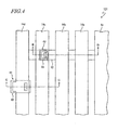
- FIG. 4 is an enlarged plan view showing the vicinity of a region corresponding to the region A encircled by the dashed line in FIG. 1 in a liquid crystal display device (a liquid crystal module) 101 in the second embodiment.
- the general configuration of the liquid crystal display device 101 is fundamentally the same as that of the liquid crystal display device 100 shown in FIG. 1 .
- a conductive portion 41 to obtain electrical conduction between the active matrix substrate 1 and the counter substrate 2 is provided on the main wiring 14d.
- the sealing material 40 contains a conductive particulate matter (described later), and by the provision of the sealing material 40 in the conductive portion 41, electrical conduction between the active matrix substrate 1 and the counter substrate 2 can be obtained via the conductive particulate matter. Accordingly, the silver paste included in the configuration of the first embodiment is not required, and the area of the frame region can be advantageously reduced as compared with the first embodiment.
- the conductive portion 41 may be provided on the main wiring 14d in the frame portion closer to the terminal region 8 or in the frame portion on the opposite side to the terminal region 8.
- the contact portion 42 with the gate wiring 12 connected to the gate driver 4a is provided on the main wiring 14c.
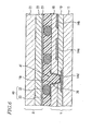
- FIG. 5 is a cross-sectional view, taken along a line B-B shown in FIG. 4 , showing the sectional structure of the contact portion 42.
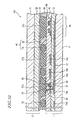
- FIG. 6 is a cross-sectional view, taken along a line C-C shown in FIG. 4 , showing the sectional structure of the conductive portion 41.
- FIG. 5 and FIG. 6 show the sectional structures of the conductive portion 41 and the contact portion 42 in a simplified manner.
- the main wiring 14 has a layered structure of a plurality of kinds of metal layers.
- the main wiring 14 is shown as a single metal layer in the abbreviated manner.
- the illustration of the passivation film or the like is omitted, for example.
- the degrees of evenness of various films, the size ratio of the structural members, and the like do not necessarily represent the actual conditions.
- the liquid crystal module (the liquid crystal display device) 101 in the present embodiment has the configuration in which the active matrix substrate 1 and the counter substrate 2 are bonded together by the sealing material 40, and the liquid crystal 34 are sealed in the gap between the substrates.
- the gap between them is kept uniform by a photo spacer (a projecting structure) provided in the pixel region 3.
- a photo spacer a projecting structure
- thermosetting resin 33 As for the sealing material 40, a conductive particulate matter 32 is contained in a thermosetting resin 33 as a base material.
- the thermosetting resin 33 also has a photo-curing property, preferably. Because, after the active matrix substrate 1 and the counter substrate 2 are positioned and then bonded together, the sealing material 40 can be temporarily hardened by exposure to light, and then the sealing material 40 can be finally hardened by heating.
- a resin having such properties a mixed resin of an epoxy resin and an acrylic resin or the like is available.
- a transparent resin may be used as the thermosetting resin 33, a black resin may sometimes be preferable as in a modified example (the fifth modified example) which will be described later.
- the conductive particulate matter 32 for example, plastic beads are plated with a conductive metal (for example, gold plating, or the like).
- the conductive particulate matter 32 has a substantially spherical form before being mixed into the thermosetting resin 33, but it is preferred that the conductive particulate matter 32 may have a plastic property to a degree with some collapse but without being broken in the bonding process of the active matrix substrate 1 and the counter substrate 2.
- a thermoplastic resin such as an epoxy resin or the like may preferably be used, for example.
- the conductive particulate matter 32 can be interposed between the active matrix substrate 1 and the counter substrate 2 without being broken.
- the shape of the conductive particulate matter 32 is not limited to the substantially spherical form, but may be an ovoid shape (substantially ellipse in section), or a columnar shape. Alternatively, the conductive particulate matter 32 may be a particulate matter having a shape of quadrangle, polygon, or a different complicated shape in section.
- the main wiring 14 (14a to 14c) are provided on the interlayer insulating film 13.
- the main wirings 14a to 14c are formed from the same material as that of the source wiring 5 in the pixel region 3 simultaneously with the source wiring 5 by the process of forming the source wiring 5.
- the main wiring 14d is formed from the same material as that of the gate wiring 6 under the interlayer insulating film 13 simultaneously with the gate wiring 6 by the process of forming the gate wiring 6.
- a through hole (a contact hole) 20 is formed in the interlayer insulating film 13 on the main wiring 14d and the interlayer insulating film 18.
- the main wiring 14d is electrically connected to the electrode film 19 on the interlayer insulating film 18.
- the electrode film 19 is continuously layered on the interlayer insulating film 18 in the conductive portion 41, on the wall faces of the interlayer insulating films 13 and 18 in the through hole 20, and on the main wiring 14d exposed in the bottom portion of the through hole 20.
- the sealing material 40 is provided in a position which covers the main wirings 14a to 14d, or provided over a part of or all of the main wirings 14a to 14d.
- the electrode film 19 of the conductive portion 41 is made to be electrically conductive to an electrode film 23 of the counter substrate 2 by means of the conductive particulate matter 32 in the sealing material 40. Accordingly, a signal input from a terminal of the terminal region 8 to the main wiring 14d is supplied to the common electrode of the counter substrate 2 via the electrode film 19 and the conductive particulate matter 32.
- the through hole 20 is formed through the interlayer insulating film 18 on the main wiring 14c and the interlayer insulating film 13, and the main wiring 14c and the gate wiring 12 are electrically connected via the through hole 20 and the electrode film 19. That is, the electrode film 19 is continuously layered on the interlayer insulating film 18 in the contact portion 42, on the wall faces of the interlayer insulating film 13, the main wiring 14c, and the interlayer insulating film 18, and on the gate wiring 12 exposed in the bottom portion of the through hole 20. In the case where a lower semiconductor layer 27 and an upper semiconductor layer 28 are exposed in the through hole 20, the electrode film 19 is also formed on the wall faces of these layers.
- the electrode film 19 respectively shown in FIG. 5 and FIG. 6 is formed from the same material (e.g., ITO) as that of the pixel electrode 43 in the pixel region 3 simultaneously with the pixel electrode 43.
- a conduction preventing member 31 (31a, 31b) formed from an insulating resin is provided on the electrode film 23 of the counter substrate 2.
- the conduction preventing member 31 is buried in the sealing material 40 in the example shown in FIG. 5 (or surrounded by the sealing material 40), but the conduction preventing member 31 is a separate structural member from the sealing material 40.
- an alignment film (not shown) extended from the pixel region 3 may be interposed. It is necessary to provide the conduction preventing member 31 so as to at least partially overlap the electrode film 19 of the active matrix substrate 1 in the normal direction of the substrate surface.
- the conduction preventing member 31a is provided so as to overlap the entire of the electrode film 19 in the normal direction of the substrate surface, and the conduction preventing member 31b is provided in a position which does not overlap the electrode film 19.
- the conduction preventing member 31b may be omitted, and the conduction preventing member 31a does not necessarily overlap the entire of the electrode film 19.
- the conduction preventing member 31 is formed in a columnar or wall-like shape by using the same material as that of the projecting structure (the photo spacer herein) provided in the pixel region 3.
- the conduction preventing member 31 and the photo spacer can be formed simultaneously by photolithography by using, for example, a transparent photosensitive acrylic resin as the material.
- the end face of the conduction preventing member 31a on the side of the active matrix substrate 1 may have a width and a length sufficient for covering at least the electrode film 19 of the contact portion 42.
- the conduction preventing member 31a is provided so as to protrude from the surface of the electrode film 23 of the counter substrate 2.
- the conduction preventing member 31a is interposed between the substrates with no space. Accordingly, in the contact portion 42, there is no space into which the sealing material 40 enters between the electrode film 19 of the active matrix substrate 1 and the common electrode (the electrode film 23) of the counter substrate 2. Accordingly, with such a configuration, in the contact portion 42, it is possible to prevent a situation that the conductive particulate matter 32 in the sealing material 40 causes short circuit between the active matrix substrate 1 and the counter substrate 2 from occurring.
- FIG. 19 shows a configuration in which the conduction preventing member 31 is omitted from the liquid crystal module 101 in the present embodiment (a liquid crystal module 901).
- the liquid crystal module 901 in the comparative example has the same configuration as that of the liquid crystal module 101 in the present embodiment except for the absence of the conduction preventing member 31.
- the conductive particulate matter 32 contained in the sealing material 40 is interposed between the electrode film of the active matrix substrate 1 and the electrode film 23 of the counter substrate 2. This may possibly cause short circuit between the active matrix substrate 1 and the counter substrate 2.
- the problem of short circuit between the active matrix substrate 1 and the counter substrate 2 by the conductive particulate matter 32 can be solved by the provision of the conduction preventing member 31.
- the conduction preventing member 31 also attains the effect that it has the similar function as a photo spacer to define a cell gap in the pixel region 3. Accordingly, in the case where the conduction preventing member 31 is formed from the same material as that of the photo spacer to define the cell gap, as shown in FIG. 5 , it is preferred to adopt a configuration in which the conduction preventing member 31b is also provided in a position other than the contact portion 42 on the outside of the pixel region 3. With such a configuration, it is possible to attain such an effect that the conduction preventing member 31b may keep the space between the active matrix substrate 1 and the counter substrate 2 on the outside of the pixel region 3 uniform.
- the conduction preventing member 31 is preferably formed from the same material as that of the photo spacer to maintain a predetermined gap between the active matrix substrate 1 and the counter substrate 2 in the pixel region 3, simultaneously with the photo spacer. In this case, the conduction preventing member 31 can be advantageously formed without increasing the number of production process steps.
- an alignment regulating structure to define the alignment condition of liquid crystal may sometimes be included.
- the alignment regulating structure will be described later with reference to FIG. 16 .
- the conduction preventing member 31 can be formed from the same material as that of the alignment regulating structure, instead of the photo spacer to define the gap between the substrates.
- the conduction preventing member 31 may be formed from a material different from that of the above-mentioned photo spacer, and may be formed by a process step different from the step of forming the photo spacer.
- the conduction preventing member 31 may be formed from a material different from that of the above-mentioned alignment regulating structure, and may be formed by a process step different from the step of forming the alignment regulating structure.
- the conduction preventing member 31 is provided on the common electrode (the electrode film 23) of the counter substrate 2 so as to at least partially overlap the electrode film 19 on the outside of the pixel region of the active matrix substrate 1 in the normal direction of the substrate surface. Accordingly, even in the case where the sealing material 40 is disposed in a region in which the electrode film 19 is formed, the conductive particulate matter 32 contained in the sealing material 40 is prevented from entering between the electrode film 19 of the active matrix substrate 1 and the electrode film 23 of the counter substrate 2. Accordingly, it is possible to prevent short circuit between the active matrix substrate 1 and the counter substrate 2 in the contact portion 42 from occurring.
- Fig. 7 is a cross-sectional view showing a general configuration of a first modified example of the liquid crystal module 101 in the second embodiment.
- a glass fiber (a spacer in seal) 35 which is cut into short pieces is mixed in the sealing material 40 together with the conductive particulate matter 32.
- the glass fiber 35 has a columnar shape, and its diameter in section is smaller than that of the conductive particulate matter 32.
- the glass fiber 35 does not deform when the active matrix substrate 1 and the counter substrate 2 are bonded together.
- the glass fiber 35 is harder than the conductive particulate matter 32, and has higher elastic modulus.
- the diameter in section of the glass fiber 35 defines the minimum gap between the active matrix substrate 1 and the counter substrate 2 in the portion in which the sealing material 40 is provided. It is preferred that the diameter (the diameter at least before the deformation or the diameter of the widest portion after the deformation) of the conductive particulate matter 32 is a little larger than the minimum gap (i.e., the diameter in section of the glass fiber 35).
- the diameter before the deformation or the diameter of the longest portion of the conductive particulate matter 32 is preferably larger than the diameter in section of the glass fiber 35 in the range of about 4 to 5 ⁇ m.
- the diameter of the conductive particulate matter 32 is preferably about 4 ⁇ m.
- the conductive particulate matter 32 As described above, as the conductive particulate matter 32, the particulate matter having a diameter which is a little larger than the diameter in section of the glass fiber 35 is used, so that both of the electrode film 19 of the active matrix substrate 1 and the electrode film 23 of the counter substrate 2 are surely in contact with a single conductive particulate matter 32 in the conductive portion 41. Accordingly, in the conductive portion 41, electrical conduction between the active matrix substrate 1 and the counter substrate 2 can be surely obtained.
- the glass fiber 35 since the glass fiber 35 is mixed in the sealing material 40, the glass fiber 35 performs a function equivalent to the photo spacer to define the cell gap in the pixel region 3. Accordingly, it is possible to attain the effect that the gap between the active matrix substrate 1 and the counter substrate 2 is kept uniform on the outside of the pixel region 3.
- the columnar glass fiber 35 is used as the spacer in seal.
- spherical rigid plastic beads may be used.
- the plastic beads in this case have a diameter which is a little smaller than that of the conductive particulate matter 32 and have a higher degree of rigidity than the conductive particulate matter 32.
- FIG. 8 is a cross-sectional view showing a general configuration of a second modified example of the liquid crystal module 101.
- the second modified example of the liquid crystal module 101 has a conduction preventing member 36 (36a, 36b), instead of the above-described conduction preventing member 31.
- the reference numerals 36a and 36b are used, and if the conduction preventing members 36a and 36b are commonly described, the reference numeral 36 is used.
- the conduction preventing member 36 is disposed so as to protrude from the counter substrate 2, but the height of the conduction preventing member 36 is smaller than the magnitude of the cell gap between the active matrix substrate 1 and the counter substrate 2 (i.e., the height of the photo spacer in the pixel region 3).
- the height of the conduction preventing member 36 preferably satisfies the condition (a) that when the active matrix substrate 1 and the counter substrate 2 are bonded together by the sealing material 40, the end face of the conduction preventing member 36 will not be in contact with the electrode film 19.
- the condition (a) the end face of the conduction preventing member 36 is not strongly in contact with the electrode film 19 when the substrates are bonded together. As a result, contact failure caused by the rupture of electrode film 19 can be prevented.
- the height of the conduction preventing member 36 is more preferably determined by the second condition (b) that even if the conductive particulate matter 32 enters between the end face of the conduction preventing member 36 on the side of the active matrix substrate 1 and the electrode film 19, the gap between the active matrix substrate 1 and the counter substrate 2 is not affected, in addition to the condition (a).
- the gap between the active matrix substrate 1 and the counter substrate 2 can be kept uniform.
- the height of the photo spacer (or the cell gap) of the pixel region 3 is different from the height of the conduction preventing member 36.
- the conduction preventing member 36 can be simultaneously formed from the same material as that of the photo spacer in the pixel region 3.
- the positive-type photosensitive acrylic resin has a characteristic that the depth of recessed portion formed by etching is varied depending on the amount of exposure.
- the positive-type photosensitive acrylic resin is applied on the electrode film 23 of the counter substrate 2, and a photo mask (a so-called halftone mask) in which films having mutually different transmittances are partially arranged or a slit is provided is used, both of the conduction preventing member 36 and the photo spacer can be formed simultaneously so as to have mutually different thicknesses by using the single mask.
- a photo mask a so-called halftone mask
- both of the conduction preventing member 36 and the photo spacer can be formed simultaneously so as to have mutually different thicknesses by using the single mask.
- an alignment regulating structure to define the alignment condition of liquid crystal may sometimes be included in the pixel region 3.
- the height of the alignment regulating structure is generally lower than the height of the photo spacer to define the cell gap.
- the conduction preventing member 36 is preferably formed by using the same material as that of the alignment regulating structure, so as to have the same height.
- the configuration in which both of the conduction preventing member 36a provided in the contact portion 42 and the conduction preventing member 36b provided in the portion other than the contact portion 42 are formed so as to be lower than the cell gap is exemplarily shown.
- the heights of the conduction preventing member 36a and the conduction preventing member 36b are not necessarily equal.
- the conduction preventing member 36b may be formed from the same material as that of the photo spacer so as to have the same height
- the conduction preventing member 36a may be formed from the same material as that of the alignment regulating structure so as to have the same height.
- the conduction preventing member 36 may be formed from a material different from that of the photo spacer, and may be formed in a process step different from that of the photo spacer.
- the conduction preventing member 36 may be formed from a material different from that of the alignment regulating structure, and may be formed in a process step different from that of the alignment regulating structure.
- FIG. 8 the example in which the glass fiber 35 is mixed in the sealing material 40 is exemplarily shown.
- the glass fiber 35 is not necessarily required in the second modified example.
- the modified example of the liquid crystal module 101 in the second embodiment is described.
- the liquid crystal module 100 in the first embodiment it is possible to include the conduction preventing member 36 instead of the conduction preventing member 31. With such a configuration, the same effects can be attained.
- FIG. 9 is a cross-sectional view showing a general configuration of a third modified example of the liquid crystal module 101.
- the third modified example of the liquid crystal module 101 has the configuration in which concave and convex are provided on an end face of the conduction preventing member 36 in the second modified example on the side of the active matrix substrate 1.
- the concave and convex on the end face of the conduction preventing member 36 can be realized by providing a plurality of small regions with mutually different light transmittances in a photo mask corresponding to the end face when the conduction preventing member 36 is patterned by photolithography.
- a mask portion with lower light transmittance may be assigned to a portion of the end face of the conduction preventing member 36 to be the convex portion, and a mask portion with higher light transmittance may be assigned to a portion to be the concave portion.
- the concave and convex of the end face of the conduction preventing member 36 are formed roughly and deeply as much as possible. With such a configuration, even if the thermosetting resin 33 or the conductive particulate matter 32 of the sealing material 40 enters between the end face of the conduction preventing member 36 and the active matrix substrate 1 when the active matrix substrate 1 and the counter substrate 2 are bonded together, the entered substance can be absorbed in the concave portion. As a result, even if the sealing material 40 enters between the end face of the conduction preventing member 36 and the active matrix substrate 1, it is difficult for the gap between the active matrix substrate 1 and the counter substrate 2 to vary, so that the gap between the substrates can be maintained to be a desired value.
- FIG. 9 the example in which the glass fiber 35 is mixed in the sealing material 40 is shown, but the glass fiber 35 is not necessarily required in the third modified example.
- the concave and convex may be formed on an end face (an end face on the side of the active matrix substrate 1 or on the side of the counter substrate 2) of the conduction preventing member 31 having substantially the same height as that of the cell gap (see the first modified example) in the normal direction of substrate surface.
- FIG. 10 is a cross-sectional view showing a general configuration of a fourth modified example of the liquid crystal module 101.
- a conduction preventing member 37 (37a to 37c) which is colored to black so as not to transmit light is provided.
- the reference numerals 37a to 37c are used, but in the case where the conduction preventing members 37a to 37c should be commonly described, the reference numeral 37 is used.
- the conduction preventing member 37 can be produced by a photosensitive acrylic resin which is colored to black.
- the conduction preventing member 37 can be formed from the same material and by the same process step as those of the photo spacer in the pixel region 3.
- the conduction preventing member 37 may be alternatively formed from a material different from that of the photo spacer, and may be formed by a process step different from that of the photo spacer.
- the conduction preventing member 37c (the second conduction preventing member) above the TFT 30 of the gate driver 4a, the light blocking layer 24 of the counter substrate 2 (see FIG. 3 ) is not required.
- the conduction preventing member 37c does not necessarily cover the entire of the TFT 30, but it is sufficient that the conduction preventing member 37c acts so that light is not incident at least on the channel region.
- the glass fiber 35 may be mixed in the sealing material 40.
- the conduction preventing member 37 may be used instead of the conduction preventing member 31 of the liquid crystal module 100 in the first embodiment. With such a configuration, the same effects can be attained.
- FIG. 11 is a cross-sectional view showing a general configuration of a fifth modified example of the liquid crystal module 101.
- the fifth modified example of the liquid crystal module 101 is different from the forth modified example in that as the base material of the sealing material 40, a thermosetting resin 38 colored to black is used instead of the transparent thermosetting resin 33.
- the black conduction preventing member 37c above the TFT 30 of the gate driver 4a, the light blocking layer 24 on the side of the counter substrate 2 (see FIG. 3 ) is not required.
- the conduction preventing member 37c does not necessarily cover the entire of the TFT 30, but it is sufficient that the conduction preventing member 37c may be positioned so that light is not incident at least on the channel region.
- the sealing material 40 may be extended above the TFT 30.
- the channel region of the TFT 30 is covered with the black thermosetting resin 38, so that it is possible to prevent the characteristic deterioration of the TFT 30 without the light blocking layer 24 of the counter substrate 2.
- the width of the sealing material 40 is larger than the width of the main wiring region, the area of the frame region can be advantageously reduced, not by causing the sealing material to protrude on the outside of the main wiring region, but by forming the sealing material 40 above the gate driver 4a.
- the glass fiber 35 may be mixed in the sealing material 40.
- FIG. 12 is a cross-sectional view showing a general configuration of the sixth modified example of the liquid crystal module 101.
- the sixth modified example of the liquid crystal module 101 is characterized in that the conduction preventing member 39 (39a, 39b) is provided not on the side of the counter substrate 2 but on the side of the active matrix substrate 1. Specifically, before the active matrix substrate 1 and the counter substrate 2 are bonded together, the conduction preventing member 39 is formed on the side of the active matrix substrate 1.
- the photo spacer of the pixel region 3 is also provided on the side of the active matrix substrate 1, and the conduction preventing member 39 is preferably formed simultaneously by using the same material as that of the photo spacer of the pixel region 3.
- the conduction preventing member 39 may be formed from a material different from that of the photo spacer, and may be formed by a different process step from that of the photo spacer.
- the glass fiber 35 may be mixed in the sealing material 40 (see the first modified example).
- the height of the conduction preventing member 39 may be smaller than the cell gap (see the second modified example).
- the end face of the conduction preventing member 39 on the side of the counter substrate 2 may have concave and convex (see the third modified example).
- the conduction preventing member 39 may be colored to black (see the fourth modified example), and the employed sealing material 40 may include a black thermosetting resin as its base material (see the fifth modified example).
- the conduction preventing member 39 may be used instead of the conduction preventing member 31 in the liquid crystal module 100 of the first embodiment. With such a configuration, the same effects can be attained.
- liquid crystal display device 101 in the second modified example of the second embodiment shown in FIG. 8 is exemplarily described. That is, in the example described below, the conduction preventing member 36 having the height smaller than the cell gap is provided on the side of the counter substrate 2. In addition, the glass fiber 35 is mixed in the sealing member 40 (see FIG. 8 ), but this is not essential.
- FIG. 13 is a cross-sectional view showing the configuration in the vicinity of the conductive portion 41 (see FIG. 4 ) in the liquid crystal display device 101 of the second modified example in more detail.
- FIG. 14 is a cross-sectional view showing the configuration in the vicinity of the contact portion 42 also in the second modified example in more detail.
- FIG. 15 illustrates the configuration of a section taken along a line D-D shown in FIG. 1 (the sectional configuration of a pixel).
- the main wiring 14d in the present embodiment has a three-layer structure including a titanium layer 141d as a lower layer, an aluminum layer 142d as a middle layer, and a titanium layer 143d as an upper layer.
- the gate wiring 6 in the pixel region 3 which is simultaneously formed with the main wiring 14d has the same structure as that of the main wiring 14d.
- the electrode film 19 is formed by ITO similarly to the pixel electrode 43 in the pixel region 3.
- the interlayer insulating film 13 and a passivation film 143 formed on the interlayer insulating film 13 are provided on the active matrix substrate 1, as shown in FIG. 13 .
- the passivation film 143 is a silicon nitride film which can attain such effects that the characteristic deterioration of active elements is prevented.
- the interlayer insulating film 18 of a photosensitive acrylic resin is provided above the passivation film 143.
- the thickness of the interlayer insulating film 18 is about 2 to 4 ⁇ m in the thickest position.
- the gate wiring 12 has a three-layer structure in which a titanium layer, an aluminum layer, and a titanium layer are successively layered, which are omitted in the figure.
- the gate wiring 6 in the pixel region 3 which is simultaneously formed with the gate wiring 12 has the same structure as that of the gate wiring 12.
- the interlayer insulating film 13 a silicon nitride film may be used.
- the main wiring 14c has a two-layer structure including a titanium layer 141c as a lower layer and an aluminum layer 142c as an upper layer, and is formed by the same process step as that of the source wiring 5 in the pixel region 3.
- the contact portion 42 has, as shown in the figure, a region in which the gate wiring 12, the interlayer insulating film 13, and an amorphous silicon film 146 are laminated between the glass substrate 11 and the electrode film 19.
- the contact portion 42 also has a region in which the gate wiring 12, the interlayer insulating film 13, the amorphous silicon film 146, and the titanium layer 141c are laminated between the glass substrate 11 and the electrode film 19, and a region in which the gate wiring 12, the interlayer insulating film 13, the titanium layer 141c, the aluminum layer 142c, the passivation film 143, and the interlayer insulating film 18 are laminated between the glass substrate 11 and the electrode film 19.
- the upper layer (i.e., the aluminum layer 142c) of the main wiring 14c is removed by etching, so that the titanium layer 141c is in contact with the electrode film 19.
- the passivation film 143 is a silicon nitride film.
- the interlayer insulating film 18 of a photosensitive acrylic resin is provided on the passivation film 143.
- the interlayer insulating film 18 has the thickness of about 2 to 4 ⁇ m in the thickest portion thereof.
- the electrode film 19 is electrically in contact with the titanium layer 141c of the main wiring 14c and the gate wiring 12 in the through hole 20 (hereinafter also referred to as a contact hole 20).
- a stepped portion 144 is provided in the contact hole 20 of the interlayer insulating film 18, and a gently sloping face 145 is formed between the open end of the contact hole 20 and the stepped portion 144.
- the stepped portion 144 is a portion which is formed at a lower level than the uppermost surface of the interlayer insulating film 18.
- the electrode film 19 is extended from the bottom portion of the contact hole 20 to the middle of the stepped portion 144.
- the end portion of the electrode film 19 is positioned on the stepped portion 144, and does not reach the sloping face 145 and the surface of the interlayer insulating film 18, so that it is possible to surely secure the distance between the electrode film 19 and the electrode film 23 of the counter substrate. Accordingly, there is an advantage that short circuit between the electrode film 19 of the active matrix substrate 1 and the electrode film 23 of the counter substrate 2 can be prevented.
- the passivation film 143 and the interlayer insulating film 18 are interposed between the main wiring 14c and the electrode film 19, it is possible to prevent electrolytic corrosion of the ITO as the electrode film 19 and the aluminum layer 142c of the main wiring 14c.
- the margin for positioning precision in bonding or the like can be enlarged as compared with the case where the contact hole 20 has a steep or vertical inner wall.
- the thickness of the conduction preventing member 36 is determined so that the thickness does not substantially vary the gap between the active matrix substrate 1 and the counter substrate 2 even when the conductive particulate matter 32 enters between the end face of the conduction preventing member 36 on the side of the counter substrate 2 and the electrode film 19, as described above.
- the thickness of the interlayer insulating film 18 is about 2.5 ⁇ m in the thickest portion thereof, the diameter in section of the glass fiber 35 is about 3 ⁇ m, and the diameter of the conductive particulate matter 32 is about 4 ⁇ m, the sum of the thickness of the interlayer insulating film 18 and the diameter in section of the glass fiber 35 is about 5.5 ⁇ m.
- the height of the conduction preventing member 36 is smaller than about 1.5 ⁇ m. In this case, the height of the conduction preventing member 36 is about 1.0 ⁇ m.
- FIG. 15 is a cross-sectional view taken along a line D-D shown in FIG. 1 .
- the photo spacer 53 to regulate the cell gap is formed above the source wiring 5.
- a black matrix (BM) 149 is provided above the photo spacer 53.
- the black matrix 149 is provided on the boundary among a red color filter 150R, a green color filter 150G, and a blue color filter 150B, so as to overlap the photo spacer 53 and the source wiring 5 blow the photo spacer 53.
- the red color filter 150R, the green color filter 150G, and the blue color filter 150B are disposed so as to overlap the region in which the pixel electrode 43 is provided (the pixel opening portion), respectively.
- the thickness of the black matrix 149 is about 1 ⁇ m
- the thickness of each of the red color filter 150R, the green color filter 150G, and the blue color filter 150B is about 2 ⁇ m
- the thickness of the overcoat film 22 on the color filters is about 0.5 ⁇ m.
- the source wiring 5 of the pixel region 3 has a layered structure of a titanium layer 51 and an aluminum layer 52, similarly to the afore-mentioned main wiring 14.
- the passivation film 143 is layered.
- the interlayer insulating film 18 of a photosensitive acrylic resin is layered.
- the thickness of the interlayer insulating film 18 is about 2.5 ⁇ m in the thickest portion thereof.
- the surface of the interlayer insulating film 18 is substantially even.
- the glass substrate 21, the color filters 150R, 150G, and 105B of respective colors, the black matrix 149, the overcoat film 22, and the electrode film 23 are layered in this order.
- the electrode film 23 is a common electrode formed by ITO.
- the thickness of the electrode film 23 is about 0.1 ⁇ m.
- a photo spacer 53 of a photosensitive acrylic resin is formed on the electrode film 23, a photo spacer 53 of a photosensitive acrylic resin is formed.
- the alignment film 148 is formed so as to cover the electrode film 23 and the photo spacer 53.
- the thicknesses of the alignment films 147 and 148 are about 100 nm, respectively.
- the line width of one source wiring 5 is about 2 to 3 ⁇ m, and the line widths of the photo spacer 53 and the black matrix 149 which overlap the source wiring 5 are also about 2 to 3 ⁇ m.
- the height of the photo spacer 53 is about 3 ⁇ m. This is substantially equal to the diameter in section of the glass fiber 35 to define the thickness of the sealing material 40.
- the conduction preventing member in the region on the outside of the pixel region is preferably formed by using the same material and by the same process step as those of the photo spacer 53, thereby simplifying the production process.
- an alignment regulating structure to define the alignment condition of liquid crystal may sometimes be formed other than the photo spacer to define the gap between the substrates.
- the alignment regulating structure is used, for example, in a vertical alignment type liquid crystal module, or the like.
- a specific exemplary configuration of the alignment regulating structure will be described with reference to FIG. 16 .
- an alignment regulating structure 81 is formed as a projecting structure which is lower than the photo spacer 53 in a pixel region of a vertical alignment type liquid crystal module.
- alignment films 147 and 148 are vertical alignment films to cause the liquid crystal molecules to align vertically with respect to the substrate surface.
- the alignment regulating structure 81 is provided on the side of the counter substrate 2 in the vicinity of the center of each pixel, so as to cause the liquid crystal molecules 341 around it to radially align in an inclination manner.
- the alignment regulating structure 81 is formed on the electrode film 23 similarly to the photo spacer 53. Accordingly, the surface of the alignment regulating structure 81 is covered with the vertical alignment film 148. With such a configuration, due to the anchoring effect of the vertical alignment film 48 provided on an inclined surface 81s of the alignment regulating structure 81, the liquid crystal molecules 341 are aligned substantially vertically with respect to the inclined surface 81s .
- the alignment regulating structure 81 is formed so as to have a truncated cone shape.
- the shape may be selected from various shapes such as a cone or a triangular pyramid.
- the conduction preventing member 31 may be formed from the same material and by the same process step as those of the alignment regulating structure 81, thereby advantageously simplifying the production process.
- FIG. 17 is a plan view schematically showing the configuration of the TFT 30 in the gate driver 4a and the contact portion 63 arranged in the vicinity thereof.
- FIG. 18 is a cross-sectional view taken along a line E-E shown in FIG. 17 .
- the configuration of the gate driver 4a is described, but the gate driver 4b may also have the same configuration.
- the TFT is a comb-shaped TFT, but a switching element in the gate driver 4a is not limited to this.
- an interlayer insulating film 13 is provided on the gate wiring 12, and a silicon layer 15 of n + silicon or the like, a drain wiring 61, a source wiring 62, and the like are formed thereon.
- the drain wiring 61 and the source wiring 62 are wirings formed in the gate driver 4a from the same material as that of the main wiring 14 and the source wiring 5 in the pixel region 3 simultaneously with the source wiring 5.
- the main wiring 14, the drain wiring 61, and the source wiring 62 have a two-layer structure of a titanium layer 141c and an aluminum layer 142c, for example.
- two electrodes extended from the drain wiring 61 constitute drain electrodes 61a and 61b of the TFT 30, and one electrode extended from the source wiring 62 constitutes the source electrode 62a.
- a passivation film 143 is layered on the drain wiring 61 and the source wiring 62.
- the interlayer insulating film 18 is layered on the passivation film 143.
- the through hole 20 is provided in the interlayer insulating film 18 and the interlayer insulating film 13.
- the electrode film 19 is continuously layered on the wall faces of the interlayer insulating film 13 and the interlayer insulating film 18 in the through hole 20, an exposed portion of the main wiring 14, and the gate wiring 12 exposed in the bottom portion of the through hole 20. With such a configuration, the gate wiring 12 and the main wiring 14 are electrically connected in the contact portion 63.
- the electrode film 19 is also formed on the exposed faces thereof.
- the sealing material 40 does not exist.
- the sealing material 40 contains a photosensitive resin as its base material, and the sealing material 40 is temporarily hardened with the radiation of light to the photosensitive resin in the production process.
- the irradiation of the TFT 30 with light may deteriorate the channel characteristics.
- the sealing material 40 is to be formed on the TFT 30, the TFT 30 is irradiated with light in the production process, so that there arises a problem that the characteristics of the TFT 30 are deteriorated.
- the sealing material 40 does not exist on or above the TFT 30, so that the deterioration in characteristics of the TFT 30 can be prevented.
- a light blocking layer 24 is formed above the gate drivers 4a and 4b.
- a conduction preventing member 36 is preferably provided on the counter substrate 2 above the contact portion 63.
- a conduction preventing member (corresponding to the above-mentioned conduction preventing member 31a) having the same height as that of the photo spacer to define the cell gap or the alignment condition of liquid crystal may be provided.
- a black conduction preventing member may be provided.
- the conduction preventing member 36 may be provided on the side of the active matrix substrate 1.
- the conduction preventing member 36 may be formed from a different material from that of the photo spacer, and formed by a different process step from that of the photo spacer. In addition, the conduction preventing member 36 may be formed from a different material from that of the above-mentioned alignment regulating structure, or formed by a different process step from that of the alignment regulating structure.
- a glass substrate 11 is first washed and dried up, a titanium layer, an aluminum layer, and a titanium layer are sequentially layered on the surface of the glass substrate 11 by sputtering.
- the three layers are shaped by photolithography and dry etching, thereby forming a gate wiring 12 (a first wiring).
- a silicon nitride film which will constitute an interlayer insulating film 13 (a first insulating layer), and an amorphous silicon film and an n + amorphous silicon film which will constitute a semiconductor layer of a TFT 7 of a pixel region 3 are successively formed by plasma CVD, respectively.
- the amorphous silicon film and the n + amorphous silicon film are patterned, thereby obtaining a semiconductor layer disposed in the form of an island in the TFTs 7 and 30.
- a titanium layer and an aluminum layer are sequentially deposited by sputtering. Thereafter, these two layers are patterned by photolithography, wet etching, and dry etching, thereby forming a source wiring 5, a source electrode, and a drain electrode in the pixel region 3, a main wiring 14, a drain wiring 61 and a source wiring 62 in gate drivers 4a and 4b, and drain electrodes 61a and 61b and a source electrode 62a of the TFT 30.
- the main wiring 14, the drain wiring 61, and the source wiring 62 are referred to as second wirings.
- an acrylic resin which will constitute an interlayer insulating film 18 is applied.
- the layers from the interlayer insulating film 18 to the interlayer insulating film 13 are selectively removed by photolithography and dry etching, thereby forming a contact hole (a through hole) 20 shown in FIG. 5 to FIG. 14 and FIG. 18 .
- the aluminum layer of the source wiring 5 and the main wiring 14 positioned in the contact hole 20 may be removed by wet etching. This can prevent electrolytic corrosion from occurring between the aluminum layer of these wirings and ITO of an electrode film 19.
- a film of ITO is formed by sputtering and etched, thereby forming a pixel electrode 43 in the pixel region 3 and the electrode film 19.
- an alignment film 147 is formed in the pixel region 3, so as to complete the active matrix substrate 1.
- the step of forming a conduction preventing member may sometimes be added.
- color filters 150R, 150G, and 150B are formed in a region which will constitute the pixel region 3. Simultaneously, in a position above the source wiring 5, and in a position above the gate drivers 4a and 4b, a black matrix 149 is formed. Next, an overcoat film 22 is formed on the substrate. Thereafter, on a surface of the overcoat film 22, a film of ITO is formed by sputtering, thereby obtaining an electrode film 23 (a common electrode).
- a photosensitive acrylic resin is applied to the surface of the electrode film 23, thereby simultaneously forming a conduction preventing member 36 and a photo spacer 53 (see FIG. 15 and FIG. 16 ) by photolithography and dry etching.
- a photo mask in which transmittances in a position corresponding to the conduction preventing member 36 and in a position corresponding to the photo spacer 53 are mutually different.
- an alignment film 148 is formed so as to cover the electrode film 23 and the photo spacer 53 in the pixel region 3, thereby completing the counter substrate 2.
- an alignment regulating member 8 shown in FIG. 16 may be simultaneously formed from an acrylic resin, similarly to the conduction preventing member 36.
- the sealing material 40 may contain a thermosetting resin 33 and one or both of the conductive particulate matter 32 and the glass fiber 35.
- the sealing material 40 is irradiated with ultraviolet rays, and the sealing material 40 is temporarily hardened.
- the sealing material 40 is completely hardened. The bonding is performed in such a manner that at least a part of the electrode film 19 of the active matrix substrate overlaps the conduction preventing member 36 when viewed from the substrate normal direction of the active matrix substrate.
- the liquid crystal module (the substrates bonded together) 101 of the present embodiment is completed.
- the liquid crystal module 101 is installed in an appropriate housing, and a driving circuit, a power supply circuit, and the like which are required are attached, thereby obtaining the final form of the liquid crystal display device.
- the above-described liquid crystal module 101 is referred to as a liquid crystal display device of the present invention, but the above-mentioned final form of the liquid crystal display device is also referred to as a liquid crystal display device of the present invention.
- glass substrates are used as the base substrates of the active matrix substrate 1 and the counter substrate 2, but substrates other than the glass substrates may be used if the substrates are light-transmitting insulating substrates.
- the terminal region 8 is formed in the vicinity of one longer side of the active matrix substrate 1, but alternatively the terminal region 8 may be formed in the vicinity of a shorter side of the active matrix substrate 1.
- the configuration in which the gate drivers 4a and 4b are disposed in a monolithic manner on the active matrix substrate 1 is exemplarily illustrated.
- a source driver can be installed in a monolithic manner on the active matrix substrate 1.
- the material of the semiconductor layer of the TFT preferably, microcrystalline silicon, oxide semiconductor (e.g., IZO, IGZO), or the like which has higher mobility than the amorphous silicon may be used.
- the microcrystalline silicon is generally fabricated by plasma CVD or the like which is the same method for forming the amorphous silicon film.
- a silane gas diluted by hydrogen gas is generally used as the material gas.
- a grain diameter of a crystal grain contained in the microcrystalline silicon is small such as about several nanometers to several hundreds of nanometers, and the microcrystalline silicon is often formed in a mixed condition of crystal grains and amorphous silicon.
- the microcrystalline silicon is characterized in that, when a film of microcrystalline silicon is completely formed by a CVD device or the like, the film already contains fundamental crystal grains.
- the crystallite silicon TFT can be fabricated by the reduced number of process steps than that required for forming the low temperature crystallization silicon TFT, and can be fabricated by substantially the same number of process steps and cost as those of the amorphous silicon TFT.
- the present invention is suitably applied to a liquid crystal cell and a liquid crystal display device provided with an active matrix substrate having a thin film transistor.
Landscapes
- Physics & Mathematics (AREA)
- Nonlinear Science (AREA)
- General Physics & Mathematics (AREA)
- Mathematical Physics (AREA)
- Chemical & Material Sciences (AREA)
- Crystallography & Structural Chemistry (AREA)
- Optics & Photonics (AREA)
- Engineering & Computer Science (AREA)
- Microelectronics & Electronic Packaging (AREA)
- Theoretical Computer Science (AREA)
- Liquid Crystal (AREA)
- Devices For Indicating Variable Information By Combining Individual Elements (AREA)
Abstract
In the liquid crystal display device of the present invention, it is difficult for short circuit between an active matrix substrate and a counter substrate to occur. The liquid crystal display device includes a conduction preventing member (31) to prevent electrical conduction between an electrode film (19) to make a gate wiring (12) and a main wiring (14c) conductive in a contact hole (20) in the active matrix substrate (1) and an electrode film (23) as a common electrode of the counter substrate (2). The conduction preventing member (31) is provided, on at least one of the active matrix substrate (1) and the counter substrate (2), in a position at least partially overlapping the electrode film (19) in the substrate normal direction between the electrode film (19) of the active matrix substrate (1) and the electrode film (23) of the counter substrate (2).
Description
- The present invention relates to a liquid crystal display device, and more particularly to a liquid crystal display device having a structure in which an active matrix substrate and a counter substrate are bonded together and liquid crystal is sealed therebetween, and a production method thereof.
- Conventionally, a liquid crystal display device in which an active matrix substrate and a counter substrate are bonded together and liquid crystal is enclosed between the substrates, i.e. a so-called liquid crystal display device of active matrix type is widely spread. On the active matrix substrate, a semiconductor device functioning as a driving element for liquid crystal (such as a thin-film transistors abbreviated as a TFT, for example), and wirings for controlling the semiconductor device are formed. On the other hand, on the counter substrate, a color filter and the like are formed as required, and a common electrode is formed on the entire surface thereof.
- In a conventional liquid crystal display device of active matrix type, generally, external connection terminals for supplying a power source and a voltage are arranged on the side of the active matrix substrate. Therefore, for example, in order to supply the voltage supplied from the external connection terminal on the active matrix substrate to the common electrode on the counter electrode, it is necessary to establish electrical continuity between the active matrix substrate and the counter substrate.
- As means for establishing electrical continuity between the active matrix substrate and the counter substrate, (1) a silver paste is placed between the active matrix substrate and the counter substrate (for example, see Patent Document No. 1), (2) the sealing material with which the active matrix substrate and the counter substrate are bonded together contains electrically conductive beads (for example, see Patent Document No. 2), and other means are known.
- Patent Document No. 1: Japanese Laid-open Patent Publication No.
8-234224 - Patent Document No. 2: Japanese Laid-open Patent Publication No.
2000-199915 - In recent years, especially in the field of large-screen liquid crystal display devices, progress has been made in development of a so-called monolithic panel in which, in a region of the active matrix substrate on the outside of the pixel region, a driver circuit is formed simultaneously by the production process of a semiconductor device in a pixel. In such a case, in the region in which the driver circuit and the wirings are arranged of the active matrix substrate on the outside of the pixel region (often referred to as a frame region), the wirings are often exposed on the surface of the active matrix substrate.
- For this reason, when any pressure is applied on a panel surface by pushing the panel surface with a finger or the like, the cell gap between the active matrix substrate and the counter substrate is made smaller. This results in a problem that the wiring on the active matrix substrate and the common electrode of the counter substrate are sometimes short-circuited. As described in the above-mentioned Patent Document No. 2, in the case where electrical conduction between the substrates is obtained by using a sealing material containing electrically conductive beads, if the electrically conductive beads in the sealing material may enter a portion other than the conductive portion (for example, a contact portion between the main wiring and the other wiring (an electrode pattern), or the like), there arises a problem that the contact portion and the common electrode of the counter substrate are short-circuited.
- In some cases, the alignment film in the pixel region is extendedly formed on the wiring or the electrode pattern on the outside of the pixel region in the active matrix substrate. The alignment film is extremely thin, i.e., the thickness is generally about 100 nm which cannot exhibit enough insulating property for preventing the dielectric breakdown between the active matrix substrate and the counter substrate when the cell gap is made smaller due to the applied pressure, or when the electrically conductive beads in the sealing material enter the contact portion or the like.
- The present invention has been conducted in view of the above-mentioned problems, and the objective of the present invention is to provide a liquid crystal display device in which an active matrix substrate and a counter substrate are bonded together, and a liquid crystal display device in which it is difficult for short circuit between the substrates to occur.
- The liquid crystal display device according to the present invention is a liquid crystal display device including a pixel region in which a plurality of pixel electrodes are formed, and a peripheral region positioned on the outside of the pixel region, and comprising an active matrix substrate and a counter substrate having a common electrode, wherein the active matrix substrate includes: a first wiring extended to the peripheral region; a first insulating layer formed on the first wiring; a second wiring extended onto the insulating layer in the peripheral region; a second insulating layer formed on the second wiring; and an electrode film, disposed in a through hole formed in the first insulating layer and the second insulating layer in the peripheral region, to electrically connect the first wiring and the second wiring, and between the active matrix substrate and the counter substrate in the peripheral region, a sealing material to bond the active matrix substrate and the counter substrate together, and a conduction preventing member, located in a position at least partially overlapping the electrode film, to prevent electrical conduction between the electrode film and the common electrode are provided.
- The production method of a liquid crystal display device according to the present invention is a production method of a liquid crystal display device including a pixel region in which a plurality of pixel electrodes are formed and a peripheral region positioned on the outside of the pixel region, and comprising an active matrix substrate and a counter substrate having a common electrode, comprising the steps of: forming a first wiring extended to the peripheral region on the active matrix substrate; forming a first insulating layer on the first wiring of the active matrix substrate; forming a second wiring extended to the peripheral region on the first insulating layer of the active matrix substrate; forming a second insulating layer on the second wiring of the active matrix substrate; forming a through hole in the first insulating layer and the second insulating layer in the peripheral region; forming an electrode film to electrically connect the first wiring and the second wiring in the through hole; forming a common electrode on the counter substrate; forming a conduction preventing member to prevent electrical conduction between the electrode film and the common electrode on at least one of the active matrix substrate and the counter substrate; and bonding the active matrix substrate and the counter substrate together by means of a sealing material in such a manner that at least a part of the electrode film overlaps the conduction preventing member when viewed from a substrate normal direction of the active matrix substrate.
- According to the present invention, it is possible to provide a liquid crystal display device formed by bonding an active matrix substrate and a counter substrate together in which it is difficult for short circuit between the substrates to occur.
-
- [
FIG. 1] FIG. 1 is a plan view showing the configuration of a liquid crystal display device in a first embodiment of the present invention. - [
FIG. 2] FIG. 2 is an enlarged plan view showing the vicinity of a region A encircled by a dashed line inFIG. 1 in the liquid crystal display device in the first embodiment. - [
FIG. 3] FIG. 3 is a cross-sectional view taken along a line B-B shown inFIG. 2 . - [
FIG. 4] FIG. 4 is an enlarged plan view showing the vicinity of the region A encircled by the dashed line inFIG. 1 in a liquid crystal display device in a second embodiment. - [
FIG. 5] FIG. 5 is a cross-sectional view taken along a line B-B shown inFIG. 4 . - [
FIG. 6] FIG. 6 is a cross-sectional view taken along a line C-C shown inFIG. 4 . - [
FIG. 7] FIG. 7 is a cross-sectional view of a general configuration of a first modified example of aliquid crystal module 101. - [
FIG. 8] FIG. 8 is a cross-sectional view of a general configuration of a second modified example of theliquid crystal module 101. - [
FIG. 9] FIG. 9 is a cross-sectional view of a general configuration of a third modified example of theliquid crystal module 101. - [
FIG. 10] FIG. 10 is a cross-sectional view of a general configuration of a fourth modified example of theliquid crystal module 101. - [
FIG. 11] FIG. 11 is a cross-sectional view of a general configuration of a fifth modified example of theliquid crystal module 101. - [
FIG. 12] FIG. 12 is a cross-sectional view of a general configuration of a sixth modified example of theliquid crystal module 101. - [
FIG. 13] FIG. 13 is a cross-sectional view showing the configuration in the vicinity of aconductive portion 41 in the second modified example in more detail. - [
FIG. 14] FIG. 14 is a cross-sectional view showing the configuration in the vicinity of acontact portion 42 in the second modified example in more detail. - [
FIG. 15] FIG. 15 illustrates a cross-sectional configuration (a cross-sectional configuration of a pixel) taken along a line D-D shown inFIG. 1 . - [
FIG. 16] FIG. 16 is a cross-sectional view taken along the line D-D shown inFIG. 1 and showing the configuration in which an alignment regulating structure is formed in a pixel region. - [
FIG. 17] FIG. 17 is a plan view schematically illustrating the configuration of aTFT 30 and acontact portion 63 in the vicinity thereof in agate driver 4a. - [
FIG. 18] FIG. 18 is a cross-sectional view taken along a line E-E shown inFIG. 17 . - [
FIG. 19] FIG. 19 is a cross-sectional view of a general configuration of a liquid crystal module in a comparative example to the second embodiment. - A liquid crystal display device in one embodiment of the present invention is a liquid crystal display device including a pixel region in which a plurality of pixel electrodes are formed and a peripheral region positioned on the outside of the pixel region, and including an active matrix substrate and a counter substrate having a common electrode, wherein the active matrix substrate includes a first wiring extended to the peripheral region, a first insulating layer formed on the first wiring, a second wiring extended onto the first insulating layer in the peripheral region, a second insulating layer formed on the second wiring, and an electrode film, disposed in a through hole formed in the first insulating layer and the second insulating layer, to electrically connect the first wiring and the second wiring, and between the active matrix substrate and the counter substrate in the peripheral portion, a sealing material to bond the active matrix substrate and the counter substrate together and a conduction preventing member, located in a position at least partially overlapping the electrode film when viewed from a substrate normal direction of the active matrix substrate, to prevent electrical conduction between the electrode film and the common electrode are provided.
- In the liquid crystal display device with the above-described configuration, the first wiring and the second wiring are connected by the electrode film via the through hole in the peripheral region of the active matrix substrate on the outside of the pixel region. Between the active matrix substrate and the counter substrate in the peripheral region, in addition to the sealing material to bond the active matrix substrate and the counter substrate together, the conduction preventing member to prevent electrical conduction between the electrode film and the common electrode of the counter substrate is provided in the position at least partially overlapping the electrode film when viewed from the substrate normal direction of the active matrix substrate. With such a configuration, when any pressure is applied from the external of the substrate, or when any conducting substance is interposed between the electrode film of the active matrix substrate and the common electrode of the counter substrate, it is possible to effectively suppress the occurrence of the resulting short circuit between the substrates by means of the conduction preventing member. As a result, it is possible to provide a liquid crystal display device formed by bonding an active matrix substrate and a counter substrate together in which it is difficult for short circuit between the substrates to occur.
- In the above-described liquid crystal display device, alternatively, the conduction preventing member may have a form in contact with both of the electrode film and the common electrode, or may have a form in contact with only one of the electrode film and the common electrode. In the former form, there is little space between the conduction preventing member and the electrode film or the common electrode into which any conducting substance enters, so that short circuit can be more surely prevented. Moreover, the conduction preventing member also functions as a spacer on the outside of the pixel region, so that the gap between the active matrix substrate and the counter substrate can be maintained in the region on the outside of the pixel region. On the other hand, in the latter form, the height of the conduction preventing member is smaller than the cell gap, so that there is an advantage that in the case where any material enters between the conduction preventing member and the electrode film or the common electrode opposed thereto, the thickness of the substrate in that position is less increased.
- In the above-described liquid crystal display device, it is preferred that the conduction preventing member has an end face which is opposed to the active matrix substrate without being in contact with the active matrix substrate, and that the end face of the conduction preventing member is formed to have concave and convex. With such a configuration, in the case where the sealing material or the like enters between the conduction preventing member and the electrode film or the common electrode opposite thereto, the entered material is absorbed into the space of the concavity, so that it is possible to prevent the increase in substrate thickness in that position, advantageously.
- The above-described liquid crystal display device preferably includes a driving circuit disposed on the active matrix substrate in the peripheral region, and a second conduction preventing member disposed between the active matrix substrate and the counter substrate in the peripheral portion and disposed in a position overlapping the driving circuit when viewed from the substrate normal direction of the active matrix substrate. By means of the second conduction preventing member, short circuit between the wiring in the driving circuit and the electrode on the counter substrate can be suppressed. In the above-described preferred configuration, more preferably, the second conduction preventing member is black, and a channel region of the driving circuit and the second conduction preventing member are arranged to at least partially overlap when viewed from the substrate normal direction of the active matrix substrate. In such an embodiment, the conduction preventing member functions as a light blocking layer for a driving element in the driving circuit, and the characteristic deterioration of the driving element can be suppressed.
- Preferably, the above-described liquid crystal display device further includes a projecting structure provided between the active matrix substrate and the counter substrate in the pixel region, and the conduction preventing member is formed from the same material as that of the projecting structure. With such a configuration, since the conduction preventing member and the projecting structure are made from the same material, the production process can be simplified. In addition, the projecting structure may preferably be a spacer defining the gap between the active matrix substrate and the counter substrate. Alternatively, it is preferred that the projecting structure may be an alignment regulating structure to define the alignment condition of liquid crystal. At this time, it is preferred that the projecting structure and the conduction preventing member are disposed in the same layer of the active matrix substrate. Specifically, the active matrix substrate is formed by sequentially laminating various layers of metal, resin, or the like on a light-transmitting substrate such as a glass substrate. The projecting structure and the conduction preventing member are preferably provided in the same layer of the layered structure.
- In the above-described liquid crystal display device, it is preferred that the sealing material may include a conductive particulate matter and may be disposed additionally between the electrode film and the common electrode on the counter substrate. With such a configuration, the conduction preventing member prevents the conductive particulate matter from entering between the electrode film of the active matrix substrate and the common electrode on the counter electrode, so that short circuit between the substrates can be effectively suppressed.
- In addition, in the above-described liquid crystal display device, preferably, a stepped portion is formed on a surface of the second insulating layer in the through hole, and an end portion of the electrode film is positioned on the stepped portion. With such a configuration, the distance between the electrode film and the common electrode on the counter substrate can be sufficiently ensured. Accordingly, it is advantageous that short circuit between the electrode film of the active matrix substrate and the common electrode of the counter substrate can be more surely prevented.
- The production method of the liquid crystal display device in one embodiment of the present invention is a production method of a liquid crystal display device including a pixel region in which a plurality of pixel electrodes are formed and a peripheral region positioned on the outside of the pixel region and including an active matrix substrate and a counter substrate having a common electrode, the method including: (a) a step of forming a first wiring extended to the peripheral region on the active matrix substrate; (b) a step of forming a first insulating layer on the first wiring of the active matrix substrate; (c) a step of forming a second wiring extended to the peripheral region on the first insulating layer of the active matrix substrate; (d) a step of forming a second insulating layer on the second wiring of the active matrix substrate; (e) a step of forming a through hole in the first insulating layer and the second insulating layer in the peripheral portion; (f) a step of forming an electrode film to electrically connect the first wiring and the second wiring; (g) a step of forming a common electrode on the counter substrate; (h) a step of forming a conduction preventing member to prevent electrical conduction between the electrode film and the common electrode from occurring on one of the active matrix substrate and the counter substrate; and (i) a step of bonding the active matrix substrate and the counter substrate together by means of a sealing material in such a manner that at least part of the electrode film overlaps the conduction preventing member when viewed from the substrate normal direction of the active matrix substrate. In the production method, it is not necessary for the steps (a) to (i) to be performed in the order of the alphabets.
- In the liquid crystal display device produced by the method, the conduction preventing member prevents the electrode film and the common electrode on the counter substrate from being electrically conductive, so that even in the case where any pressure is applied from the outside or in the case where some conducting substance is interposed between the electrode film of the active matrix substrate and the common electrode on the counter substrate, it is possible to effectively suppress the resulting short circuit between the substrates. As a result, it is possible to realize a liquid crystal display device, produced by bonding an active matrix substrate and a counter substrate together, in which it is difficult for the short circuit between the substrates to occur.
- The above-described method may further include a step of forming a projecting structure in the pixel region of at least one of the active matrix substrate and the counter substrate. Preferably, the material of the conduction preventing member and the material of the projecting structure are the same, and the step of forming the projecting structure and the step of forming the conduction preventing member are simultaneously performed. According to the method, the conduction preventing member is formed from the same material as that of the projecting structure in the pixel region, and formed simultaneously with the projecting structure, so that it is advantageous that the complication of production method can be suppressed.
- Hereinafter, with reference to the accompanying drawings, preferred embodiments of liquid crystal display devices of the present invention will be described. For simplicity's sake, in the drawings referred to below, the configuration is shown in a simplified manner or a schematic manner, or some of structural members are omitted. Moreover, the ratio of size between the structural members shown in the respective figures does not necessarily correspond to the actual ratio of size.
-
FIG. 1 is a plan view schematically showing the general configuration of a liquid crystal module (a liquid crystal display device) in a first embodiment of the present invention. As shown inFIG. 1 , theliquid crystal module 100 in the first embodiment includes anactive matrix substrate 1 and acounter substrate 2. Theactive matrix substrate 1 and thecounter substrate 2 are bonded together by a sealing material (not shown) with a predetermined gap kept by means of a photo spacer (a projecting structure) disposed in a pixel region. Liquid crystal is sealed in a space formed by theactive matrix substrate 1, thecounter substrate 2, and the sealing material. - The
active matrix substrate 1 has apixel region 3 in whichpixel electrodes 43 are arranged in a matrix, andgate drivers FIG. 1 , on both sides in a horizontal direction (a longitudinal direction)). In thepixel region 3, asource wiring 5 and agate wiring 6 are disposed so as to be mutually orthogonal. In the vicinity of an intersecting point of thesource wiring 5 and thegate wiring 6, a thin film transistor (TFT) 7 is formed. Although the inner construction of thegate drivers FIG. 1 , it includes a switching element (aTFT 30 shown inFIG. 3 ) which is formed simultaneously with the production process of theTFT 7 in thepixel region 3. Specifically, thegate drivers active matrix substrate 1. - As for the
TFT 7, the gate electrode is connected to thegate wiring 6, the source electrode is connected to thesource wiring 5, and the drain electrode is connected to thepixel electrode 43, respectively. A gate signal is applied from thegate drivers TFT 7 via thegate wiring 6, thereby controlling the ON/OFF state of theTFT 7. To the source electrode of theTFT 7, a data signal is applied from a source driver which is not shown via thesource wiring 5. - The
active matrix substrate 1 is formed in such a manner that the length of the shorter side is larger than the length of the shorter side of thecounter substrate 2. In a portion of theactive matrix substrate 1 which is not covered with thecounter substrate 2, a terminal region 8 for inputting and outputting various signals between theactive matrix substrate 1 and an external circuit is formed. For example, eachsource wiring 5 is connected to a source driver (not shown) provided on the outside of theactive matrix substrate 1 via a source driver connecting terminal formed in the terminal region 8. InFIG. 1 , terminals of the terminal region 8 are not shown, but one terminal, or two or more terminals may be formed in the terminal region 8. - As shown in
FIG. 1 , on the outside of thegate drivers main wirings 14 are drawn around. It is understood thatFIG. 1 shows one exemplary formation of themain wirings 14, so that any other formation in which the number of main wirings is different can be adopted. Themain wirings 14 are connected to the terminals of the terminal region 8. Although themain wirings 14 will be described in detail later, themain wirings 14 are formed from the same material as that of thesource wiring 5 or thegate wiring 6 of thepixel region 3 and formed simultaneously with thesource wiring 5 or thegate wiring 6. The sealing material is laid on the outside of thegate driver 4a (on the outer circumferential side of the substrate) so as to cover one or more of themain wirings 14. The region, positioned on the outside of the pixel region, in which thegate drivers main wirings 14, the terminal region 8, and the like are arranged is referred to as a peripheral region in the present specification. -
FIG. 2 is an enlarged plan view showing the vicinity of the region A encircled by a dashed line inFIG. 1 . As shown inFIG. 2 , on the outside of thegate driver 4a (on the outer circumferential side of the substrate), a plurality ofmain wirings 14a to 14d are arranged. In the example ofFIG. 2 , on themain wiring 14c, acontact portion 42 with a gate wiring 12 (a first wiring: a wiring for supplying a source voltage and a signal to thegate driver 4a) connected to thegate driver 4a is provided. - The structure of the
contact portion 42 will be described with reference toFIG. 3. FIG. 3 is a cross-sectional view, taken along a line B-B shown inFIG. 2 , showing the sectional structure of thecontact portion 42.FIG. 3 shows the sectional structure of thecontact portion 42 in a simplified manner. For example, themain wiring 14 preferably has a layered structure including a plurality of kinds of metal layers, but inFIG. 3 , themain wiring 14 is shown as a metal layer of a single layer in an abbreviated manner. Also inFIG. 3 , the illustration of a passivation film or the like is omitted, for example. In addition, the degree of evenness of various films, the size ratio of structural members, and the like shown inFIG. 3 do not necessarily represent the actual conditions. - As shown in
FIG. 3 , theliquid crystal module 100 in the present embodiment has the configuration in which theactive matrix substrate 1 and thecounter substrate 2 are bonded together by the sealingmaterial 40, and theliquid crystal 34 is sealed in the gap therebetween. As for theactive matrix substrate 1 and thecounter substrate 2, the gap therebetween is maintained by a columnar or wall-like photo spacer (the projecting structure) having a uniform height provided in thepixel region 3. The photo spacer is generally formed by a resin or the like so as to overlap thesource wiring 5 or thegate wiring 6, while avoiding an opening portion of the pixel. The detailed embodiment of the photo spacer will be described later with reference toFIG. 15 . - As the material for the sealing
material 40, a thermosetting resin can be used. Preferably, the sealingmaterial 40 additionally has photo-curing property. Because after theactive matrix substrate 1 and thecounter substrate 2 are positioned and bonded together, it is possible to temporarily harden the sealingmaterial 40 by exposure to light, and then to finally harden the sealingmaterial 40 by heating. As a resin having such properties, a mixed resin of an epoxy resin and an acrylic resin, or the like is available. As the sealingmaterial 40, a photo-curing resin may be used. - As shown in
FIG. 3 , theactive matrix substrate 1 includes aglass substrate 11 and a gate wiring 12 (a first wiring) formed on the surface of theglass substrate 11. Thegate wiring 12 is connected to a gate electrode of theTFT 30 in thegate driver 4a. Thegate wiring 12 is formed from the same material as that of thegate wiring 6 in thepixel region 3 simultaneously with thegate wiring 6 by the process for forming thegate wiring 6. Preferably, thegate wirings gate wirings gate wiring 12 is covered with an interlayer insulating film 13 (a first insulating layer). Theinterlayer insulating film 13 is also referred to as a gate insulating film, and a silicon nitride film may be suitably used. - On the
interlayer insulating film 13, a main wiring 14 (14a to 14c: a second wiring) is provided. Themain wirings 14a to 14c are formed from the same material as that of thesource wiring 5 in thepixel region 3 simultaneously with thesource wiring 5 by the process for forming thesource wiring 5. Thesource wiring 5 and themain wirings 14a to 14c preferably have a two-layer structure in which an aluminum layer is layered on a titanium layer, but the structure is not limited to this. Alternatively, thesource wiring 5 and themain wirings 14a to 14c may be a single metal layer, or a metal layer of three or more layers. Instead of aluminum, molybdenum or the like may be used, for example. In the present embodiment, amain wiring 14d of theactive matrix substrate 1 is electrically connected to a common electrode (described later) of thecounter substrate 2 via silver paste (not shown) provided at an appropriate location. - On the
main wiring 14 and theTFT 30, an interlayer insulating film 18 (a second insulating layer) is provided. In thepixel region 3, on the surface of theinterlayer insulating film 18, apixel electrode 43 formed from a transparent electrode film such as indium tin oxide (ITO) or the like, and an alignment film (not shown) to regulate the alignment ofliquid crystal 34 are provided in the known modes. - On the other hand, the
counter substrate 2 includes a color filter (which is not illustrated inFIG. 3 ) disposed on aglass substrate 21, and further includes anovercoat film 22 for covering the color filter and atransparent electrode film 23. Theelectrode film 23 covers the entire surface of thecounter substrate 2 and functions as the common electrode. In thepixel region 3, on the surface of theelectrode film 23 of thecounter substrate 2, an alignment film (not shown) to regulate the alignment of theliquid crystal 34 is provided. In thecounter substrate 2, in the region opposed to thegate driver 4a, a light blocking layer (a black matrix) 24 is provided in order to prevent the characteristics of theTFT 30 in thegate driver 4a from being deteriorated by light. - As shown in
FIG. 3 , in thecontact portion 42, a through hole (a contact hole) 20 which is formed through theinterlayer insulating film 18 and theinterlayer insulating film 13 on themain wiring 14c is provided. Via the throughhole 20 and theelectrode film 19, themain wiring 14c and thegate wiring 12 are electrically connected. Specifically, theelectrode film 19 is continuously layered on theinterlayer insulating film 18 in thecontact portion 42, on wall faces of theinterlayer insulating film 13, themain wiring 14c and theinterlayer insulating film 18 in the throughhole 20, and on thegate wiring 12 exposed in the bottom portion of the throughhole 20. - The
electrode film 19 shown inFIG. 3 is formed from the same material as that of the pixel electrode 43 (ITO, for example) in thepixel region 3 simultaneously with thepixel electrode 43. The structural element indicated by thereference numeral 27 inFIG. 3 is a lower semiconductor layer, and the structural element indicated by thereference numeral 28 is an upper semiconductor layer. Thelower semiconductor layer 27 and theupper semiconductor layer 28 can be, for example, formed simultaneously when the semiconductor layer of theTFT 30 is formed. In the case where thelower semiconductor layer 27 and theupper semiconductor layer 28 are exposed in the throughhole 20, theelectrode film 19 is formed on the wall faces of these layers. - A
conduction preventing member 31a formed by an insulating resin is formed on theelectrode film 23 of thecounter substrate 2 in thecontact portion 42 shown inFIG. 3 , and aconduction preventing member 31b is formed on the inner side (on the side closer to the TFT 30) of thecontact portion 42. In the following description, in the case where theconduction preventing members reference numerals conduction preventing members material 40. Alternatively, between theelectrode film 23 and the conduction preventing member 31, an alignment film (not shown) extended from thepixel region 3 may be interposed. It is necessary to provide the conduction preventing member 31 in the condition where at least part of the conduction preventing member 31 overlaps theelectrode film 19 of theactive matrix substrate 1 in the normal direction of the substrate surface (in the direction perpendicular to the substrate surface) (when viewed from the normal direction of the substrate surface). In the example shown inFIG. 3 , theconduction preventing member 31a is provided so as to overlap the entire surface of theelectrode film 19 in the normal direction of the substrate surface, and theconduction preventing member 31b is provided in a position which does not overlap theelectrode film 19. However, theconduction preventing member 31b in the position which does not overlap theelectrode film 19 can be omitted, and theconduction preventing member 31a does not necessarily overlap the entire surface of theelectrode film 19. Herein only theconduction preventing members pixel region 3. The conduction preventing member 31 and the photo spacer can be simultaneously formed by a photolithography process by using a material of transparent photosensitive acrylic resin, for example. - It is preferred that an end face of the
conduction preventing member 31a on the side of theactive matrix substrate 1 has a width and a length sufficient for at least covering theelectrode film 19 in thecontact portion 42. In the example shown inFIG. 3 , theconduction preventing member 31a is disposed so as to be projected from the surface of theelectrode film 23 of thecounter substrate 2. When theactive matrix substrate 1 and thecounter substrate 2 are bonded together, theconduction preventing member 31a lies between these substrates with no space interposed therebetween. With such a configuration, even when any pressure is applied on the substrate, it is possible to prevent theelectrode film 19 of theactive matrix substrate 1 from coming into contact with the common electrode (the electrode film 23) of thecounter substrate 2. Accordingly, with such a configuration, it is possible to advantageously prevent short circuit between theactive matrix substrate 1 and thecounter substrate 2 in thecontact portion 42 from occurring. - The conduction preventing member 31 also has an effect functioning as the photo spacer to define the cell gap in the
pixel region 3. Accordingly, in the case where the conduction preventing member 31 is formed from the same material as that of the photo spacer to define the cell gap, as shown inFIG. 3 , theconduction preventing member 31b is preferably formed in a portion other than thecontact portion 42 on the outside of thepixel region 3. With such a configuration, it is possible to attain an effect that theconduction preventing member 31b keeps the gap between theactive matrix substrate 1 and thecounter substrate 2 uniform on the outside of thepixel region 3. - Preferably, as described above, the conduction preventing member 31 is formed from the same material as that of the photo spacer to maintain the predetermined gap between the
active matrix substrate 1 and thecounter substrate 2 in thepixel region 3 simultaneously with the photo spacer. In such a case, the conduction preventing member 31 can advantageously be formed without increasing the number of production processes. - In some cases, as the projecting structure provided in the
pixel region 3, other than the photo spacer to define the gap between the substrates, an alignment regulating structure to regulate the alignment condition of liquid crystal may be provided. The alignment regulating structure is used, for example, in a vertical alignment type liquid crystal module, or the like. In general, the alignment regulating structure is formed in a wall-like shape having a predetermined height by using a transparent resin. One detailed example of the alignment regulating structure will be described later with reference toFIG. 16 . In the case of the liquid crystal module including the alignment regulating structure as the projecting structure in the pixel region, the conduction preventing member 31 can be formed from the same material as that of the alignment regulating structure, unlike the photo spacer to define the gap between the substrates. - The conduction preventing member 31 can be formed from a material different from that of the photo spacer, and can be formed by a process different from the process of the photo spacer. In addition, the conduction preventing member 31 can be formed from a material different from that of the alignment regulating structure, and can be formed by a process different from the process of the alignment regulating structure.
- As described above, in the liquid crystal display device in the first embodiment, the conduction preventing member 31 is formed on the common electrode (the electrode film 23) of the
counter substrate 2 so as to at least partially overlap theelectrode film 19 on the outside of thepixel region 3 of theactive matrix substrate 1 in the normal direction of the substrate surface. With such a configuration, even in the case where any pressure is applied on the substrate on the outside of thepixel region 3, it is possible to prevent theelectrode film 19 of theactive matrix substrate 1 and theelectrode film 23 of thecounter substrate 2 from coming into contact with each other. Accordingly, it is possible to prevent short circuit between theactive matrix substrate 1 and thecounter substrate 2 in thecontact portion 42 from occurring. - The second embodiment of the present invention will be described with reference to
FIG. 4 to FIG. 6 . In the following description, components having the same functions as those of the components described in the first embodiment are indicated by the same reference numerals, and the detailed descriptions thereof are omitted. -
FIG. 4 is an enlarged plan view showing the vicinity of a region corresponding to the region A encircled by the dashed line inFIG. 1 in a liquid crystal display device (a liquid crystal module) 101 in the second embodiment. The general configuration of the liquidcrystal display device 101 is fundamentally the same as that of the liquidcrystal display device 100 shown inFIG. 1 . - As shown in
FIG. 4 , in the liquidcrystal display device 101 in the present embodiment, aconductive portion 41 to obtain electrical conduction between theactive matrix substrate 1 and thecounter substrate 2 is provided on themain wiring 14d. In the liquidcrystal display device 101 in the present embodiment, the sealingmaterial 40 contains a conductive particulate matter (described later), and by the provision of the sealingmaterial 40 in theconductive portion 41, electrical conduction between theactive matrix substrate 1 and thecounter substrate 2 can be obtained via the conductive particulate matter. Accordingly, the silver paste included in the configuration of the first embodiment is not required, and the area of the frame region can be advantageously reduced as compared with the first embodiment. Alternatively, theconductive portion 41 may be provided on themain wiring 14d in the frame portion closer to the terminal region 8 or in the frame portion on the opposite side to the terminal region 8. On themain wiring 14c, similarly to the first embodiment, thecontact portion 42 with thegate wiring 12 connected to thegate driver 4a is provided. - With reference to
FIG. 5 andFIG. 6 , the structure of thecontact portion 42 and theconductive portion 41 will be described.FIG. 5 is a cross-sectional view, taken along a line B-B shown inFIG. 4 , showing the sectional structure of thecontact portion 42.FIG. 6 is a cross-sectional view, taken along a line C-C shown inFIG. 4 , showing the sectional structure of theconductive portion 41.FIG. 5 andFIG. 6 show the sectional structures of theconductive portion 41 and thecontact portion 42 in a simplified manner. For example, it is preferred that themain wiring 14 has a layered structure of a plurality of kinds of metal layers. However, inFIG. 5 andFIG. 6 , themain wiring 14 is shown as a single metal layer in the abbreviated manner. InFIG. 5 andFIG. 6 , the illustration of the passivation film or the like is omitted, for example. InFIG. 5 andFIG. 6 , the degrees of evenness of various films, the size ratio of the structural members, and the like do not necessarily represent the actual conditions. - As shown in
FIG. 5 andFIG. 6 , the liquid crystal module (the liquid crystal display device) 101 in the present embodiment has the configuration in which theactive matrix substrate 1 and thecounter substrate 2 are bonded together by the sealingmaterial 40, and theliquid crystal 34 are sealed in the gap between the substrates. As for theactive matrix substrate 1 and thecounter substrate 2, the gap between them is kept uniform by a photo spacer (a projecting structure) provided in thepixel region 3. One detailed example of the photo spacer will be described later with reference toFIG. 15 . - As for the sealing
material 40, aconductive particulate matter 32 is contained in athermosetting resin 33 as a base material. Thethermosetting resin 33 also has a photo-curing property, preferably. Because, after theactive matrix substrate 1 and thecounter substrate 2 are positioned and then bonded together, the sealingmaterial 40 can be temporarily hardened by exposure to light, and then the sealingmaterial 40 can be finally hardened by heating. As a resin having such properties, a mixed resin of an epoxy resin and an acrylic resin or the like is available. Although a transparent resin may be used as thethermosetting resin 33, a black resin may sometimes be preferable as in a modified example (the fifth modified example) which will be described later. - As for the
conductive particulate matter 32, for example, plastic beads are plated with a conductive metal (for example, gold plating, or the like). Theconductive particulate matter 32 has a substantially spherical form before being mixed into thethermosetting resin 33, but it is preferred that theconductive particulate matter 32 may have a plastic property to a degree with some collapse but without being broken in the bonding process of theactive matrix substrate 1 and thecounter substrate 2. As the plastic beads which are the core of theconductive particulate matter 32, a thermoplastic resin such as an epoxy resin or the like may preferably be used, for example. This is because in the final hardening process in the bonding of theactive matrix substrate 1 and thecounter substrate 2, theconductive particulate matter 32 can be interposed between theactive matrix substrate 1 and thecounter substrate 2 without being broken. The shape of theconductive particulate matter 32 is not limited to the substantially spherical form, but may be an ovoid shape (substantially ellipse in section), or a columnar shape. Alternatively, theconductive particulate matter 32 may be a particulate matter having a shape of quadrangle, polygon, or a different complicated shape in section. - As shown in
FIG. 5 andFIG. 6 , on theinterlayer insulating film 13, the main wiring 14 (14a to 14c) are provided. Themain wirings 14a to 14c are formed from the same material as that of thesource wiring 5 in thepixel region 3 simultaneously with thesource wiring 5 by the process of forming thesource wiring 5. Themain wiring 14d is formed from the same material as that of thegate wiring 6 under theinterlayer insulating film 13 simultaneously with thegate wiring 6 by the process of forming thegate wiring 6. - As shown in
FIG. 6 , in theconductive portion 41, a through hole (a contact hole) 20 is formed in theinterlayer insulating film 13 on themain wiring 14d and theinterlayer insulating film 18. Via the throughhole 20, themain wiring 14d is electrically connected to theelectrode film 19 on theinterlayer insulating film 18. In other words, theelectrode film 19 is continuously layered on theinterlayer insulating film 18 in theconductive portion 41, on the wall faces of the interlayer insulatingfilms hole 20, and on themain wiring 14d exposed in the bottom portion of the throughhole 20. - In the present embodiment, the sealing
material 40 is provided in a position which covers themain wirings 14a to 14d, or provided over a part of or all of themain wirings 14a to 14d. With such a configuration, theelectrode film 19 of theconductive portion 41 is made to be electrically conductive to anelectrode film 23 of thecounter substrate 2 by means of theconductive particulate matter 32 in the sealingmaterial 40. Accordingly, a signal input from a terminal of the terminal region 8 to themain wiring 14d is supplied to the common electrode of thecounter substrate 2 via theelectrode film 19 and theconductive particulate matter 32. - On the other hand, as shown in
FIG. 5 , in thecontact portion 42, the throughhole 20 is formed through theinterlayer insulating film 18 on themain wiring 14c and theinterlayer insulating film 13, and themain wiring 14c and thegate wiring 12 are electrically connected via the throughhole 20 and theelectrode film 19. That is, theelectrode film 19 is continuously layered on theinterlayer insulating film 18 in thecontact portion 42, on the wall faces of theinterlayer insulating film 13, themain wiring 14c, and theinterlayer insulating film 18, and on thegate wiring 12 exposed in the bottom portion of the throughhole 20. In the case where alower semiconductor layer 27 and anupper semiconductor layer 28 are exposed in the throughhole 20, theelectrode film 19 is also formed on the wall faces of these layers. Theelectrode film 19 respectively shown inFIG. 5 andFIG. 6 is formed from the same material (e.g., ITO) as that of thepixel electrode 43 in thepixel region 3 simultaneously with thepixel electrode 43. - On the
contact portion 42 and in the vicinity thereof shown inFIG. 5 , a conduction preventing member 31 (31a, 31b) formed from an insulating resin is provided on theelectrode film 23 of thecounter substrate 2. The conduction preventing member 31 is buried in the sealingmaterial 40 in the example shown inFIG. 5 (or surrounded by the sealing material 40), but the conduction preventing member 31 is a separate structural member from the sealingmaterial 40. Between theelectrode film 23 and the conduction preventing member 31, an alignment film (not shown) extended from thepixel region 3 may be interposed. It is necessary to provide the conduction preventing member 31 so as to at least partially overlap theelectrode film 19 of theactive matrix substrate 1 in the normal direction of the substrate surface. - In the example shown in
FIG. 5 , theconduction preventing member 31a is provided so as to overlap the entire of theelectrode film 19 in the normal direction of the substrate surface, and theconduction preventing member 31b is provided in a position which does not overlap theelectrode film 19. However, theconduction preventing member 31b may be omitted, and theconduction preventing member 31a does not necessarily overlap the entire of theelectrode film 19. The conduction preventing member 31 is formed in a columnar or wall-like shape by using the same material as that of the projecting structure (the photo spacer herein) provided in thepixel region 3. The conduction preventing member 31 and the photo spacer can be formed simultaneously by photolithography by using, for example, a transparent photosensitive acrylic resin as the material. - It is preferred that the end face of the
conduction preventing member 31a on the side of theactive matrix substrate 1 may have a width and a length sufficient for covering at least theelectrode film 19 of thecontact portion 42. In the example shown inFIG. 5 , theconduction preventing member 31a is provided so as to protrude from the surface of theelectrode film 23 of thecounter substrate 2. When theactive matrix substrate 1 and thecounter substrate 2 are bonded together, theconduction preventing member 31a is interposed between the substrates with no space. Accordingly, in thecontact portion 42, there is no space into which the sealingmaterial 40 enters between theelectrode film 19 of theactive matrix substrate 1 and the common electrode (the electrode film 23) of thecounter substrate 2. Accordingly, with such a configuration, in thecontact portion 42, it is possible to prevent a situation that theconductive particulate matter 32 in the sealingmaterial 40 causes short circuit between theactive matrix substrate 1 and thecounter substrate 2 from occurring. - As a comparative example,
FIG. 19 shows a configuration in which the conduction preventing member 31 is omitted from theliquid crystal module 101 in the present embodiment (a liquid crystal module 901). Theliquid crystal module 901 in the comparative example has the same configuration as that of theliquid crystal module 101 in the present embodiment except for the absence of the conduction preventing member 31. As shown inFIG. 19 , in theliquid crystal module 901 in the comparative example, theconductive particulate matter 32 contained in the sealingmaterial 40 is interposed between the electrode film of theactive matrix substrate 1 and theelectrode film 23 of thecounter substrate 2. This may possibly cause short circuit between theactive matrix substrate 1 and thecounter substrate 2. On the other hand, as described above, in the case of theliquid crystal module 101 in the present embodiment, the problem of short circuit between theactive matrix substrate 1 and thecounter substrate 2 by theconductive particulate matter 32 can be solved by the provision of the conduction preventing member 31. - In addition, the conduction preventing member 31 also attains the effect that it has the similar function as a photo spacer to define a cell gap in the
pixel region 3. Accordingly, in the case where the conduction preventing member 31 is formed from the same material as that of the photo spacer to define the cell gap, as shown inFIG. 5 , it is preferred to adopt a configuration in which theconduction preventing member 31b is also provided in a position other than thecontact portion 42 on the outside of thepixel region 3. With such a configuration, it is possible to attain such an effect that theconduction preventing member 31b may keep the space between theactive matrix substrate 1 and thecounter substrate 2 on the outside of thepixel region 3 uniform. - As described above, the conduction preventing member 31 is preferably formed from the same material as that of the photo spacer to maintain a predetermined gap between the
active matrix substrate 1 and thecounter substrate 2 in thepixel region 3, simultaneously with the photo spacer. In this case, the conduction preventing member 31 can be advantageously formed without increasing the number of production process steps. - As the projecting structure provided in the
pixel region 3, other than the photo spacer to define the gap between the substrates, an alignment regulating structure to define the alignment condition of liquid crystal may sometimes be included. One detailed example of the alignment regulating structure will be described later with reference toFIG. 16 . In the case of the liquid crystal module having the alignment regulating structure as the projecting structure in the pixel region, the conduction preventing member 31 can be formed from the same material as that of the alignment regulating structure, instead of the photo spacer to define the gap between the substrates. - Herein the conduction preventing member 31 may be formed from a material different from that of the above-mentioned photo spacer, and may be formed by a process step different from the step of forming the photo spacer. In addition, the conduction preventing member 31 may be formed from a material different from that of the above-mentioned alignment regulating structure, and may be formed by a process step different from the step of forming the alignment regulating structure.
- As described above, in the liquid crystal display device in the second embodiment, the conduction preventing member 31 is provided on the common electrode (the electrode film 23) of the
counter substrate 2 so as to at least partially overlap theelectrode film 19 on the outside of the pixel region of theactive matrix substrate 1 in the normal direction of the substrate surface. Accordingly, even in the case where the sealingmaterial 40 is disposed in a region in which theelectrode film 19 is formed, theconductive particulate matter 32 contained in the sealingmaterial 40 is prevented from entering between theelectrode film 19 of theactive matrix substrate 1 and theelectrode film 23 of thecounter substrate 2. Accordingly, it is possible to prevent short circuit between theactive matrix substrate 1 and thecounter substrate 2 in thecontact portion 42 from occurring. - As for the above-described
liquid crystal module 100 in the first embodiment and the above-describedliquid crystal module 101 in the second embodiment, some variations (modified examples) are suggested. The modified examples will be described below. -
Fig. 7 is a cross-sectional view showing a general configuration of a first modified example of theliquid crystal module 101 in the second embodiment. As shown inFIG. 7 , in the first modified example of theliquid crystal module 101, a glass fiber (a spacer in seal) 35 which is cut into short pieces is mixed in the sealingmaterial 40 together with theconductive particulate matter 32. Theglass fiber 35 has a columnar shape, and its diameter in section is smaller than that of theconductive particulate matter 32. Unlike theconductive particulate matter 32, theglass fiber 35 does not deform when theactive matrix substrate 1 and thecounter substrate 2 are bonded together. Alternatively, theglass fiber 35 is harder than theconductive particulate matter 32, and has higher elastic modulus. Accordingly, the diameter in section of theglass fiber 35 defines the minimum gap between theactive matrix substrate 1 and thecounter substrate 2 in the portion in which the sealingmaterial 40 is provided. It is preferred that the diameter (the diameter at least before the deformation or the diameter of the widest portion after the deformation) of theconductive particulate matter 32 is a little larger than the minimum gap (i.e., the diameter in section of the glass fiber 35). - For example, in the case where the diameter in section of the
glass fiber 35 is about 2 to 4 µm, the diameter before the deformation or the diameter of the longest portion of theconductive particulate matter 32 is preferably larger than the diameter in section of theglass fiber 35 in the range of about 4 to 5 µm. For example, when the diameter in section of theglass fiber 35 is about 3 µm, the diameter of theconductive particulate matter 32 is preferably about 4 µm. As described above, as theconductive particulate matter 32, the particulate matter having a diameter which is a little larger than the diameter in section of theglass fiber 35 is used, so that both of theelectrode film 19 of theactive matrix substrate 1 and theelectrode film 23 of thecounter substrate 2 are surely in contact with a singleconductive particulate matter 32 in theconductive portion 41. Accordingly, in theconductive portion 41, electrical conduction between theactive matrix substrate 1 and thecounter substrate 2 can be surely obtained. - As described above, according to the first modified example of the
liquid crystal module 101, since theglass fiber 35 is mixed in the sealingmaterial 40, theglass fiber 35 performs a function equivalent to the photo spacer to define the cell gap in thepixel region 3. Accordingly, it is possible to attain the effect that the gap between theactive matrix substrate 1 and thecounter substrate 2 is kept uniform on the outside of thepixel region 3. - In the present modified example, the
columnar glass fiber 35 is used as the spacer in seal. Instead of the glass fiber, spherical rigid plastic beads may be used. Preferably, the plastic beads in this case have a diameter which is a little smaller than that of theconductive particulate matter 32 and have a higher degree of rigidity than theconductive particulate matter 32. -
FIG. 8 is a cross-sectional view showing a general configuration of a second modified example of theliquid crystal module 101. As shown inFIG. 8 , the second modified example of theliquid crystal module 101 has a conduction preventing member 36 (36a, 36b), instead of the above-described conduction preventing member 31. In the following description, if there is a necessity that theconduction preventing members reference numerals conduction preventing members reference numeral 36 is used. - Similarly to the conduction preventing member 31, the
conduction preventing member 36 is disposed so as to protrude from thecounter substrate 2, but the height of theconduction preventing member 36 is smaller than the magnitude of the cell gap between theactive matrix substrate 1 and the counter substrate 2 (i.e., the height of the photo spacer in the pixel region 3). The height of theconduction preventing member 36 preferably satisfies the condition (a) that when theactive matrix substrate 1 and thecounter substrate 2 are bonded together by the sealingmaterial 40, the end face of theconduction preventing member 36 will not be in contact with theelectrode film 19. By satisfying the condition (a), the end face of theconduction preventing member 36 is not strongly in contact with theelectrode film 19 when the substrates are bonded together. As a result, contact failure caused by the rupture ofelectrode film 19 can be prevented. - Moreover, the height of the
conduction preventing member 36 is more preferably determined by the second condition (b) that even if theconductive particulate matter 32 enters between the end face of theconduction preventing member 36 on the side of theactive matrix substrate 1 and theelectrode film 19, the gap between theactive matrix substrate 1 and thecounter substrate 2 is not affected, in addition to the condition (a). By satisfying the condition (b), the gap between theactive matrix substrate 1 and thecounter substrate 2 can be kept uniform. - As described above, in the second modified example, the height of the photo spacer (or the cell gap) of the
pixel region 3 is different from the height of theconduction preventing member 36. However, in this case, theconduction preventing member 36 can be simultaneously formed from the same material as that of the photo spacer in thepixel region 3. For example, as for a positive-type photosensitive acrylic resin, the exposed portion is dissolved in development. Thus, the positive-type photosensitive acrylic resin has a characteristic that the depth of recessed portion formed by etching is varied depending on the amount of exposure. By utilizing the characteristic, the positive-type photosensitive acrylic resin is applied on theelectrode film 23 of thecounter substrate 2, and a photo mask (a so-called halftone mask) in which films having mutually different transmittances are partially arranged or a slit is provided is used, both of theconduction preventing member 36 and the photo spacer can be formed simultaneously so as to have mutually different thicknesses by using the single mask. Thus, the production efficiency is improved. - As described above, for example, in the case of the vertical alignment type liquid crystal display or the like, in addition to the photo spacer to keep the gap between the
active matrix substrate 1 and thecounter substrate 2 uniform (to define the cell gap), an alignment regulating structure to define the alignment condition of liquid crystal may sometimes be included in thepixel region 3. The height of the alignment regulating structure is generally lower than the height of the photo spacer to define the cell gap. In this case, theconduction preventing member 36 is preferably formed by using the same material as that of the alignment regulating structure, so as to have the same height. - In the example shown in
FIG. 8 , the configuration in which both of theconduction preventing member 36a provided in thecontact portion 42 and theconduction preventing member 36b provided in the portion other than thecontact portion 42 are formed so as to be lower than the cell gap is exemplarily shown. However, the heights of theconduction preventing member 36a and theconduction preventing member 36b are not necessarily equal. For example, as described above, in the case where the photo spacer and the alignment regulating structure are provided in thepixel region 3, theconduction preventing member 36b may be formed from the same material as that of the photo spacer so as to have the same height, and theconduction preventing member 36a may be formed from the same material as that of the alignment regulating structure so as to have the same height. - Herein the
conduction preventing member 36 may be formed from a material different from that of the photo spacer, and may be formed in a process step different from that of the photo spacer. In addition, theconduction preventing member 36 may be formed from a material different from that of the alignment regulating structure, and may be formed in a process step different from that of the alignment regulating structure. - In
FIG. 8 , the example in which theglass fiber 35 is mixed in the sealingmaterial 40 is exemplarily shown. However, theglass fiber 35 is not necessarily required in the second modified example. - Herein the modified example of the
liquid crystal module 101 in the second embodiment is described. Alternatively, in theliquid crystal module 100 in the first embodiment, it is possible to include theconduction preventing member 36 instead of the conduction preventing member 31. With such a configuration, the same effects can be attained. -
FIG. 9 is a cross-sectional view showing a general configuration of a third modified example of theliquid crystal module 101. As shown inFIG. 9 , the third modified example of theliquid crystal module 101 has the configuration in which concave and convex are provided on an end face of theconduction preventing member 36 in the second modified example on the side of theactive matrix substrate 1. - The concave and convex on the end face of the
conduction preventing member 36 can be realized by providing a plurality of small regions with mutually different light transmittances in a photo mask corresponding to the end face when theconduction preventing member 36 is patterned by photolithography. For example, in the case where theconduction preventing member 36 is formed by a positive-type photosensitive resin, a mask portion with lower light transmittance may be assigned to a portion of the end face of theconduction preventing member 36 to be the convex portion, and a mask portion with higher light transmittance may be assigned to a portion to be the concave portion. - It is preferred that the concave and convex of the end face of the
conduction preventing member 36 are formed roughly and deeply as much as possible. With such a configuration, even if thethermosetting resin 33 or theconductive particulate matter 32 of the sealingmaterial 40 enters between the end face of theconduction preventing member 36 and theactive matrix substrate 1 when theactive matrix substrate 1 and thecounter substrate 2 are bonded together, the entered substance can be absorbed in the concave portion. As a result, even if the sealingmaterial 40 enters between the end face of theconduction preventing member 36 and theactive matrix substrate 1, it is difficult for the gap between theactive matrix substrate 1 and thecounter substrate 2 to vary, so that the gap between the substrates can be maintained to be a desired value. - Also in
FIG. 9 , the example in which theglass fiber 35 is mixed in the sealingmaterial 40 is shown, but theglass fiber 35 is not necessarily required in the third modified example. - Alternatively, the concave and convex may be formed on an end face (an end face on the side of the
active matrix substrate 1 or on the side of the counter substrate 2) of the conduction preventing member 31 having substantially the same height as that of the cell gap (see the first modified example) in the normal direction of substrate surface. -
FIG. 10 is a cross-sectional view showing a general configuration of a fourth modified example of theliquid crystal module 101. As shown inFIG. 10 , in the fourth modified example of theliquid crystal module 101, as the conduction preventing member 31, a conduction preventing member 37 (37a to 37c) which is colored to black so as not to transmit light is provided. In the following description, in the case where theconduction preventing members 37a to 31c should be distinctly explained, thereference numerals 37a to 37c are used, but in the case where theconduction preventing members 37a to 37c should be commonly described, the reference numeral 37 is used. The conduction preventing member 37 can be produced by a photosensitive acrylic resin which is colored to black. - Herein the conduction preventing member 37 can be formed from the same material and by the same process step as those of the photo spacer in the
pixel region 3. However, the conduction preventing member 37 may be alternatively formed from a material different from that of the photo spacer, and may be formed by a process step different from that of the photo spacer. - By the provision of the
conduction preventing member 37c (the second conduction preventing member) above theTFT 30 of thegate driver 4a, thelight blocking layer 24 of the counter substrate 2 (seeFIG. 3 ) is not required. Theconduction preventing member 37c does not necessarily cover the entire of theTFT 30, but it is sufficient that theconduction preventing member 37c acts so that light is not incident at least on the channel region. - In this modified example, the
glass fiber 35 may be mixed in the sealingmaterial 40. - Instead of the conduction preventing member 31 of the
liquid crystal module 100 in the first embodiment, the conduction preventing member 37 may be used. With such a configuration, the same effects can be attained. -
FIG. 11 is a cross-sectional view showing a general configuration of a fifth modified example of theliquid crystal module 101. As shown inFIG. 11 , the fifth modified example of theliquid crystal module 101 is different from the forth modified example in that as the base material of the sealingmaterial 40, athermosetting resin 38 colored to black is used instead of the transparentthermosetting resin 33. - Similarly to the fourth modified example, by the provision of the black
conduction preventing member 37c above theTFT 30 of thegate driver 4a, thelight blocking layer 24 on the side of the counter substrate 2 (seeFIG. 3 ) is not required. Theconduction preventing member 37c does not necessarily cover the entire of theTFT 30, but it is sufficient that theconduction preventing member 37c may be positioned so that light is not incident at least on the channel region. - Instead of the provision of the
conduction preventing member 37c above theTFT 30, the sealingmaterial 40 may be extended above theTFT 30. In such a case, the channel region of theTFT 30 is covered with the blackthermosetting resin 38, so that it is possible to prevent the characteristic deterioration of theTFT 30 without thelight blocking layer 24 of thecounter substrate 2. In addition, for example, in the case where the width of the sealingmaterial 40 is larger than the width of the main wiring region, the area of the frame region can be advantageously reduced, not by causing the sealing material to protrude on the outside of the main wiring region, but by forming the sealingmaterial 40 above thegate driver 4a. - Also in the fifth modified example, the
glass fiber 35 may be mixed in the sealingmaterial 40. -
FIG. 12 is a cross-sectional view showing a general configuration of the sixth modified example of theliquid crystal module 101. As shown inFIG. 12 , the sixth modified example of theliquid crystal module 101 is characterized in that the conduction preventing member 39 (39a, 39b) is provided not on the side of thecounter substrate 2 but on the side of theactive matrix substrate 1. Specifically, before theactive matrix substrate 1 and thecounter substrate 2 are bonded together, the conduction preventing member 39 is formed on the side of theactive matrix substrate 1. In this modified example, the photo spacer of thepixel region 3 is also provided on the side of theactive matrix substrate 1, and the conduction preventing member 39 is preferably formed simultaneously by using the same material as that of the photo spacer of thepixel region 3. Alternatively, the conduction preventing member 39 may be formed from a material different from that of the photo spacer, and may be formed by a different process step from that of the photo spacer. - Also in this modified example, the
glass fiber 35 may be mixed in the sealing material 40 (see the first modified example). Alternatively, the height of the conduction preventing member 39 may be smaller than the cell gap (see the second modified example). In addition, the end face of the conduction preventing member 39 on the side of thecounter substrate 2 may have concave and convex (see the third modified example). Moreover, the conduction preventing member 39 may be colored to black (see the fourth modified example), and the employed sealingmaterial 40 may include a black thermosetting resin as its base material (see the fifth modified example). - Alternatively, the conduction preventing member 39 may be used instead of the conduction preventing member 31 in the
liquid crystal module 100 of the first embodiment. With such a configuration, the same effects can be attained. - Next, preferred embodiments of the liquid crystal display device according to the present invention will be described together with the production process thereof. Herein the liquid
crystal display device 101 in the second modified example of the second embodiment shown inFIG. 8 is exemplarily described. That is, in the example described below, theconduction preventing member 36 having the height smaller than the cell gap is provided on the side of thecounter substrate 2. In addition, theglass fiber 35 is mixed in the sealing member 40 (seeFIG. 8 ), but this is not essential. -
FIG. 13 is a cross-sectional view showing the configuration in the vicinity of the conductive portion 41 (seeFIG. 4 ) in the liquidcrystal display device 101 of the second modified example in more detail.FIG. 14 is a cross-sectional view showing the configuration in the vicinity of thecontact portion 42 also in the second modified example in more detail.FIG. 15 illustrates the configuration of a section taken along a line D-D shown inFIG. 1 (the sectional configuration of a pixel). - As shown in
FIG. 13 , themain wiring 14d in the present embodiment has a three-layer structure including atitanium layer 141d as a lower layer, analuminum layer 142d as a middle layer, and atitanium layer 143d as an upper layer. Thegate wiring 6 in thepixel region 3 which is simultaneously formed with themain wiring 14d has the same structure as that of themain wiring 14d. Theelectrode film 19 is formed by ITO similarly to thepixel electrode 43 in thepixel region 3. Although not shown inFIG. 5 , theinterlayer insulating film 13 and apassivation film 143 formed on theinterlayer insulating film 13 are provided on theactive matrix substrate 1, as shown inFIG. 13 . Thepassivation film 143 is a silicon nitride film which can attain such effects that the characteristic deterioration of active elements is prevented. In addition, above thepassivation film 143, theinterlayer insulating film 18 of a photosensitive acrylic resin is provided. The thickness of theinterlayer insulating film 18 is about 2 to 4 µm in the thickest position. - Next, the configuration of the
contact portion 42 in the present embodiment will be described with reference toFIG. 14 . As shown inFIG. 14 , in thecontact portion 42, thegate wiring 12 has a three-layer structure in which a titanium layer, an aluminum layer, and a titanium layer are successively layered, which are omitted in the figure. Thegate wiring 6 in thepixel region 3 which is simultaneously formed with thegate wiring 12 has the same structure as that of thegate wiring 12. As described above, as theinterlayer insulating film 13, a silicon nitride film may be used. Themain wiring 14c has a two-layer structure including atitanium layer 141c as a lower layer and analuminum layer 142c as an upper layer, and is formed by the same process step as that of thesource wiring 5 in thepixel region 3. - The
contact portion 42 has, as shown in the figure, a region in which thegate wiring 12, theinterlayer insulating film 13, and anamorphous silicon film 146 are laminated between theglass substrate 11 and theelectrode film 19. Thecontact portion 42 also has a region in which thegate wiring 12, theinterlayer insulating film 13, theamorphous silicon film 146, and thetitanium layer 141c are laminated between theglass substrate 11 and theelectrode film 19, and a region in which thegate wiring 12, theinterlayer insulating film 13, thetitanium layer 141c, thealuminum layer 142c, thepassivation film 143, and theinterlayer insulating film 18 are laminated between theglass substrate 11 and theelectrode film 19. - As for the
main wiring 14c shown inFIG. 14 , in the portion connected to theelectrode film 19, the upper layer (i.e., thealuminum layer 142c) of themain wiring 14c is removed by etching, so that thetitanium layer 141c is in contact with theelectrode film 19. Although not shown inFIG. 8 , it is preferable to provide thepassivation film 143 which covers theinterlayer insulating film 13 and themain wiring 14. Thepassivation film 143 is a silicon nitride film. - In addition, on the
passivation film 143, theinterlayer insulating film 18 of a photosensitive acrylic resin is provided. Theinterlayer insulating film 18 has the thickness of about 2 to 4 µm in the thickest portion thereof. Theelectrode film 19 is electrically in contact with thetitanium layer 141c of themain wiring 14c and thegate wiring 12 in the through hole 20 (hereinafter also referred to as a contact hole 20). - In the preferred embodiment shown in
FIG. 14 , a steppedportion 144 is provided in thecontact hole 20 of theinterlayer insulating film 18, and a gently slopingface 145 is formed between the open end of thecontact hole 20 and the steppedportion 144. The steppedportion 144 is a portion which is formed at a lower level than the uppermost surface of theinterlayer insulating film 18. Theelectrode film 19 is extended from the bottom portion of thecontact hole 20 to the middle of the steppedportion 144. As described above, the end portion of theelectrode film 19 is positioned on the steppedportion 144, and does not reach thesloping face 145 and the surface of theinterlayer insulating film 18, so that it is possible to surely secure the distance between theelectrode film 19 and theelectrode film 23 of the counter substrate. Accordingly, there is an advantage that short circuit between theelectrode film 19 of theactive matrix substrate 1 and theelectrode film 23 of thecounter substrate 2 can be prevented. In addition, since thepassivation film 143 and theinterlayer insulating film 18 are interposed between themain wiring 14c and theelectrode film 19, it is possible to prevent electrolytic corrosion of the ITO as theelectrode film 19 and thealuminum layer 142c of themain wiring 14c. - By forming the gently sloping
face 145 from the opening portion of thecontact hole 20 to the inside thereof, the margin for positioning precision in bonding or the like can be enlarged as compared with the case where thecontact hole 20 has a steep or vertical inner wall. - The thickness of the
conduction preventing member 36 is determined so that the thickness does not substantially vary the gap between theactive matrix substrate 1 and thecounter substrate 2 even when theconductive particulate matter 32 enters between the end face of theconduction preventing member 36 on the side of thecounter substrate 2 and theelectrode film 19, as described above. For example, when the thickness of theinterlayer insulating film 18 is about 2.5 µm in the thickest portion thereof, the diameter in section of theglass fiber 35 is about 3 µm, and the diameter of theconductive particulate matter 32 is about 4 µm, the sum of the thickness of theinterlayer insulating film 18 and the diameter in section of theglass fiber 35 is about 5.5 µm. If the sum of the thickness of theconduction preventing member 36 and the thickness of theconductive particulate matter 32 is smaller than that value, it is possible to prevent the variation of gap between the substrates, so that it is preferred that the height of theconduction preventing member 36 is smaller than about 1.5 µm. In this case, the height of theconduction preventing member 36 is about 1.0 µm. - Next, with reference to
FIG. 15 , aphoto spacer 53 in thepixel region 3 will be described.FIG. 15 is a cross-sectional view taken along a line D-D shown inFIG. 1 . As shown inFIG. 15 , in thepixel region 3, thephoto spacer 53 to regulate the cell gap is formed above thesource wiring 5. In addition, a black matrix (BM) 149 is provided above thephoto spacer 53. - When viewed from the normal direction of substrate surface of the
counter substrate 2, theblack matrix 149 is provided on the boundary among ared color filter 150R, agreen color filter 150G, and ablue color filter 150B, so as to overlap thephoto spacer 53 and thesource wiring 5 blow thephoto spacer 53. Thered color filter 150R, thegreen color filter 150G, and theblue color filter 150B are disposed so as to overlap the region in which thepixel electrode 43 is provided (the pixel opening portion), respectively. - The thickness of the
black matrix 149 is about 1 µm, the thickness of each of thered color filter 150R, thegreen color filter 150G, and theblue color filter 150B is about 2 µ m, and the thickness of theovercoat film 22 on the color filters is about 0.5 µm. - The
source wiring 5 of thepixel region 3 has a layered structure of atitanium layer 51 and analuminum layer 52, similarly to the afore-mentionedmain wiring 14. On theinterlayer insulating film 13 and thesource wiring 5, thepassivation film 143 is layered. On thepassivation film 143, theinterlayer insulating film 18 of a photosensitive acrylic resin is layered. The thickness of theinterlayer insulating film 18 is about 2.5 µm in the thickest portion thereof. The surface of theinterlayer insulating film 18 is substantially even. On theinterlayer insulating film 18, a plurality ofpixel electrodes 43 are arranged in matrix. On thepixel electrode 43, analignment film 147 is formed. - On the other hand, in the
counter substrate 2, theglass substrate 21, thecolor filters black matrix 149, theovercoat film 22, and theelectrode film 23 are layered in this order. Theelectrode film 23 is a common electrode formed by ITO. The thickness of theelectrode film 23 is about 0.1 µm. On theelectrode film 23, aphoto spacer 53 of a photosensitive acrylic resin is formed. Thealignment film 148 is formed so as to cover theelectrode film 23 and thephoto spacer 53. The thicknesses of thealignment films - The line width of one
source wiring 5 is about 2 to 3 µm, and the line widths of thephoto spacer 53 and theblack matrix 149 which overlap thesource wiring 5 are also about 2 to 3 µm. The height of thephoto spacer 53 is about 3 µm. This is substantially equal to the diameter in section of theglass fiber 35 to define the thickness of the sealingmaterial 40. - The conduction preventing member in the region on the outside of the pixel region is preferably formed by using the same material and by the same process step as those of the
photo spacer 53, thereby simplifying the production process. - As described in the first embodiment and the second embodiment, as the projecting structure provided in the
pixel region 3, an alignment regulating structure to define the alignment condition of liquid crystal may sometimes be formed other than the photo spacer to define the gap between the substrates. The alignment regulating structure is used, for example, in a vertical alignment type liquid crystal module, or the like. Herein, a specific exemplary configuration of the alignment regulating structure will be described with reference toFIG. 16 . - As shown in
FIG. 16 , analignment regulating structure 81 is formed as a projecting structure which is lower than thephoto spacer 53 in a pixel region of a vertical alignment type liquid crystal module. In the example shown inFIG. 16 ,alignment films alignment regulating structure 81 is provided on the side of thecounter substrate 2 in the vicinity of the center of each pixel, so as to cause theliquid crystal molecules 341 around it to radially align in an inclination manner. Thealignment regulating structure 81 is formed on theelectrode film 23 similarly to thephoto spacer 53. Accordingly, the surface of thealignment regulating structure 81 is covered with thevertical alignment film 148. With such a configuration, due to the anchoring effect of the vertical alignment film 48 provided on an inclined surface 81s of thealignment regulating structure 81, theliquid crystal molecules 341 are aligned substantially vertically with respect to the inclined surface 81s. - As a result, in the vicinity of the
alignment regulating structure 81, theliquid crystal molecules 341 are aligned radially in an inclination manner around thealignment regulating structure 81. Herein thealignment regulating structure 81 is formed so as to have a truncated cone shape. Alternatively, the shape may be selected from various shapes such as a cone or a triangular pyramid. - As described above, in the case of using the
alignment regulating structure 81, the conduction preventing member 31 may be formed from the same material and by the same process step as those of thealignment regulating structure 81, thereby advantageously simplifying the production process. - Next, with reference to
FIG. 17 andFIG. 18 , theTFT 30 in thegate driver 4a and thecontact portion 63 will be described.FIG. 17 is a plan view schematically showing the configuration of theTFT 30 in thegate driver 4a and thecontact portion 63 arranged in the vicinity thereof.FIG. 18 is a cross-sectional view taken along a line E-E shown inFIG. 17 . Herein, the configuration of thegate driver 4a is described, but thegate driver 4b may also have the same configuration. - In the example shown in
FIG. 17 andFIG. 18 , the TFT is a comb-shaped TFT, but a switching element in thegate driver 4a is not limited to this. As shown inFIG. 17 andFIG. 18 , in thegate driver 4a, aninterlayer insulating film 13 is provided on thegate wiring 12, and asilicon layer 15 of n+ silicon or the like, adrain wiring 61, asource wiring 62, and the like are formed thereon. Thedrain wiring 61 and thesource wiring 62 are wirings formed in thegate driver 4a from the same material as that of themain wiring 14 and thesource wiring 5 in thepixel region 3 simultaneously with thesource wiring 5. Themain wiring 14, thedrain wiring 61, and thesource wiring 62 have a two-layer structure of atitanium layer 141c and analuminum layer 142c, for example. - As shown in
FIG. 17 andFIG. 18 , two electrodes extended from thedrain wiring 61 constitutedrain electrodes TFT 30, and one electrode extended from thesource wiring 62 constitutes thesource electrode 62a. On thedrain wiring 61 and thesource wiring 62, apassivation film 143 is layered. On thepassivation film 143, theinterlayer insulating film 18 is layered. The throughhole 20 is provided in theinterlayer insulating film 18 and theinterlayer insulating film 13. Theelectrode film 19 is continuously layered on the wall faces of theinterlayer insulating film 13 and theinterlayer insulating film 18 in the throughhole 20, an exposed portion of themain wiring 14, and thegate wiring 12 exposed in the bottom portion of the throughhole 20. With such a configuration, thegate wiring 12 and themain wiring 14 are electrically connected in thecontact portion 63. In the case where thesilicon layer 15 and thepassivation layer 143 are exposed in the throughhole 20, theelectrode film 19 is also formed on the exposed faces thereof. - As shown in
FIG. 18 , between theactive matrix substrate 1 and thecounter substrate 2 in thegate drivers material 40 does not exist. In the present embodiment, the sealingmaterial 40 contains a photosensitive resin as its base material, and the sealingmaterial 40 is temporarily hardened with the radiation of light to the photosensitive resin in the production process. However, the irradiation of theTFT 30 with light may deteriorate the channel characteristics. For this reason, if the sealingmaterial 40 is to be formed on theTFT 30, theTFT 30 is irradiated with light in the production process, so that there arises a problem that the characteristics of theTFT 30 are deteriorated. In the present embodiment, the sealingmaterial 40 does not exist on or above theTFT 30, so that the deterioration in characteristics of theTFT 30 can be prevented. - For the same reason, it is not preferred that the
TFT 30 may be irradiated with external light after the completion of the liquid crystal display device. Therefore, in the present embodiment, alight blocking layer 24 is formed above thegate drivers - However, in the case where the sealing
material 40 does not exist between theactive matrix substrate 1 and thecounter substrate 2, even if a force for mutually pressing theactive matrix substrate 1 and thecounter substrate 2 is applied (for example, when the liquid crystal panel is pressed externally by means of a finger, or the like), theelectrode film 19 of theactive matrix substrate 1 and theelectrode film 23 of thecounter substrate 2 may come into contact with each other, so as to be short-circuited. In order to prevent this problem, as shown by a dashed line inFIG. 18 , aconduction preventing member 36 is preferably provided on thecounter substrate 2 above thecontact portion 63. Instead of theconduction preventing member 36, a conduction preventing member (corresponding to the above-mentionedconduction preventing member 31a) having the same height as that of the photo spacer to define the cell gap or the alignment condition of liquid crystal may be provided. As described in the fourth modified example, a black conduction preventing member may be provided. Alternatively, as described in the sixth modified example, theconduction preventing member 36 may be provided on the side of theactive matrix substrate 1. - The
conduction preventing member 36 may be formed from a different material from that of the photo spacer, and formed by a different process step from that of the photo spacer. In addition, theconduction preventing member 36 may be formed from a different material from that of the above-mentioned alignment regulating structure, or formed by a different process step from that of the alignment regulating structure. - Next, the production method of the
liquid crystal module 101 will be described. In the following description, except when explicitly noted otherwise, the production processes of respective components of theliquid crystal module 101 shown inFIG. 5 will be described with reference toFIG. 5 . The production method of the respective components can be essentially applied to the similar components in other embodiments and examples. - First, the production process of the
active matrix substrate 1 will be described. After aglass substrate 11 is first washed and dried up, a titanium layer, an aluminum layer, and a titanium layer are sequentially layered on the surface of theglass substrate 11 by sputtering. Next, the three layers are shaped by photolithography and dry etching, thereby forming a gate wiring 12 (a first wiring). - Thereafter, on the
glass substrate 11 so as to cover thegate wiring 12, a silicon nitride film which will constitute an interlayer insulating film 13 (a first insulating layer), and an amorphous silicon film and an n+ amorphous silicon film which will constitute a semiconductor layer of aTFT 7 of apixel region 3 are successively formed by plasma CVD, respectively. Next, by photolithography and dry etching, the amorphous silicon film and the n+ amorphous silicon film are patterned, thereby obtaining a semiconductor layer disposed in the form of an island in theTFTs - Next, a titanium layer and an aluminum layer are sequentially deposited by sputtering. Thereafter, these two layers are patterned by photolithography, wet etching, and dry etching, thereby forming a
source wiring 5, a source electrode, and a drain electrode in thepixel region 3, amain wiring 14, adrain wiring 61 and asource wiring 62 ingate drivers drain electrodes source electrode 62a of theTFT 30. Themain wiring 14, thedrain wiring 61, and thesource wiring 62 are referred to as second wirings. - Next, after a silicon nitride film which will constitute a
passivation film 143 is layered by plasma CVD, an acrylic resin which will constitute aninterlayer insulating film 18 is applied. Thereafter, the layers from theinterlayer insulating film 18 to theinterlayer insulating film 13 are selectively removed by photolithography and dry etching, thereby forming a contact hole (a through hole) 20 shown inFIG. 5 to FIG. 14 andFIG. 18 . At this time, the aluminum layer of thesource wiring 5 and themain wiring 14 positioned in thecontact hole 20 may be removed by wet etching. This can prevent electrolytic corrosion from occurring between the aluminum layer of these wirings and ITO of anelectrode film 19. - Next, a film of ITO is formed by sputtering and etched, thereby forming a
pixel electrode 43 in thepixel region 3 and theelectrode film 19. Next, analignment film 147 is formed in thepixel region 3, so as to complete theactive matrix substrate 1. - As a last step of the production process of the active matrix substrate, the step of forming a conduction preventing member may sometimes be added.
- Next, the production process of the
counter substrate 2 will be described. - After a
glass substrate 21 is first washed and dried up,color filters pixel region 3. Simultaneously, in a position above thesource wiring 5, and in a position above thegate drivers black matrix 149 is formed. Next, anovercoat film 22 is formed on the substrate. Thereafter, on a surface of theovercoat film 22, a film of ITO is formed by sputtering, thereby obtaining an electrode film 23 (a common electrode). - Next, a photosensitive acrylic resin is applied to the surface of the
electrode film 23, thereby simultaneously forming aconduction preventing member 36 and a photo spacer 53 (seeFIG. 15 andFIG. 16 ) by photolithography and dry etching. At this time, as described above, in the case where the height of theconduction preventing member 36 and the height of thephoto spacer 53 are made different, it is sufficient to use a photo mask in which transmittances in a position corresponding to theconduction preventing member 36 and in a position corresponding to thephoto spacer 53 are mutually different. Next, analignment film 148 is formed so as to cover theelectrode film 23 and thephoto spacer 53 in thepixel region 3, thereby completing thecounter substrate 2. Alternatively, an alignment regulating member 8 shown inFIG. 16 may be simultaneously formed from an acrylic resin, similarly to theconduction preventing member 36. - Next, after a sealing
material 40 is applied in a predetermined position including a part of a peripheral region of thecounter substrate 2, and liquid crystal is dropped and filled in the region surrounded by the sealingmaterial 40, thecounter substrate 2 and theactive matrix substrate 1 are bonded together. The sealingmaterial 40 may contain athermosetting resin 33 and one or both of theconductive particulate matter 32 and theglass fiber 35. Next, in a condition where the positioning of theactive matrix substrate 1 and thecounter substrate 2 is performed, the sealingmaterial 40 is irradiated with ultraviolet rays, and the sealingmaterial 40 is temporarily hardened. Next, by heating the sealingmaterial 40 up to a predetermined temperature, the sealingmaterial 40 is completely hardened. The bonding is performed in such a manner that at least a part of theelectrode film 19 of the active matrix substrate overlaps theconduction preventing member 36 when viewed from the substrate normal direction of the active matrix substrate. - By the above-mentioned process steps, the liquid crystal module (the substrates bonded together) 101 of the present embodiment is completed. The
liquid crystal module 101 is installed in an appropriate housing, and a driving circuit, a power supply circuit, and the like which are required are attached, thereby obtaining the final form of the liquid crystal display device. In this application, the above-describedliquid crystal module 101 is referred to as a liquid crystal display device of the present invention, but the above-mentioned final form of the liquid crystal display device is also referred to as a liquid crystal display device of the present invention. - The embodiments of the present invention are described above, but the above-described embodiments are only illustrative examples for embodying the present invention. Accordingly, the present invention is not limited to the above-described embodiments and examples, and it is possible to appropriately modify the above-described embodiments and examples in the range without escaping the scope of the invention.
- For example, in the above-mentioned examples, glass substrates are used as the base substrates of the
active matrix substrate 1 and thecounter substrate 2, but substrates other than the glass substrates may be used if the substrates are light-transmitting insulating substrates. - In
FIG. 1 , twogate drivers pixel region 3, but the number of gate drivers is not limited to two, and they can be disposed in different positions from those described above. Alternatively, in the example shown inFIG. 1 , the terminal region 8 is formed in the vicinity of one longer side of theactive matrix substrate 1, but alternatively the terminal region 8 may be formed in the vicinity of a shorter side of theactive matrix substrate 1. - In the above description, the configuration in which the
gate drivers active matrix substrate 1 is exemplarily illustrated. In addition, a source driver can be installed in a monolithic manner on theactive matrix substrate 1. In this case, as the material of the semiconductor layer of the TFT, preferably, microcrystalline silicon, oxide semiconductor (e.g., IZO, IGZO), or the like which has higher mobility than the amorphous silicon may be used. - The microcrystalline silicon is generally fabricated by plasma CVD or the like which is the same method for forming the amorphous silicon film. As the material gas, a silane gas diluted by hydrogen gas is generally used. A grain diameter of a crystal grain contained in the microcrystalline silicon is small such as about several nanometers to several hundreds of nanometers, and the microcrystalline silicon is often formed in a mixed condition of crystal grains and amorphous silicon. In the case where a silicon film of low temperature crystallization is formed, it is necessary to first form a film of amorphous silicon, and then perform the crystallization by laser or heating. However, the microcrystalline silicon is characterized in that, when a film of microcrystalline silicon is completely formed by a CVD device or the like, the film already contains fundamental crystal grains. Accordingly, it is possible to omit a step of forming crystal grains by performing annealing with laser or heating after the formation of the film. Therefore, the crystallite silicon TFT can be fabricated by the reduced number of process steps than that required for forming the low temperature crystallization silicon TFT, and can be fabricated by substantially the same number of process steps and cost as those of the amorphous silicon TFT.
- The present invention is suitably applied to a liquid crystal cell and a liquid crystal display device provided with an active matrix substrate having a thin film transistor.
-
- 1
- Active matrix substrate
- 2
- Counter substrate
- 3
- Pixel region
- 4
- Gate driver
- 5
- Source wiring
- 6
- Gate wiring
- 7
- TFT
- 8
- Terminal region
- 11
- Glass substrate
- 12
- Gate wiring
- 14
- Main wiring
- 19
- Electrode film
- 20
- Through hole
- 31
- Conduction preventing member
- 36
- Conduction preventing member
- 37
- Conduction preventing member
- 39
- Conduction preventing member
- 53
- Photo spacer
- 81
- Alignment regulating structure
- 100
- Liquid crystal module
- 101
- Liquid crystal module
Claims (16)
- A liquid crystal display device including a pixel region in which a plurality of pixel electrodes are formed, and a peripheral region positioned on the outside of the pixel region, and comprising an active matrix substrate and a counter substrate having a common electrode, wherein
the active matrix substrate includes:a first wiring extended to the peripheral region;a first insulating layer formed on the first wiring;a second wiring extended onto the insulating layer in the peripheral region;a second insulating layer formed on the second wiring; andan electrode film, disposed in a through hole formed in the first insulating layer and the second insulating layer in the peripheral region, to electrically connect the first wiring and the second wiring, andbetween the active matrix substrate and the counter substrate in the peripheral region,a sealing material to bond the active matrix substrate and the counter substrate together, anda conduction preventing member, located in a position partially overlapping the electrode film, to prevent electrical conduction between the electrode film and the common electrode are provided. - The liquid crystal display device of claim 1, wherein the conduction preventing member is in contact with both of the electrode film and the common electrode.
- The liquid crystal display device of claim 1, wherein the conduction preventing member is in contact with only one of the electrode film and the common electrode.
- The liquid crystal display device of claim 1 or 3, wherein the conduction preventing member has an end face opposed to the active matrix substrate without being in contact with the active matrix substrate, and
concave and convex are formed on the end face of the conduction preventing member. - The liquid crystal display device of any of claims 1 to 4, comprising:a driving circuit disposed on the active matrix substrate in the peripheral region; anda second conduction preventing member, disposed between the active matrix substrate and the counter substrate in the peripheral region, and disposed in a position overlapping the driving circuit when viewed from a substrate normal direction of the active matrix substrate.
- The liquid crystal display device of claim 5, wherein the second conduction preventing member is black, and
a channel region of the driving circuit and the second conduction preventing member are arranged to at least partially overlap when viewed from the substrate normal direction of the active matrix substrate. - The liquid crystal display device of any of claims 1 to 6, comprising a projecting structure provided between the active matrix substrate and the counter substrate in the pixel region, wherein
the conduction preventing member is formed from the same material as that of the projecting structure. - The liquid crystal display device of claim 7, wherein the projecting structure is a spacer to define a gap between the active matrix substrate and the counter substrate.
- The liquid crystal display device of claim 7, wherein the projecting structure is an alignment regulating structure to regulate the alignment condition of liquid crystal.
- The liquid crystal display device of any of claims 1 to 9, wherein the sealing material contains a conductive particulate matter, and
the sealing material is disposed between the electrode film and the common electrode of the counter substrate. - The liquid crystal display device of any of claims 1 to 10, wherein a stepped portion is formed on a surface of the second insulating layer in the through hole, and
an end portion of the electrode film is positioned on the stepped portion. - A production method of a liquid crystal display device including a pixel region in which a plurality of pixel electrodes are formed and a peripheral region positioned on the outside of the pixel region and comprising an active matrix substrate and a counter substrate having a common electrode, comprising the steps of:forming a first wiring extended to the peripheral region on the active matrix substrate;forming a first insulating layer on the first wiring of the active matrix substrate;forming a second wiring extended to the peripheral region on the first insulating layer of the active matrix substrate;forming a second insulating layer on the second wiring of the active matrix substrate;forming a through hole in the first insulating layer and the second insulating layer in the peripheral region;forming an electrode film to electrically connect the first wiring and the second wiring in the through hole;forming a common electrode on the counter substrate;forming a conduction preventing member to prevent electrical conduction between the electrode film and the common electrode on at least one of the active matrix substrate and the counter substrate; andbonding the active matrix substrate and the counter substrate together by means of a sealing material in such a manner that at least part of the electrode film overlaps the conduction preventing member when viewed from a substrate normal direction of the active matrix substrate.
- The production method of the liquid crystal display device of claim 12, comprising the step of forming a projecting structure from the same material as that of the conduction preventing material in the pixel region on at least one of the active matrix substrate and the counter substrate, wherein
the step of forming the projecting structure and the step of forming the conduction preventing member are simultaneously performed. - The production method of the liquid crystal display device of claim 13, wherein the projecting structure is a spacer to define a gap between the active matrix substrate and the counter substrate.
- The production method of the liquid crystal display device of claim 13, wherein the projecting structure is an alignment regulating structure to regulate the alignment condition of liquid crystal.
- The production method of the liquid crystal display device of any of claims 12 to 15, wherein a sealing material containing conductive particulate matter is used as the sealing material, and
the sealing material is disposed between the electrode film and the common electrode of the counter substrate.
Applications Claiming Priority (2)
| Application Number | Priority Date | Filing Date | Title |
|---|---|---|---|
| JP2009234367 | 2009-10-08 | ||
| PCT/JP2010/067688 WO2011043440A1 (en) | 2009-10-08 | 2010-10-07 | Liquid crystal display device and method for manufacturing same |
Publications (1)
| Publication Number | Publication Date |
|---|---|
| EP2487539A1 true EP2487539A1 (en) | 2012-08-15 |
Family
ID=43856890
Family Applications (1)
| Application Number | Title | Priority Date | Filing Date |
|---|---|---|---|
| EP10822110A Withdrawn EP2487539A1 (en) | 2009-10-08 | 2010-10-07 | Liquid crystal display device and method for manufacturing same |
Country Status (8)
| Country | Link |
|---|---|
| US (1) | US20120194772A1 (en) |
| EP (1) | EP2487539A1 (en) |
| JP (1) | JP5091355B2 (en) |
| KR (1) | KR101232988B1 (en) |
| CN (1) | CN102576173B (en) |
| BR (1) | BR112012008252A2 (en) |
| RU (1) | RU2497169C1 (en) |
| WO (1) | WO2011043440A1 (en) |
Cited By (1)
| Publication number | Priority date | Publication date | Assignee | Title |
|---|---|---|---|---|
| US11105677B2 (en) | 2017-11-06 | 2021-08-31 | Apple Inc. | Electronic devices with switchable diffusers |
Families Citing this family (18)
| Publication number | Priority date | Publication date | Assignee | Title |
|---|---|---|---|---|
| CN202033562U (en) * | 2011-04-29 | 2011-11-09 | 京东方科技集团股份有限公司 | Liquid crystal display array base plate |
| KR20140062286A (en) | 2012-11-14 | 2014-05-23 | 삼성디스플레이 주식회사 | Liquid crystal display device and manufacturing method thereof |
| JP6077279B2 (en) * | 2012-11-20 | 2017-02-08 | 株式会社ジャパンディスプレイ | Display device |
| CN104956429B (en) * | 2013-01-30 | 2017-10-03 | 夏普株式会社 | Display device |
| KR20150134465A (en) * | 2014-05-21 | 2015-12-02 | 삼성디스플레이 주식회사 | Display device |
| CN104793362B (en) * | 2015-03-30 | 2017-12-26 | 深超光电(深圳)有限公司 | Liquid crystal display panel |
| KR102439841B1 (en) * | 2015-08-31 | 2022-09-01 | 엘지디스플레이 주식회사 | liquid crystal display |
| JP6586358B2 (en) * | 2015-12-04 | 2019-10-02 | 株式会社ジャパンディスプレイ | Liquid crystal display |
| CN106094356B (en) * | 2016-06-15 | 2019-10-11 | 京东方科技集团股份有限公司 | Sealant, liquid crystal display panel and liquid crystal display device |
| CN109661701A (en) * | 2016-09-01 | 2019-04-19 | 夏普株式会社 | Active matrix substrate and display device |
| JP6792723B2 (en) * | 2017-09-26 | 2020-11-25 | シャープ株式会社 | Display device, manufacturing method of display device, manufacturing equipment of display device |
| KR102517730B1 (en) * | 2017-12-27 | 2023-04-03 | 엘지디스플레이 주식회사 | Digital x-ray detector panel and the x-ray system including the same |
| CN108254977A (en) * | 2018-01-29 | 2018-07-06 | 深圳市华星光电半导体显示技术有限公司 | Liquid crystal cell |
| JP6835122B2 (en) * | 2019-03-20 | 2021-02-24 | セイコーエプソン株式会社 | Electro-optics and electronic equipment |
| KR102787524B1 (en) * | 2019-05-29 | 2025-03-26 | 엘지디스플레이 주식회사 | The digital x-ray detector and the digital x-ray detect apparatus including the same and the manufacturing method thereof |
| CN120637867A (en) * | 2021-03-24 | 2025-09-12 | 群创光电股份有限公司 | Display device |
| JP7558104B2 (en) * | 2021-03-31 | 2024-09-30 | 株式会社ジャパンディスプレイ | Optical Elements |
| CN114355686B (en) | 2022-01-07 | 2023-08-01 | 武汉华星光电技术有限公司 | Array substrate and liquid crystal display panel |
Family Cites Families (18)
| Publication number | Priority date | Publication date | Assignee | Title |
|---|---|---|---|---|
| JP3015703B2 (en) | 1995-02-28 | 2000-03-06 | 三洋電機株式会社 | Liquid crystal display |
| JP2000199915A (en) | 1999-01-06 | 2000-07-18 | Matsushita Electric Ind Co Ltd | LCD panel |
| JP4118602B2 (en) | 2001-05-23 | 2008-07-16 | 株式会社半導体エネルギー研究所 | Semiconductor device and manufacturing method thereof |
| JP2004184741A (en) * | 2002-12-04 | 2004-07-02 | Seiko Epson Corp | Connection structure between electro-optical device and external terminal and electronic equipment |
| US6900856B2 (en) * | 2002-12-04 | 2005-05-31 | Lg. Philips Lcd Ltd. | Liquid crystal display device and manufacturing method thereof |
| US8125601B2 (en) * | 2003-01-08 | 2012-02-28 | Samsung Electronics Co., Ltd. | Upper substrate and liquid crystal display device having the same |
| JP2007024963A (en) * | 2005-07-12 | 2007-02-01 | Toshiba Matsushita Display Technology Co Ltd | Liquid crystal display device |
| KR101182521B1 (en) * | 2005-10-28 | 2012-10-02 | 엘지디스플레이 주식회사 | liquid crystal display device and method for fabricating of the same |
| KR20070045880A (en) * | 2005-10-28 | 2007-05-02 | 삼성전자주식회사 | Liquid Crystal Display and Manufacturing Method Thereof |
| KR101146527B1 (en) * | 2005-11-30 | 2012-05-25 | 엘지디스플레이 주식회사 | Gate in panel structure liquid crystal display device and method of fabricating the same |
| KR20070070718A (en) * | 2005-12-29 | 2007-07-04 | 엘지.필립스 엘시디 주식회사 | Method of manufacturing thin film transistor substrate |
| WO2007097078A1 (en) * | 2006-02-24 | 2007-08-30 | Sharp Kabushiki Kaisha | Active matrix substrate, display, and television set |
| KR101335276B1 (en) * | 2006-09-20 | 2013-11-29 | 삼성디스플레이 주식회사 | Array substrat, display panel having the same and fabricating of display panel |
| JP5196870B2 (en) * | 2007-05-23 | 2013-05-15 | キヤノン株式会社 | Electronic device using oxide semiconductor and method for manufacturing the same |
| JP5525692B2 (en) * | 2007-02-22 | 2014-06-18 | 三星ディスプレイ株式會社 | Display substrate, manufacturing method thereof, and display device including the same |
| TWI493609B (en) * | 2007-10-23 | 2015-07-21 | 半導體能源研究所股份有限公司 | Semiconductor substrate, display panel, and method of manufacturing display device |
| TWI372282B (en) * | 2008-08-25 | 2012-09-11 | Au Optronics Corp | Liquid crystal display panel and manufacturing method thereof |
| KR101476276B1 (en) * | 2008-12-02 | 2014-12-31 | 삼성디스플레이 주식회사 | Liquid crystal display device and manufacturing method thereof |
-
2010
- 2010-10-07 US US13/499,705 patent/US20120194772A1/en not_active Abandoned
- 2010-10-07 BR BR112012008252A patent/BR112012008252A2/en not_active IP Right Cessation
- 2010-10-07 EP EP10822110A patent/EP2487539A1/en not_active Withdrawn
- 2010-10-07 RU RU2012118652/28A patent/RU2497169C1/en not_active IP Right Cessation
- 2010-10-07 KR KR1020127011655A patent/KR101232988B1/en not_active Expired - Fee Related
- 2010-10-07 WO PCT/JP2010/067688 patent/WO2011043440A1/en not_active Ceased
- 2010-10-07 CN CN2010800451237A patent/CN102576173B/en not_active Expired - Fee Related
- 2010-10-07 JP JP2011535465A patent/JP5091355B2/en not_active Expired - Fee Related
Non-Patent Citations (1)
| Title |
|---|
| See references of WO2011043440A1 * |
Cited By (1)
| Publication number | Priority date | Publication date | Assignee | Title |
|---|---|---|---|---|
| US11105677B2 (en) | 2017-11-06 | 2021-08-31 | Apple Inc. | Electronic devices with switchable diffusers |
Also Published As
| Publication number | Publication date |
|---|---|
| CN102576173B (en) | 2013-05-01 |
| BR112012008252A2 (en) | 2016-03-08 |
| RU2497169C1 (en) | 2013-10-27 |
| WO2011043440A1 (en) | 2011-04-14 |
| JPWO2011043440A1 (en) | 2013-03-04 |
| KR101232988B1 (en) | 2013-02-13 |
| CN102576173A (en) | 2012-07-11 |
| US20120194772A1 (en) | 2012-08-02 |
| KR20120064722A (en) | 2012-06-19 |
| JP5091355B2 (en) | 2012-12-05 |
Similar Documents
| Publication | Publication Date | Title |
|---|---|---|
| EP2487539A1 (en) | Liquid crystal display device and method for manufacturing same | |
| US12111544B2 (en) | Liquid crystal display device | |
| KR100870660B1 (en) | Liquid crystal display device and manufacturing method with improved adhesion of panel | |
| JP5603931B2 (en) | Liquid crystal display | |
| JP5392670B2 (en) | Liquid crystal display device and manufacturing method thereof | |
| CN102473368B (en) | Active matrix substrate and active matrix display device | |
| CN104094338B (en) | Active-matrix substrate and the display panel possessing this active-matrix substrate | |
| US20160026019A1 (en) | Mother substrate for display device, display device, and manufacturing method thereof | |
| CN101726910B (en) | Liquid crystal display device and manufacturing method thereof | |
| US6825497B2 (en) | Active matrix substrate for a liquid crystal display and method of forming the same | |
| KR101937771B1 (en) | Liquid crystal display and method for fabricating the same | |
| US20120019762A1 (en) | Liquid crystal display panel and method for manufacturing the same | |
| KR101033459B1 (en) | CIO structure liquid crystal display device and manufacturing method thereof | |
| JP2009151285A (en) | Liquid crystal display device and method for manufacturing the same | |
| CN100485470C (en) | Liquid crystal display device and method for manufacturing the same | |
| CN108780619A (en) | Thin film transistor substrate and display panel | |
| JP2000122096A (en) | Reflective liquid crystal display device and its manufacture | |
| JP3987522B2 (en) | Manufacturing method of liquid crystal display device | |
| JP2009169162A (en) | Liquid crystal display | |
| CN106950762A (en) | Display device and its manufacture method | |
| JP4284967B2 (en) | Manufacturing method of microlens array | |
| JP2010145449A (en) | Liquid crystal display device and method for manufacturing the same | |
| JP2005165082A (en) | Liquid crystal display device and manufacturing method thereof | |
| WO2013099191A1 (en) | Active matrix substrate and liquid crystal display apparatus | |
| KR20100048798A (en) | Liquid crystal display device and method for fabricating the same |
Legal Events
| Date | Code | Title | Description |
|---|---|---|---|
| PUAI | Public reference made under article 153(3) epc to a published international application that has entered the european phase |
Free format text: ORIGINAL CODE: 0009012 |
|
| 17P | Request for examination filed |
Effective date: 20120330 |
|
| AK | Designated contracting states |
Kind code of ref document: A1 Designated state(s): AL AT BE BG CH CY CZ DE DK EE ES FI FR GB GR HR HU IE IS IT LI LT LU LV MC MK MT NL NO PL PT RO RS SE SI SK SM TR |
|
| DAX | Request for extension of the european patent (deleted) | ||
| STAA | Information on the status of an ep patent application or granted ep patent |
Free format text: STATUS: THE APPLICATION HAS BEEN WITHDRAWN |
|
| 18W | Application withdrawn |
Effective date: 20130709 |