EP2487402A1 - Light source module and electronic apparatus provided with same - Google Patents
Light source module and electronic apparatus provided with same Download PDFInfo
- Publication number
- EP2487402A1 EP2487402A1 EP10734885A EP10734885A EP2487402A1 EP 2487402 A1 EP2487402 A1 EP 2487402A1 EP 10734885 A EP10734885 A EP 10734885A EP 10734885 A EP10734885 A EP 10734885A EP 2487402 A1 EP2487402 A1 EP 2487402A1
- Authority
- EP
- European Patent Office
- Prior art keywords
- light
- light guide
- thick
- length
- source module
- Prior art date
- Legal status (The legal status is an assumption and is not a legal conclusion. Google has not performed a legal analysis and makes no representation as to the accuracy of the status listed.)
- Withdrawn
Links
- 230000003287 optical effect Effects 0.000 claims abstract description 46
- 239000011295 pitch Substances 0.000 claims description 3
- 239000004973 liquid crystal related substance Substances 0.000 description 23
- 238000009826 distribution Methods 0.000 description 16
- 206010047571 Visual impairment Diseases 0.000 description 4
- 230000000694 effects Effects 0.000 description 4
- 238000005286 illumination Methods 0.000 description 4
- 238000000034 method Methods 0.000 description 4
- 241001391944 Commicarpus scandens Species 0.000 description 3
- 230000003247 decreasing effect Effects 0.000 description 3
- 238000010586 diagram Methods 0.000 description 3
- 238000000149 argon plasma sintering Methods 0.000 description 2
- 230000002238 attenuated effect Effects 0.000 description 2
- 230000004397 blinking Effects 0.000 description 2
- 238000002474 experimental method Methods 0.000 description 2
- 239000000758 substrate Substances 0.000 description 2
- 230000015572 biosynthetic process Effects 0.000 description 1
- 238000005422 blasting Methods 0.000 description 1
- 230000000052 comparative effect Effects 0.000 description 1
- 238000000605 extraction Methods 0.000 description 1
- 238000004519 manufacturing process Methods 0.000 description 1
- 239000011859 microparticle Substances 0.000 description 1
- 239000002245 particle Substances 0.000 description 1
- 229920000642 polymer Polymers 0.000 description 1
- 239000000126 substance Substances 0.000 description 1
- 238000009827 uniform distribution Methods 0.000 description 1
Images




Classifications
-
- G—PHYSICS
- G02—OPTICS
- G02B—OPTICAL ELEMENTS, SYSTEMS OR APPARATUS
- G02B6/00—Light guides; Structural details of arrangements comprising light guides and other optical elements, e.g. couplings
- G02B6/0001—Light guides; Structural details of arrangements comprising light guides and other optical elements, e.g. couplings specially adapted for lighting devices or systems
- G02B6/0011—Light guides; Structural details of arrangements comprising light guides and other optical elements, e.g. couplings specially adapted for lighting devices or systems the light guides being planar or of plate-like form
- G02B6/0033—Means for improving the coupling-out of light from the light guide
- G02B6/0035—Means for improving the coupling-out of light from the light guide provided on the surface of the light guide or in the bulk of it
- G02B6/0036—2-D arrangement of prisms, protrusions, indentations or roughened surfaces
-
- G—PHYSICS
- G02—OPTICS
- G02B—OPTICAL ELEMENTS, SYSTEMS OR APPARATUS
- G02B6/00—Light guides; Structural details of arrangements comprising light guides and other optical elements, e.g. couplings
- G02B6/0001—Light guides; Structural details of arrangements comprising light guides and other optical elements, e.g. couplings specially adapted for lighting devices or systems
- G02B6/0011—Light guides; Structural details of arrangements comprising light guides and other optical elements, e.g. couplings specially adapted for lighting devices or systems the light guides being planar or of plate-like form
- G02B6/0033—Means for improving the coupling-out of light from the light guide
- G02B6/0035—Means for improving the coupling-out of light from the light guide provided on the surface of the light guide or in the bulk of it
- G02B6/0045—Means for improving the coupling-out of light from the light guide provided on the surface of the light guide or in the bulk of it by shaping at least a portion of the light guide
-
- G—PHYSICS
- G02—OPTICS
- G02B—OPTICAL ELEMENTS, SYSTEMS OR APPARATUS
- G02B6/00—Light guides; Structural details of arrangements comprising light guides and other optical elements, e.g. couplings
- G02B6/0001—Light guides; Structural details of arrangements comprising light guides and other optical elements, e.g. couplings specially adapted for lighting devices or systems
- G02B6/0011—Light guides; Structural details of arrangements comprising light guides and other optical elements, e.g. couplings specially adapted for lighting devices or systems the light guides being planar or of plate-like form
- G02B6/0033—Means for improving the coupling-out of light from the light guide
- G02B6/0058—Means for improving the coupling-out of light from the light guide varying in density, size, shape or depth along the light guide
- G02B6/0061—Means for improving the coupling-out of light from the light guide varying in density, size, shape or depth along the light guide to provide homogeneous light output intensity
-
- G—PHYSICS
- G02—OPTICS
- G02B—OPTICAL ELEMENTS, SYSTEMS OR APPARATUS
- G02B6/00—Light guides; Structural details of arrangements comprising light guides and other optical elements, e.g. couplings
- G02B6/0001—Light guides; Structural details of arrangements comprising light guides and other optical elements, e.g. couplings specially adapted for lighting devices or systems
- G02B6/0011—Light guides; Structural details of arrangements comprising light guides and other optical elements, e.g. couplings specially adapted for lighting devices or systems the light guides being planar or of plate-like form
- G02B6/0066—Light guides; Structural details of arrangements comprising light guides and other optical elements, e.g. couplings specially adapted for lighting devices or systems the light guides being planar or of plate-like form characterised by the light source being coupled to the light guide
- G02B6/0068—Arrangements of plural sources, e.g. multi-colour light sources
-
- G—PHYSICS
- G02—OPTICS
- G02B—OPTICAL ELEMENTS, SYSTEMS OR APPARATUS
- G02B6/00—Light guides; Structural details of arrangements comprising light guides and other optical elements, e.g. couplings
- G02B6/0001—Light guides; Structural details of arrangements comprising light guides and other optical elements, e.g. couplings specially adapted for lighting devices or systems
- G02B6/0011—Light guides; Structural details of arrangements comprising light guides and other optical elements, e.g. couplings specially adapted for lighting devices or systems the light guides being planar or of plate-like form
- G02B6/0066—Light guides; Structural details of arrangements comprising light guides and other optical elements, e.g. couplings specially adapted for lighting devices or systems the light guides being planar or of plate-like form characterised by the light source being coupled to the light guide
- G02B6/0073—Light emitting diode [LED]
-
- G—PHYSICS
- G02—OPTICS
- G02B—OPTICAL ELEMENTS, SYSTEMS OR APPARATUS
- G02B6/00—Light guides; Structural details of arrangements comprising light guides and other optical elements, e.g. couplings
- G02B6/0001—Light guides; Structural details of arrangements comprising light guides and other optical elements, e.g. couplings specially adapted for lighting devices or systems
- G02B6/0011—Light guides; Structural details of arrangements comprising light guides and other optical elements, e.g. couplings specially adapted for lighting devices or systems the light guides being planar or of plate-like form
- G02B6/0075—Arrangements of multiple light guides
- G02B6/0078—Side-by-side arrangements, e.g. for large area displays
-
- G—PHYSICS
- G02—OPTICS
- G02B—OPTICAL ELEMENTS, SYSTEMS OR APPARATUS
- G02B6/00—Light guides; Structural details of arrangements comprising light guides and other optical elements, e.g. couplings
- G02B6/0001—Light guides; Structural details of arrangements comprising light guides and other optical elements, e.g. couplings specially adapted for lighting devices or systems
- G02B6/0011—Light guides; Structural details of arrangements comprising light guides and other optical elements, e.g. couplings specially adapted for lighting devices or systems the light guides being planar or of plate-like form
- G02B6/0081—Mechanical or electrical aspects of the light guide and light source in the lighting device peculiar to the adaptation to planar light guides, e.g. concerning packaging
- G02B6/0086—Positioning aspects
- G02B6/0088—Positioning aspects of the light guide or other optical sheets in the package
Definitions
- the present invention relates to: a light source module which, for the purpose of achieving a reduction in thickness, for example, of a liquid crystal display apparatus, is used as a backlight including a side-edge (referred to also as "side-light") light guide plate through which light from light sources is emitted in planar form; and an electronic apparatus including such a light source module.
- a light source module which, for the purpose of achieving a reduction in thickness, for example, of a liquid crystal display apparatus, is used as a backlight including a side-edge (referred to also as "side-light”) light guide plate through which light from light sources is emitted in planar form; and an electronic apparatus including such a light source module.
- backlights has been in heavy usage each of which includes a side-edge type (referred to also as “side-light type”) light guide plate through which light from light sources is emitted in planar form.
- side-light type a side-edge type
- Such a side-edge type light guide plate is included, for example, in an illumination device disclosed in Patent Literature 1.
- Fig. 12 schematically shows the configuration of the illumination device disclosed in
- the illumination device 100 disclosed in Patent Literature 1 includes: a light guide plate 110 composed of a plurality of light guides 111 arranged in a line; and a plurality of light sources 101, provided for each separate one of the light guides 111 of the light guide plate 110, which irradiate the light guides 111 with light.
- the light sources 101 are each composed of one red LED (light-emitting diode) 101R, two green LEDs 101G, and one blue LED 101B (see (a) of Fig. 12 ).
- the light guide plate 110 has a reflecting sheet 102 provided therebelow (see (b) of Fig. 12 ).
- each of the light guides 111 is separated from its adjacent light guide 111 by a gap 103 composed of an air layer of 0.1 ⁇ m or greater (see (c) of Fig. 12 ).
- This configuration makes it possible to carry out a pseudo impulse-type display.
- Patent Literature 2 discloses a light emitter structure of the same kind. Furthermore, Patent Literature 2 discloses a structure in which reflecting dots for changing the direction of light are provided in a print pattern with a variation in density of the reflecting dots along the length of an elongated light emitter (see Fig. 13 ). As shown in Fig. 13 , the density of the reflecting dots 201 varies from a light input end 215 and from a mixing section 281 to the center of the elongated light emitter. Further, in order to attain uniform light extraction and illumination from one end of the light emitter to the other end, Patent Literature 2 discloses varying the reflecting dots 201 in size and shape as a function of distance from the mixing section 281, as well as from the light input end 215.
- the thin-walled fixed parts 21b differ in optical characteristic from the thick-walled part 21c, the mere provision of the fixed parts 21b for fixation results in a bright line or a dark line at a joint between light guides, thus making it difficult to achieve uniform luminance.
- the present invention has been made in view of the foregoing conventional problems, and it is an object of the present invention to provide: a light source module which has light guides each provided with a fixed part and which reduces the occurrence of luminance unevenness at a joint between light guides; and an electronic apparatus including such a light source module.
- a light source module is a light source module including: a plurality of light guides provided in parallel with each other along their length; a plurality of light sources for causing light to enter through at least one end surface of each of the light guides perpendicular to the length of the light guide; a plurality of optical path changing sections, provided on that side of each of the light guides through which light exits or that opposite side of each of the light guides which faces a reflecting sheet, which serve to take out light guided inside of the light guides; and a chassis on which the light guides are mounted, each of the light guides having a fixed part, formed at at least one side edge of a cross-section of the light guide orthogonal to the length of the light guide, with which the light guide is fixed to the chassis, the fixed part being thinner than the other side edge of the cross-section of the light guide orthogonal to the length of the light guide or a thick-walled part that is a central part of the cross-section of the light guide orthogonal to
- the provision of the thin-walled fixed part at the side edge of the thick-walled part makes it possible to stably fix the light guide to the chassis via the fixed part. This eliminates such problems as occurrence of luminance unevenness due to a shift in position of the light guide, breakage due to contact of the light guide with a liquid crystal panel or the like, etc.
- the optical characteristic in the cross-section of the light guide orthogonal to the length of the light guide is influenced by the provision of the thin-walled fixed part, this influence can be compensated for by providing the optical path changing sections whose density of arrangement in the cross-section has been adjusted. As a result, there appears no bright line or no dark line at a joint between light guides; therefore, there occurs no luminance unevenness.
- an electronic apparatus includes such a light source module as described above.
- the foregoing configuration brings about an effect of making it possible to provide an electronic apparatus including a light source module that allows a light guide to be stably fixed, causes no bright line or no dark line at a joint between light guides, and can achieve a reduction in luminance unevenness.
- a light source module is configured such that: each of the light guides has a fixed part, formed at at least one side edge of a cross-section of the light guide orthogonal to the length of the light guide, with which the light guide is fixed to the chassis, the fixed part being thinner than the other side edge of the cross-section of the light guide orthogonal to the length of the light guide or a thick-walled part that is a central part of the cross-section of the light guide orthogonal to the length of the light guide; and, the optical path changing sections vary in density of arrangement between (i) a region where the light guide varies in thickness between the thick-walled part and the fixed part and (ii) other regions along a direction orthogonal to the length of the light guide.
- an electronic apparatus includes such a light source module as described above.
- a liquid crystal display apparatus 1 that is an example of an electronic apparatus including a light source module 10 of the present embodiment is described below with reference to Figs. 4 through 6 .
- the liquid crystal display apparatus 1 is constituted by a chassis 2, a light source module 10, a liquid crystal panel 3, and a bezel 4, starting from the bottom.
- the light source module 10 is constituted by: a reflecting sheet 11, which serves as a reflecting plate; LEDs (light-emitting diodes) 12, which serve as light sources, and LED substrates 13; reflectors 14; an light guide plate 20, a diffusing plate 15; and an optical sheet group 16, starting from the bottom. It should be noted that the optical sheet group 16 does not need to be present in the present invention.
- the LEDs 12, the LED substrates 13, and the reflectors 14 are provided at both ends of the light guide plate 20, whereby light from the LEDs 12 enters through one end surface 21a of the light guide plate 20 and the liquid crystal panel 3 is irradiated with light from an emission surface 21d of the light guide plate 20 through the diffusing plate 15 and the optical sheet group 16. Therefore, the light source module 10 of the present embodiment employs a side-edge (also referred to as "side-light”) method.
- the diffusing plate 15 is provided above an emission surface 21d of a light guide 21 with a distance D, for example, of 2 mm therebetween. This makes it possible to make luminance unevenness less than in a case where the diffusing plate 15 is in close contact with the emission surface 21d of the light guide 21.
- the liquid crystal display apparatus 1 suffers from blurring of a moving image. That is, the CRT display device gives little sense of afterimage, because between a light-emitting period of a pixel in one frame and a light-emitting period of the pixel in the next frame, there is a non-light-emitting period during which the pixel does not emit light.
- the liquid crystal display apparatus 1 employs a "hold-type" display method without such a non-light-emitting period and therefore gives a sense of afterimage, and this sense of afterimage is perceived by users as blurring of a moving image.
- a backlight blinking technique for inserting a black display between one image display and another by dividing the light source module 10, which is a backlight, into parts and by turning off these parts in sequence in synchronization with the timing of application of video signals to the liquid crystal panel 3. This makes it possible to realize a pseudo impulse-type display and suppress a sense of afterimage.
- the light source module 10 of the present embodiment is constituted by dividing the light guide plate 20 into a plurality of light guides 21 and disposing these light guides 21 in parallel with each other along their length with gaps 22 therebetween, as shown in Fig. 6 . Therefore, in the present embodiment, as shown in Fig. 5 , the LEDs 12 cause light to enter the after-mentioned thick-walled part 21c (see Fig. 2 ) through one end surface 21a of each of the light guides 21 perpendicular to the length of the light guide 21. It should be noted that the light may enter through the other end surface of the light guide 21 perpendicular to the length of the light guide 21, instead of entering through the one end surface 21a. Alternatively, the light may enter through both the one end surface and the other end surface. That is, in the present invention, the light only needs to enter through at least the one end surface 21a.
- each of the light guides 21, into which the light guide plate 20 has been divided has such a T-shaped cross-section as to have a thick-walled part 21c in the center and thin-walled fixed parts 21b at both ends of the thick-walled part 21c. That is, each of the fixed parts 21b is in such a shape that that surface of the fixed part 21b which faces the chassis 2 is flush with that surface of the thick-walled part 21c which faces the chassis 2.
- the light guide plate 20 is fixed to the chassis 2 by interposing the fixed parts 21b and the chassis 2 together between upper holding members 52 and a lower holding member 51 of a fixing piece 50.
- each of the light guides 21 is as follows:
- each of the light guides 21 of the present embodiment has such a T-shaped cross-section as to have absent parts 21f at its side-edge parts toward the reflecting sheet 11 and, as such, is composed of a thick-walled part 21c formed thick and fixed parts 21b formed thin.
- the structure of the fixing piece 50 is not limited to that shown in Fig. 2 and it is possible to select a fixing piece 50 of any structure that allows the fixed parts 21b to be mounted directly or indirectly to the chassis 2.
- the following describes a configuration for preventing luminance unevenness from occurring at a joint between light guides 21 due to the provision of the fixed parts 21b.
- a luminance distribution of emitted light can be controlled by determining where on the light guide 21 and how densely the light scatterers 23 are arranged.
- the following describes a print pattern of light scatterers 23 for compensating for a change in optical characteristic as caused by providing the thin-walled fixed parts 21b.
- the light scatterers 23 are formed, for example, by printing light-scattering microparticles dispersed in a polymer; however, the light scatterers 23 are not necessarily limited to this, and may be formed by another method.
- the light-scattering particles may be a fluorescent substance.
- the light scatterers 23 may be formed by forming minute concave-convex shapes such as prisms.
- it is also possible to form a pattern by providing a rough surface as an emission surface or reflecting-sheet-facing surface by blasting or the like.
- a first example of a pattern (print pattern A) of light scatterers 23 to be formed on a light guide 21 is described with reference to Figs. 1 , 3 , and 7 through 9 .
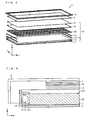
- Figs. 1 and 3 show a light guide 21 having light scatterers 23 formed in a print pattern A.
- a light guide 21A has light scatterers 23A formed in the shape of a print pattern A on that surface of the thick-walled part 21c and fixed parts 21b which faces the chassis 2 (such a surface being hereinafter referred to as "pattern surface 21p").
- pattern surface 21p a surface being hereinafter referred to as "pattern surface 21p"
- the light guide 21 and light scatterers 23 according to the print pattern A are denoted as “light guide 21A” and "light scatterers 23A” to be particularly distinguished from another light guide 21 and other light scatterers 23.
- the light guide 21A has its longer sides each having a length of 1358.5 mm, its shorter sides each having a length of 17 mm, its thick-walled part 21c, i.e. central part, having a thickness of 5 mm, and its fixed parts 21b, i.e. side-edge parts, each having a thickness of 1 mm and a length of 2.5 mm. It should be noted that in the print pattern A, it is preferable that the light guide 21A have its shorter sides each having a length of 15 to 16 mm.
- the print pattern A is a laddery pattern of light scatterers 23A formed on the pattern surface 21p of the light guide 21A, and is symmetrical about the center of the thick-walled part 21c. As evidenced by Fig. 3 , the print pattern A is wide in pattern width in those regions of the pattern surface 21p which face in the opposite direction from those regions (parallel portions) of the emission surface 21d which are parallel to the diffusing plate 15, and is narrow in pattern width in those regions of the pattern surface 21p which face in the opposite direction from those regions (inclined portions, whose angle may be vertical) of the emission surface 2 1 d which are not parallel to the diffusing plate 15.
- each of the light scatterers 23A vary smoothly in pattern width, the light scatterers 23A becomes narrower, starting from that region of the pattern surface 21p which faces in the opposite direction from an edge of such a parallel portion in connection with such an inclined portion.
- each light scatterer 23A has a pattern width of 100 ⁇ m to 500 ⁇ m, for example.
- the luminance is attenuated with an increase in distance from the LEDs 12, i.e. the light sources, it is necessary to make the density of arrangement of the light scatterers 23A higher with an increase in distance from the LEDs 12.
- each light scatterer 23A may be made wider with an increase in distance from an end of the light guide 21A toward its center along its length.
- the light scatterers 23A may be placed at shorter pattern intervals with an increase in distance from an end of the light guide 21A toward its center along its length.
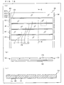
- Fig. 7 which shows a case where light from the LEDs 12 enters through both end surfaces 21a, those light scatterers 23A in the central part of the light guide plate 20 are wide in pattern width.
- Fig. 8 schematically shows an optical path as seen in a cross-section of the light guide 21 along the lateral direction.
- Fig. 8 schematically shows an optical path as seen in a cross-section of the light guide 21 along the lateral direction.
- a print pattern of light scatterers 23 can be determined by obtaining correlation data indicating which part is illuminated when a pattern is placed in a particular part of the pattern surface 21p and by finding a correlation between a distribution of print patterns and a luminance distribution.
- the use of the print pattern A (see Figs. 1 and 3 ) to decrease the pattern width of each light scatterer 23A in those regions of the pattern surface 21p which face in the opposite direction from the inclined portions of the light guide 21A makes it possible to suppress emission of light from the inclined portions, thus preventing the occurrence of luminance unevenness.
- the density of the pattern is adjusted along the lateral direction (or normally, is decreased in those regions facing in the opposite direction from the inclined portions) by varying the pattern width of each light scatterer 23A in those regions facing in the opposite direction from the inclined portions of the light guide 21A, whereby a uniform luminance distribution is achieved.
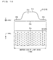
- a second example of a pattern (print pattern B) of light scatterers 23 to be formed on a light guide 21 is described with reference to Fig. 10 .
- Fig. 10 shows a light guide 21 having light scatterers 23 formed in a print pattern B.
- a light guide 21B has light scatterers 23B formed in the shape of a print pattern B on that surface of the thick-walled part 21c and fixed parts 21b which faces the chassis 2 (such a surface being hereinafter referred to as "pattern surface 21p").
- pattern surface 21p a surface being hereinafter referred to as "pattern surface 21p"
- the light guide 21 and light scatterers 23 according to the print pattern B are denoted as “light guide 21B” and “light scatterers 23B” to be particularly distinguished from another light guide 21 and other light scatterers 23.
- the light guide 21B has its longer sides each having a length of 1358.5 mm, its shorter sides each having a length of 17 mm, its thick-walled part 21c, i.e. central part, having a thickness of 5 mm, and its fixed parts 21b, i.e. side-edge parts, each having a thickness of 1 mm and a length of 2.5 mm. It should be noted that in the print pattern B, it is preferable that the light guide 21B have its shorter sides each having a length of 15 to 16 mm.
- the print pattern B is a polka-dot pattern of circular light scatterers 23B formed on the pattern surface 21p of the light guide 21B, and is symmetrical about the center of the thick-walled part 21c. As evidenced by Fig. 10 , the print pattern B is large in dot diameter in those regions of the pattern surface 21p which face in the opposite direction from those regions (parallel portions) of the emission surface 21d which are parallel to the diffusing plate 15, and is small in dot diameter in those regions of the pattern surface 21p which face in the opposite direction from those regions (inclined portions, whose angle may be vertical) of the emission surface 21d which are not parallel to the diffusing plate 15.
- each light scatterer 23B has a dot diameter of 100 ⁇ m to 500 ⁇ m, for example.
- the luminance is attenuated with an increase in distance from the LEDs 12, i.e. the light sources, it is necessary to make the density of arrangement of the light scatterers 23B higher with an increase in distance from the LEDs 12.
- the light scatterers 23B may become larger in dot diameter with an increase in distance from an end of the light guide 21B toward its center along its length.
- the light scatterers 23B may be placed at shorter dot intervals with an increase in distance from an end of the light guide 21B toward its center along its length.
- Fig. 7 which shows a case where light from the LEDs 12 enters through both end surfaces 21a, those light scatterers 23B in the central part of the light guide plate 20 are large in dot diameter.
- Fig. 7 shows a distribution of light scatterers 23B along the lateral direction as being uniform.
- the use of the print pattern B (see Fig. 10 ) to decrease the dot diameter of each light scatterer 23B in those regions of the pattern surface 21p which face in the opposite direction from the inclined portions of the light guide 21B makes it possible to suppress emission of light from the inclined portions, thus preventing the occurrence of luminance unevenness at a joint between light guides 21B.
- the density of the pattern is adjusted along the lateral direction (or normally, is decreased in those regions facing in the opposite direction from the inclined portions) by varying the dot diameter of the light scatterers 23B and/or the dot intervals between the light scatterers 23B in those regions facing in the opposite direction from the inclined portions of the light guide 21B, whereby a uniform luminance distribution is achieved.
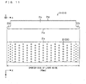
- a third example of a pattern (print pattern C) of light scatterers 23 to be formed on a light guide 21 is described with reference to Fig. 11 .
- Fig. 11 shows a light guide 21 having light scatterers 23 formed in a print pattern C.
- a light guide 21C has light scatterers 23C formed in the shape of a print pattern C on that surface of the thick-walled part 21c and fixed parts 21b which faces the chassis 2 (such a surface being hereinafter referred to as "pattern surface 21p").
- pattern surface 21p a surface being hereinafter referred to as "pattern surface 21p"
- the light guide 21 and light scatterers 23 according to the print pattern C are denoted as “light guide 21C” and “light scatterers 23C” to be particularly distinguished from another light guide 21 and other light scatterers 23.
- the light guide 21C has its longer sides each having a length of 1358.5 mm (possibly varying from 900 to 1600 mm, depending on the screen size), its shorter sides each having a length of 40 mm to 80 mm (possibly having a length 40 mm to 100 mm or greater), its thick-walled part 21c, i.e. central part, having a thickness of 4 mm, and its fixed parts 21b, i.e. side-edge parts, each having a thickness of 1 mm and a length of 2 mm.
- the light guide 21, which has the light scatterers 23 formed in the print pattern C, has grooves 24g formed on the emission surface 21d of the thick-walled part 21c in such a way as to extend along the length of the light guide 21.
- the grooves 24g are placed at pitches of 0.6 mm (or possibly 0.6 mm or greater, e.g. 1 mm) and each have a depth of 0.18 mm (or possibly 0.18 mm or greater, e.g. 0.23 mm, depending on the pitch).
- the light guide 21C has a vertical surface between the thick-walled part 21c and each fixed part 21b and, as such, does not have such an inclined portion as in the case of the print pattern A or B.
- the print pattern C is a polka-dot pattern of circular light scatterers 23C formed on the pattern surface 21p of the light guide 21, and is symmetrical about the center of the thick-walled part 21c. As evidenced by Fig. 11 , the print pattern C is large in dot diameter in those regions of the pattern surface 21p which correspond to the thick-walled part 21c, and is substantially uniform. Further, provided in a position corresponding to a boundary between the thick-walled part 21c and each fixed part 21b is a column of large-diameter dots. Moreover, provided on either side of the column are columns of small-diameter dots.
- each light scatterer 23C has a dot diameter of 100 ⁇ m to 500 ⁇ m (or possibly 100 ⁇ m to 2000 ⁇ m), for example.
- the light scatterers 23C may become larger in dot diameter with an increase in distance from an end of the light guide 21C toward its center along its length.
- the light scatterers 23C may be placed at shorter dot intervals with an increase in distance from an end of the light guide 21C toward its center along its length.
- the light guide 21C does not have an inclined portion for a smooth change in thickness between the thick-walled part 21c and each fixed part 21b and has grooves 21g formed on the emission surface 21d of the thick-walled part 21c in such a way as to extend along the length of the light guide 21C.
- the density of the pattern is adjusted (or normally, is decreased) by varying the dot diameter of the light scatterers 23C and/or the dot intervals between the light scatterers 23C in the vicinity of a position corresponding to a boundary between the thick-walled part 21c and each fixed potion 21b, whereby a uniform luminance distribution is achieved.
- the light source module 10 of the present embodiment can be configured as follows:
- each of the print patterns A and B shows a case where the light scatterers 23 are provided on that side of the light guide 21 which faces the reflecting sheet 11 (i.e., in those regions of the pattern surface 21p which face in the opposite direction from the inclined portions), the print patterns A and B are not necessarily limited to this.
- the light scatterers 23 may be provided on the emission surface 21 d of the light guide 21 (i.e., in the inclined portions). This brings about the same effect as in the case where the light scatterers 23 are provided on that side of the light guide 21 which faces the reflecting sheet 11.
- the concave and convex surfaces on the emission surface 21d of the light guide 21 make printing difficult. This is why in the present embodiment the light scatterers 23 are formed on the pattern surface 21p.
- each of the light scatterers 23 (in the print pattern A) vary in pattern width and the light scatterers 23 (in the print pattern B) vary in dot diameter prior to a change in angle from the thick-walled part 21c to each fixed part 21b. That is, it is preferable that the range within which the pattern is adjusted (i.e., the range within which there is a decrease in pattern width or dot diameter) be a range including the inclined portions and areas therearound.
- the print pattern B shows an example of arrangement of circular dots
- the dots can be in various shapes such as an elliptical shape, a rectangular shape, etc.
- the light guide 21C has grooves 21g formed on the emission surface 21d of the thick-walled part 21c. These grooves 21g function to make it easy to break the total reflection conditions for light guided inside of the light guide 21 and take the light out of the light guide 21. Therefore, the shape of each light scatterer 23 is not limited to the shape of a dot, and may be the shape of such a strip as in the print pattern A. Further, the formation of the grooves 21g allows the light guide 21 to have a greater width.
- each of the fixed parts 21b be in such a shape that that surface of the fixed part 21b which faces the chassis is flush with that surface of the thick-walled part 21c which faces the chassis, because when each of the fixed parts 21b be in such a shape, the surface where the light guide 21 and the chassis 2 touch each other becomes wider.
- the fixed parts 21b are not limited to this. That is, each of the fixed parts 21b may be in any position so long as the light guide 21 can be fixed to the chassis 2. For example, each of the fixed parts 21b may be in a position closer to the emission surface 21d.
- the liquid crystal display apparatus 1 which is an electronic apparatus of the present embodiment, includes a light source module 10 of the present embodiment. This makes it possible to provide a liquid crystal display apparatus 1 including a light source module 10 capable of reducing the occurrence of luminance unevenness.
- a light source module 10 is a light source module 10 including: a plurality of light guides 21 provided in parallel with each other along their length; a plurality of LEDs (light sources) 12 for causing light to enter through at least one end surface 21a of each of the light guides 21 perpendicular to the length of the light guide 21; a plurality of light scatterers (optical path changing sections) 23, provided on that side (emission surface 21d) of each of the light guides 21 through which light exits or that opposite side (pattern surface 21p) of each of the light guides which faces a reflecting sheet 11, which serve to take out light guided inside of the light guides 21; and a chassis 2 on which the light guides 21 are mounted, each of the light guides 21 having a fixed part 21b, formed at at least one side edge of a cross-section of the light guide 21 orthogonal to the length of the light guide 21, with which the light guide 21 is fixed to the chassis 2, the fixed part 21b being thinner than the other side edge of the cross-section of the light guide
- the provision of the thin-walled fixed part 21b at the side edge of the thick-walled part 21c makes it possible to stably fix the light guide 21 to the chassis 2 via the fixed part 21b. This eliminates such problems as occurrence of luminance unevenness due to a shift in position of the light guide 21, breakage due to contact of the light guide 21 with a liquid crystal panel or the like, etc.
- the optical characteristic in the cross-section of the light guide 21 orthogonal to the length of the light guide 21 is influenced by the provision of the thin-walled fixed part 21b, this influence can be compensated for by providing the light scatterers (optical path changing sections) 23 whose density of arrangement in the cross-section has been adjusted. As a result, there appears no bright line or no dark line at a joint between light guides 21; therefore, there occurs no luminance unevenness.
- the light source module 10 is configured such that: the thick-walled part 21c of the light guide 21 (21A) has a chamfered corner at a boundary between the thick-walled part 21c and the fixed part 21b; and the light scatterers (optical path changing sections) 23 (23A) are provided in such strips as to extend along the direction orthogonal to the length of the light guide 21 (21A) and each of the strips has a smaller width in (i) the region where the light guide 21 (21A) varies in thickness between the thick-walled part 21c and the fixed part 21b than in (ii) the other regions, the region (i) including a region where the chamfered corner is provided.
- each of the light scatterers 23A has a smaller pattern width (strip width) in the region (inclined portion or a surface facing in the opposite direction from the inclined portion) where the light guide 21A varies in thickness between the thick-walled part 21c and the fixed part 21b.
- the density of the pattern along the direction (lateral direction) orthogonal to the length of the light guide 21A is easily adjusted by varying the pattern width (strip width) of each of the light scatterers 23A, whereby a uniform luminance distribution can be achieved.
- the light source module 10 is configured such that: the thick-walled part 21c of the light guide 21 (21B) has a chamfered corner at a boundary between the thick-walled part 21c and the fixed part 21b; and the light scatterers (optical path changing sections) 23 (23B) are provided in circles and each of those circles in (i) the region where the light guide 21 (21B) varies in thickness between the thick-walled part 21c and the fixed part 21b has a smaller diameter than each of those circles in (ii) the other regions, the region (i) including a region where the chamfered corner is provided.
- each of those light scatterers 23B in the region (inclined portion or a surface facing in the opposite direction from the inclined portion) where the light guide 21B varies in thickness between the thick-walled part 21c and the fixed part 21b has a smaller circle diameter (dot diameter).
- the density of the pattern along the direction (lateral direction) orthogonal to the length of the light guide 21B is easily adjusted by varying the circle diameter (dot diameter) of the light scatterers 23B, whereby a uniform luminance distribution can be achieved.
- the light source module according to the present invention is configured such that: the light scatterers (optical path changing sections) 23 (23C) are provided on that side of the light guide 21 (21C) which faces the reflecting sheet 11; and the light guide 21 (21C) has grooves 21g formed on that surface (emission surface 21d) of the thick-walled part 21c through which light exits and extending along the length of the light guide 21 (21C).
- the grooves 21g on the surface (emission surface 21d) through which light exits, as well as the light scatterers (optical path changing sections) 23 on the side facing the reflecting sheet 11, function to make it easy to break the total reflection conditions for light guided inside of the light guide 21 and take the light out of the light guide 21.
- a liquid crystal display apparatus (electronic apparatus) 1 of the present embodiment includes a light source module 10 of the present embodiment. This makes it possible to provide an liquid crystal display apparatus including a light source module 10 that allows a light guide to be stably fixed, causes no bright line or no dark line at a joint between light guides, and can achieve a reduction in luminance unevenness.
- FIG. 15 shows that when the thick-walled part 321c has a rectangular shape, part of the beams of light striking a side surface of the thick-walled part 321c is totally reflected; therefore, no beam of light can be taken out from the edge portions. It is obvious that this results in dark lines at the edge portions of the rectangular thick-walled part 321c.
- (c) of Fig. 15 shows that when the light guide 321 has such a curved shape that its thick-walled part 321c has chamfered top corners, those beams of light emitted from the central part of the lower surface of the thick-walled part 321c of the light guide 321 and having entered the chamfered curved shapes have been gathered. This may result in bright lines at the chamfered portions of the rectangular thick-walled part 321c.
- Fig. 16 is a graph showing a relationship between the position and luminance of a light source module including light guides 321 each having such a curved shape that its thick-walled part 321c has chamfered top corners. It should be noted that the light guide 321 has light scatterers 323 uniformly formed in a print pattern along the lateral direction on that surface of the light guide 321 which faces the reflecting sheet.
- Fig. 16 shows that in a light source module including light guides 321 each having such a curved shape that its thick-walled part 321c has chamfered top corners and each having rectangular light scatterers 323 formed in a laddery print pattern, there appears a bright line at the joint between the light guides 321.
- a light source module is a light source module including: a plurality of light guides provided in parallel with each other along their length; a plurality of light sources for causing light to enter through at least one end surface of each of the light guides perpendicular to the length of the light guide; a plurality of optical path changing sections, provided on that side of each of the light guides through which light exits or that opposite side of each of the light guides which faces a reflecting sheet, which serve to take out light guided inside of the light guides; and a chassis on which the light guides are mounted, each of the light guides having a fixed part, formed at at least one side edge of a cross-section of the light guide orthogonal to the length of the light guide, with which the light guide is fixed to the chassis, the fixed part being thinner than the other side edge of the cross-section of the light guide orthogonal to the length of the light guide or a thick-walled part that is a central part of the cross-section of the light guide orthogonal to the length of the light guide
- the provision of the thin-walled fixed part at the side edge of the thick-walled part makes it possible to stably fix the light guide to the chassis via the fixed part. This eliminates such problems as occurrence of luminance unevenness due to a shift in position of the light guide, breakage due to contact of the light guide with a liquid crystal panel or the like, etc.
- the optical characteristic in the cross-section of the light guide orthogonal to the length of the light guide is influenced by the provision of the thin-walled fixed part, this influence can be compensated for by providing the optical path changing sections whose density of arrangement in the cross-section has been adjusted. As a result, there appears no bright line or no dark line at a joint between light guides; therefore, there occurs no luminance unevenness.
- the light source module according to the present invention is configured such that: the thick-walled part of the light guide has a chamfered corner at a boundary between the thick-walled part and the fixed part; and the optical path changing sections are provided in such strips as to extend along the direction orthogonal to the length of the light guide and each of the strips has a smaller width in (i) the region where the light guide varies in thickness between the thick-walled part and the fixed part than in (ii) the other regions, the region (i) including a region where the chamfered corner is provided.
- each of the optical path changing sections has a smaller pattern width (strip width) in the region (inclined portion or a surface facing in the opposite direction from the inclined portion) where the light guide varies in thickness between the thick-walled part and the fixed part.
- the density of the pattern along the direction (lateral direction) orthogonal to the length of the light guide is easily adjusted by varying the pattern width (strip width) of each of the optical path changing sections, whereby a uniform luminance distribution can be achieved.
- the light source module according to the present invention is configured such that: the thick-walled part of the light guide has a chamfered corner at a boundary between the thick-walled part and the fixed part; and the optical path changing sections are provided in circles and each of those circles in (i) the region where the light guide varies in thickness between the thick-walled part and the fixed part has a smaller diameter than each of those circles in (ii) the other regions, the region (i) including a region where the chamfered corner is provided.
- each of those optical path changing sections in the region (inclined portion or a surface facing in the opposite direction from the inclined portion) where the light guide varies in thickness between the thick-walled part and the fixed part has a smaller circle diameter (dot diameter).
- the density of the pattern along the direction (lateral direction) orthogonal to the length of the light guide is easily adjusted by varying the circle diameter (dot diameter) of the optical path changing sections, whereby a uniform luminance distribution can be achieved.
- the light source module according to the present invention is configured such that: the optical path changing sections are provided on that side of the light guide which faces the reflecting sheet; and the light guide has grooves formed on that surface of the thick-walled part through which light exits and extending along the length of the light guide.
- the grooves on the surface through which light exits, as well as the optical path changing sections on the side facing the reflecting sheet, function to make it easy to break the total reflection conditions for light guided inside of the light guide and take the light out of the light guide. This makes it easier to achieve a uniform luminance distribution in comparison with the case where only the optical path changing sections are provided. This makes it possible to realize a light guide that is greater in width along the direction (lateral direction) orthogonal to its length.
- the present invention relates to: a light source module including a side-edge (referred to also as "side-light") light guide plate through which light from a light source is emitted in planar form; and an electronic apparatus including such a light source module.
- a light source module including a side-edge (referred to also as "side-light") light guide plate through which light from a light source is emitted in planar form; and an electronic apparatus including such a light source module.
- the present invention can be applied to a light source module such as a backlight and an electronic apparatus such as a liquid crystal display apparatus.
Landscapes
- Physics & Mathematics (AREA)
- General Physics & Mathematics (AREA)
- Optics & Photonics (AREA)
- Engineering & Computer Science (AREA)
- Microelectronics & Electronic Packaging (AREA)
- Instantaneous Water Boilers, Portable Hot-Water Supply Apparatuses, And Control Of Portable Hot-Water Supply Apparatuses (AREA)
- Details Of Fluid Heaters (AREA)
- Heat-Exchange Devices With Radiators And Conduit Assemblies (AREA)
- Planar Illumination Modules (AREA)
Abstract
Each light guide (21) has a fixed part (21b), formed at at least one side edge of a cross-section of the light guide (21) orthogonal to the length of the light guide (21), with which the light guide (21) is fixed to a chassis. The fixed part (21b) is thinner than the other side edge of the cross-section of the light guide (21) orthogonal to the length of the light guide (21) or a thick-walled part (21c) that is a central part of the cross-section of the light guide (21) orthogonal to the length of the light guide (21). Light scatterers (23) vary in density of arrangement between (i) a region where the light guide (21) varies in thickness between the thick-walled part (21c) and the fixed part (21b) and (ii) other regions along a direction orthogonal to the length of the light guide (21). Thus, the light guide (21) can be fixed via the fixed part (21b), and the influence on the optical characteristic by the provision of the thin-walled fixed part (21b) can be compensated for by providing the light scatterers (23) whose density of arrangement along the lateral direction has been adjusted.
Description
- The present invention relates to: a light source module which, for the purpose of achieving a reduction in thickness, for example, of a liquid crystal display apparatus, is used as a backlight including a side-edge (referred to also as "side-light") light guide plate through which light from light sources is emitted in planar form; and an electronic apparatus including such a light source module.
- In recent years, for the purpose of achieving a reduction in thickness of liquid crystal display apparatuses, backlights has been in heavy usage each of which includes a side-edge type (referred to also as "side-light type") light guide plate through which light from light sources is emitted in planar form.
- Such a side-edge type light guide plate is included, for example, in an illumination device disclosed in
Patent Literature 1.Fig. 12 schematically shows the configuration of the illumination device disclosed in -
Patent Literature 1. Theillumination device 100 disclosed inPatent Literature 1 includes: alight guide plate 110 composed of a plurality oflight guides 111 arranged in a line; and a plurality oflight sources 101, provided for each separate one of thelight guides 111 of thelight guide plate 110, which irradiate thelight guides 111 with light. Thelight sources 101 are each composed of one red LED (light-emitting diode) 101R, twogreen LEDs 101G, and oneblue LED 101B (see (a) ofFig. 12 ). Further, thelight guide plate 110 has a reflectingsheet 102 provided therebelow (see (b) ofFig. 12 ). Moreover, each of thelight guides 111 is separated from itsadjacent light guide 111 by agap 103 composed of an air layer of 0.1 µm or greater (see (c) ofFig. 12 ). This configuration makes it possible to carry out a pseudo impulse-type display. - Further, for example,
Patent Literature 2 discloses a light emitter structure of the same kind. Furthermore,Patent Literature 2 discloses a structure in which reflecting dots for changing the direction of light are provided in a print pattern with a variation in density of the reflecting dots along the length of an elongated light emitter (seeFig. 13 ). As shown inFig. 13 , the density of the reflectingdots 201 varies from alight input end 215 and from amixing section 281 to the center of the elongated light emitter. Further, in order to attain uniform light extraction and illumination from one end of the light emitter to the other end,Patent Literature 2 discloses varying the reflectingdots 201 in size and shape as a function of distance from themixing section 281, as well as from thelight input end 215. -
-
Patent Literature 1 - Japanese Patent Application Publication, Tokukai, No.
2008-34372 A (Publication Date: February 14, 2008 -
Patent Literature 2 - Japanese Patent Application Publication, Tokukai, No.
2009-43706 A (Publication Date: February 28, 2009 - In the conventional configuration, as shown in
Fig. 14 ,light guides 111 each having a rectangular cross-section have been fixedly sandwiched between achassis 2 and adiffusing plate 15. However, because thediffusing plate 15 is weak in strength, the fixation of thelight guides 111 has been insufficient. Therefore, there have been such problems as occurrence of luminance unevenness due to a shift in position of thelight guides 111, breakage due to contact of thelight guides 111 with a liquid crystal panel or the like, etc. - These problems can possibly be solved by providing
light guides 21 each having a such a T-shaped cross-section as to have a thick-walled part 21c in the center and thin-walled fixedparts 21b at both ends of the thick-walled part 2 1 c and, for example, by interposing thefixed parts 21b and thechassis 2 together betweenupper holding members 52 and alower holding member 51 of afixing piece 50, as shown inFig. 2 , which is an explanatory diagram of the present invention. - However, because the thin-walled fixed
parts 21b differ in optical characteristic from the thick-walled part 21c, the mere provision of the fixedparts 21b for fixation results in a bright line or a dark line at a joint between light guides, thus making it difficult to achieve uniform luminance. - The present invention has been made in view of the foregoing conventional problems, and it is an object of the present invention to provide: a light source module which has light guides each provided with a fixed part and which reduces the occurrence of luminance unevenness at a joint between light guides; and an electronic apparatus including such a light source module.
- In order to solve the foregoing problems, a light source module according to the present invention is a light source module including: a plurality of light guides provided in parallel with each other along their length; a plurality of light sources for causing light to enter through at least one end surface of each of the light guides perpendicular to the length of the light guide; a plurality of optical path changing sections, provided on that side of each of the light guides through which light exits or that opposite side of each of the light guides which faces a reflecting sheet, which serve to take out light guided inside of the light guides; and a chassis on which the light guides are mounted, each of the light guides having a fixed part, formed at at least one side edge of a cross-section of the light guide orthogonal to the length of the light guide, with which the light guide is fixed to the chassis, the fixed part being thinner than the other side edge of the cross-section of the light guide orthogonal to the length of the light guide or a thick-walled part that is a central part of the cross-section of the light guide orthogonal to the length of the light guide, the optical path changing sections varying in density of arrangement between (i) a region where the light guide varies in thickness between the thick-walled part and the fixed part and (ii) other regions along a direction orthogonal to the length of the light guide.
- According to the foregoing configuration, the provision of the thin-walled fixed part at the side edge of the thick-walled part makes it possible to stably fix the light guide to the chassis via the fixed part. This eliminates such problems as occurrence of luminance unevenness due to a shift in position of the light guide, breakage due to contact of the light guide with a liquid crystal panel or the like, etc.
- Further, although the optical characteristic in the cross-section of the light guide orthogonal to the length of the light guide is influenced by the provision of the thin-walled fixed part, this influence can be compensated for by providing the optical path changing sections whose density of arrangement in the cross-section has been adjusted. As a result, there appears no bright line or no dark line at a joint between light guides; therefore, there occurs no luminance unevenness.
- This makes it possible to provide a light source module that allows a light guide to be stably fixed and imparts uniform luminance to a display.
- Further, an electronic apparatus according to the present invention includes such a light source module as described above.
- The foregoing configuration brings about an effect of making it possible to provide an electronic apparatus including a light source module that allows a light guide to be stably fixed, causes no bright line or no dark line at a joint between light guides, and can achieve a reduction in luminance unevenness.
- A light source module according to the present invention is configured such that: each of the light guides has a fixed part, formed at at least one side edge of a cross-section of the light guide orthogonal to the length of the light guide, with which the light guide is fixed to the chassis, the fixed part being thinner than the other side edge of the cross-section of the light guide orthogonal to the length of the light guide or a thick-walled part that is a central part of the cross-section of the light guide orthogonal to the length of the light guide; and, the optical path changing sections vary in density of arrangement between (i) a region where the light guide varies in thickness between the thick-walled part and the fixed part and (ii) other regions along a direction orthogonal to the length of the light guide.
- Further, an electronic apparatus according to the present invention includes such a light source module as described above.
- This brings about an effect of making it possible to provide: a light source module that allows a light guide to be stably fixed and imparts uniform luminance to a display; and an electronic apparatus including such a light source module.
- Additional objects, features, and strengths of the present invention will be made clear by the description below. Further, the advantages of the present invention will be evident from the following explanation in reference to the drawings.
-
-
Fig. 1
Fig. 1 is a perspective view showing an example of the structure of a light guide constituting a light guide plate in accordance with an embodiment of a light source module of the present invention. -
Fig. 2
Fig. 2 is a cross-sectional view showing a structure for mounting of light guides in the light source module. -
Fig. 3
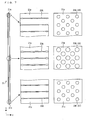
Fig. 3 is a front view and a plan view both showing an example of the structure of the light guide shown inFig. 1 . -
Fig. 4
Fig. 4 is an exploded perspective view showing the configuration of a liquid crystal display apparatus including the light source module. -
Fig. 5
Fig. 5 is a cross-sectional view showing the configuration of a relevant part of the liquid crystal display apparatus including the light source module. -
Fig. 6
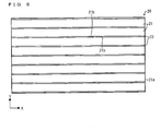
Fig. 6 is a plan view showing the configuration of light guide plates in the light source module. -
Fig. 7
Fig. 7 is an explanatory diagram schematically showing the structures of such light guides as shown inFigs. 1 and10 . -
Fig. 8
Fig. 8 explains how to determine a print pattern of light scatterers to be formed on the light guide shown inFig. 1 , and shows an optical path as seen in a cross-section of the light guide along the lateral direction. -
Fig. 9
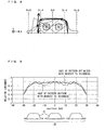
Fig. 9 is an explanatory diagram showing a state of luminance uniformed by a light source module including such light guides as shown inFig. 1 . -
Fig. 10
Fig. 10 is a front view and a plan view both showing another example of the structure of a light guide constituting a light guide plate in accordance with an embodiment of a light source module of the present invention. -
Fig. 11
Fig. 11 is a front view and a plan view both showing still another example of the structure of a light guide constituting a light guide plate in accordance with an embodiment of a light source module of the present invention. -
Fig. 12
Fig. 12 includes: (a) a plan view showing the configuration of a conventional light source module; (b) a front view showing the configuration of the light source module; and (c) a cross-sectional view taken along the line A-A' of (a). -
Fig. 13
Fig. 13 is a plan view showing the configuration of a conventional light source module. -
Fig. 14
Fig. 14 is a cross-sectional view showing a structure for mounting of light guides in a conventional light source module. -
Fig. 15
Fig. 15 , showing a background of the present invention, includes: (a) a cross-sectional view of a light guide showing a position of emission of light from light sources in the case of an experiment for comparing (i) a light guide having a rectangular cross-section and (ii) a light guide having such a curved cross-section as to have chamfered top corners, concerning an optical path along which light from light sources is emitted through a light guide; (b) a cross-sectional view of a light guide showing an optical path in a light guide having such a rectangular cross-section as to have non-chamfered top corners; and (c) a cross-sectional view of a light guide showing an optical path in a light guide having such a curved cross-section as to have chamfered top corners. -
Fig. 16
Fig. 16 , showing a background of the present invention, is a graph showing a relationship between the position and luminance of a light source module including light guides each having such a curved shape that its thick-walled part has chamfered top corners. - The present invention is described below more in detail by way of Examples and Comparative Examples; however, the present invention is in no way limited to these examples.
- An embodiment of the present invention is described below with reference to
Figs. 1 through 11 . - First, the configuration of a liquid
crystal display apparatus 1 that is an example of an electronic apparatus including alight source module 10 of the present embodiment is described below with reference toFigs. 4 through 6 . - As shown in
Fig. 4 , the liquidcrystal display apparatus 1 is constituted by achassis 2, alight source module 10, aliquid crystal panel 3, and abezel 4, starting from the bottom. Thelight source module 10 is constituted by: a reflectingsheet 11, which serves as a reflecting plate; LEDs (light-emitting diodes) 12, which serve as light sources, andLED substrates 13;reflectors 14; anlight guide plate 20, a diffusingplate 15; and anoptical sheet group 16, starting from the bottom. It should be noted that theoptical sheet group 16 does not need to be present in the present invention. - As shown in
Fig. 5 , theLEDs 12, theLED substrates 13, and thereflectors 14 are provided at both ends of thelight guide plate 20, whereby light from theLEDs 12 enters through oneend surface 21a of thelight guide plate 20 and theliquid crystal panel 3 is irradiated with light from anemission surface 21d of thelight guide plate 20 through the diffusingplate 15 and theoptical sheet group 16. Therefore, thelight source module 10 of the present embodiment employs a side-edge (also referred to as "side-light") method. - In the present embodiment, the diffusing
plate 15 is provided above anemission surface 21d of alight guide 21 with a distance D, for example, of 2 mm therebetween. This makes it possible to make luminance unevenness less than in a case where the diffusingplate 15 is in close contact with theemission surface 21d of thelight guide 21. - Unlike a CRT (cathode-ray tube) display apparatus, the liquid
crystal display apparatus 1 suffers from blurring of a moving image. That is, the CRT display device gives little sense of afterimage, because between a light-emitting period of a pixel in one frame and a light-emitting period of the pixel in the next frame, there is a non-light-emitting period during which the pixel does not emit light. On the other hand, the liquidcrystal display apparatus 1 employs a "hold-type" display method without such a non-light-emitting period and therefore gives a sense of afterimage, and this sense of afterimage is perceived by users as blurring of a moving image. - Proposed in view of this for the backlight-type liquid
crystal display apparatus 1 is a backlight blinking technique for inserting a black display between one image display and another by dividing thelight source module 10, which is a backlight, into parts and by turning off these parts in sequence in synchronization with the timing of application of video signals to theliquid crystal panel 3. This makes it possible to realize a pseudo impulse-type display and suppress a sense of afterimage. - In order to carry out the backlight blinking, the
light source module 10 of the present embodiment is constituted by dividing thelight guide plate 20 into a plurality of light guides 21 and disposing these light guides 21 in parallel with each other along their length withgaps 22 therebetween, as shown inFig. 6 . Therefore, in the present embodiment, as shown inFig. 5 , theLEDs 12 cause light to enter the after-mentioned thick-walled part 21c (seeFig. 2 ) through oneend surface 21a of each of the light guides 21 perpendicular to the length of thelight guide 21. It should be noted that the light may enter through the other end surface of thelight guide 21 perpendicular to the length of thelight guide 21, instead of entering through the oneend surface 21a. Alternatively, the light may enter through both the one end surface and the other end surface. That is, in the present invention, the light only needs to enter through at least the oneend surface 21a. - In consideration of thermal expansion and manufacturing tolerance of the light guides 21, it is necessary to dispose the light guides 21, into which the
light guide plate 20 has been divided, so that they are parallel to each other along their length withgaps 22 of approximately 1 to 2 mm therebetween. - Next, a structure for mounting of the light guides 21 in the
light source module 10 is described with reference toFig. 2 . - As shown in
Fig. 2 , each of the light guides 21, into which thelight guide plate 20 has been divided, has such a T-shaped cross-section as to have a thick-walled part 21c in the center and thin-walledfixed parts 21b at both ends of the thick-walled part 21c. That is, each of the fixedparts 21b is in such a shape that that surface of thefixed part 21b which faces thechassis 2 is flush with that surface of the thick-walled part 21c which faces thechassis 2. Moreover, thelight guide plate 20 is fixed to thechassis 2 by interposing the fixedparts 21b and thechassis 2 together between upper holdingmembers 52 and alower holding member 51 of a fixingpiece 50. - This makes it possible to stably fix the plurality of light guides 21 to the
chassis 2, thus preventing the occurrence of luminance unevenness due to a shift in position, breakage due to contact with a liquid crystal panel or the like, etc., as has been done conventionally. - Furthermore, the detailed shape of each of the light guides 21 is as follows: Each of the fixed
parts 21b, which serve as side-edge parts across which thelight guide 21 faces its adjacentlight guide 21, is thinner than the thick-walled part 21c, which serves as the central part of a cross-section of thelight guide 21 orthogonal to the length of thelight guide 21. As a result, each of the light guides 21 of the present embodiment has such a T-shaped cross-section as to haveabsent parts 21f at its side-edge parts toward the reflectingsheet 11 and, as such, is composed of a thick-walled part 21c formed thick andfixed parts 21b formed thin. - It should be noted that the structure of the fixing
piece 50 is not limited to that shown inFig. 2 and it is possible to select a fixingpiece 50 of any structure that allows the fixedparts 21b to be mounted directly or indirectly to thechassis 2. - The following describes a configuration for preventing luminance unevenness from occurring at a joint between light guides 21 due to the provision of the fixed
parts 21b. - Light traveling through a
light guide 21 exits thelight guide 21 through anemission surface 2 1 d when the total reflection conditions are broken by a change in angle at which the light travels through thelight guide 21 due to collision of the light withlight scatterers 23 serving as optical path changing sections, and then travels toward the diffusingplate 15. Therefore, a luminance distribution of emitted light can be controlled by determining where on thelight guide 21 and how densely thelight scatterers 23 are arranged. - The following describes a print pattern of
light scatterers 23 for compensating for a change in optical characteristic as caused by providing the thin-walledfixed parts 21b. - In the present embodiment, the
light scatterers 23 are formed, for example, by printing light-scattering microparticles dispersed in a polymer; however, thelight scatterers 23 are not necessarily limited to this, and may be formed by another method. For example, the light-scattering particles may be a fluorescent substance. Alternatively, thelight scatterers 23 may be formed by forming minute concave-convex shapes such as prisms. Alternatively, it is also possible to form a pattern by providing a rough surface as an emission surface or reflecting-sheet-facing surface by blasting or the like. - A first example of a pattern (print pattern A) of
light scatterers 23 to be formed on alight guide 21 is described with reference toFigs. 1 ,3 , and7 through 9 . -
Figs. 1 and3 show alight guide 21 havinglight scatterers 23 formed in a print pattern A. As shown inFigs. 1 and3 , alight guide 21A haslight scatterers 23A formed in the shape of a print pattern A on that surface of the thick-walled part 21c and fixedparts 21b which faces the chassis 2 (such a surface being hereinafter referred to as "pattern surface 21p"). It should be noted that thelight guide 21 andlight scatterers 23 according to the print pattern A are denoted as "light guide 21A" and "light scatterers 23A" to be particularly distinguished from anotherlight guide 21 andother light scatterers 23. - For example, the
light guide 21A has its longer sides each having a length of 1358.5 mm, its shorter sides each having a length of 17 mm, its thick-walled part 21c, i.e. central part, having a thickness of 5 mm, and itsfixed parts 21b, i.e. side-edge parts, each having a thickness of 1 mm and a length of 2.5 mm. It should be noted that in the print pattern A, it is preferable that thelight guide 21A have its shorter sides each having a length of 15 to 16 mm. - The print pattern A is a laddery pattern of
light scatterers 23A formed on thepattern surface 21p of thelight guide 21A, and is symmetrical about the center of the thick-walled part 21c. As evidenced byFig. 3 , the print pattern A is wide in pattern width in those regions of thepattern surface 21p which face in the opposite direction from those regions (parallel portions) of theemission surface 21d which are parallel to the diffusingplate 15, and is narrow in pattern width in those regions of thepattern surface 21p which face in the opposite direction from those regions (inclined portions, whose angle may be vertical) of theemission surface 2 1 d which are not parallel to the diffusingplate 15. However, because it is preferable that each of thelight scatterers 23A vary smoothly in pattern width, thelight scatterers 23A becomes narrower, starting from that region of thepattern surface 21p which faces in the opposite direction from an edge of such a parallel portion in connection with such an inclined portion. In the present embodiment, eachlight scatterer 23A has a pattern width of 100 µm to 500 µm, for example. - It should be noted here that because the luminance is attenuated with an increase in distance from the
LEDs 12, i.e. the light sources, it is necessary to make the density of arrangement of thelight scatterers 23A higher with an increase in distance from theLEDs 12. - Accordingly, as shown in
Fig. 7 , the pattern width of eachlight scatterer 23A may be made wider with an increase in distance from an end of thelight guide 21A toward its center along its length. Alternatively, thelight scatterers 23A may be placed at shorter pattern intervals with an increase in distance from an end of thelight guide 21A toward its center along its length. InFig. 7 , which shows a case where light from theLEDs 12 enters through bothend surfaces 21a, thoselight scatterers 23A in the central part of thelight guide plate 20 are wide in pattern width. - How to determine a print pattern of
light scatterers 23 is described here with reference toFig. 8 . -
Fig. 8 schematically shows an optical path as seen in a cross-section of thelight guide 21 along the lateral direction. For example, in the case of an arrangement oflight scatterers 23 in the vicinity of X = -4, light reflected by thelight scatterers 23 causes total reflection inside of thelight guide 21 as indicated by arrows in the drawing and exits through the vicinity of X = 4. This shows that light exits through a place other than the place where thelight scatterers 23 are arranged. - Accordingly, by allowing beams of light to enter at positions (X = -8 to 8 in
Fig. 8 ) along the lateral direction and finding where each of the beams of light exits, data on a luminance distribution of light reflected by thelight scatterers 23 in the respective positions can be obtained. Moreover, by analyzing such a pattern shape that the sum of the data constitutes a uniform distribution, the shape of a print pattern having such a thickness distribution as shown inFig. 3 is obtained. - In this way, a print pattern of
light scatterers 23 can be determined by obtaining correlation data indicating which part is illuminated when a pattern is placed in a particular part of thepattern surface 21p and by finding a correlation between a distribution of print patterns and a luminance distribution. - Next, an example of luminance uniformed by forming
light scatterers 23 in a print pattern A in alight source module 10 including threelight guides 21 is described with reference toFig. 9 . - As shown in
Fig. 9 , in the case of an arrangement of light scatterers in a pattern uniform with respect to the section thickness of each light guide, approximately 20% of irregularities in luminance were observed (as indicated by a dotted line). On the other hand, in the case of an arrangement of light scatterers in a pattern whose density has been optimized with respect to the section thickness of each light guide 21 (seeFig. 3 ), an improvement in irregularities in luminance was observed (as indicated by a solid line). - As described above, the use of the print pattern A (see
Figs. 1 and3 ) to decrease the pattern width of eachlight scatterer 23A in those regions of thepattern surface 21p which face in the opposite direction from the inclined portions of thelight guide 21A makes it possible to suppress emission of light from the inclined portions, thus preventing the occurrence of luminance unevenness. - Thus, in the print pattern A, the density of the pattern is adjusted along the lateral direction (or normally, is decreased in those regions facing in the opposite direction from the inclined portions) by varying the pattern width of each
light scatterer 23A in those regions facing in the opposite direction from the inclined portions of thelight guide 21A, whereby a uniform luminance distribution is achieved. - A second example of a pattern (print pattern B) of
light scatterers 23 to be formed on alight guide 21 is described with reference toFig. 10 . -
Fig. 10 shows alight guide 21 havinglight scatterers 23 formed in a print pattern B. As shown inFig. 10 , alight guide 21B haslight scatterers 23B formed in the shape of a print pattern B on that surface of the thick-walled part 21c and fixedparts 21b which faces the chassis 2 (such a surface being hereinafter referred to as "pattern surface 21p"). It should be noted that thelight guide 21 andlight scatterers 23 according to the print pattern B are denoted as "light guide 21B" and "light scatterers 23B" to be particularly distinguished from anotherlight guide 21 andother light scatterers 23. - For example, as in the case of the print pattern A, the
light guide 21B has its longer sides each having a length of 1358.5 mm, its shorter sides each having a length of 17 mm, its thick-walled part 21c, i.e. central part, having a thickness of 5 mm, and itsfixed parts 21b, i.e. side-edge parts, each having a thickness of 1 mm and a length of 2.5 mm. It should be noted that in the print pattern B, it is preferable that thelight guide 21B have its shorter sides each having a length of 15 to 16 mm. - The print pattern B is a polka-dot pattern of
circular light scatterers 23B formed on thepattern surface 21p of thelight guide 21B, and is symmetrical about the center of the thick-walled part 21c. As evidenced byFig. 10 , the print pattern B is large in dot diameter in those regions of thepattern surface 21p which face in the opposite direction from those regions (parallel portions) of theemission surface 21d which are parallel to the diffusingplate 15, and is small in dot diameter in those regions of thepattern surface 21p which face in the opposite direction from those regions (inclined portions, whose angle may be vertical) of theemission surface 21d which are not parallel to the diffusingplate 15. However, because it is preferable that thelight scatterers 23B vary smoothly in dot diameter, thelight scatterers 23B become smaller in dot diameter, starting from that region of thepattern surface 21p which faces in the opposite direction from an edge of such a parallel portion in connection with such an inclined portion. In the present embodiment, eachlight scatterer 23B has a dot diameter of 100 µm to 500 µm, for example. - It should be noted here that because the luminance is attenuated with an increase in distance from the
LEDs 12, i.e. the light sources, it is necessary to make the density of arrangement of thelight scatterers 23B higher with an increase in distance from theLEDs 12. - Accordingly, as shown in
Fig. 7 , thelight scatterers 23B may become larger in dot diameter with an increase in distance from an end of thelight guide 21B toward its center along its length. Alternatively, thelight scatterers 23B may be placed at shorter dot intervals with an increase in distance from an end of thelight guide 21B toward its center along its length. InFig. 7 , which shows a case where light from theLEDs 12 enters through bothend surfaces 21a, thoselight scatterers 23B in the central part of thelight guide plate 20 are large in dot diameter. It should be noted that in order to help show only a distribution oflight scatterers 23B along the length of thelight guide 21B,Fig. 7 shows a distribution oflight scatterers 23B along the lateral direction as being uniform. - As described above, the use of the print pattern B (see
Fig. 10 ) to decrease the dot diameter of eachlight scatterer 23B in those regions of thepattern surface 21p which face in the opposite direction from the inclined portions of thelight guide 21B makes it possible to suppress emission of light from the inclined portions, thus preventing the occurrence of luminance unevenness at a joint between light guides 21B. - Thus, in the print pattern B, the density of the pattern is adjusted along the lateral direction (or normally, is decreased in those regions facing in the opposite direction from the inclined portions) by varying the dot diameter of the
light scatterers 23B and/or the dot intervals between thelight scatterers 23B in those regions facing in the opposite direction from the inclined portions of thelight guide 21B, whereby a uniform luminance distribution is achieved. - A third example of a pattern (print pattern C) of
light scatterers 23 to be formed on alight guide 21 is described with reference toFig. 11 . -
Fig. 11 shows alight guide 21 havinglight scatterers 23 formed in a print pattern C. As shown inFig. 11 , alight guide 21C haslight scatterers 23C formed in the shape of a print pattern C on that surface of the thick-walled part 21c and fixedparts 21b which faces the chassis 2 (such a surface being hereinafter referred to as "pattern surface 21p"). It should be noted that thelight guide 21 andlight scatterers 23 according to the print pattern C are denoted as "light guide 21C" and "light scatterers 23C" to be particularly distinguished from anotherlight guide 21 andother light scatterers 23. - For example, unlike in the case of the print pattern A or B, the
light guide 21C has its longer sides each having a length of 1358.5 mm (possibly varying from 900 to 1600 mm, depending on the screen size), its shorter sides each having a length of 40 mm to 80 mm (possibly having alength 40 mm to 100 mm or greater), its thick-walled part 21c, i.e. central part, having a thickness of 4 mm, and itsfixed parts 21b, i.e. side-edge parts, each having a thickness of 1 mm and a length of 2 mm. Furthermore, thelight guide 21, which has thelight scatterers 23 formed in the print pattern C, has grooves 24g formed on theemission surface 21d of the thick-walled part 21c in such a way as to extend along the length of thelight guide 21. The grooves 24g are placed at pitches of 0.6 mm (or possibly 0.6 mm or greater, e.g. 1 mm) and each have a depth of 0.18 mm (or possibly 0.18 mm or greater, e.g. 0.23 mm, depending on the pitch). Further, thelight guide 21C has a vertical surface between the thick-walled part 21c and eachfixed part 21b and, as such, does not have such an inclined portion as in the case of the print pattern A or B. - The print pattern C is a polka-dot pattern of
circular light scatterers 23C formed on thepattern surface 21p of thelight guide 21, and is symmetrical about the center of the thick-walled part 21c. As evidenced byFig. 11 , the print pattern C is large in dot diameter in those regions of thepattern surface 21p which correspond to the thick-walled part 21c, and is substantially uniform. Further, provided in a position corresponding to a boundary between the thick-walled part 21c and eachfixed part 21b is a column of large-diameter dots. Moreover, provided on either side of the column are columns of small-diameter dots. That is, one of the two columns of small-diameter dots is provided in the thick-walled part 21c, and the other in thefixed part 21b. In the present embodiment, eachlight scatterer 23C has a dot diameter of 100 µm to 500 µm (or possibly 100 µm to 2000 µm), for example. - Also in the print pattern C, as shown in
Fig. 7 , as with the print pattern B, thelight scatterers 23C may become larger in dot diameter with an increase in distance from an end of thelight guide 21C toward its center along its length. Alternatively, thelight scatterers 23C may be placed at shorter dot intervals with an increase in distance from an end of thelight guide 21C toward its center along its length. - Thus, in the print pattern C (see
Fig. 11 ), thelight guide 21C does not have an inclined portion for a smooth change in thickness between the thick-walled part 21c and eachfixed part 21b and hasgrooves 21g formed on theemission surface 21d of the thick-walled part 21c in such a way as to extend along the length of thelight guide 21C. Moreover, the density of the pattern is adjusted (or normally, is decreased) by varying the dot diameter of thelight scatterers 23C and/or the dot intervals between thelight scatterers 23C in the vicinity of a position corresponding to a boundary between the thick-walled part 21c and eachfixed potion 21b, whereby a uniform luminance distribution is achieved. - It should be noted that the
light source module 10 of the present embodiment can be configured as follows: - Although each of the print patterns A and B shows a case where the
light scatterers 23 are provided on that side of thelight guide 21 which faces the reflecting sheet 11 (i.e., in those regions of thepattern surface 21p which face in the opposite direction from the inclined portions), the print patterns A and B are not necessarily limited to this. In each of the print patterns A and B, thelight scatterers 23 may be provided on theemission surface 21 d of the light guide 21 (i.e., in the inclined portions). This brings about the same effect as in the case where thelight scatterers 23 are provided on that side of thelight guide 21 which faces the reflectingsheet 11. However, the concave and convex surfaces on theemission surface 21d of thelight guide 21 make printing difficult. This is why in the present embodiment thelight scatterers 23 are formed on thepattern surface 21p. - It is preferable that each of the light scatterers 23 (in the print pattern A) vary in pattern width and the light scatterers 23 (in the print pattern B) vary in dot diameter prior to a change in angle from the thick-
walled part 21c to eachfixed part 21b. That is, it is preferable that the range within which the pattern is adjusted (i.e., the range within which there is a decrease in pattern width or dot diameter) be a range including the inclined portions and areas therearound. - Although the print pattern B shows an example of arrangement of circular dots, the dots can be in various shapes such as an elliptical shape, a rectangular shape, etc.
- In the print pattern C, the
light guide 21C hasgrooves 21g formed on theemission surface 21d of the thick-walled part 21c. Thesegrooves 21g function to make it easy to break the total reflection conditions for light guided inside of thelight guide 21 and take the light out of thelight guide 21. Therefore, the shape of eachlight scatterer 23 is not limited to the shape of a dot, and may be the shape of such a strip as in the print pattern A. Further, the formation of thegrooves 21g allows thelight guide 21 to have a greater width. - It is preferable that each of the fixed
parts 21b be in such a shape that that surface of thefixed part 21b which faces the chassis is flush with that surface of the thick-walled part 21c which faces the chassis, because when each of the fixedparts 21b be in such a shape, the surface where thelight guide 21 and thechassis 2 touch each other becomes wider. However, the fixedparts 21b are not limited to this. That is, each of the fixedparts 21b may be in any position so long as thelight guide 21 can be fixed to thechassis 2. For example, each of the fixedparts 21b may be in a position closer to theemission surface 21d. - Further, the liquid
crystal display apparatus 1, which is an electronic apparatus of the present embodiment, includes alight source module 10 of the present embodiment. This makes it possible to provide a liquidcrystal display apparatus 1 including alight source module 10 capable of reducing the occurrence of luminance unevenness. - As described above, a light source module 10 according to the present embodiment is a light source module 10 including: a plurality of light guides 21 provided in parallel with each other along their length; a plurality of LEDs (light sources) 12 for causing light to enter through at least one end surface 21a of each of the light guides 21 perpendicular to the length of the light guide 21; a plurality of light scatterers (optical path changing sections) 23, provided on that side (emission surface 21d) of each of the light guides 21 through which light exits or that opposite side (pattern surface 21p) of each of the light guides which faces a reflecting sheet 11, which serve to take out light guided inside of the light guides 21; and a chassis 2 on which the light guides 21 are mounted, each of the light guides 21 having a fixed part 21b, formed at at least one side edge of a cross-section of the light guide 21 orthogonal to the length of the light guide 21, with which the light guide 21 is fixed to the chassis 2, the fixed part 21b being thinner than the other side edge of the cross-section of the light guide 21 orthogonal to the length of the light guide 21 or a thick-walled part 21c that is a central part of the cross-section of the light guide 21 orthogonal to the length of the light guide 21, the light scatterers (optical path changing sections) 21 varying in density of arrangement between (i) a region where the light guide 21 varies in thickness between the thick-walled part 21c and the fixed part 21b and (ii) other regions along a direction orthogonal to the length of the light guide 21.
- Thus, the provision of the thin-walled
fixed part 21b at the side edge of the thick-walled part 21c makes it possible to stably fix thelight guide 21 to thechassis 2 via thefixed part 21b. This eliminates such problems as occurrence of luminance unevenness due to a shift in position of thelight guide 21, breakage due to contact of thelight guide 21 with a liquid crystal panel or the like, etc. - Further, although the optical characteristic in the cross-section of the
light guide 21 orthogonal to the length of thelight guide 21 is influenced by the provision of the thin-walledfixed part 21b, this influence can be compensated for by providing the light scatterers (optical path changing sections) 23 whose density of arrangement in the cross-section has been adjusted. As a result, there appears no bright line or no dark line at a joint between light guides 21; therefore, there occurs no luminance unevenness. - This makes it possible to provide a
light source module 10 that allows alight guide 21 to be stably fixed and imparts uniform luminance to a display. - Furthermore, the
light source module 10 according to the present invention is configured such that: the thick-walled part 21c of the light guide 21 (21A) has a chamfered corner at a boundary between the thick-walled part 21c and thefixed part 21b; and the light scatterers (optical path changing sections) 23 (23A) are provided in such strips as to extend along the direction orthogonal to the length of the light guide 21 (21A) and each of the strips has a smaller width in (i) the region where the light guide 21 (21A) varies in thickness between the thick-walled part 21c and thefixed part 21b than in (ii) the other regions, the region (i) including a region where the chamfered corner is provided. - Thus, each of the
light scatterers 23A has a smaller pattern width (strip width) in the region (inclined portion or a surface facing in the opposite direction from the inclined portion) where thelight guide 21A varies in thickness between the thick-walled part 21c and thefixed part 21b. This suppresses emission of light from the inclined portion, thus preventing luminance unevenness from occurring at a joint betweenlight guides 21A. In this way, the density of the pattern along the direction (lateral direction) orthogonal to the length of thelight guide 21A is easily adjusted by varying the pattern width (strip width) of each of thelight scatterers 23A, whereby a uniform luminance distribution can be achieved. - Furthermore, the
light source module 10 according to the present invention is configured such that: the thick-walled part 21c of the light guide 21 (21B) has a chamfered corner at a boundary between the thick-walled part 21c and thefixed part 21b; and the light scatterers (optical path changing sections) 23 (23B) are provided in circles and each of those circles in (i) the region where the light guide 21 (21B) varies in thickness between the thick-walled part 21c and thefixed part 21b has a smaller diameter than each of those circles in (ii) the other regions, the region (i) including a region where the chamfered corner is provided. - Thus, each of those
light scatterers 23B in the region (inclined portion or a surface facing in the opposite direction from the inclined portion) where thelight guide 21B varies in thickness between the thick-walled part 21c and thefixed part 21b has a smaller circle diameter (dot diameter). This suppresses emission of light from the inclined portion, thus preventing luminance unevenness from occurring at a joint between light guides 21B. In this way, the density of the pattern along the direction (lateral direction) orthogonal to the length of thelight guide 21B is easily adjusted by varying the circle diameter (dot diameter) of thelight scatterers 23B, whereby a uniform luminance distribution can be achieved. - Furthermore, the light source module according to the present invention is configured such that: the light scatterers (optical path changing sections) 23 (23C) are provided on that side of the light guide 21 (21C) which faces the reflecting
sheet 11; and the light guide 21 (21C) hasgrooves 21g formed on that surface (emission surface 21d) of the thick-walled part 21c through which light exits and extending along the length of the light guide 21 (21C). - Thus, the
grooves 21g on the surface (emission surface 21d) through which light exits, as well as the light scatterers (optical path changing sections) 23 on the side facing the reflectingsheet 11, function to make it easy to break the total reflection conditions for light guided inside of thelight guide 21 and take the light out of thelight guide 21. This makes it easier to achieve a uniform luminance distribution in comparison with the case where only the light scatterers (optical path changing sections) 23 are provided. This makes it possible to realize alight guide 21 that is greater in width along the direction (lateral direction) orthogonal to its length. - Furthermore, a liquid crystal display apparatus (electronic apparatus) 1 of the present embodiment includes a
light source module 10 of the present embodiment. This makes it possible to provide an liquid crystal display apparatus including alight source module 10 that allows a light guide to be stably fixed, causes no bright line or no dark line at a joint between light guides, and can achieve a reduction in luminance unevenness. - A reason for the occurrence of luminance unevenness at a joint between light guides is explained here with reference to
Figs. 15 and16 . - (a) through (c) of
Fig. 15 explains an experiment for comparing (i) a light guide having a rectangular cross-section and (ii) a light guide having such a curved cross-section as to have chamfered top corners, concerning an optical path along which light from light sources is emitted through a light guide. - First, as shown in (a) of
Fig. 15 , the movement of light that is taken out in the case of emission of a beam of light from the central part of the lower surface of the thick-walled part 321c of a light guide 321 (or in the case of reflection of a beam of light by the central part of a light scatterer 323) is discussed. - On the one hand, (b) of
Fig. 15 shows that when the thick-walled part 321c has a rectangular shape, part of the beams of light striking a side surface of the thick-walled part 321c is totally reflected; therefore, no beam of light can be taken out from the edge portions. It is obvious that this results in dark lines at the edge portions of the rectangular thick-walled part 321c. - On the other hand, (c) of
Fig. 15 shows that when thelight guide 321 has such a curved shape that its thick-walled part 321c has chamfered top corners, those beams of light emitted from the central part of the lower surface of the thick-walled part 321c of thelight guide 321 and having entered the chamfered curved shapes have been gathered. This may result in bright lines at the chamfered portions of the rectangular thick-walled part 321c. -
Fig. 16 is a graph showing a relationship between the position and luminance of a light source module including light guides 321 each having such a curved shape that its thick-walled part 321c has chamfered top corners. It should be noted that thelight guide 321 haslight scatterers 323 uniformly formed in a print pattern along the lateral direction on that surface of thelight guide 321 which faces the reflecting sheet. - Moreover,
Fig. 16 shows that in a light source module including light guides 321 each having such a curved shape that its thick-walled part 321c has chamfered top corners and each having rectangularlight scatterers 323 formed in a laddery print pattern, there appears a bright line at the joint between the light guides 321. - As described above, a light source module according to the present invention is a light source module including: a plurality of light guides provided in parallel with each other along their length; a plurality of light sources for causing light to enter through at least one end surface of each of the light guides perpendicular to the length of the light guide; a plurality of optical path changing sections, provided on that side of each of the light guides through which light exits or that opposite side of each of the light guides which faces a reflecting sheet, which serve to take out light guided inside of the light guides; and a chassis on which the light guides are mounted, each of the light guides having a fixed part, formed at at least one side edge of a cross-section of the light guide orthogonal to the length of the light guide, with which the light guide is fixed to the chassis, the fixed part being thinner than the other side edge of the cross-section of the light guide orthogonal to the length of the light guide or a thick-walled part that is a central part of the cross-section of the light guide orthogonal to the length of the light guide, the optical path changing sections varying in density of arrangement between (i) a region where the light guide varies in thickness between the thick-walled part and the fixed part and (ii) other regions along a direction orthogonal to the length of the light guide.
- According to the foregoing configuration, the provision of the thin-walled fixed part at the side edge of the thick-walled part makes it possible to stably fix the light guide to the chassis via the fixed part. This eliminates such problems as occurrence of luminance unevenness due to a shift in position of the light guide, breakage due to contact of the light guide with a liquid crystal panel or the like, etc.
- Further, although the optical characteristic in the cross-section of the light guide orthogonal to the length of the light guide is influenced by the provision of the thin-walled fixed part, this influence can be compensated for by providing the optical path changing sections whose density of arrangement in the cross-section has been adjusted. As a result, there appears no bright line or no dark line at a joint between light guides; therefore, there occurs no luminance unevenness.
- This makes it possible to provide a light source module that allows a light guide to be stably fixed and imparts uniform luminance to a display.
- Furthermore, the light source module according to the present invention is configured such that: the thick-walled part of the light guide has a chamfered corner at a boundary between the thick-walled part and the fixed part; and the optical path changing sections are provided in such strips as to extend along the direction orthogonal to the length of the light guide and each of the strips has a smaller width in (i) the region where the light guide varies in thickness between the thick-walled part and the fixed part than in (ii) the other regions, the region (i) including a region where the chamfered corner is provided.
- According to the foregoing configuration, furthermore, each of the optical path changing sections has a smaller pattern width (strip width) in the region (inclined portion or a surface facing in the opposite direction from the inclined portion) where the light guide varies in thickness between the thick-walled part and the fixed part. This suppresses emission of light from the inclined portion, thus preventing luminance unevenness from occurring at a joint between light guides. In this way, the density of the pattern along the direction (lateral direction) orthogonal to the length of the light guide is easily adjusted by varying the pattern width (strip width) of each of the optical path changing sections, whereby a uniform luminance distribution can be achieved.
- Furthermore, the light source module according to the present invention is configured such that: the thick-walled part of the light guide has a chamfered corner at a boundary between the thick-walled part and the fixed part; and the optical path changing sections are provided in circles and each of those circles in (i) the region where the light guide varies in thickness between the thick-walled part and the fixed part has a smaller diameter than each of those circles in (ii) the other regions, the region (i) including a region where the chamfered corner is provided.
- According to the foregoing configuration, furthermore, each of those optical path changing sections in the region (inclined portion or a surface facing in the opposite direction from the inclined portion) where the light guide varies in thickness between the thick-walled part and the fixed part has a smaller circle diameter (dot diameter). This suppresses emission of light from the inclined portion, thus preventing luminance unevenness from occurring at a joint between light guides. In this way, the density of the pattern along the direction (lateral direction) orthogonal to the length of the light guide is easily adjusted by varying the circle diameter (dot diameter) of the optical path changing sections, whereby a uniform luminance distribution can be achieved.
- Furthermore, the light source module according to the present invention is configured such that: the optical path changing sections are provided on that side of the light guide which faces the reflecting sheet; and the light guide has grooves formed on that surface of the thick-walled part through which light exits and extending along the length of the light guide.
- According to the foregoing configuration, furthermore, the grooves on the surface through which light exits, as well as the optical path changing sections on the side facing the reflecting sheet, function to make it easy to break the total reflection conditions for light guided inside of the light guide and take the light out of the light guide. This makes it easier to achieve a uniform luminance distribution in comparison with the case where only the optical path changing sections are provided. This makes it possible to realize a light guide that is greater in width along the direction (lateral direction) orthogonal to its length.
- The present invention is not limited to the description of the embodiments above, but may be altered by a skilled person within the scope of the claims. An embodiment based on a proper combination of technical means disclosed in different embodiments is encompassed in the technical scope of the present invention.
- The embodiments and concrete examples of implementation discussed in the foregoing detailed explanation serve solely to illustrate the technical details of the present invention, which should not be narrowly interpreted within the limits of such embodiments and concrete examples, but rather may be applied in many variations within the spirit of the present invention, provided such variations do not exceed the scope of the patent claims set forth below.
- The present invention relates to: a light source module including a side-edge (referred to also as "side-light") light guide plate through which light from a light source is emitted in planar form; and an electronic apparatus including such a light source module. For example, the present invention can be applied to a light source module such as a backlight and an electronic apparatus such as a liquid crystal display apparatus.
-
- 1
- Liquid crystal apparatus (electronic apparatus)
- 2
- Chassis
- 10
- Light source module
- 11
- Reflecting sheet
- 12
- LED (light source)
- 21 (21A, 21B, 21C)
- Light guide
- 21a
- End surface
- 21b
- Fixed part
- 21c
- Thick-walled part
- 21d
- Emission surface
- 21g
- Groove
- 21p
- Pattern surface
- 23 (23A, 23B, 23C)
- Light scatterer (optical path changing section)
Claims (10)
1. A light source module comprising:
a plurality of light guides provided in parallel with each other along their length;
a plurality of light sources for causing light to enter through at least one end surface of each of the light guides perpendicular to the length of the light guide;
a plurality of optical path changing sections, provided on that side of each of the light guides through which light exits or that opposite side of each of the light guides which faces a reflecting sheet, which serve to take out light guided inside of the light guides; and
a chassis on which the light guides are mounted,
each of the light guides having a fixed part, formed at at least one side edge of a cross-section of the light guide orthogonal to the length of the light guide, with which the light guide is fixed to the chassis, the fixed part being thinner than the other side edge of the cross-section of the light guide orthogonal to the length of the light guide or a thick-walled part that is a central part of the cross-section of the light guide orthogonal to the length of the light guide,
the optical path changing sections varying in density of arrangement between (i) a region where the light guide varies in thickness between the thick-walled part and the fixed part and (ii) other regions along a direction orthogonal to the length of the light guide.
2. The light source module as set forth in claim 1, wherein:
the thick-walled part of the light guide has a chamfered corner at a boundary between the thick-walled part and the fixed part; and
the optical path changing sections are provided in such strips as to extend along the direction orthogonal to the length of the light guide and each of the strips has a smaller width in (i) the region where the light guide varies in thickness between the thick-walled part and the fixed part than in (ii) the other regions, the region (i) including a region where the chamfered corner is provided.
3. The light source module as set forth in claim 1, wherein:
the thick-walled part of the light guide has a chamfered corner at a boundary between the thick-walled part and the fixed part; and
the optical path changing sections are provided in circles and each of those circles in (i) the region where the light guide varies in thickness between the thick-walled part and the fixed part has a smaller diameter than each of those circles in (ii) the other regions, the region (i) including a region where the chamfered corner is provided.
4. The light source module as set forth in claim 2, wherein each of the strips has a width of 100 µm to 500 µm.
5. The light source module as set forth in claim 3, wherein each of the circles has a diameter of 100 µm to 2000 µm.
6. The light source module as set forth in claim 2 or 3, wherein the light guide has its shorter sides each having a length of 17 mm, its thick-walled part having a thickness of 5 mm, and its fixed part having a thickness of 1 mm and a length of 2.5 mm.
7. The light source module as set forth in any one of claims 1 to 3, wherein:
the optical path changing sections are provided on that side of the light guide which faces the reflecting sheet; and
the light guide has grooves formed on that surface of the thick-walled part through which light exits and extending along the length of the light guide.
8. The light source module as set forth in claim 7, wherein the light guide has its shorter sides each having a length of 40 mm to 100 mm, its thick-walled part having a thickness of 4 mm, and its fixed part having a thickness of 1 mm and a length of 2 mm.
9. The light source module as set forth in claim 7 or 8, wherein the grooves are placed at pitches of 0.6 mm and each have a depth of 0.18 mm.
10. An electronic apparatus comprising a light source module as set forth in any one of claims 1 to 9.
Applications Claiming Priority (2)
| Application Number | Priority Date | Filing Date | Title |
|---|---|---|---|
| JP2009233933A JP2011080702A (en) | 2009-10-07 | 2009-10-07 | Heat exchanger and heat exchanging fin |
| PCT/JP2010/000535 WO2011043002A1 (en) | 2009-10-07 | 2010-01-29 | Light source module and electronic apparatus provided with same |
Publications (1)
| Publication Number | Publication Date |
|---|---|
| EP2487402A1 true EP2487402A1 (en) | 2012-08-15 |
Family
ID=44074923
Family Applications (1)
| Application Number | Title | Priority Date | Filing Date |
|---|---|---|---|
| EP10734885A Withdrawn EP2487402A1 (en) | 2009-10-07 | 2010-01-29 | Light source module and electronic apparatus provided with same |
Country Status (2)
| Country | Link |
|---|---|
| EP (1) | EP2487402A1 (en) |
| JP (1) | JP2011080702A (en) |
Families Citing this family (2)
| Publication number | Priority date | Publication date | Assignee | Title |
|---|---|---|---|---|
| JP6314106B2 (en) * | 2015-03-16 | 2018-04-18 | リンナイ株式会社 | Heat transfer fin for heat exchanger and heat exchanger provided with the same |
| JP7525786B2 (en) | 2020-09-28 | 2024-07-31 | 株式会社ノーリツ | Combustion heat source and CO2 supply device |
Family Cites Families (9)
| Publication number | Priority date | Publication date | Assignee | Title |
|---|---|---|---|---|
| JPS495974Y1 (en) * | 1968-10-18 | 1974-02-12 | ||
| JPS4821476Y1 (en) * | 1970-12-16 | 1973-06-22 | ||
| JPS5111454U (en) * | 1974-07-12 | 1976-01-28 | ||
| JPS51121555U (en) * | 1975-03-26 | 1976-10-01 | ||
| JPS57160053U (en) * | 1981-04-03 | 1982-10-07 | ||
| JPS58159437U (en) * | 1982-04-19 | 1983-10-24 | 三洋電機株式会社 | water heater heat exchanger |
| JPH03118466U (en) * | 1990-03-20 | 1991-12-06 | ||
| JPH0842941A (en) * | 1994-07-29 | 1996-02-16 | Sanyo Electric Co Ltd | Refrigerant heater |
| JP2007093169A (en) * | 2005-09-30 | 2007-04-12 | Paloma Ind Ltd | Heat exchanger |
-
2009
- 2009-10-07 JP JP2009233933A patent/JP2011080702A/en active Pending
-
2010
- 2010-01-29 EP EP10734885A patent/EP2487402A1/en not_active Withdrawn
Non-Patent Citations (1)
| Title |
|---|
| See references of WO2011043002A1 * |
Also Published As
| Publication number | Publication date |
|---|---|
| JP2011080702A (en) | 2011-04-21 |
Similar Documents
| Publication | Publication Date | Title |
|---|---|---|
| US20120275192A1 (en) | Light source module and electronic apparatus including the same | |
| EP2351962A1 (en) | Surface light source device | |
| KR100817652B1 (en) | Light source and display device having the same | |
| KR101047754B1 (en) | Side Dimming Backlight Unit | |
| US7965350B2 (en) | Backlight for liquid crystal display device | |
| EP2557351A1 (en) | Light source module and electronic apparatus provided with same | |
| JP2008016428A (en) | Backlight unit light guide plate and backlight unit having the same | |
| CN101097054A (en) | Lighting Units and LCD Displays | |
| US20150293296A1 (en) | Light source device | |
| US8506152B2 (en) | Light guide plate and display apparatus having the same | |
| JP4607225B2 (en) | Light source module, liquid crystal display device and lighting device | |
| US20090268122A1 (en) | Backlight device and liquid crystal display device using the same | |
| EP2487402A1 (en) | Light source module and electronic apparatus provided with same | |
| EP2557354A1 (en) | Light source module and electronic apparatus provided with same | |
| WO2011125242A1 (en) | Surface light source device and electronic device provided with same | |
| CN106796002A (en) | Area lighting source illumination device | |
| JP2014099322A (en) | Light source unit and illumination device | |
| JP2012209034A (en) | Light source module and liquid crystal display having this | |
| EP2484953A1 (en) | Light source module and electronic apparatus with same | |
| JP2012004023A (en) | Light source module and electronic equipment equipped with the same | |
| KR20060053997A (en) | Lighting device with uniform brightness profile | |
| JP2012014951A (en) | Support body, plane light source device equipped with support body, and electronic equipment equipped with plane light source device | |
| KR100889647B1 (en) | LED backlight cell and LED backlight unit using the same | |
| US8398289B2 (en) | Structure for eliminating bright line of tiled backlight module | |
| JP2011258352A (en) | Light source module and electronic equipment equipped with the same |
Legal Events
| Date | Code | Title | Description |
|---|---|---|---|
| PUAI | Public reference made under article 153(3) epc to a published international application that has entered the european phase |
Free format text: ORIGINAL CODE: 0009012 |
|
| 17P | Request for examination filed |
Effective date: 20100728 |
|
| AK | Designated contracting states |
Kind code of ref document: A1 Designated state(s): AT BE BG CH CY CZ DE DK EE ES FI FR GB GR HR HU IE IS IT LI LT LU LV MC MK MT NL NO PL PT RO SE SI SK SM TR |
|
| DAX | Request for extension of the european patent (deleted) | ||
| STAA | Information on the status of an ep patent application or granted ep patent |
Free format text: STATUS: THE APPLICATION HAS BEEN WITHDRAWN |
|
| 18W | Application withdrawn |
Effective date: 20130516 |