EP2485250A1 - Semiconductor device, and process for production of semiconductor device - Google Patents
Semiconductor device, and process for production of semiconductor device Download PDFInfo
- Publication number
- EP2485250A1 EP2485250A1 EP10820292A EP10820292A EP2485250A1 EP 2485250 A1 EP2485250 A1 EP 2485250A1 EP 10820292 A EP10820292 A EP 10820292A EP 10820292 A EP10820292 A EP 10820292A EP 2485250 A1 EP2485250 A1 EP 2485250A1
- Authority
- EP
- European Patent Office
- Prior art keywords
- layer
- titanium
- containing layer
- nitride semiconductor
- semiconductor device
- Prior art date
- Legal status (The legal status is an assumption and is not a legal conclusion. Google has not performed a legal analysis and makes no representation as to the accuracy of the status listed.)
- Granted
Links
Images

Classifications
-
- H—ELECTRICITY
- H10—SEMICONDUCTOR DEVICES; ELECTRIC SOLID-STATE DEVICES NOT OTHERWISE PROVIDED FOR
- H10D—INORGANIC ELECTRIC SEMICONDUCTOR DEVICES
- H10D62/00—Semiconductor bodies, or regions thereof, of devices having potential barriers
- H10D62/80—Semiconductor bodies, or regions thereof, of devices having potential barriers characterised by the materials
- H10D62/85—Semiconductor bodies, or regions thereof, of devices having potential barriers characterised by the materials being Group III-V materials, e.g. GaAs
-
- H—ELECTRICITY
- H10—SEMICONDUCTOR DEVICES; ELECTRIC SOLID-STATE DEVICES NOT OTHERWISE PROVIDED FOR
- H10D—INORGANIC ELECTRIC SEMICONDUCTOR DEVICES
- H10D64/00—Electrodes of devices having potential barriers
- H10D64/60—Electrodes characterised by their materials
- H10D64/62—Electrodes ohmically coupled to a semiconductor
-
- H—ELECTRICITY
- H10—SEMICONDUCTOR DEVICES; ELECTRIC SOLID-STATE DEVICES NOT OTHERWISE PROVIDED FOR
- H10D—INORGANIC ELECTRIC SEMICONDUCTOR DEVICES
- H10D64/00—Electrodes of devices having potential barriers
- H10D64/01—Manufacture or treatment
- H10D64/011—Manufacture or treatment of electrodes ohmically coupled to a semiconductor
- H10D64/0116—Manufacture or treatment of electrodes ohmically coupled to a semiconductor to Group III-V semiconductors
-
- H—ELECTRICITY
- H10—SEMICONDUCTOR DEVICES; ELECTRIC SOLID-STATE DEVICES NOT OTHERWISE PROVIDED FOR
- H10D—INORGANIC ELECTRIC SEMICONDUCTOR DEVICES
- H10D62/00—Semiconductor bodies, or regions thereof, of devices having potential barriers
- H10D62/80—Semiconductor bodies, or regions thereof, of devices having potential barriers characterised by the materials
- H10D62/85—Semiconductor bodies, or regions thereof, of devices having potential barriers characterised by the materials being Group III-V materials, e.g. GaAs
- H10D62/8503—Nitride Group III-V materials, e.g. AlN or GaN
-
- H—ELECTRICITY
- H10—SEMICONDUCTOR DEVICES; ELECTRIC SOLID-STATE DEVICES NOT OTHERWISE PROVIDED FOR
- H10H—INORGANIC LIGHT-EMITTING SEMICONDUCTOR DEVICES HAVING POTENTIAL BARRIERS
- H10H20/00—Individual inorganic light-emitting semiconductor devices having potential barriers, e.g. light-emitting diodes [LED]
- H10H20/01—Manufacture or treatment
-
- H—ELECTRICITY
- H10—SEMICONDUCTOR DEVICES; ELECTRIC SOLID-STATE DEVICES NOT OTHERWISE PROVIDED FOR
- H10H—INORGANIC LIGHT-EMITTING SEMICONDUCTOR DEVICES HAVING POTENTIAL BARRIERS
- H10H20/00—Individual inorganic light-emitting semiconductor devices having potential barriers, e.g. light-emitting diodes [LED]
- H10H20/80—Constructional details
- H10H20/81—Bodies
- H10H20/822—Materials of the light-emitting regions
- H10H20/824—Materials of the light-emitting regions comprising only Group III-V materials, e.g. GaP
- H10H20/825—Materials of the light-emitting regions comprising only Group III-V materials, e.g. GaP containing nitrogen, e.g. GaN
-
- H—ELECTRICITY
- H10—SEMICONDUCTOR DEVICES; ELECTRIC SOLID-STATE DEVICES NOT OTHERWISE PROVIDED FOR
- H10H—INORGANIC LIGHT-EMITTING SEMICONDUCTOR DEVICES HAVING POTENTIAL BARRIERS
- H10H20/00—Individual inorganic light-emitting semiconductor devices having potential barriers, e.g. light-emitting diodes [LED]
- H10H20/80—Constructional details
- H10H20/83—Electrodes
- H10H20/832—Electrodes characterised by their material
Definitions
- the technology described herein relates to a semiconductor device including an electrode in ohmic contact with a nitride semiconductor layer.
- Ti is generally used as a material of an electrode in ohmic contact with a GaN layer.
- the electrode is formed by forming a Ti layer on the GaN layer and then heat-treating a semiconductor substrate. By the heat treatment of the semiconductor substrate, a TiN layer is formed between the Ti layer and the GaN layer.
- the TiN layer shows a good ohmic property on the GaN layer.
- the Ti layer serves as an ohmic electrode on the GaN layer.
- the TiN layer is formed in a form of islands at a border of the Ti layer and the GaN layer. Namely, the TiN layer is not formed throughout the border of the Ti layer and the GaN layer, but is formed partially at the border. This is because TiN is segregated at the border of the Ti layer and the GaN layer during the heat treatment. Therefore, according to the above electrode forming method, contact resistivity between the Ti layer and GaN layer is high because of the TiN layer formed in the form of islands at the border of the Ti layer and the GaN layer.
- a semiconductor device including an electrode having low contact resistivity to the nitride semiconductor and a manufacturing method thereof are provided herein.
- a manufacturing method of the semiconductor device disclosed herein includes a carbon containing layer forming step and a titanium containing layer forming step.
- a carbon containing layer containing carbon is formed on a nitride semiconductor layer.
- a titanium containing layer containing titanium is formed on the carbon containing layer.
- Ti (C, N) which is a complete solid solution of TiN and TiC is formed from N in the nitride semiconductor layer, C in the carbon containing layer and Ti in the titanium containing layer.
- Ti (C, N) shows an excellent ohmic property on the nitride semiconductor layer.
- contact resistivity between the titanium containing layer and the nitride semiconductor layer is lower than conventional electrodes.
- the semiconductor device can be obtained including an electrode (i.e. titanium containing layer) having lower contact resistivity to the nitride semiconductor layer than the conventional electrodes.
- the manufacturing method described above may include an annealing step of heating the semiconductor substrate after the titanium containing layer forming step.
- the annealing step is carried out after the titanium containing layer forming step, the contact resistivity between the nitride semiconductor layer and the titanium containing layer is further decreased.
- the reason for this is believed to be that the reaction of formation of the complete solid solution Ti (C, N) from N in the nitride semiconductor layer, C in the carbon containing layer and Ti in the titanium containing layer is promoted by the annealing step.
- the semiconductor device including an electrode having low contact resistivity to the nitride semiconductor layer is also provided herein.
- the semiconductor device includes the nitride semiconductor layer, a complete solid solution layer and the titanium containing layer.
- the complete solid solution layer is formed on the nitride semiconductor layer and formed of a complete solid solution of titanium carbide and titanium nitride.
- the titanium containing layer is formed on the complete solid solution layer and contains titanium.
- the titanium containing layer is in contact with the nitride semiconductor layer via the complete solid solution layer.
- contact resistivity between the titanium containing layer and the nitride semiconductor layer is low.
- the titanium containing layer serves as an excellent ohmic electrode on the nitride semiconductor layer.
- the manufacturing methods of the semiconductor devices according to embodiments are now described.
- the present manufacturing methods are characteristic in their step of forming an electrode, and thus descriptions on other steps (steps by which various regions are formed in the semiconductor substrate etc.) are omitted.
- an electrode is formed on a surface of a semiconductor substrate following the flowchart in FIG. 1 .
- the electrode is formed on a surface of an n-type GaN layer in the semiconductor substrate.
- the surface of the semiconductor substrate is cleaned by sputtering.
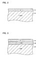
- a C layer 12 formed of carbon is formed on the surface of the n-type GaN layer 10 by sputtering, as shown in FIG. 2 .
- a Ti layer 14 formed of titanium is formed on a surface of the C layer 12 by sputtering.
- the layer 16 of Ti (C, N) which is a complete solid solution of TiC and TiN is formed between the Ti layer 14 and the GaN layer 10 as shown in FIG. 3 .
- the reason for this is believed to be that Ti in the Ti layer 14, C in the C layer 12 and N in the GaN layer 10 undergo reaction due to the heat during sputtering of the Ti layer 14.
- the Ti layer 14 formed in step S6 serves as the electrode of the semiconductor device.
- steps S4 and S6 the C layer 12 and the Ti layer 14 are selectively formed in a region where the electrode should be formed.
- the C layer 12 and the Ti layer 14 may be selectively formed by well-known techniques.
- the Ti layer 14 is formed so as to have a greater thickness than the C layer 12 formed in step S4.
- ohmic contact between the Ti layer 14 and the GaN layer 10 has low contact resistivity.
- the reason for this is believed to be as follows.
- the work function of n-type GaN is about 3.1 eV.
- the work functions of TiC is about 3.5 eV.
- the work function of TiN is about 3.75 eV. Namely, both of TiC and TiN have higher work function than that of n-type GaN. Accordingly, TiC and TiN show ohmic properties on n-type GaN. Therefore, Ti (C, N) which is the complete solid solution of TiC and TiN also shows ohmic properties on n-type GaN. In addition, Ti (C, N) is hard to be segregated because it is complete solid solution.
- step S6 the Ti (C, N) layer 16 is uniformly formed throughout the border of the Ti layer 14 and the GaN layer 10. Accordingly, the Ti layer 14 formed in step S6 is in ohmic contact with the GaN layer 10 throughout the border with the GaN layer 10. Therefore, the Ti layer 14 has smaller contact resistivity to the GaN layer than conventional electrodes which are in ohmic contact with the GaN layer in the form of islands.
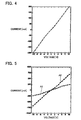
- FIG 4 shows current-voltage characteristics between the Ti layer and the n-type GaN layer when the Ti layer is formed by a conventional method (i.e. a method in which the Ti layer is formed directly on the n-type GaN layer and then the semiconductor substrate is annealed).
- A1 in FIG. 5 represents current-voltage characteristics between the Ti layer 14 and the n-type GaN layer 10 formed by the manufacturing method of the first embodiment. It is found by comparing FIGs. 4 and 5 that the Ti layer 14 formed by the manufacturing method of the first embodiment has lower contact resistivity than the Ti layer formed by the conventional method. Therefore, the Ti layer 14 formed by the manufacturing method of the first embodiment serves as an excellent ohmic electrode.
- steps S2 to S6 are carried out in the same manner as the manufacturing method of the first embodiment.
- the semiconductor substrate is annealed after step S6. In annealing, the semiconductor substrate is maintained at a temperature of about 873 K for about 300 seconds.
- A2 in FIG 5 represents current-voltage characteristics between the Ti layer 14 and the n-type GaN layer 10 formed by the manufacturing method of the second embodiment.
- contact resistivity of the Ti layer 14 to the GaN layer 10 is further decreased by annealing the semiconductor substrate.
- the semiconductor device can be manufactured with an electrode having even lower contact resistivity.
- the semiconductor device can be manufactured with the electrode (i.e. Ti layer 14) having lower contact resistivity to the n-type GaN layer 10 compared to the conventional electrode.
- the Ti layer 14 is in ohmic contact with the GaN layer 10 without annealing the semiconductor substrate after formation of the Ti layer 14.
- the semiconductor device can be manufactured with higher manufacturing efficacy than the conventional method.
- the semiconductor device with the electrode having further lower contact resistivity compared to the first embodiment can be manufactured.
- the Ti layer 14 formed in a greater thickness than the C layer 12 in step S6.
- the whole C layer 12 can undergo reaction so that the Ti (C, N) layer 16 is formed throughout an entire region between the GaN layer 10 and the Ti layer 14. Namely, the C layer 12 is prevented from remaining between the GaN layer 10 and the Ti layer 14. Due to this, the contact resistivity of the Ti layer 14 can further be decreased.
- the C layer 12 was formed by sputtering, but the C layer 12 may alternatively be formed by evaporation or the like.
- the Ti layer 14 was formed by sputtering, but the Ti layer 14 may alternatively be formed by evaporation or the like. Even if the Ti layer 14 is formed by evaporation in the first and second embodiments, lower contact resistivity can be provided.
- the Ti layer 14 was exposed at the surface.
- other metal layer(s) e.g. Al, Ni, Au etc.
- the manufacturing methods of the first and second embodiments can be used for manufacture of various semiconductor devices such as manufacture of LEDs or GaN-based power devices (diodes, transistors etc.).
Landscapes
- Electrodes Of Semiconductors (AREA)
- Junction Field-Effect Transistors (AREA)
Abstract
Description
- The technology described herein relates to a semiconductor device including an electrode in ohmic contact with a nitride semiconductor layer.
- As disclosed in Japanese Patent Application Laid-open No.
2008-235405 - According to the above electrode forming method, the TiN layer is formed in a form of islands at a border of the Ti layer and the GaN layer. Namely, the TiN layer is not formed throughout the border of the Ti layer and the GaN layer, but is formed partially at the border. This is because TiN is segregated at the border of the Ti layer and the GaN layer during the heat treatment. Therefore, according to the above electrode forming method, contact resistivity between the Ti layer and GaN layer is high because of the TiN layer formed in the form of islands at the border of the Ti layer and the GaN layer.
- A semiconductor device including an electrode having low contact resistivity to the nitride semiconductor and a manufacturing method thereof are provided herein.
- A manufacturing method of the semiconductor device disclosed herein includes a carbon containing layer forming step and a titanium containing layer forming step. In the carbon containing layer forming step, a carbon containing layer containing carbon is formed on a nitride semiconductor layer. In the titanium containing layer forming step, a titanium containing layer containing titanium is formed on the carbon containing layer.
- When the titanium containing layer is formed on the carbon containing layer, Ti (C, N) which is a complete solid solution of TiN and TiC is formed from N in the nitride semiconductor layer, C in the carbon containing layer and Ti in the titanium containing layer. Ti (C, N) shows an excellent ohmic property on the nitride semiconductor layer. As Ti (C, N) is a complete solid solution, it is difficult to be segregated. Therefore, the titanium containing layer comes to be in ohmic contact with the nitride semiconductor layer over a broad area. Thus, contact resistivity between the titanium containing layer and the nitride semiconductor layer is lower than conventional electrodes. According to the present manufacturing method, the semiconductor device can be obtained including an electrode (i.e. titanium containing layer) having lower contact resistivity to the nitride semiconductor layer than the conventional electrodes.
- The manufacturing method described above may include an annealing step of heating the semiconductor substrate after the titanium containing layer forming step. When the annealing step is carried out after the titanium containing layer forming step, the contact resistivity between the nitride semiconductor layer and the titanium containing layer is further decreased. The reason for this is believed to be that the reaction of formation of the complete solid solution Ti (C, N) from N in the nitride semiconductor layer, C in the carbon containing layer and Ti in the titanium containing layer is promoted by the annealing step.
- The semiconductor device including an electrode having low contact resistivity to the nitride semiconductor layer is also provided herein. The semiconductor device includes the nitride semiconductor layer, a complete solid solution layer and the titanium containing layer. The complete solid solution layer is formed on the nitride semiconductor layer and formed of a complete solid solution of titanium carbide and titanium nitride. The titanium containing layer is formed on the complete solid solution layer and contains titanium.
- In this semiconductor device, the titanium containing layer is in contact with the nitride semiconductor layer via the complete solid solution layer. Thus, contact resistivity between the titanium containing layer and the nitride semiconductor layer is low. The titanium containing layer serves as an excellent ohmic electrode on the nitride semiconductor layer.
-
-
FIG. 1 is a flowchart showing steps of electrode formation in the manufacturing method of the semiconductor device of a first embodiment; -
FIG. 2 is a sectional view showing the vicinity of a surface of an n-type GaN layer 10 after formation of aC layer 12; -
FIG. 3 is a sectional view showing the vicinity of the surface of the n-type GaN layer 10 after formation of aTi layer 14; -
FIG. 4 is a graph showing current-voltage characteristics of an electrode formed by a conventional method; and -
FIG. 5 is a graph showing current-voltage characteristics of electrodes formed by methods in first and second embodiments. - The manufacturing methods of the semiconductor devices according to embodiments are now described. The present manufacturing methods are characteristic in their step of forming an electrode, and thus descriptions on other steps (steps by which various regions are formed in the semiconductor substrate etc.) are omitted.
- According to the manufacturing method of the first embodiment, an electrode is formed on a surface of a semiconductor substrate following the flowchart in
FIG. 1 . According to the present embodiment, the electrode is formed on a surface of an n-type GaN layer in the semiconductor substrate. In step S2, the surface of the semiconductor substrate is cleaned by sputtering. In step S4, aC layer 12 formed of carbon is formed on the surface of the n-type GaN layer 10 by sputtering, as shown inFIG. 2 . In step S6, aTi layer 14 formed of titanium is formed on a surface of theC layer 12 by sputtering. When theTi layer 14 is formed in step S6, thelayer 16 of Ti (C, N) which is a complete solid solution of TiC and TiN is formed between theTi layer 14 and theGaN layer 10 as shown inFIG. 3 . The reason for this is believed to be that Ti in theTi layer 14, C in theC layer 12 and N in theGaN layer 10 undergo reaction due to the heat during sputtering of theTi layer 14. TheTi layer 14 formed in step S6 serves as the electrode of the semiconductor device. - In steps S4 and S6, the
C layer 12 and theTi layer 14 are selectively formed in a region where the electrode should be formed. TheC layer 12 and theTi layer 14 may be selectively formed by well-known techniques. In step S6, theTi layer 14 is formed so as to have a greater thickness than theC layer 12 formed in step S4. - By formation of the
Ti layer 14, ohmic contact between theTi layer 14 and the GaNlayer 10 has low contact resistivity. The reason for this is believed to be as follows. The work function of n-type GaN is about 3.1 eV. The work functions of TiC is about 3.5 eV. The work function of TiN is about 3.75 eV. Namely, both of TiC and TiN have higher work function than that of n-type GaN. Accordingly, TiC and TiN show ohmic properties on n-type GaN. Therefore, Ti (C, N) which is the complete solid solution of TiC and TiN also shows ohmic properties on n-type GaN. In addition, Ti (C, N) is hard to be segregated because it is complete solid solution. Therefore, in step S6, the Ti (C, N)layer 16 is uniformly formed throughout the border of theTi layer 14 and theGaN layer 10. Accordingly, theTi layer 14 formed in step S6 is in ohmic contact with theGaN layer 10 throughout the border with theGaN layer 10. Therefore, theTi layer 14 has smaller contact resistivity to the GaN layer than conventional electrodes which are in ohmic contact with the GaN layer in the form of islands. -
FIG 4 shows current-voltage characteristics between the Ti layer and the n-type GaN layer when the Ti layer is formed by a conventional method (i.e. a method in which the Ti layer is formed directly on the n-type GaN layer and then the semiconductor substrate is annealed). A1 inFIG. 5 represents current-voltage characteristics between theTi layer 14 and the n-type GaN layer 10 formed by the manufacturing method of the first embodiment. It is found by comparingFIGs. 4 and 5 that theTi layer 14 formed by the manufacturing method of the first embodiment has lower contact resistivity than the Ti layer formed by the conventional method. Therefore, theTi layer 14 formed by the manufacturing method of the first embodiment serves as an excellent ohmic electrode. - The manufacturing method of the semiconductor device of the second embodiment is now described. In the manufacturing method of the second embodiment, steps S2 to S6 are carried out in the same manner as the manufacturing method of the first embodiment. In addition, in the manufacturing method of the second embodiment, the semiconductor substrate is annealed after step S6. In annealing, the semiconductor substrate is maintained at a temperature of about 873 K for about 300 seconds.
- A2 in
FIG 5 represents current-voltage characteristics between theTi layer 14 and the n-type GaN layer 10 formed by the manufacturing method of the second embodiment. As shown inFIG. 5 , contact resistivity of theTi layer 14 to theGaN layer 10 is further decreased by annealing the semiconductor substrate. According to the manufacturing method of the second embodiment, the semiconductor device can be manufactured with an electrode having even lower contact resistivity. - As explained above, according to the manufacturing methods of the first and second embodiments, the semiconductor device can be manufactured with the electrode (i.e. Ti layer 14) having lower contact resistivity to the n-
type GaN layer 10 compared to the conventional electrode. According to the manufacturing method of the first embodiment, theTi layer 14 is in ohmic contact with theGaN layer 10 without annealing the semiconductor substrate after formation of theTi layer 14. Thus, the semiconductor device can be manufactured with higher manufacturing efficacy than the conventional method. According to the manufacturing method of the second embodiment, the semiconductor device with the electrode having further lower contact resistivity compared to the first embodiment can be manufactured. - According to the first and second embodiments described above, the
Ti layer 14 formed in a greater thickness than theC layer 12 in step S6. By forming theTi layer 14 having a greater thickness than theC layer 12, thewhole C layer 12 can undergo reaction so that the Ti (C, N)layer 16 is formed throughout an entire region between theGaN layer 10 and theTi layer 14. Namely, theC layer 12 is prevented from remaining between theGaN layer 10 and theTi layer 14. Due to this, the contact resistivity of theTi layer 14 can further be decreased. - In the first and second embodiments described above, the
C layer 12 was formed by sputtering, but theC layer 12 may alternatively be formed by evaporation or the like. In the first and second embodiments described above, theTi layer 14 was formed by sputtering, but theTi layer 14 may alternatively be formed by evaporation or the like. Even if theTi layer 14 is formed by evaporation in the first and second embodiments, lower contact resistivity can be provided. - In the first and second embodiments described above, the
Ti layer 14 was exposed at the surface. However, other metal layer(s) (e.g. Al, Ni, Au etc.) may be formed on theTi layer 14 to obtain an electrode having a multilayer structure. - The manufacturing methods of the first and second embodiments can be used for manufacture of various semiconductor devices such as manufacture of LEDs or GaN-based power devices (diodes, transistors etc.).
Claims (3)
- A manufacturing method of a semiconductor device, the method comprising:a carbon containing layer forming step of forming a carbon containing layer containing carbon on a nitride semiconductor layer; anda titanium containing layer forming step of forming a titanium containing layer containing titanium on the carbon containing layer.
- The method of claim 1, further comprising an annealing step of heating a semiconductor substrate after the titanium containing layer forming step.
- A semiconductor device comprising:a nitride semiconductor layer;a complete solid solution layer formed on the nitride semiconductor layer and formed of a complete solid solution of titanium carbide and titanium nitride; anda titanium containing layer formed on the complete solid solution layer and containing titanium.
Applications Claiming Priority (2)
| Application Number | Priority Date | Filing Date | Title |
|---|---|---|---|
| JP2009229381A JP5375497B2 (en) | 2009-10-01 | 2009-10-01 | Semiconductor device and method for manufacturing semiconductor device |
| PCT/JP2010/065013 WO2011040172A1 (en) | 2009-10-01 | 2010-09-02 | Semiconductor device, and process for production of semiconductor device |
Publications (3)
| Publication Number | Publication Date |
|---|---|
| EP2485250A1 true EP2485250A1 (en) | 2012-08-08 |
| EP2485250A4 EP2485250A4 (en) | 2013-08-21 |
| EP2485250B1 EP2485250B1 (en) | 2014-07-16 |
Family
ID=43826000
Family Applications (1)
| Application Number | Title | Priority Date | Filing Date |
|---|---|---|---|
| EP10820292.0A Not-in-force EP2485250B1 (en) | 2009-10-01 | 2010-09-02 | Semiconductor device, and process for production of semiconductor device |
Country Status (5)
| Country | Link |
|---|---|
| US (1) | US8633101B2 (en) |
| EP (1) | EP2485250B1 (en) |
| JP (1) | JP5375497B2 (en) |
| CN (1) | CN102668040B (en) |
| WO (1) | WO2011040172A1 (en) |
Cited By (1)
| Publication number | Priority date | Publication date | Assignee | Title |
|---|---|---|---|---|
| EP4220687A1 (en) * | 2022-02-01 | 2023-08-02 | STMicroelectronics S.r.l. | Manufacturing process of an ohmic contact of a hemt device and hemt device |
Families Citing this family (2)
| Publication number | Priority date | Publication date | Assignee | Title |
|---|---|---|---|---|
| CN109979802B (en) * | 2017-12-28 | 2020-12-22 | 中国科学院苏州纳米技术与纳米仿生研究所 | High work function tunable transition metal nitride material, its preparation method and application |
| US20240258370A1 (en) * | 2023-01-31 | 2024-08-01 | Industrial Technology Research Institute | Semiconductor component |
Family Cites Families (32)
| Publication number | Priority date | Publication date | Assignee | Title |
|---|---|---|---|---|
| JP3174135B2 (en) * | 1992-05-07 | 2001-06-11 | シャープ株式会社 | Compound semiconductor device |
| JP3171677B2 (en) * | 1992-07-24 | 2001-05-28 | シャープ株式会社 | Ohmic electrode |
| KR0147626B1 (en) * | 1995-03-30 | 1998-11-02 | 김광호 | Method for forming gate electrode |
| US5929523A (en) * | 1996-03-07 | 1999-07-27 | 3C Semiconductor Corporation | Os rectifying Schottky and ohmic junction and W/WC/TiC ohmic contacts on SiC |
| JPH09266351A (en) | 1996-03-28 | 1997-10-07 | Fuji Photo Film Co Ltd | AlInGaN semiconductor light emitting device |
| US6072818A (en) | 1996-03-28 | 2000-06-06 | Fuji Photo Film Co., Ltd. | Semiconductor light emission device |
| US6340827B1 (en) * | 1999-01-13 | 2002-01-22 | Agere Systems Guardian Corp. | Diffusion barrier for use with high dielectric constant materials and electronic devices incorporating same |
| JP2000315817A (en) * | 1999-04-28 | 2000-11-14 | Matsushita Electronics Industry Corp | Semiconductor device |
| JP4514252B2 (en) * | 1999-07-29 | 2010-07-28 | 古河電気工業株式会社 | GaN-based semiconductor device manufacturing method |
| US6436819B1 (en) * | 2000-02-01 | 2002-08-20 | Applied Materials, Inc. | Nitrogen treatment of a metal nitride/metal stack |
| JP3408527B2 (en) * | 2000-10-26 | 2003-05-19 | 松下電器産業株式会社 | Method for manufacturing semiconductor device |
| US6853076B2 (en) * | 2001-09-21 | 2005-02-08 | Intel Corporation | Copper-containing C4 ball-limiting metallurgy stack for enhanced reliability of packaged structures and method of making same |
| CN100413998C (en) * | 2002-08-08 | 2008-08-27 | 株式会社神户制钢所 | Alumina coating having alpha-type crystal structure as main component, and related technology |
| US7144768B2 (en) * | 2003-06-12 | 2006-12-05 | Juyong Chung | Fabrication of titanium and titanium alloy anode for dielectric and insulated films |
| US7230292B2 (en) * | 2003-08-05 | 2007-06-12 | Micron Technology, Inc. | Stud electrode and process for making same |
| US7170176B2 (en) * | 2003-11-04 | 2007-01-30 | Semiconductor Energy Laboratory Co., Ltd. | Semiconductor device |
| JP4841844B2 (en) | 2005-01-05 | 2011-12-21 | 三菱電機株式会社 | Semiconductor element |
| US7316962B2 (en) * | 2005-01-07 | 2008-01-08 | Infineon Technologies Ag | High dielectric constant materials |
| KR100878433B1 (en) * | 2005-05-18 | 2009-01-13 | 삼성전기주식회사 | Method for manufacturing ohmic contact layer of light emitting device and method for manufacturing light emitting device using same |
| JP2007005764A (en) | 2005-05-27 | 2007-01-11 | Toyota Motor Corp | Semiconductor device and manufacturing method thereof |
| KR101272097B1 (en) * | 2005-06-03 | 2013-06-07 | 가부시키가이샤 한도오따이 에네루기 켄큐쇼 | Integrated circuit device and manufacturing method thereof |
| KR100753152B1 (en) * | 2005-08-12 | 2007-08-30 | 삼성전자주식회사 | Nitride-based light emitting device and its manufacturing method |
| US7795050B2 (en) * | 2005-08-12 | 2010-09-14 | Samsung Electronics Co., Ltd. | Single-crystal nitride-based semiconductor substrate and method of manufacturing high-quality nitride-based light emitting device by using the same |
| JP4991134B2 (en) * | 2005-09-15 | 2012-08-01 | ルネサスエレクトロニクス株式会社 | Semiconductor device and manufacturing method thereof |
| WO2007049939A1 (en) * | 2005-10-29 | 2007-05-03 | Samsung Electronics Co., Ltd. | Semiconductor device and method of fabricating the same |
| JP2008235405A (en) * | 2007-03-19 | 2008-10-02 | Denso Corp | Semiconductor device |
| US7851915B2 (en) * | 2007-04-30 | 2010-12-14 | Stmicroelectronics S.A. | Electronic component comprising a titanium carbonitride (TiCN) barrier layer and process of making the same |
| JP2010021490A (en) * | 2008-07-14 | 2010-01-28 | Kobe Steel Ltd | Semiconductor wiring |
| US7846841B2 (en) * | 2008-09-30 | 2010-12-07 | Tokyo Electron Limited | Method for forming cobalt nitride cap layers |
| JP4415100B1 (en) * | 2008-12-19 | 2010-02-17 | 国立大学法人東北大学 | Copper wiring, semiconductor device, and copper wiring forming method |
| KR101094386B1 (en) * | 2009-11-30 | 2011-12-15 | 주식회사 하이닉스반도체 | Method for manufacturing electrode and capacitor of semiconductor device |
| KR101094375B1 (en) * | 2009-11-30 | 2011-12-15 | 주식회사 하이닉스반도체 | Semiconductor Device Having Carbon-Containing Electrode and Manufacturing Method Thereof |
-
2009
- 2009-10-01 JP JP2009229381A patent/JP5375497B2/en not_active Expired - Fee Related
-
2010
- 2010-09-02 WO PCT/JP2010/065013 patent/WO2011040172A1/en not_active Ceased
- 2010-09-02 US US13/499,652 patent/US8633101B2/en not_active Expired - Fee Related
- 2010-09-02 EP EP10820292.0A patent/EP2485250B1/en not_active Not-in-force
- 2010-09-02 CN CN201080042659.3A patent/CN102668040B/en not_active Expired - Fee Related
Non-Patent Citations (3)
| Title |
|---|
| LUTHER B P ET AL: "TITANIUM AND TITANIUM NITRIDE CONTACTS TO N-TYPE GALLIUM NITRIDE", SEMICONDUCTOR SCIENCE AND TECHNOLOGY, IOP PUBLISHING LTD, GB, vol. 13, no. 11, 1 November 1998 (1998-11-01), pages 1322-1327, XP000783146, ISSN: 0268-1242, DOI: 10.1088/0268-1242/13/11/017 * |
| MAEDA M ET AL: "Formation of ohmic contact layer on n-type gallium nitride by controlling interfacial reaction with titanium", MATERIALS SCIENCE & TECHNOLOGY CONFERENCE AND EXHIBITION 2010, (MS&T 10) : HOUSTON, TEXAS, USA, 17 - 21 OCTOBER 2010 / [BY THE ASSOCIATION FOR IRON & STEEL TECHNOLOGY], RED HOOK, NY : CURRAN, 2011, US, vol. 4, 17 October 2010 (2010-10-17), pages 2732-2742, XP008163316, ISBN: 978-1-61782-032-8 * |
| See also references of WO2011040172A1 * |
Cited By (1)
| Publication number | Priority date | Publication date | Assignee | Title |
|---|---|---|---|---|
| EP4220687A1 (en) * | 2022-02-01 | 2023-08-02 | STMicroelectronics S.r.l. | Manufacturing process of an ohmic contact of a hemt device and hemt device |
Also Published As
| Publication number | Publication date |
|---|---|
| EP2485250A4 (en) | 2013-08-21 |
| US20120217639A1 (en) | 2012-08-30 |
| CN102668040B (en) | 2015-01-28 |
| US8633101B2 (en) | 2014-01-21 |
| JP2011077428A (en) | 2011-04-14 |
| EP2485250B1 (en) | 2014-07-16 |
| JP5375497B2 (en) | 2013-12-25 |
| CN102668040A (en) | 2012-09-12 |
| WO2011040172A1 (en) | 2011-04-07 |
Similar Documents
| Publication | Publication Date | Title |
|---|---|---|
| US8895422B2 (en) | Production of an integrated circuit including electrical contact on SiC | |
| EP2428983B1 (en) | Semiconductor device and method of producing same | |
| US10600921B2 (en) | Silicon carbide semiconductor device and method of manufacturing silicon carbide semiconductor device | |
| EP2518758B1 (en) | Method for forming an n-type contact electrode comprising a group iii nitride semiconductor | |
| CN102859661B (en) | Sic semiconductor device and manufacture method thereof | |
| KR101283774B1 (en) | OHMIC ELECTRODE FOR SiC SEMICONDUCTOR, METHOD FOR MANUFACTURE OF OHMIC ELECTRODE FOR SiC SEMICONDUCTOR, SEMICONDUCTOR DEVICE, AND METHOD FOR MANUFACTURE OF SEMICONDUCTOR DEVICE | |
| JP2013211503A (en) | Sic semiconductor device | |
| CN104303269A (en) | Method for manufacturing silicon carbide semiconductor device | |
| WO2013084620A1 (en) | Method for manufacturing semiconductor device | |
| JP5303948B2 (en) | Ohmic electrode forming method and method of manufacturing field effect transistor | |
| US20200365705A1 (en) | Method of forming ohmic contact for gallium nitride-based compound semiconductor device and gallium nitride-based compound semiconductor device | |
| WO2008018342A1 (en) | Silicon carbide semiconductor device and method for fabricating the same | |
| JP2010086999A (en) | Back electrode for semiconductor device, semiconductor device, and manufacturing method of back electrode for semiconductor device | |
| EP2485250A1 (en) | Semiconductor device, and process for production of semiconductor device | |
| JP2006032456A (en) | Semiconductor element and its manufacturing method | |
| JP2008147294A (en) | Electronic devices | |
| TWI469352B (en) | Tantalum carbide semiconductor device and method of manufacturing same | |
| US20090160054A1 (en) | Nitride semiconductor device and method of manufacturing the same | |
| CN115552634B (en) | Semiconductor device and method for manufacturing the same | |
| KR20180124459A (en) | Ohmic contact and ohmic contact between semiconductor and metal and method for forming the same | |
| CN100544024C (en) | Schottky electrode of nitride semiconductor device and manufacturing method thereof | |
| US20060267128A1 (en) | Schottky barrier diode and method of producing the same | |
| CN117438296A (en) | Method for manufacturing contacts on silicon carbide semiconductor substrate and silicon carbide semiconductor device |
Legal Events
| Date | Code | Title | Description |
|---|---|---|---|
| PUAI | Public reference made under article 153(3) epc to a published international application that has entered the european phase |
Free format text: ORIGINAL CODE: 0009012 |
|
| 17P | Request for examination filed |
Effective date: 20120329 |
|
| AK | Designated contracting states |
Kind code of ref document: A1 Designated state(s): AL AT BE BG CH CY CZ DE DK EE ES FI FR GB GR HR HU IE IS IT LI LT LU LV MC MK MT NL NO PL PT RO SE SI SK SM TR |
|
| RAP1 | Party data changed (applicant data changed or rights of an application transferred) |
Owner name: TOYOTA JIDOSHA KABUSHIKI KAISHA |
|
| DAX | Request for extension of the european patent (deleted) | ||
| RAP1 | Party data changed (applicant data changed or rights of an application transferred) |
Owner name: TOYOTA JIDOSHA KABUSHIKI KAISHA |
|
| REG | Reference to a national code |
Ref country code: DE Ref legal event code: R079 Ref document number: 602010017597 Country of ref document: DE Free format text: PREVIOUS MAIN CLASS: H01L0021280000 Ipc: H01L0021285000 |
|
| A4 | Supplementary search report drawn up and despatched |
Effective date: 20130724 |
|
| RIC1 | Information provided on ipc code assigned before grant |
Ipc: H01L 21/285 20060101AFI20130718BHEP Ipc: H01L 29/812 20060101ALI20130718BHEP Ipc: H01L 33/40 20100101ALI20130718BHEP Ipc: H01L 21/338 20060101ALI20130718BHEP Ipc: H01L 33/32 20100101ALI20130718BHEP Ipc: H01L 29/861 20060101ALI20130718BHEP Ipc: H01L 29/45 20060101ALI20130718BHEP |
|
| GRAP | Despatch of communication of intention to grant a patent |
Free format text: ORIGINAL CODE: EPIDOSNIGR1 |
|
| INTG | Intention to grant announced |
Effective date: 20140210 |
|
| GRAS | Grant fee paid |
Free format text: ORIGINAL CODE: EPIDOSNIGR3 |
|
| GRAA | (expected) grant |
Free format text: ORIGINAL CODE: 0009210 |
|
| AK | Designated contracting states |
Kind code of ref document: B1 Designated state(s): AL AT BE BG CH CY CZ DE DK EE ES FI FR GB GR HR HU IE IS IT LI LT LU LV MC MK MT NL NO PL PT RO SE SI SK SM TR |
|
| REG | Reference to a national code |
Ref country code: GB Ref legal event code: FG4D |
|
| REG | Reference to a national code |
Ref country code: CH Ref legal event code: EP |
|
| REG | Reference to a national code |
Ref country code: IE Ref legal event code: FG4D |
|
| REG | Reference to a national code |
Ref country code: AT Ref legal event code: REF Ref document number: 678084 Country of ref document: AT Kind code of ref document: T Effective date: 20140815 |
|
| REG | Reference to a national code |
Ref country code: DE Ref legal event code: R096 Ref document number: 602010017597 Country of ref document: DE Effective date: 20140828 |
|
| REG | Reference to a national code |
Ref country code: NL Ref legal event code: VDEP Effective date: 20140716 |
|
| REG | Reference to a national code |
Ref country code: AT Ref legal event code: MK05 Ref document number: 678084 Country of ref document: AT Kind code of ref document: T Effective date: 20140716 |
|
| REG | Reference to a national code |
Ref country code: LT Ref legal event code: MG4D |
|
| PG25 | Lapsed in a contracting state [announced via postgrant information from national office to epo] |
Ref country code: SE Free format text: LAPSE BECAUSE OF FAILURE TO SUBMIT A TRANSLATION OF THE DESCRIPTION OR TO PAY THE FEE WITHIN THE PRESCRIBED TIME-LIMIT Effective date: 20140716 Ref country code: NO Free format text: LAPSE BECAUSE OF FAILURE TO SUBMIT A TRANSLATION OF THE DESCRIPTION OR TO PAY THE FEE WITHIN THE PRESCRIBED TIME-LIMIT Effective date: 20141016 Ref country code: LT Free format text: LAPSE BECAUSE OF FAILURE TO SUBMIT A TRANSLATION OF THE DESCRIPTION OR TO PAY THE FEE WITHIN THE PRESCRIBED TIME-LIMIT Effective date: 20140716 Ref country code: PT Free format text: LAPSE BECAUSE OF FAILURE TO SUBMIT A TRANSLATION OF THE DESCRIPTION OR TO PAY THE FEE WITHIN THE PRESCRIBED TIME-LIMIT Effective date: 20141117 Ref country code: GR Free format text: LAPSE BECAUSE OF FAILURE TO SUBMIT A TRANSLATION OF THE DESCRIPTION OR TO PAY THE FEE WITHIN THE PRESCRIBED TIME-LIMIT Effective date: 20141017 Ref country code: FI Free format text: LAPSE BECAUSE OF FAILURE TO SUBMIT A TRANSLATION OF THE DESCRIPTION OR TO PAY THE FEE WITHIN THE PRESCRIBED TIME-LIMIT Effective date: 20140716 Ref country code: BG Free format text: LAPSE BECAUSE OF FAILURE TO SUBMIT A TRANSLATION OF THE DESCRIPTION OR TO PAY THE FEE WITHIN THE PRESCRIBED TIME-LIMIT Effective date: 20141016 Ref country code: ES Free format text: LAPSE BECAUSE OF FAILURE TO SUBMIT A TRANSLATION OF THE DESCRIPTION OR TO PAY THE FEE WITHIN THE PRESCRIBED TIME-LIMIT Effective date: 20140716 |
|
| PG25 | Lapsed in a contracting state [announced via postgrant information from national office to epo] |
Ref country code: LV Free format text: LAPSE BECAUSE OF FAILURE TO SUBMIT A TRANSLATION OF THE DESCRIPTION OR TO PAY THE FEE WITHIN THE PRESCRIBED TIME-LIMIT Effective date: 20140716 Ref country code: NL Free format text: LAPSE BECAUSE OF FAILURE TO SUBMIT A TRANSLATION OF THE DESCRIPTION OR TO PAY THE FEE WITHIN THE PRESCRIBED TIME-LIMIT Effective date: 20140716 Ref country code: CY Free format text: LAPSE BECAUSE OF FAILURE TO SUBMIT A TRANSLATION OF THE DESCRIPTION OR TO PAY THE FEE WITHIN THE PRESCRIBED TIME-LIMIT Effective date: 20140716 Ref country code: IS Free format text: LAPSE BECAUSE OF FAILURE TO SUBMIT A TRANSLATION OF THE DESCRIPTION OR TO PAY THE FEE WITHIN THE PRESCRIBED TIME-LIMIT Effective date: 20141116 Ref country code: AT Free format text: LAPSE BECAUSE OF FAILURE TO SUBMIT A TRANSLATION OF THE DESCRIPTION OR TO PAY THE FEE WITHIN THE PRESCRIBED TIME-LIMIT Effective date: 20140716 Ref country code: PL Free format text: LAPSE BECAUSE OF FAILURE TO SUBMIT A TRANSLATION OF THE DESCRIPTION OR TO PAY THE FEE WITHIN THE PRESCRIBED TIME-LIMIT Effective date: 20140716 |
|
| REG | Reference to a national code |
Ref country code: DE Ref legal event code: R097 Ref document number: 602010017597 Country of ref document: DE |
|
| PG25 | Lapsed in a contracting state [announced via postgrant information from national office to epo] |
Ref country code: RO Free format text: LAPSE BECAUSE OF FAILURE TO SUBMIT A TRANSLATION OF THE DESCRIPTION OR TO PAY THE FEE WITHIN THE PRESCRIBED TIME-LIMIT Effective date: 20140716 Ref country code: CZ Free format text: LAPSE BECAUSE OF FAILURE TO SUBMIT A TRANSLATION OF THE DESCRIPTION OR TO PAY THE FEE WITHIN THE PRESCRIBED TIME-LIMIT Effective date: 20140716 Ref country code: MC Free format text: LAPSE BECAUSE OF FAILURE TO SUBMIT A TRANSLATION OF THE DESCRIPTION OR TO PAY THE FEE WITHIN THE PRESCRIBED TIME-LIMIT Effective date: 20140716 Ref country code: SK Free format text: LAPSE BECAUSE OF FAILURE TO SUBMIT A TRANSLATION OF THE DESCRIPTION OR TO PAY THE FEE WITHIN THE PRESCRIBED TIME-LIMIT Effective date: 20140716 Ref country code: LU Free format text: LAPSE BECAUSE OF FAILURE TO SUBMIT A TRANSLATION OF THE DESCRIPTION OR TO PAY THE FEE WITHIN THE PRESCRIBED TIME-LIMIT Effective date: 20140902 Ref country code: EE Free format text: LAPSE BECAUSE OF FAILURE TO SUBMIT A TRANSLATION OF THE DESCRIPTION OR TO PAY THE FEE WITHIN THE PRESCRIBED TIME-LIMIT Effective date: 20140716 Ref country code: DK Free format text: LAPSE BECAUSE OF FAILURE TO SUBMIT A TRANSLATION OF THE DESCRIPTION OR TO PAY THE FEE WITHIN THE PRESCRIBED TIME-LIMIT Effective date: 20140716 Ref country code: IT Free format text: LAPSE BECAUSE OF FAILURE TO SUBMIT A TRANSLATION OF THE DESCRIPTION OR TO PAY THE FEE WITHIN THE PRESCRIBED TIME-LIMIT Effective date: 20140716 |
|
| REG | Reference to a national code |
Ref country code: CH Ref legal event code: PL |
|
| PLBE | No opposition filed within time limit |
Free format text: ORIGINAL CODE: 0009261 |
|
| STAA | Information on the status of an ep patent application or granted ep patent |
Free format text: STATUS: NO OPPOSITION FILED WITHIN TIME LIMIT |
|
| REG | Reference to a national code |
Ref country code: DE Ref legal event code: R084 Ref document number: 602010017597 Country of ref document: DE |
|
| REG | Reference to a national code |
Ref country code: IE Ref legal event code: MM4A |
|
| 26N | No opposition filed |
Effective date: 20150417 |
|
| GBPC | Gb: european patent ceased through non-payment of renewal fee |
Effective date: 20141016 |
|
| REG | Reference to a national code |
Ref country code: FR Ref legal event code: ST Effective date: 20150529 |
|
| PG25 | Lapsed in a contracting state [announced via postgrant information from national office to epo] |
Ref country code: BE Free format text: LAPSE BECAUSE OF NON-PAYMENT OF DUE FEES Effective date: 20140930 |
|
| PG25 | Lapsed in a contracting state [announced via postgrant information from national office to epo] |
Ref country code: LI Free format text: LAPSE BECAUSE OF NON-PAYMENT OF DUE FEES Effective date: 20140930 Ref country code: GB Free format text: LAPSE BECAUSE OF NON-PAYMENT OF DUE FEES Effective date: 20141016 Ref country code: CH Free format text: LAPSE BECAUSE OF NON-PAYMENT OF DUE FEES Effective date: 20140930 |
|
| PG25 | Lapsed in a contracting state [announced via postgrant information from national office to epo] |
Ref country code: IE Free format text: LAPSE BECAUSE OF NON-PAYMENT OF DUE FEES Effective date: 20140902 Ref country code: FR Free format text: LAPSE BECAUSE OF NON-PAYMENT OF DUE FEES Effective date: 20140930 |
|
| PG25 | Lapsed in a contracting state [announced via postgrant information from national office to epo] |
Ref country code: SI Free format text: LAPSE BECAUSE OF FAILURE TO SUBMIT A TRANSLATION OF THE DESCRIPTION OR TO PAY THE FEE WITHIN THE PRESCRIBED TIME-LIMIT Effective date: 20140716 |
|
| PG25 | Lapsed in a contracting state [announced via postgrant information from national office to epo] |
Ref country code: SM Free format text: LAPSE BECAUSE OF FAILURE TO SUBMIT A TRANSLATION OF THE DESCRIPTION OR TO PAY THE FEE WITHIN THE PRESCRIBED TIME-LIMIT Effective date: 20140716 |
|
| PG25 | Lapsed in a contracting state [announced via postgrant information from national office to epo] |
Ref country code: MT Free format text: LAPSE BECAUSE OF FAILURE TO SUBMIT A TRANSLATION OF THE DESCRIPTION OR TO PAY THE FEE WITHIN THE PRESCRIBED TIME-LIMIT Effective date: 20140716 |
|
| PG25 | Lapsed in a contracting state [announced via postgrant information from national office to epo] |
Ref country code: BE Free format text: LAPSE BECAUSE OF FAILURE TO SUBMIT A TRANSLATION OF THE DESCRIPTION OR TO PAY THE FEE WITHIN THE PRESCRIBED TIME-LIMIT Effective date: 20140716 Ref country code: HR Free format text: LAPSE BECAUSE OF FAILURE TO SUBMIT A TRANSLATION OF THE DESCRIPTION OR TO PAY THE FEE WITHIN THE PRESCRIBED TIME-LIMIT Effective date: 20140716 Ref country code: TR Free format text: LAPSE BECAUSE OF FAILURE TO SUBMIT A TRANSLATION OF THE DESCRIPTION OR TO PAY THE FEE WITHIN THE PRESCRIBED TIME-LIMIT Effective date: 20140716 Ref country code: HU Free format text: LAPSE BECAUSE OF FAILURE TO SUBMIT A TRANSLATION OF THE DESCRIPTION OR TO PAY THE FEE WITHIN THE PRESCRIBED TIME-LIMIT; INVALID AB INITIO Effective date: 20100902 |
|
| PG25 | Lapsed in a contracting state [announced via postgrant information from national office to epo] |
Ref country code: MK Free format text: LAPSE BECAUSE OF FAILURE TO SUBMIT A TRANSLATION OF THE DESCRIPTION OR TO PAY THE FEE WITHIN THE PRESCRIBED TIME-LIMIT Effective date: 20140716 |
|
| PG25 | Lapsed in a contracting state [announced via postgrant information from national office to epo] |
Ref country code: AL Free format text: LAPSE BECAUSE OF FAILURE TO SUBMIT A TRANSLATION OF THE DESCRIPTION OR TO PAY THE FEE WITHIN THE PRESCRIBED TIME-LIMIT Effective date: 20140716 |
|
| REG | Reference to a national code |
Ref country code: DE Ref legal event code: R082 Ref document number: 602010017597 Country of ref document: DE Representative=s name: TBK, DE Ref country code: DE Ref legal event code: R081 Ref document number: 602010017597 Country of ref document: DE Owner name: DENSO CORP., KARIYA-CITY, JP Free format text: FORMER OWNER: TOYOTA JIDOSHA KABUSHIKI KAISHA, TOYOTA-SHI, AICHI-KEN, JP |
|
| PGFP | Annual fee paid to national office [announced via postgrant information from national office to epo] |
Ref country code: DE Payment date: 20220620 Year of fee payment: 13 |
|
| REG | Reference to a national code |
Ref country code: DE Ref legal event code: R119 Ref document number: 602010017597 Country of ref document: DE |
|
| PG25 | Lapsed in a contracting state [announced via postgrant information from national office to epo] |
Ref country code: DE Free format text: LAPSE BECAUSE OF NON-PAYMENT OF DUE FEES Effective date: 20240403 |