EP2482129A1 - Vibration member driving circuit - Google Patents
Vibration member driving circuit Download PDFInfo
- Publication number
- EP2482129A1 EP2482129A1 EP12150048A EP12150048A EP2482129A1 EP 2482129 A1 EP2482129 A1 EP 2482129A1 EP 12150048 A EP12150048 A EP 12150048A EP 12150048 A EP12150048 A EP 12150048A EP 2482129 A1 EP2482129 A1 EP 2482129A1
- Authority
- EP
- European Patent Office
- Prior art keywords
- vibration member
- vibration
- driving circuit
- vibrations
- electro
- Prior art date
- Legal status (The legal status is an assumption and is not a legal conclusion. Google has not performed a legal analysis and makes no representation as to the accuracy of the status listed.)
- Granted
Links
Images








Classifications
-
- G—PHYSICS
- G02—OPTICS
- G02B—OPTICAL ELEMENTS, SYSTEMS OR APPARATUS
- G02B27/00—Optical systems or apparatus not provided for by any of the groups G02B1/00 - G02B26/00, G02B30/00
- G02B27/0006—Optical systems or apparatus not provided for by any of the groups G02B1/00 - G02B26/00, G02B30/00 with means to keep optical surfaces clean, e.g. by preventing or removing dirt, stains, contamination, condensation
-
- B—PERFORMING OPERATIONS; TRANSPORTING
- B06—GENERATING OR TRANSMITTING MECHANICAL VIBRATIONS IN GENERAL
- B06B—METHODS OR APPARATUS FOR GENERATING OR TRANSMITTING MECHANICAL VIBRATIONS OF INFRASONIC, SONIC, OR ULTRASONIC FREQUENCY, e.g. FOR PERFORMING MECHANICAL WORK IN GENERAL
- B06B1/00—Methods or apparatus for generating mechanical vibrations of infrasonic, sonic, or ultrasonic frequency
- B06B1/02—Methods or apparatus for generating mechanical vibrations of infrasonic, sonic, or ultrasonic frequency making use of electrical energy
- B06B1/0207—Driving circuits
- B06B1/0215—Driving circuits for generating pulses, e.g. bursts of oscillations, envelopes
-
- G—PHYSICS
- G03—PHOTOGRAPHY; CINEMATOGRAPHY; ANALOGOUS TECHNIQUES USING WAVES OTHER THAN OPTICAL WAVES; ELECTROGRAPHY; HOLOGRAPHY
- G03B—APPARATUS OR ARRANGEMENTS FOR TAKING PHOTOGRAPHS OR FOR PROJECTING OR VIEWING THEM; APPARATUS OR ARRANGEMENTS EMPLOYING ANALOGOUS TECHNIQUES USING WAVES OTHER THAN OPTICAL WAVES; ACCESSORIES THEREFOR
- G03B17/00—Details of cameras or camera bodies; Accessories therefor
- G03B17/02—Bodies
-
- H—ELECTRICITY
- H02—GENERATION; CONVERSION OR DISTRIBUTION OF ELECTRIC POWER
- H02P—CONTROL OR REGULATION OF ELECTRIC MOTORS, ELECTRIC GENERATORS OR DYNAMO-ELECTRIC CONVERTERS; CONTROLLING TRANSFORMERS, REACTORS OR CHOKE COILS
- H02P31/00—Arrangements for regulating or controlling electric motors not provided for in groups H02P1/00 - H02P5/00, H02P7/00 or H02P21/00 - H02P29/00
-
- H—ELECTRICITY
- H04—ELECTRIC COMMUNICATION TECHNIQUE
- H04N—PICTORIAL COMMUNICATION, e.g. TELEVISION
- H04N23/00—Cameras or camera modules comprising electronic image sensors; Control thereof
- H04N23/50—Constructional details
- H04N23/52—Elements optimising image sensor operation, e.g. for electromagnetic interference [EMI] protection or temperature control by heat transfer or cooling elements
-
- H—ELECTRICITY
- H04—ELECTRIC COMMUNICATION TECHNIQUE
- H04N—PICTORIAL COMMUNICATION, e.g. TELEVISION
- H04N23/00—Cameras or camera modules comprising electronic image sensors; Control thereof
- H04N23/80—Camera processing pipelines; Components thereof
- H04N23/81—Camera processing pipelines; Components thereof for suppressing or minimising disturbance in the image signal generation
- H04N23/811—Camera processing pipelines; Components thereof for suppressing or minimising disturbance in the image signal generation by dust removal, e.g. from surfaces of the image sensor or processing of the image signal output by the electronic image sensor
Definitions
- Embodiments of the present invention relate to vibration member driving circuits.
- An image pickup unit of a copy machine or facsimile machine as an optical apparatus scans a line sensor or scans a document placed closer to a line sensor to read a flat document.
- the dust appears on a scanned image.
- One piece of dust may appear as a line image which continues in a document feeding direction and deteriorates the quality of the image in a reading unit of a facsimile machine which scans and reads a document or a reading unit of a copy machine which reads, that is, skims a document during transport from an automatic document feeder.
- FIG. 3 is a schematic diagram illustrating a configuration of a dust removing device disclosed in Japanese Patent Laid-Open No. 2008-207170 .
- a vibration member 501 having an optical member 502 is provided on a light entrance side of an image pickup element 503.
- Piezoelectric elements 101a and 101b which are electro-mechanical energy conversion elements are placed at different positions in the direction where nodal lines of out-of-plane bending vibration are aligned in the vibration member 501. Alternating voltages having an equal frequency and a phase difference of 90° are applied to the piezoelectric elements 101a and 101b.
- the frequency of the alternating voltage to be applied is between a resonance frequency in an m-order (where m is a natural number) vibration mode which bends out of plane along the longitudinal direction of the vibration member 501 and a resonance frequency in an (m + 1)-order vibration mode.
- vibrations in the m-order vibration mode with a response with a resonance phenomenon and vibrations in the (m + 1)-order vibration mode with a 90° time phase difference (phase advanced by 90° from the m-order out-of-plane bending vibration) are excited with an equal amplitude and at equal vibration periods.
- synthesized vibrations free-traveling waves
- the synthesized vibrations move the dust on the surface of the vibration member 501 in a desirable direction.
- the amplitude change of alternating voltage to be applied to the piezoelectric element 101 may increase near the resonance frequency of the vibration member 501 in some frequency band to be used.
- the alternating voltage largely changes when the resonance frequency of the vibration member 501 varies because of individual differences or the heat while the device is being driven changes the resonance frequency.
- the alternating voltage increased more than necessary may increase the power consumption because of a current increase or damage the optical member 501 because of the increase of the vibration amplitude excited in the vibration member 501.
- the alternating voltage is lower than necessary voltage, a sufficient vibration amplitude of the out-of-plane bending vibration to be excited in the vibration member 501 may not be acquired, and the dust removal efficiency may decrease.
- One disclosed aspect of the embodiments provides a driving circuit which outputs a stable voltage amplitude in a used frequency band with a small change in alternating voltage to be applied to an electro-mechanical energy conversion element even when the resonance frequency of a vibration member varies or changes during the device is being driven.
- One embodiment in its first aspect provides a vibration member driving circuit as specified in claim 1.
- a driving circuit may be provided which outputs a stable voltage amplitude in a used frequency band with a small change in alternating voltage to be applied to an electro-mechanical energy conversion element even when the resonance frequency of a vibration member varies or changes during the device is being driven.
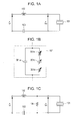
- FIGs. 1A to 1C illustrate a vibration member driving circuit according to a first embodiment.
- FIGs. 2A and 2B are perspective view of an image pickup apparatus to which one embodiment is applicable.
- FIG. 3 is a perspective view illustrating a structure of an image pickup unit of a camera body having a dust removing device.
- FIG. 4 illustrates a control apparatus for the dust removing device to which one embodiment is applicable.
- FIG. 5 illustrates a configuration of a driving circuit in the past.
- FIGs. 6A and 6B are graphs illustrating the frequencies of alternating voltages applied to piezoelectric elements, the amplitude of vibrations occurring in the piezoelectric elements, and their waveforms according to the first embodiment.
- FIG. 7 illustrates the displacement of order 10 out-of-plane bending vibrations and the displacement of order 11 out-of-plane bending vibrations which are excited in the vibration member and bend out of plane along the longitudinal direction and illustrating the arrangement of the piezoelectric elements.
- FIG. 8 illustrates a frequency characteristic of the voltage amplitude of the alternating voltage Vo when a driving circuit in the past is used.
- FIGs. 9A and 9B illustrate a simulation result describing frequency characteristics of a current amplitude and alternating voltages Vo when the series resonance frequency fs with the inductor and capacitor is substantially matched with the resonance frequency fm of the vibration member.
- FIGs. 10A and 10B illustrate results of simulations by calculations of how the alternating voltages Vo change in accordance with the changes in admittance.
- FIGs. 11A and 11B illustrate simulation results of how the alternating voltage Vo changes in accordance with the variations in the inductor, capacitor and the inherent capacitance of the piezoelectric element.
- FIG. 12 illustrates results of measurement of changes in power supply current against driving time.
- FIG. 13 illustrates the frequency characteristic of the alternating voltage Vo when the relationship fe ⁇ 2*fd is satisfied.
- FIGs. 14A and 14B illustrate simulation results describing changes in phase and alternating voltage Vo, compared with the past, in accordance with changes in fs/fm.
- FIG. 15 illustrates simulation results of the proportion of the amounts of changes in phase to the configuration of the example in the past in accordance with changes in fs/fm.
- FIG. 16 illustrates a relationship between the inductance L of the inductor according to the peak frequency fe and the capacitance C of the capacitor.
- FIGs. 17A to 17E illustrate driving circuits for a dust removing device having a transformer according to a second embodiment.
- FIGs. 18A and 18B are graphs illustrating frequency of alternating voltages to be applied to a piezoelectric element driven by standing waves, amplitudes of vibrations occurring in the piezoelectric element and voltage waveforms according to a third embodiments.
- a vibration member driving circuit of one embodiment may drive an object such as powder by vibrating a vibration member.
- One embodiment is applicable if a vibration member is vibrated to drive an object such as powder on the vibration member though a dust removing device for removing dust which is powder and a driving circuit therefor will be described according to embodiments below.
- powder refers to an 1 ⁇ m or larger to 100 ⁇ m or smaller object.
- Apparatuses having a vibration member and/or a driving circuit therefor of the embodiments may include optical apparatuses such as a camera (image pickup device), a facsimile machine, a scanner, a projector, a copy machine, and a printer.
- a vibration member and/or a driving circuit therefor of the embodiments are provided in an image pickup apparatus in embodiments below, for example.
- an image pickup element such as a CCD and a CMOS sensor or a line sensor used in a copier or a facsimile machine, which is a photoelectric conversion element, is called a light receiving element.
- a dust removing device which excites traveling waves in a vibration member to move dust which is powder is mounted in a camera.
- FIG. 2A is a front perspective view, from the subject side, of a digital single-lens reflex camera which is an image pickup apparatus according to the first embodiment and illustrates a state without an imaging lens.
- FIG. 2B is a back perspective view of the camera from a photographer.
- a mirror box 202 is provided to which a imaging luminous flux passed through an imaging lens, not illustrated, is guided.
- a main mirror (quick return mirror) 203 is provided within the mirror box 202.
- An image pickup unit having the dust removing device is provided on an imaging optical axis passed through the imaging lens, not illustrated.
- the main mirror 203 may be held at an angle of 45° about an imaging optical axis so that a photographer may observe a subject image through a finder eye window 204 or may be held at a position avoiding an imaging luminous flux for guiding toward the image pickup element.
- a cleaning instruction switch 205 is provided on the back of the camera and may be used for driving a vibration member which is the dust removing device. If a photographer presses the cleaning instruction switch 205, an instruction unit 604 (refer to FIG. 4 ) is instructed to drive the dust removing device.
- FIG. 3 is a perspective view illustrating a structure of an image pickup unit of the camera body 201 having a dust removing device that is a vibration member.
- An image pickup element 503 is provided in the image pickup unit of the camera body 201.
- the image pickup element 503 is a light receiving element such as a CCD and a CMOS sensor which converts a received subject image to an electric signal.
- a vibration member 501 is attached so as to tightly seal the space on the front surface of the image pickup element 503.
- the vibration member 501 at least includes a rectangular planer optical member 502 which is an elastic body and a pair of piezoelectric element 101a (first electro-mechanical energy conversion element) and a piezoelectric element 101b (second electro-mechanical energy conversion element) which are electro-mechanical energy conversion elements adhered to both ends of the optical member 502.
- the optical member 502 is an optical member with a high transmittance such as a cover glass, infrared cut filter, or an optical low pass filter. Light passing through the optical member 502 enters to the image pickup element 503.
- the dimension in the thickness direction (vertical direction in the drawing) of the piezoelectric elements 101a and 101b at both ends of the optical member 502 is equal to the dimension in the thickness direction (vertical direction in the drawing) of the optical member 502 so as to increase the generative force of the bending deformation against vibrations.
- the piezoelectric elements 101a and 101b will simply be called piezoelectric elements 101 when no distinction is particularly required.
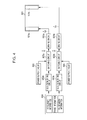
- FIG. 4 illustrates a control apparatus for the dust removing device.
- the control apparatus includes the instruction unit 604, pulse generating circuits 603a and 603b, switching circuits 602a and 602b, a power supply circuit 605, and driving circuits 601a and 601b. From the instruction unit 604, frequency information, phase information, and pulse width information which are parameters of an alternating voltage signal, are transmitted to the pulse generating circuits 603a and 603b.
- the pulse generating circuit may generally be digital oscillators, for example.
- the frequency is set in the vicinity of an intermediate value of the resonance frequency of vibrations (out-of-plane bending vibrations) in two vibration modes generated in the vibration member 501, and equal frequencies are set to the pulse generating circuits 603a and 603b.
- the vibration modes will be described below with reference to FIG. 7 .
- Different values of phases from each other are input to the pulse generating circuits 603a and 603b and are set such that a different phase difference of the alternating voltage signals may be output (such as phase difference of 90°).
- the pulse width (pulse duty) is adjusted properly to acquire a desirable voltage amplitude and is separately set to the pulse generating circuits 603a and 603b.
- the digital alternating voltage signal output from the pulse generating circuit 603 is input to the switching circuits 602a and 602b and is output as an analog alternating voltage Vi on the basis of the voltage supplied from the power supply circuit 605.
- the power supply circuit may be a general DC power supply circuit, DC-DC converter circuit or the like.
- the switching circuit may be a general H-bridge circuit.
- the alternating voltage Vi is input to the driving circuits 601a and 601b and is output as an alternating voltage Vo after its voltage amplitude is raised and is converted to an SIN waveform.
- the output alternating voltage Vo is applied to the piezoelectric elements 101a and 101b, and two out-of-plane bending vibrations simultaneously occur in the vibration member 501.
- the synthesized vibrations become traveling waves and may move dust on the surface of the optical member 502 in a desirable direction.
- the configuration of the driving circuits 601a and 601b which is a characteristic of the embodiments, will be described below with reference to FIG. 1 .
- the digital alternating voltage signal output from the pulse generating circuit 603 is input to the switching circuits 602a and 602b and is output as an analog alternating voltage Vi on the basis of voltage supplied from the power supply circuit 605.
- the power supply circuit may be a general DC power supply circuit, DC-DC converter circuit or the like.
- the switching circuit may be a general H bridge circuit.
- the alternating voltage Vi is input to the driving circuits 601a and 601b and is output as an alternating voltage Vo after its voltage amplitude is raised and is converted to an SIN waveform.
- the alternating voltage Vo is applied to the piezoelectric elements 101a and 101b, and two out-of-plane bending vibrations simultaneously occur in the vibration member 501.
- the synthesized vibrations become traveling waves and may move dust on the surface of the optical member 502 in a desirable direction.
- FIG. 6A is a graph illustrating the frequencies of alternating voltages applied to the piezoelectric elements 101 and the amplitude of vibrations occurring in the piezoelectric elements 101.
- f(m) is a resonance frequency of m-order out-of-plane bending vibrations
- f(m + 1) is a resonance frequency of (m + 1)-order out-of-plane bending vibrations.
- a frequency fd of alternating voltage to be applied to the piezoelectric element 101 is set to f(m) ⁇ fd ⁇ f(m + 1), vibrations at the frequency fd are acquired with an amplitude extended by the resonance phenomenon of the m-order out-of-plane bending vibrations and (m + 1)-order out-of-plane bending vibrations. The time periods of the vibrations are equal.
- the frequency fd of the alternating voltage to be applied to the piezoelectric element 101 is set lower than f(m), the amplitude of the (m + 1)-order out-of-plane bending vibrations is lower.
- the frequency fd is set higher than f(m + 1), the amplitude of the m-order out-of-plane bending vibrations is lower.
- FIG. 7 is a schematic diagram illustrating the displacement of order 10 out-of-plane bending vibrations and the displacement of order 11 out-of-plane bending vibrations which are excited in the vibration member 501 and bend out of plane along the longitudinal direction and illustrating the arrangement of the piezoelectric elements 101a and 101b.
- the horizontal axis indicate the longitudinal position of the vibration member 501.
- the vertical axis indicates the out-of-plane vibration displacement.
- the order 10 out-of-plane bending vibration is indicated by a waveform A (solid line) as a first vibration mode
- the order 11 out-of-plane bending vibration is indicated by a waveform B (broken line) as a second vibration mode.
- the first vibration mode A and second vibration mode B are an out-of-plane bending vibration mode, which bending deforms the vibration member 501 in the thickness direction of the optical member 502.
- the vibrations in the first vibration mode A and second vibration mode B thus simultaneously occur in the vibration member 501 and are superposed.
- the vibration modes minimum required for removing dust are the order 10 bending vibration mode as the first vibration mode and the order 11 bending vibration mode as the second vibration mode.
- the vibration modes are not limited thereto.
- the optical effective area corresponding to the image pickup element 503 is the range illustrated in FIG. 7 .
- the deformed shape in the first vibration mode A has opposite phases (with a phase difference of 180°) at left and right ends.
- the deformed shape in the second vibration mode B is in phase between the left and right ends (with a phase difference of 0°).
- the phase difference between alternating voltages to be applied to the piezoelectric element 101a and piezoelectric element 101b is set to 180°, the first vibration mode A only occurs. If the phase difference is set to 0° on the other hand, the second vibration mode B only occurs.
- the phase difference is set to 90°, the first vibration mode A and second vibration mode B may be caused simultaneously, and the traveling waves from the synthesized vibrations may occur in the right direction of FIG. 7 .
- FIG. 6B illustrates examples of alternating voltages to be applied to the piezoelectric elements for simultaneously exciting vibration modes of different orders.
- the alternating voltage Vo 1 is a voltage waveform to be applied to the piezoelectric element 101a
- the alternating voltage Vo 2 is a voltage waveform to be applied to the piezoelectric element 101b.
- the vertical axis indicates voltage amplitude
- the horizontal axis indicates time.
- the frequency of the alternating voltages Vo 1 and Vo 2 is constant at fd described above, and the phase difference between the alternating voltages is 90°.
- the alternating voltages Vo 1 and Vo 2 may only be required to have different phases, and the phase difference is not limited to 90°.
- the dust adhered to the surface of the optical member 502 moves as if it bounces off under the force in the normal direction of the surface of the optical member 502 when the optical member 502 pushes up the dust out of plane.
- the speed of the synthesized vibration displacement of the vibration member 501 in phases of a drive frequency period is positive, the dust is pushed up out of plane, and the dust moves under the force in the normal direction of the synthesized vibration displacement in the phase.
- the dust may be moved and removed in the right direction of FIG. 7 .
- FIG. 1A illustrates a driving circuit for the dust removing device according to the first embodiment.
- the driving circuit includes an inductor 102 and a capacitor 103 which are serially connected to the piezoelectric element 101.
- the capacitor 103 is connected to the lower side of the piezoelectric element 101 in FIG. 1 , it may be connected to the upper side (between the inductor 102 and the piezoelectric element 101).
- a resistance 104 may be connected in parallel with the piezoelectric element 101.
- the resistance 104 may be set to 1 M ⁇ with which current hardly flows to prevent power consumption in the resistance part.
- Providing the resistance 104 may define the potential at the connection point between the capacitor 103 and the piezoelectric element 101, stable alternating voltages may be applied across the piezoelectric elements.
- the inductor 102 may be an inductance element such as a coil.
- the capacitor 103 may be a capacitance element such as a film capacitor.
- One disclosed aspect of the embodiments is characterized in that the series resonance frequency of the inductor 102 and the capacitor 103 is substantially matched with the resonance frequency of the vibration member 501 (set within a tolerance, which will be described below).
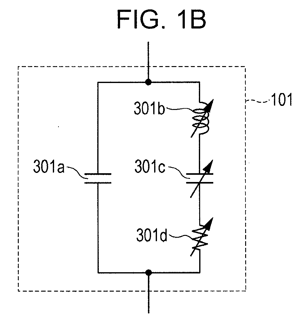
- FIG. 1B illustrates an equivalent circuit of the piezoelectric element 101.
- the equivalent circuit of the piezoelectric element 101 includes an RLC series circuits (equivalent coil 301b of self-inductance Lm, equivalent capacitor 301c of capacitance Cm, and equivalent resistance 301d of resistance value Rm) of the mechanical vibration part of the vibration member 501 and a capacitor 301a functioning as inherent capacitance Cd of the piezoelectric element 101 connected to the RLC series circuit in parallel.
- RLC series circuits equivalent coil 301b of self-inductance Lm, equivalent capacitor 301c of capacitance Cm, and equivalent resistance 301d of resistance value Rm
- the series resonance frequency by the inductor 102 and capacitor 103 is defined as fs
- the resonance frequency of the vibration member 501 is defined as fm.
- the substantially matched fs and fm allows a gentle frequency characteristic of the alternating voltage Vo near fm.
- serially connecting the inductor 102 to the piezoelectric element 101 may form an LC series resonance circuit by the inherent capacitance of the piezoelectric element 101 and the inductor 102.
- the voltage amplitude of the alternating voltage Vi is boosted to a desirable voltage by the LC series resonance circuit, and the alternating voltage Vo is output.
- FIG. 8 illustrates a frequency characteristic of the voltage amplitude of the alternating voltage Vo when a driving circuit in the past is used.
- the horizontal axis indicates frequency, and the vertical axis indicates voltage amplitude.
- the plots indicate a characteristic caused when the value of the inductor 102 is changed from 40 ⁇ H to 90 ⁇ H.
- f(m) is a resonance frequency of an m-order out-of-plane bending vibrations
- f(m + 1) is a resonance frequency of an (m + 1)-order out-of-plane bending vibrations.
- the frequency fd of the alternating voltage Vo to be applied to the piezoelectric element 101 is set to f(m) ⁇ fd ⁇ f(m + 1).
- FIG. 8 illustrates that the amplitude change of the alternating voltage Vo occurs near fm and f(m + 1).
- the change in voltage amplitude increases near fm, f(m + 1) and fd.
- the change in voltage amplitude decreases.
- a desirable voltage amplitude may not be acquired because of the decreasing voltage boost rate.
- the electric resonance frequency fe of the LC series circuit shifts to a higher frequency.
- the harmonics component of the drive frequency fd is superposed over the fundamental harmonic, distorting the waveform. A large waveform distortion may excite unnecessary vibrations in the vibration member 501.
- the reason why the amplitude change of the alternating voltage Vo occurs near fm or f(m + 1) is because the self-inductance Lm and capacitance Cm of the mechanical vibration part of the vibration member 501 cause a change in impedance.
- fs and fm are substantially matched for impedance matching in the mechanical vibration part of the vibration member 501.
- the amplitude change of the alternating voltage Vo may be reduced.
- the gentle frequency characteristic of the alternating voltage Vo near fm may reduce the change in admittance (equivalent resistance 301d) and/or the change in alternating voltage Vo due to the variations in inductor 102 and capacitor 103. Because of the impedance matching of the mechanical vibration part of the vibration member 501, the frequency characteristic is hardly influenced by variations of elements near fm.
- FIGs. 9A and 9B illustrate simulation results describing frequency characteristics of the alternating voltages Vo when the series resonance frequency fs with the inductor 102 and capacitor 103 is substantially matched with the resonance frequency fm of the vibration member 501.
- the driving circuit has the configuration in FIG. 1A .
- the vibration member 501 of this embodiment has two out-of-plane bending vibrations, and the resonance frequencies fm include two of f(m) and f(m + 1).
- fs is set to a lower value than fm because raising the voltage boost rate of the voltage amplitude is difficult.
- the voltage boost rate tends to increase.
- the voltage boost rate tends to decrease.
- the series resonance frequency fs is matched with f(m), the desirable effect may be acquired when it is a frequency near f(m + 1).
- the self-inductance Lm of the equivalent coil 301b was set to 0.04 H, and the capacitance Cm of the equivalent capacitor 301c was set to 44 pF.
- f(m) was set to 120 kHz, and f(m + 1) was set to 128 kHz, and the drive frequency fd was set to 123 kHz.
- An example in the past is also illustrated as a comparison example in which the inductor 102 was set to 68 ⁇ H when the configuration of the driving circuit in FIG. 5 is used. (Stabilizing Voltage)
- FIG. 9A illustrates a frequency characteristic of the current amplitude to be fed to the driving circuit.
- FIG. 9B illustrates a frequency characteristic of the voltage amplitude of the alternating voltage Vo.
- substantially matching between fs and fm may provide a gentle frequency characteristic of the alternating voltage Vo near f(m) and f(m + 1).
- stable voltage is applied to a change in resonance frequency of the vibration member 501, which may reduce changes in drive current. For example, when the resonance frequency f(m + 1) decreases over time during driving, the amplitude of the alternating voltage increases and the drive current increases in the example in the past. According to one embodiment, the changes may be reduced.
- the electric resonance by the inductor 102 and the capacitor 301a which is an inherent capacitance of the capacitor 103 and piezoelectric element 101 may be used to set the amplitude of the alternating voltage Vo to have a peak at a certain frequency. Defining the peak frequency of the alternating voltage Vo as fe and setting fe to a higher frequency than fm may provide a frequency characteristic with less voltage change even when the drive frequency fd of the vibration member 501 is changed in the frequency band from fm to fe. According to this embodiment, all of the peak frequencies fe were set to the range from 180 to 200 kHz.
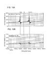
- FIGs. 10A and 10B illustrate the effects of reduction of changes of the alternating voltage Vo.
- FIGs. 10A and 10B illustrate the results of simulations by calculations of how the alternating voltage Vo changes in accordance with the changes in admittance. The changes in admittance were calculated by changing the value of the equivalent resistance 301d from 10% to 100% of a reference value. As the equivalent resistance decreases, the admittance increases.
- FIG. 10A illustrates an example in the past
- FIG. 10B illustrates this embodiment.
- FIGs. 10A and 10B illustrate that this embodiment reduced the influence of a change in admittance to about 20% of that of the example in the past.
- FIGs. 11A and 11B illustrate simulation results of how the alternating voltage Vo changes in accordance with the variations in the inductor 102, capacitor 103 and the inherent capacitance of the piezoelectric element 101. Random number calculation was performed on a uniform distribution by Monte Carlo method when the variation of the self-inductance L of the inductor 102 is ⁇ 20%, the variation of the capacitance C of the capacitor 103 is ⁇ 10%, and the variation of the capacitor 301a which is the inherent capacitance Cd of the piezoelectric element 101 is ⁇ 10%.
- FIG. 11A illustrates an example in the past
- FIG. 11B illustrates this embodiment. According to this embodiment, the influence of the variations of elements of the entire driving circuit including the piezoelectric element 101 is reduced to about 70% of that of the example in the past.
- FIG. 12 illustrates results of measurement of changes in power supply current against driving time.
- the power supply used was 12 VDC power supply.
- the power supply current increased about twice as the initial value after 20 seconds.
- the increase was about 40%. Thus, the power consumption may be reduced.
- fm and fs are completely matched.
- the embodiments are not limited to the case where fs and fm are completely matched.
- fs and fm may be set to close values within a certain range for a gentle frequency characteristic of the alternating voltage Vo near fm.
- the effect increases.
- FIG. 14A illustrates simulation results illustrating phases of the alternating voltage Vo.
- the horizontal axis indicates frequency.
- FIG. 14A illustrates changes in phase of Vo from 40 kHz to 48 kHz where the resonance frequency fm is 44.142 kHz.
- the driving circuit of FIG. 1A was used.
- the ratio of the series resonance frequency fs by the inductor 102 and capacitor 103 to fm (fs/fm) were changed in the range from 0.73 to 1.2, and the changed ratios were plotted.
- FIG. 14A illustrates that Vo of the configuration of the example in the past has a phase delayed by up to 60°.
- Vo hardly has phase changes.
- the self-inductance L of the inductor 102 is 4.17 mH, and the capacitance C of the capacitor 103 is 3.12 nF.
- the degree of satisfaction of fs/fm ⁇ 1 increases, the change of phase to the negative side increases.
- the degree of satisfaction of fs/fm > 1 increases, the change of phase to the positive side increases.
- FIG. 14B illustrates the results of simulations describing the changes in alternating voltages Vo according to frequencies in order to check the relationship between phase changes of the alternating voltage Vo in FIG. 14A and the amplitude changes of the alternating voltage Vo.
- the simulation conditions are the same as those of FIG. 14A , and simulation results with fs/fm changed in the range from 0.73 to 1.2 and a configuration of the example in the past were compared and were plotted.
- the tendencies of the amounts of changes in phase illustrated in FIG. 14B and the amounts of changes in voltage illustrated in FIG. 14A correspond. In other words, as the change in phase of Vo increases, the change in amplitude of Vo increases.
- FIG. 15 illustrates simulation results of the proportion of the amounts of changes in phase to the configuration of the example in the past in accordance with changes in fs/fm.
- the horizontal axis indicates fs/fm which is the ratio of fs to the resonance frequency fm of the vibration member 501.
- the vertical axis indicates the proportion of the amounts of changes in phase to the configuration of the example in the past and was calculates as follows. First, the absolute values of the amounts of changes in phase of Vo when the configuration of the example in the past was used in the range from 40 kHz to 48 kHz, and the maximum value was detected. This will be called "the maximum amount of change in phase of the configuration in the past". Next, on the basis of the configuration in FIG.
- the absolute values of the amounts of change in phase of Vo were calculated in the range from 40 kHz to 48 kHz by using fs/fm as a parameter, and the maximum value was detected. This will be called "the maximum amount of change according to fs/fm".
- the proportion of the amount of change in phase to the configuration of the example in the past may be expressed with a vertical axis acquired by calculating the ratio therebetween as:
- the condition that the proportion of the amount of change in phase is half of the configuration of the example in the past was defined as a threshold value, and the range was acquired where a gentle frequency characteristic of the alternating voltage Vo near fm may be acquired.
- the range where the effect of fs/fm may be acquired was: 0.73 * f ⁇ m ⁇ f ⁇ s ⁇ 1.2 * f ⁇ m
- substantially equivalent calculate results may be acquired even when the values of the peak frequency fe and/ or inherent capacitance Cd are changed.
- the range was also calculated where the self-inductance Lm of the equivalent coil 301b in the piezoelectric element 101 was 0.1 H, the capacitance Cm of the equivalent capacitor 301c was 130 pF, and the value of resistance Rm of the equivalent resistance 301d was 1 k ⁇ .
- the amount of change in phase difference of the alternating voltages Vo may be reduced to the half or smaller so that the amount of change in Vo may substantially be reduced to the half or smaller, compared with the past.
- the satisfaction of the aforementioned relationship between fs and fm may provide a gentler frequency characteristic of the alternating voltage Vo near fm than before.
- the series resonance frequency fs depends on the product of the inductance L of the inductor 102 and the capacitance C of the capacitor 103, many combinations may define the same fs.
- the peak frequency fe of the alternating voltage Vo may be determined first to acquire one combination.
- the peak frequency fe of Vo may be calculated from the inductance L of the inductor 102, the capacitance C of the capacitor 103, and the inherent capacitance Cd of the piezoelectric element 101.
- the piezoelectric element 101 is equivalently regarded as a capacitor, and Cd' in consideration of an influence of the RLC series circuit of the mechanical vibration part is used.
- L and C may be acquired by determining the value of fe from the expression of the peak frequency fe.
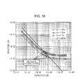
- FIG. 16 illustrates a relationship between the inductance L of the inductor 102 according to the peak frequency fe and the capacitance C of the capacitor 103.
- the horizontal axis indicates the value of C, and the vertical axis indicates the value of L.
- the values of L and C were plotted which were acquired from (Expression 1-3) where fe is 1.4*fm, 1.5*fm, and 2*fm. Plots are also illustrated when the product LC which of L and C is LmCm, that is, when the series resonance frequency fs is matched with fm.
- Lm indicates the self-inductance of the equivalent coil 301b
- Cm indicates the capacitance of the equivalent capacitor 301c.
- the point represents the optimum values of the inductance L and capacitance C where fs is matched with fm.
- fe is 1.4*fm
- L is 4.17 mH
- C is 3.12 nF.
- the condition for the peak frequency fe is preferably set to satisfy the relationship: fe ⁇ 2 * fd where the drive frequency of the vibration member 501 is fd.
- FIG. 13 illustrates the frequency characteristic of the alternating voltage Vo when the relationship fe ⁇ 2*fd is satisfied.
- 2*fd is the second harmonic frequency of the drive frequency fd.
- the waveform of the alternating voltage Vo is preferably be a SIN waveform having the second harmonic component and/or third harmonic component as small as possible. Because the drive waveform of the alternating voltage Vo in a real device is adjusted to have a pulse duty of 10% to 50%, the third harmonic component may particularly be required to reduce.
- the peak frequency fe may be set to a lower value than 2*fd to reduce the amplitude of the alternating voltage Vo of the frequency 2*fd of the third harmonic component lower than the drive frequency fd.
- the drive frequency fd is 46 kHz
- 2*fd is 92 kHz.
- the inductance L of the inductor 102 is set to 4 mH and the capacitance C of the capacitor 103 is set to 3.25 nF
- the peak frequency fe is 61.3 kHz, which may satisfy the condition.
- a second embodiment will be described next.
- This embodiment is different from the first embodiment in that a transformer is used to voltage boost.
- the configuration of a dust removing device which is the vibration member and the vibration modes are the same as those of the first embodiment, and a driving circuit will only be described below.
- FIG. 17A illustrates a driving circuit for a dust removing device according to the second embodiment.
- a secondary coil 401b of a transformer 401 is connected to a piezoelectric element 101 in parallel.
- a capacitor 103 is serially connected to a transformer primary coil 401a of the transformer 401.
- the capacitor 103 may be a capacitance element such as a film capacitor. Weakening the coupling of the transformer 401 allows the use of a leakage inductance of the transformer primary coil 401a and a leakage inductance of the transformer secondary coil 401b as an inductor.
- FIG. 17A equivalently illustrates the leakage inductances as the inductors 102a (leakage inductance of the transformer primary coil 401a) and 102b (leakage inductance of the transformer secondary coil 401b).
- the two leakage inductances and the capacitor 103 form series resonance.
- the capacitor 103 is connected to the lower side of the transformer primary coil 401a in FIG. 17A , it may be connected to the upper side (between the inductor 102a and the transformer primary coil 401a).
- the series resonance frequency by the leakage inductance 102a on the primary side, the leakage inductance 102b on the secondary side and the capacitor 103 is defined as fs, and the resonance frequency of the vibration member 501 is defined as fm may be expressed by Expressions 2-1 and 2-2.
- the leakage inductance 102a of the transformer primary coil 401a is L1
- the leakage inductance 102b of the transformer secondary coil 401b is L2
- the turns ratio of the secondary coil 401b to the primary coil 401a is N
- the capacitor 103 is C.
- Lm and Cm are equivalent circuit constants of mechanical vibrations of the piezoelectric element 101.
- Lm is a self-inductance of the equivalent coil 301b
- Cm is a capacitance of the equivalent capacitor 301c.
- a gentle frequency characteristic of the alternating voltage Vo may be acquired near fm by setting fs to a value close to fm in the following range: 0.73 * fm ⁇ fs ⁇ 1.2 * fm
- the coefficient relating to LC in the computation expression of fs is different between the primary side and the secondary side of the transformer to which the inductor 102 and capacitor 103 are connected.
- the configurations may roughly be divided into the following four types.
- the coefficient relating to LC is 1.
- the coefficient is N2*LC in (3). This is because L on the primary side corresponds to the square of the turns ratio N of the transformer when it is converted to the secondary side.
- the coefficient is (1/N2)*LC in (4). This is because C of the primary side corresponds to one square of the turns ratio N if it is converted to the secondary side.
- How to determine the values of the inductor 102 and capacitor 103 is the same as that of the first embodiment. In other words, by determining the peak frequency fe of the alternating voltage Vo first, one combination may be acquired.
- the peak frequency fe is set to satisfy the relationship: fe ⁇ 2 * fd where the drive frequency of the vibration member 501 is fd, like the first embodiment.
- FIG. 17B illustrates a first variation example of the driving circuit for the dust removing device in the second embodiment.
- the secondary coil 401b of the transformer 401 is connected to the piezoelectric element 101 in parallel, and the inductor 102 and capacitor 103 are serially connected to the transformer primary coil 401a.
- Other configurations excluding the one illustrated in FIG. 17B may be implemented if the inductor 102 and the capacitor 103 are serially connected to the transformer primary coil 401a.
- the inductor 102 may be connected to the primary side of the transformer 401 so that an element with an inductance value as small as 1/N 2 may be used, compared with the case connected to the secondary side. In this case, N is a turns ratio.
- the capacitor 103 may be connected to the primary side of the transformer 401 so that an element with a withstand voltage of 1/N may be used, compared with the case connected to the secondary side.
- the fs may be substantially matched with the resonance frequency fm of the vibration member 501.
- FIG. 17C illustrates a second variation example of the driving circuit for the dust removing device in the second embodiment.
- the secondary coil 401b of the transformer 401 is connected to the piezoelectric element 101 in parallel, and the capacitor 103 is serially connected to the transformer primary coil 401a, and the inductor 102 is serially connected to the transformer secondary coil 401b.
- the inductor 102 may be connected to the secondary side of the transformer 401 so that an element with a current acceptable value as small as 1/N may be used, compared with the case connected to the primary side.
- N is a turns ratio.
- the fs may be substantially matched with the resonance frequency fm of the vibration member 501.
- FIG. 17D illustrates a third variation example of the driving circuit for the dust removing device in the second embodiment.
- the secondary coil 401b of the transformer 401 is connected to the piezoelectric element 101 in parallel
- the inductor 102 is serially connected to the transformer primary coil 401a
- the capacitor 103 is serially connected to the transformer secondary coil 401b.
- the inductor 102 may be connected to the primary side of the transformer 401 so that an element with an inductance as small as 1/N 2 may be used, compared with the case connected to the secondary side.
- the capacitor 103 may be connected to the secondary side of the transformer 401 so that an element with a capacitance of 1/N 2 may be used, compared with the case connected to the primary side.
- the fs may be substantially matched with the resonance frequency fm of the vibration member 501.
- FIG. 17E illustrates a fourth variation example of the driving circuit for the dust removing device in the second embodiment.
- the secondary coil 401b of the transformer 401 is connected to the piezoelectric element 101 in parallel, and the inductor 102 and capacitor 103 are serially connected to the transformer secondary coil 401b.
- the inductor 102 may be connected to the secondary side of the transformer 401 so that an element with a current acceptable value as small as 1/N may be used, compared with the case connected to the primary side.
- the capacitor 103 may be connected to the secondary side of the transformer 401 so that an element with a capacitance of 1/N 2 may be used, compared with the case connected to the primary side.
- the fs may be matched with the resonance frequency fm of the piezoelectric element 101.
- a third embodiment will be described next.
- This embodiment is different from the first embodiment in that two vibration mode are alternately excited in the vibration member 501.
- the configurations of the vibration member 501 and driving circuit are the same as those of the first and second embodiment.
- the settings of frequency information and phase information in an instruction unit in a control apparatus are different from the first and second embodiment so that the vibrations to be excited may be standing-wave vibrations.
- FIG. 18A is a graph illustrating frequency of alternating voltages to be applied to a piezoelectric element and amplitudes of vibrations occurring in the piezoelectric element.
- f(m) is a resonance frequency of m-order out-of-plane bending vibrations
- f(m + 1) is a resonance frequency of out-of-plane bending vibrations of (m + 1)-order.
- f(m) is an order 10 out-of-plane bending vibration mode (first vibration mode) to be excited by opposite phase driving
- f(m + 1) is an order 11 out-of-plane bending vibration mode (second vibration mode) to be excited by same phase driving.
- the standing waves of the two vibration modes are alternately excited to remove dust adhered to a surface of an optical member which is an elastic body.
- the order 10 out-of-plane bending vibration is a first vibration mode(waveform A (solid line)), and the order 11 out-of-plane bending vibration is the second vibration mode (waveform B (broken line)) also in this embodiment.
- the first vibration mode A and second vibration mode B are out-of-plane bending vibration modes which bending deforms the vibration member 501 in the thickness direction of the optical member 502.
- the deformed shape in the first vibration mode A has opposite phases (with a phase difference of 180°) at left and right ends.
- the deformed shape in the second vibration mode B is in phase between the left and right ends (with a phase difference of 0°).
- the first vibration mode A is only excited under a resonance state. If the phase difference is set to 0° on the other hand, the second vibration mode B is excited.
- FIG. 18B illustrates examples of alternating voltages to be applied to piezoelectric elements for alternately exciting two standing-wave vibrations of different orders.
- the control apparatus may be the one illustrated in FIG. 4 .
- the alternating voltage Vo 1 is a voltage waveform to be applied to the piezoelectric element 101a
- the alternating voltage Vo 2 is a voltage waveform to be applied to the piezoelectric element 101b.
- the vertical axis indicates voltage amplitude
- the horizontal axis indicates time.
- an alternating voltage having a frequency near the inherent frequency of the order 10 bending vibration mode of the vibration member 501 and having a phase difference of 180° is applied to the piezoelectric elements 101a and 101b (opposite phase driving).
- the application of the alternating voltages excites the order 10 bending vibration mode in the vibration member 501.
- an alternating voltage having a frequency near the inherent frequency of the order 11 bending vibration mode of the vibration member 501 and having a phase difference of 0° is applied to the piezoelectric elements 101a and 101b next (same phase driving).
- the application of the alternating voltages excites the order 11 bending vibration mode in the vibration member 501.
- the phase difference is regarded as 180° if the first vibration mode vibrations are dominant in the vibrations occurring in the vibration member 501.
- the phase difference is regarded as 0° if the second vibration mode vibrations are dominant in the vibrations occurring in the vibration member 501.
- the alternating voltages Vo 1 and Vo 2 for the driving may sweet gradually from a high frequency side to a low frequency side near the inherent frequency as illustrated in FIG. 18B .
- the frequency of alternating voltages near the inherent frequency in the vibration member 501 may provide a large amplitude even with small applied voltage, improving the efficiency.
- generating vibrations in the first vibration mode in the vibration member 501 may separate the dust adhered to the optical member 502 at an anti-nodal position of vibrations in the first vibration mode. More specifically, dust is separated from the optical member 502 when vibrations in the first vibration mode apply an acceleration which is equal to or higher than the adhesion of the dust adhered optical member 502 to the dust. Furthermore, generating vibrations in the second vibration mode in the vibration member 501 may separate the dust adhered to the optical member 502 near a node of vibrations in the first vibration mode. Standing waves of different orders are excited to prevent positions without an amplitude in the optical member 502 by causing nodes of the two standing waves at different positions.
- the alternating voltages may be applied to only one of the piezoelectric elements 101a and 101b to excite one standing wave of out-of-plane bending vibrations in the vibration member 501 of a dust removing device.
- the number of piezoelectric elements to be provided in the elastic body is not limited to two as described above but may be one. In this case, the frequencies of alternating voltages to be applied to the piezoelectric elements may be swept to drive, without setting phase differences.
- a vibration member driving circuit causes vibrations in a vibration member (501) at least including an electro-mechanical energy conversion element and an elastic body by applying alternating voltage to the electro-mechanical energy conversion element fixed to the elastic body.
- the vibration member driving circuit includes an inductor (102) and capacitor (103) serially connected to the electro-mechanical energy conversion element. 0.73*fm ⁇ fs ⁇ 1.2*fm is satisfied where fs is the series resonance frequency by the inductor (102) and the capacitor and fm is the resonance frequency of the vibration member.
Landscapes
- Physics & Mathematics (AREA)
- Engineering & Computer Science (AREA)
- General Physics & Mathematics (AREA)
- Optics & Photonics (AREA)
- Mechanical Engineering (AREA)
- Multimedia (AREA)
- Signal Processing (AREA)
- Power Engineering (AREA)
- Electromagnetism (AREA)
- Camera Bodies And Camera Details Or Accessories (AREA)
- Studio Devices (AREA)
- Apparatuses For Generation Of Mechanical Vibrations (AREA)
- General Electrical Machinery Utilizing Piezoelectricity, Electrostriction Or Magnetostriction (AREA)
- Cleaning In General (AREA)
Abstract

Description
- Embodiments of the present invention relate to vibration member driving circuits.
- In recent years, with improved resolutions of image pickup elements, dust adhered to an optical system in use have affected captured images in image pickup apparatuses as optical apparatuses. Particularly, the resolutions of image pickup elements to be used in video cameras and still cameras have significantly been improved. For that, when external dust and/or dust (powder) such as wear debris caused on an internal mechanical rubbing surface are adhered to an optical member such as an infrared cut filter and an optical low pass filter near an image pickup element, the powder may appear on captured images because of less blurred images on an image pickup element surface.
- An image pickup unit of a copy machine or facsimile machine as an optical apparatus scans a line sensor or scans a document placed closer to a line sensor to read a flat document. In this case, when dust adheres to a light beam launching area, the dust appears on a scanned image. One piece of dust may appear as a line image which continues in a document feeding direction and deteriorates the quality of the image in a reading unit of a facsimile machine which scans and reads a document or a reading unit of a copy machine which reads, that is, skims a document during transport from an automatic document feeder.
- Japanese Patent Laid-Open No.
2008-207170 FIG. 3 is a schematic diagram illustrating a configuration of a dust removing device disclosed in Japanese Patent Laid-Open No.2008-207170 vibration member 501 having anoptical member 502 is provided on a light entrance side of animage pickup element 503.Piezoelectric elements vibration member 501. Alternating voltages having an equal frequency and a phase difference of 90° are applied to thepiezoelectric elements - The frequency of the alternating voltage to be applied is between a resonance frequency in an m-order (where m is a natural number) vibration mode which bends out of plane along the longitudinal direction of the
vibration member 501 and a resonance frequency in an (m + 1)-order vibration mode. In thevibration member 501, vibrations in the m-order vibration mode with a response with a resonance phenomenon and vibrations in the (m + 1)-order vibration mode with a 90° time phase difference (phase advanced by 90° from the m-order out-of-plane bending vibration) are excited with an equal amplitude and at equal vibration periods. Then, in thevibration member 501, synthesized vibrations (free-traveling waves) are generated in which the vibrations in two vibration modes are synthesized. The synthesized vibrations move the dust on the surface of thevibration member 501 in a desirable direction. - However, in a dust removing device in the past, the amplitude change of alternating voltage to be applied to the
piezoelectric element 101, that is, the gradient of a frequency characteristic of the alternating voltage may increase near the resonance frequency of thevibration member 501 in some frequency band to be used. For that reason, the alternating voltage largely changes when the resonance frequency of thevibration member 501 varies because of individual differences or the heat while the device is being driven changes the resonance frequency. The alternating voltage increased more than necessary may increase the power consumption because of a current increase or damage theoptical member 501 because of the increase of the vibration amplitude excited in thevibration member 501. When the alternating voltage is lower than necessary voltage, a sufficient vibration amplitude of the out-of-plane bending vibration to be excited in thevibration member 501 may not be acquired, and the dust removal efficiency may decrease. - One disclosed aspect of the embodiments provides a driving circuit which outputs a stable voltage amplitude in a used frequency band with a small change in alternating voltage to be applied to an electro-mechanical energy conversion element even when the resonance frequency of a vibration member varies or changes during the device is being driven.
- One embodiment in its first aspect provides a vibration member driving circuit as specified in
claim 1. - According to one disclosed aspect of the embodiments, a driving circuit may be provided which outputs a stable voltage amplitude in a used frequency band with a small change in alternating voltage to be applied to an electro-mechanical energy conversion element even when the resonance frequency of a vibration member varies or changes during the device is being driven.
- Further features of the embodiments will become apparent from the following description of exemplary embodiments with reference to the attached drawings.
-
FIGs. 1A to 1C illustrate a vibration member driving circuit according to a first embodiment. -
FIGs. 2A and 2B are perspective view of an image pickup apparatus to which one embodiment is applicable. -
FIG. 3 is a perspective view illustrating a structure of an image pickup unit of a camera body having a dust removing device. -
FIG. 4 illustrates a control apparatus for the dust removing device to which one embodiment is applicable. -
FIG. 5 illustrates a configuration of a driving circuit in the past. -
FIGs. 6A and 6B are graphs illustrating the frequencies of alternating voltages applied to piezoelectric elements, the amplitude of vibrations occurring in the piezoelectric elements, and their waveforms according to the first embodiment. -
FIG. 7 illustrates the displacement oforder 10 out-of-plane bending vibrations and the displacement oforder 11 out-of-plane bending vibrations which are excited in the vibration member and bend out of plane along the longitudinal direction and illustrating the arrangement of the piezoelectric elements. -
FIG. 8 illustrates a frequency characteristic of the voltage amplitude of the alternating voltage Vo when a driving circuit in the past is used. -
FIGs. 9A and 9B illustrate a simulation result describing frequency characteristics of a current amplitude and alternating voltages Vo when the series resonance frequency fs with the inductor and capacitor is substantially matched with the resonance frequency fm of the vibration member. -
FIGs. 10A and 10B illustrate results of simulations by calculations of how the alternating voltages Vo change in accordance with the changes in admittance. -
FIGs. 11A and 11B illustrate simulation results of how the alternating voltage Vo changes in accordance with the variations in the inductor, capacitor and the inherent capacitance of the piezoelectric element. -
FIG. 12 illustrates results of measurement of changes in power supply current against driving time. -
FIG. 13 illustrates the frequency characteristic of the alternating voltage Vo when the relationship fe < 2*fd is satisfied. -
FIGs. 14A and 14B illustrate simulation results describing changes in phase and alternating voltage Vo, compared with the past, in accordance with changes in fs/fm. -
FIG. 15 illustrates simulation results of the proportion of the amounts of changes in phase to the configuration of the example in the past in accordance with changes in fs/fm. -
FIG. 16 illustrates a relationship between the inductance L of the inductor according to the peak frequency fe and the capacitance C of the capacitor. -
FIGs. 17A to 17E illustrate driving circuits for a dust removing device having a transformer according to a second embodiment. -
FIGs. 18A and 18B are graphs illustrating frequency of alternating voltages to be applied to a piezoelectric element driven by standing waves, amplitudes of vibrations occurring in the piezoelectric element and voltage waveforms according to a third embodiments. - Embodiments of a vibration member driving circuit to which the present invention is applicable will be described with reference to drawings. A vibration member driving circuit of one embodiment may drive an object such as powder by vibrating a vibration member. One embodiment is applicable if a vibration member is vibrated to drive an object such as powder on the vibration member though a dust removing device for removing dust which is powder and a driving circuit therefor will be described according to embodiments below. According to the embodiments, powder refers to an 1 µm or larger to 100 µm or smaller object.
- Apparatuses having a vibration member and/or a driving circuit therefor of the embodiments may include optical apparatuses such as a camera (image pickup device), a facsimile machine, a scanner, a projector, a copy machine, and a printer. A vibration member and/or a driving circuit therefor of the embodiments are provided in an image pickup apparatus in embodiments below, for example. According to one disclosed aspect of the embodiments, an image pickup element such as a CCD and a CMOS sensor or a line sensor used in a copier or a facsimile machine, which is a photoelectric conversion element, is called a light receiving element.
- According to a first embodiment, a dust removing device which excites traveling waves in a vibration member to move dust which is powder is mounted in a camera.
-
FIG. 2A is a front perspective view, from the subject side, of a digital single-lens reflex camera which is an image pickup apparatus according to the first embodiment and illustrates a state without an imaging lens.FIG. 2B is a back perspective view of the camera from a photographer. Within acamera body 201, amirror box 202 is provided to which a imaging luminous flux passed through an imaging lens, not illustrated, is guided. A main mirror (quick return mirror) 203 is provided within themirror box 202. An image pickup unit having the dust removing device is provided on an imaging optical axis passed through the imaging lens, not illustrated. Themain mirror 203 may be held at an angle of 45° about an imaging optical axis so that a photographer may observe a subject image through afinder eye window 204 or may be held at a position avoiding an imaging luminous flux for guiding toward the image pickup element. A cleaninginstruction switch 205 is provided on the back of the camera and may be used for driving a vibration member which is the dust removing device. If a photographer presses the cleaninginstruction switch 205, an instruction unit 604 (refer toFIG. 4 ) is instructed to drive the dust removing device. -
FIG. 3 is a perspective view illustrating a structure of an image pickup unit of thecamera body 201 having a dust removing device that is a vibration member. Animage pickup element 503 is provided in the image pickup unit of thecamera body 201. Theimage pickup element 503 is a light receiving element such as a CCD and a CMOS sensor which converts a received subject image to an electric signal. Avibration member 501 is attached so as to tightly seal the space on the front surface of theimage pickup element 503. Thevibration member 501 at least includes a rectangular planeroptical member 502 which is an elastic body and a pair ofpiezoelectric element 101a (first electro-mechanical energy conversion element) and apiezoelectric element 101b (second electro-mechanical energy conversion element) which are electro-mechanical energy conversion elements adhered to both ends of theoptical member 502. Theoptical member 502 is an optical member with a high transmittance such as a cover glass, infrared cut filter, or an optical low pass filter. Light passing through theoptical member 502 enters to theimage pickup element 503. - The dimension in the thickness direction (vertical direction in the drawing) of the
piezoelectric elements optical member 502 is equal to the dimension in the thickness direction (vertical direction in the drawing) of theoptical member 502 so as to increase the generative force of the bending deformation against vibrations. Thepiezoelectric elements piezoelectric elements 101 when no distinction is particularly required. -
FIG. 4 illustrates a control apparatus for the dust removing device. The control apparatus includes theinstruction unit 604,pulse generating circuits circuits power supply circuit 605, and drivingcircuits instruction unit 604, frequency information, phase information, and pulse width information which are parameters of an alternating voltage signal, are transmitted to thepulse generating circuits vibration member 501, and equal frequencies are set to thepulse generating circuits FIG. 7 . Different values of phases from each other are input to thepulse generating circuits pulse generating circuits - The digital alternating voltage signal output from the pulse generating circuit 603 is input to the
switching circuits power supply circuit 605. The power supply circuit may be a general DC power supply circuit, DC-DC converter circuit or the like. The switching circuit may be a general H-bridge circuit. - The alternating voltage Vi is input to the driving
circuits piezoelectric elements vibration member 501. The synthesized vibrations become traveling waves and may move dust on the surface of theoptical member 502 in a desirable direction. The configuration of the drivingcircuits FIG. 1 . - The digital alternating voltage signal output from the pulse generating circuit 603 is input to the
switching circuits power supply circuit 605. The power supply circuit may be a general DC power supply circuit, DC-DC converter circuit or the like. The switching circuit may be a general H bridge circuit. - The alternating voltage Vi is input to the driving
circuits piezoelectric elements vibration member 501. The synthesized vibrations become traveling waves and may move dust on the surface of theoptical member 502 in a desirable direction. - Setting of the drive frequency will be described next.
FIG. 6A is a graph illustrating the frequencies of alternating voltages applied to thepiezoelectric elements 101 and the amplitude of vibrations occurring in thepiezoelectric elements 101. InFIG. 6A , f(m) is a resonance frequency of m-order out-of-plane bending vibrations, and f(m + 1) is a resonance frequency of (m + 1)-order out-of-plane bending vibrations. If a frequency fd of alternating voltage to be applied to thepiezoelectric element 101 is set to f(m) < fd < f(m + 1), vibrations at the frequency fd are acquired with an amplitude extended by the resonance phenomenon of the m-order out-of-plane bending vibrations and (m + 1)-order out-of-plane bending vibrations. The time periods of the vibrations are equal. On the other hand, as the frequency fd of the alternating voltage to be applied to thepiezoelectric element 101 is set lower than f(m), the amplitude of the (m + 1)-order out-of-plane bending vibrations is lower. As the frequency fd is set higher than f(m + 1), the amplitude of the m-order out-of-plane bending vibrations is lower. -
FIG. 7 is a schematic diagram illustrating the displacement oforder 10 out-of-plane bending vibrations and the displacement oforder 11 out-of-plane bending vibrations which are excited in thevibration member 501 and bend out of plane along the longitudinal direction and illustrating the arrangement of thepiezoelectric elements vibration member 501. The vertical axis indicates the out-of-plane vibration displacement. InFIG. 7 , theorder 10 out-of-plane bending vibration is indicated by a waveform A (solid line) as a first vibration mode, and theorder 11 out-of-plane bending vibration is indicated by a waveform B (broken line) as a second vibration mode. The first vibration mode A and second vibration mode B are an out-of-plane bending vibration mode, which bending deforms thevibration member 501 in the thickness direction of theoptical member 502. - When the driving
circuits piezoelectric elements vibration member 501 and are superposed. According to this embodiment, the vibration modes minimum required for removing dust are theorder 10 bending vibration mode as the first vibration mode and theorder 11 bending vibration mode as the second vibration mode. However, the vibration modes are not limited thereto. The optical effective area corresponding to theimage pickup element 503 is the range illustrated inFIG. 7 . The deformed shape in the first vibration mode A has opposite phases (with a phase difference of 180°) at left and right ends. On the other hand, the deformed shape in the second vibration mode B is in phase between the left and right ends (with a phase difference of 0°). In other words, if the phase difference between alternating voltages to be applied to thepiezoelectric element 101a andpiezoelectric element 101b is set to 180°, the first vibration mode A only occurs. If the phase difference is set to 0° on the other hand, the second vibration mode B only occurs. Thus, if the phase difference is set to 90°, the first vibration mode A and second vibration mode B may be caused simultaneously, and the traveling waves from the synthesized vibrations may occur in the right direction ofFIG. 7 . -
FIG. 6B illustrates examples of alternating voltages to be applied to the piezoelectric elements for simultaneously exciting vibration modes of different orders. The alternatingvoltage Vo 1 is a voltage waveform to be applied to thepiezoelectric element 101a, and the alternatingvoltage Vo 2 is a voltage waveform to be applied to thepiezoelectric element 101b. The vertical axis indicates voltage amplitude, and the horizontal axis indicates time. The frequency of the alternatingvoltages Vo 1 andVo 2 is constant at fd described above, and the phase difference between the alternating voltages is 90°. However, the alternatingvoltages Vo 1 andVo 2 may only be required to have different phases, and the phase difference is not limited to 90°. - In the dust removing device, the dust adhered to the surface of the
optical member 502 moves as if it bounces off under the force in the normal direction of the surface of theoptical member 502 when theoptical member 502 pushes up the dust out of plane. In other words, when the speed of the synthesized vibration displacement of thevibration member 501 in phases of a drive frequency period is positive, the dust is pushed up out of plane, and the dust moves under the force in the normal direction of the synthesized vibration displacement in the phase. Referring toFIG. 7 , by repeatedly applying vibrations to the dust adhered to the surface of the effective area of theoptical member 502, the dust may be moved and removed in the right direction ofFIG. 7 . - With reference to
FIGs. 1A to 1C , a driving circuit of the first embodiment will be described.FIG. 1A illustrates a driving circuit for the dust removing device according to the first embodiment. The driving circuit includes aninductor 102 and acapacitor 103 which are serially connected to thepiezoelectric element 101. Though thecapacitor 103 is connected to the lower side of thepiezoelectric element 101 inFIG. 1 , it may be connected to the upper side (between theinductor 102 and the piezoelectric element 101). As illustrated inFIG. 1C , aresistance 104 may be connected in parallel with thepiezoelectric element 101. Theresistance 104 may be set to 1 MΩ with which current hardly flows to prevent power consumption in the resistance part. Providing theresistance 104 may define the potential at the connection point between thecapacitor 103 and thepiezoelectric element 101, stable alternating voltages may be applied across the piezoelectric elements. - The
inductor 102 may be an inductance element such as a coil. Thecapacitor 103 may be a capacitance element such as a film capacitor. One disclosed aspect of the embodiments is characterized in that the series resonance frequency of theinductor 102 and thecapacitor 103 is substantially matched with the resonance frequency of the vibration member 501 (set within a tolerance, which will be described below). - An equivalent circuit of the
piezoelectric element 101 will be described with reference toFIG. 1B. FIG. 1B illustrates an equivalent circuit of thepiezoelectric element 101. The equivalent circuit of thepiezoelectric element 101 includes an RLC series circuits (equivalent coil 301b of self-inductance Lm,equivalent capacitor 301c of capacitance Cm, andequivalent resistance 301d of resistance value Rm) of the mechanical vibration part of thevibration member 501 and acapacitor 301a functioning as inherent capacitance Cd of thepiezoelectric element 101 connected to the RLC series circuit in parallel. - According to the embodiments, the series resonance frequency by the
inductor 102 andcapacitor 103 is defined as fs, and the resonance frequency of thevibration member 501 is defined as fm. When the self-inductance of theinductor 102 is L and the capacitance of thecapacitor 103 is C,

- The substantially matched fs and fm allows a gentle frequency characteristic of the alternating voltage Vo near fm.
- With reference to
FIG. 5 , there will be described a configuration of a driving circuit in the past in which theinductor 102 is only connected to thepiezoelectric element 101 in series. As illustrated inFIG. 5 , serially connecting theinductor 102 to thepiezoelectric element 101 may form an LC series resonance circuit by the inherent capacitance of thepiezoelectric element 101 and theinductor 102. The voltage amplitude of the alternating voltage Vi is boosted to a desirable voltage by the LC series resonance circuit, and the alternating voltage Vo is output. -
FIG. 8 illustrates a frequency characteristic of the voltage amplitude of the alternating voltage Vo when a driving circuit in the past is used. The horizontal axis indicates frequency, and the vertical axis indicates voltage amplitude. The plots indicate a characteristic caused when the value of theinductor 102 is changed from 40 µH to 90 µH. InFIG. 8 , f(m) is a resonance frequency of an m-order out-of-plane bending vibrations, and f(m + 1) is a resonance frequency of an (m + 1)-order out-of-plane bending vibrations. The frequency fd of the alternating voltage Vo to be applied to thepiezoelectric element 101 is set to f(m) < fd < f(m + 1).FIG. 8 illustrates that the amplitude change of the alternating voltage Vo occurs near fm and f(m + 1). As the value of theinductor 102 increases, the change in voltage amplitude increases near fm, f(m + 1) and fd. As the value of theinductor 102 decreases, the change in voltage amplitude decreases. However, a desirable voltage amplitude may not be acquired because of the decreasing voltage boost rate. As the value of theinductor 102 decreases, the electric resonance frequency fe of the LC series circuit shifts to a higher frequency. Thus, the harmonics component of the drive frequency fd is superposed over the fundamental harmonic, distorting the waveform. A large waveform distortion may excite unnecessary vibrations in thevibration member 501. - Like the example in the past, the reason why the amplitude change of the alternating voltage Vo occurs near fm or f(m + 1) is because the self-inductance Lm and capacitance Cm of the mechanical vibration part of the
vibration member 501 cause a change in impedance. On the other hand, according to the embodiments, fs and fm are substantially matched for impedance matching in the mechanical vibration part of thevibration member 501. As a result, the amplitude change of the alternating voltage Vo may be reduced. Moreover, the gentle frequency characteristic of the alternating voltage Vo near fm may reduce the change in admittance (equivalent resistance 301d) and/or the change in alternating voltage Vo due to the variations ininductor 102 andcapacitor 103. Because of the impedance matching of the mechanical vibration part of thevibration member 501, the frequency characteristic is hardly influenced by variations of elements near fm. -
FIGs. 9A and 9B illustrate simulation results describing frequency characteristics of the alternating voltages Vo when the series resonance frequency fs with theinductor 102 andcapacitor 103 is substantially matched with the resonance frequency fm of thevibration member 501. According to this embodiment, the driving circuit has the configuration inFIG. 1A . Thevibration member 501 of this embodiment has two out-of-plane bending vibrations, and the resonance frequencies fm include two of f(m) and f(m + 1). According to this embodiment, the series resonance frequency fs is set to fs = 0.83*f(m) in accordance with the resonance frequency f(m). Ideally, fs and fm are completely matched. However, fs is set to a lower value than fm because raising the voltage boost rate of the voltage amplitude is difficult. On the basis of calculations, when fs is lower than fm, the voltage boost rate tends to increase. When fs is higher than fm, the voltage boost rate tends to decrease.
Though the series resonance frequency fs is matched with f(m), the desirable effect may be acquired when it is a frequency near f(m + 1). - In this simulation, the self-inductance Lm of the
equivalent coil 301b was set to 0.04 H, and the capacitance Cm of theequivalent capacitor 301c was set to 44 pF. f(m) was set to 120 kHz, and f(m + 1) was set to 128 kHz, and the drive frequency fd was set to 123 kHz. The self-inductance L of theinductor 102 was set to 82 µH, and the capacitance C of thecapacitor 103 was set to 31 nF (fs = 0.83*fm). Plots with theinductor 102 set to 68 µH and thecapacitor 103 set to 42 n (fs=0.79*fm) are also illustrated though they are overlapped. An example in the past is also illustrated as a comparison example in which theinductor 102 was set to 68 µH when the configuration of the driving circuit inFIG. 5 is used. (Stabilizing Voltage) -
FIG. 9A illustrates a frequency characteristic of the current amplitude to be fed to the driving circuit.FIG. 9B illustrates a frequency characteristic of the voltage amplitude of the alternating voltage Vo. As illustrated inFIGs. 9A and 9B , substantially matching between fs and fm may provide a gentle frequency characteristic of the alternating voltage Vo near f(m) and f(m + 1). In other words, stable voltage is applied to a change in resonance frequency of thevibration member 501, which may reduce changes in drive current. For example, when the resonance frequency f(m + 1) decreases over time during driving, the amplitude of the alternating voltage increases and the drive current increases in the example in the past. According to one embodiment, the changes may be reduced. - The electric resonance by the
inductor 102 and thecapacitor 301a which is an inherent capacitance of thecapacitor 103 andpiezoelectric element 101 may be used to set the amplitude of the alternating voltage Vo to have a peak at a certain frequency. Defining the peak frequency of the alternating voltage Vo as fe and setting fe to a higher frequency than fm may provide a frequency characteristic with less voltage change even when the drive frequency fd of thevibration member 501 is changed in the frequency band from fm to fe. According to this embodiment, all of the peak frequencies fe were set to the range from 180 to 200 kHz. -
FIGs. 10A and 10B illustrate the effects of reduction of changes of the alternating voltage Vo.FIGs. 10A and 10B illustrate the results of simulations by calculations of how the alternating voltage Vo changes in accordance with the changes in admittance. The changes in admittance were calculated by changing the value of theequivalent resistance 301d from 10% to 100% of a reference value. As the equivalent resistance decreases, the admittance increases.FIG. 10A illustrates an example in the past, andFIG. 10B illustrates this embodiment.FIGs. 10A and 10B illustrate that this embodiment reduced the influence of a change in admittance to about 20% of that of the example in the past. -
FIGs. 11A and 11B illustrate simulation results of how the alternating voltage Vo changes in accordance with the variations in theinductor 102,capacitor 103 and the inherent capacitance of thepiezoelectric element 101. Random number calculation was performed on a uniform distribution by Monte Carlo method when the variation of the self-inductance L of theinductor 102 is ± 20%, the variation of the capacitance C of thecapacitor 103 is ± 10%, and the variation of thecapacitor 301a which is the inherent capacitance Cd of thepiezoelectric element 101 is ± 10%.FIG. 11A illustrates an example in the past, andFIG. 11B illustrates this embodiment. According to this embodiment, the influence of the variations of elements of the entire driving circuit including thepiezoelectric element 101 is reduced to about 70% of that of the example in the past. - The
vibration member 501 was actually driven by the driving circuit of this embodiment, and power supply currents are compared.FIG. 12 illustrates results of measurement of changes in power supply current against driving time. The power supply used was 12 VDC power supply. In a driving circuit of the example in the past, the power supply current increased about twice as the initial value after 20 seconds. In the driving circuit of this embodiment, the increase was about 40%. Thus, the power consumption may be reduced. - Next, there will be described the acceptable range of the relationship between the series resonance frequency fs by the
inductor 102 andcapacitor 103 serially connected to thepiezoelectric element 101 and the resonance frequency fm of the vibration member 501 (the range of substantial match between fs and fm). According to this embodiment, fm and fs are completely matched. However, the embodiments are not limited to the case where fs and fm are completely matched. In other words, fs and fm may be set to close values within a certain range for a gentle frequency characteristic of the alternating voltage Vo near fm. However, as the difference between fs and fm decreases, the effect increases. - According to the embodiments, in order to acquire the effective range of fs, the phase changes of the alternating voltage Vo near the resonance frequency fm of the
piezoelectric element 101 were focused.FIG. 14A illustrates simulation results illustrating phases of the alternating voltage Vo. The horizontal axis indicates frequency.FIG. 14A illustrates changes in phase of Vo from 40 kHz to 48 kHz where the resonance frequency fm is 44.142 kHz. In this simulation, the driving circuit ofFIG. 1A was used. The ratio of the series resonance frequency fs by theinductor 102 andcapacitor 103 to fm (fs/fm) were changed in the range from 0.73 to 1.2, and the changed ratios were plotted. - Here, values of L and C were adjusted such that the peak frequency fe may be 61.798 kHz (= 1.4*fm) at all times, and fs/fm was changed. The peak frequency fe was kept constant because the amplitude of Vo largely changes near the resonance frequency fm of the
vibration member 501 in accordance with the value of fe. For a comparison reference configuration in the past, the circuit inFIG. 5 was used for the calculation, and the calculation results were plotted. The self-inductance L of theinductor 102 in this case was 1.97 mH, and the peak frequency fe of the alternating voltage Vo was set to 61.798 kHz (= 1.4*fm). -
FIG. 14A illustrates that Vo of the configuration of the example in the past has a phase delayed by up to 60°. On the other hand, if fs/fm = 1, Vo hardly has phase changes. If fs/fm = 1, the self-inductance L of theinductor 102 is 4.17 mH, and the capacitance C of thecapacitor 103 is 3.12 nF. There is a tendency that the degree of satisfaction of fs/fm < 1 increases, the change of phase to the negative side increases. As the degree of satisfaction of fs/fm > 1 increases, the change of phase to the positive side increases. -
FIG. 14B illustrates the results of simulations describing the changes in alternating voltages Vo according to frequencies in order to check the relationship between phase changes of the alternating voltage Vo inFIG. 14A and the amplitude changes of the alternating voltage Vo. The simulation conditions are the same as those ofFIG. 14A , and simulation results with fs/fm changed in the range from 0.73 to 1.2 and a configuration of the example in the past were compared and were plotted. The tendencies of the amounts of changes in phase illustrated inFIG. 14B and the amounts of changes in voltage illustrated inFIG. 14A correspond. In other words, as the change in phase of Vo increases, the change in amplitude of Vo increases. -
FIG. 15 illustrates simulation results of the proportion of the amounts of changes in phase to the configuration of the example in the past in accordance with changes in fs/fm. The horizontal axis indicates fs/fm which is the ratio of fs to the resonance frequency fm of thevibration member 501. The vertical axis indicates the proportion of the amounts of changes in phase to the configuration of the example in the past and was calculates as follows. First, the absolute values of the amounts of changes in phase of Vo when the configuration of the example in the past was used in the range from 40 kHz to 48 kHz, and the maximum value was detected. This will be called "the maximum amount of change in phase of the configuration in the past". Next, on the basis of the configuration inFIG. 1A , the absolute values of the amounts of change in phase of Vo were calculated in the range from 40 kHz to 48 kHz by using fs/fm as a parameter, and the maximum value was detected. This will be called "the maximum amount of change according to fs/fm". The proportion of the amount of change in phase to the configuration of the example in the past may be expressed with a vertical axis acquired by calculating the ratio therebetween as: - "the maximum amount of change according to fs/fm "/"the maximum amount of change in phase of the configuration in the past".
- According to the embodiments, as illustrated in
FIG. 15 , the condition that the proportion of the amount of change in phase is half of the configuration of the example in the past was defined as a threshold value, and the range was acquired where a gentle frequency characteristic of the alternating voltage Vo near fm may be acquired. As the result, the range where the effect of fs/fm may be acquired was:
The range was calculated where the peak frequency fe was 61.798 kHz (= 1.4*fm), the inherent capacitance Cd of thecapacitor 301a of thepiezoelectric element 101 was 3.5 nF. However, substantially equivalent calculate results may be acquired even when the values of the peak frequency fe and/ or inherent capacitance Cd are changed. The range was also calculated where the self-inductance Lm of theequivalent coil 301b in thepiezoelectric element 101 was 0.1 H, the capacitance Cm of theequivalent capacitor 301c was 130 pF, and the value of resistance Rm of theequivalent resistance 301d was 1 kΩ. - On the basis of the range, the amount of change in phase difference of the alternating voltages Vo may be reduced to the half or smaller so that the amount of change in Vo may substantially be reduced to the half or smaller, compared with the past. In other words, even without the complete match between fs and fm, the satisfaction of the aforementioned relationship between fs and fm may provide a gentler frequency characteristic of the alternating voltage Vo near fm than before.
- Next, how to determine the values of the
inductor 102 andcapacitor 103 will be described. Because the series resonance frequency fs depends on the product of the inductance L of theinductor 102 and the capacitance C of thecapacitor 103, many combinations may define the same fs. On the other hand, the peak frequency fe of the alternating voltage Vo may be determined first to acquire one combination. - The peak frequency fe of Vo may be calculated from the inductance L of the
inductor 102, the capacitance C of thecapacitor 103, and the inherent capacitance Cd of thepiezoelectric element 101. The peak frequency fe may be expressed by Expression 1-3:
- In order to calculate the actual peak frequency fe, the
piezoelectric element 101 is equivalently regarded as a capacitor, and Cd' in consideration of an influence of the RLC series circuit of the mechanical vibration part is used. For example, when the influence of the RLC series circuit of the mechanical vibration part corresponds to a capacity change of 44 pF,
may be used for the calculation. - The functions of L and C may be acquired by determining the value of fe from the expression of the peak frequency fe.
FIG. 16 illustrates a relationship between the inductance L of theinductor 102 according to the peak frequency fe and the capacitance C of thecapacitor 103. The horizontal axis indicates the value of C, and the vertical axis indicates the value of L. The values of L and C were plotted which were acquired from (Expression 1-3) where fe is 1.4*fm, 1.5*fm, and 2*fm. Plots are also illustrated when the product LC which of L and C is LmCm, that is, when the series resonance frequency fs is matched with fm. As described above, Lm indicates the self-inductance of theequivalent coil 301b, and Cm indicates the capacitance of theequivalent capacitor 301c. - Referring to
FIG. 16 , the functions of the inductor and capacitor when fe is fixed intersects with the function of LC = LmCm at one point. The point represents the optimum values of the inductance L and capacitance C where fs is matched with fm. For example, fe is 1.4*fm, L is 4.17 mH, and C is 3.12 nF. - Next, the value of fe will be described. According to the embodiments, the condition for the peak frequency fe is preferably set to satisfy the relationship:

where the drive frequency of thevibration member 501 is fd. -
FIG. 13 illustrates the frequency characteristic of the alternating voltage Vo when the relationship fe < 2*fd is satisfied. 2*fd is the second harmonic frequency of the drive frequency fd. The waveform of the alternating voltage Vo is preferably be a SIN waveform having the second harmonic component and/or third harmonic component as small as possible. Because the drive waveform of the alternating voltage Vo in a real device is adjusted to have a pulse duty of 10% to 50%, the third harmonic component may particularly be required to reduce. The peak frequency fe may be set to a lower value than 2*fd to reduce the amplitude of the alternating voltage Vo of thefrequency 2*fd of the third harmonic component lower than the drive frequency fd. For example, when the drive frequency fd is 46 kHz, 2*fd is 92 kHz. In this case, when the inductance L of theinductor 102 is set to 4 mH and the capacitance C of thecapacitor 103 is set to 3.25 nF, the peak frequency fe is 61.3 kHz, which may satisfy the condition. - A second embodiment will be described next. This embodiment is different from the first embodiment in that a transformer is used to voltage boost. The configuration of a dust removing device which is the vibration member and the vibration modes are the same as those of the first embodiment, and a driving circuit will only be described below.
-
FIG. 17A illustrates a driving circuit for a dust removing device according to the second embodiment. In the configuration of the driving circuit, asecondary coil 401b of atransformer 401 is connected to apiezoelectric element 101 in parallel. Acapacitor 103 is serially connected to a transformerprimary coil 401a of thetransformer 401. Thecapacitor 103 may be a capacitance element such as a film capacitor. Weakening the coupling of thetransformer 401 allows the use of a leakage inductance of the transformerprimary coil 401a and a leakage inductance of the transformersecondary coil 401b as an inductor. -
FIG. 17A equivalently illustrates the leakage inductances as the inductors 102a (leakage inductance of the transformerprimary coil 401a) and 102b (leakage inductance of the transformersecondary coil 401b). The two leakage inductances and thecapacitor 103 form series resonance. Though thecapacitor 103 is connected to the lower side of the transformerprimary coil 401a inFIG. 17A , it may be connected to the upper side (between theinductor 102a and the transformerprimary coil 401a). The series resonance frequency by theleakage inductance 102a on the primary side, theleakage inductance 102b on the secondary side and thecapacitor 103 is defined as fs, and the resonance frequency of thevibration member 501 is defined as fm may be expressed by Expressions 2-1 and 2-2.

where theleakage inductance 102a of the transformerprimary coil 401a is L1, theleakage inductance 102b of the transformersecondary coil 401b is L2, the turns ratio of thesecondary coil 401b to theprimary coil 401a is N, and thecapacitor 103 is C. - As described above, Lm and Cm are equivalent circuit constants of mechanical vibrations of the
piezoelectric element 101. Lm is a self-inductance of theequivalent coil 301b, and Cm is a capacitance of theequivalent capacitor 301c. - Like the first embodiment, without complete match between the series resonance frequency fs and the resonance frequency fm of the
vibration member 501, a gentle frequency characteristic of the alternating voltage Vo may be acquired near fm by setting fs to a value close to fm in the following range:
In configurations using a transformer, the coefficient relating to LC in the computation expression of fs is different between the primary side and the secondary side of the transformer to which theinductor 102 andcapacitor 103 are connected. The configurations may roughly be divided into the following four types. - (1) Configuration in which LC are connected to the primary side of the transformer
- (2) Configuration in which LC are connected to the secondary side of the transformer
- (3) Configuration in which L and C are connected to the primary side of the transformer and the secondary side of the transformer, respectively
- (4) Configuration in which C and L are connected to the primary side of the transformer and the secondary side of the transformer, respectively.
- In (1) and (2), the coefficient relating to LC is 1. On the other hand, the coefficient is N2*LC in (3). This is because L on the primary side corresponds to the square of the turns ratio N of the transformer when it is converted to the secondary side. The coefficient is (1/N2)*LC in (4). This is because C of the primary side corresponds to one square of the turns ratio N if it is converted to the secondary side. How to determine the values of the
inductor 102 andcapacitor 103 is the same as that of the first embodiment. In other words, by determining the peak frequency fe of the alternating voltage Vo first, one combination may be acquired. - The peak frequency fe is set to satisfy the relationship:

where the drive frequency of thevibration member 501 is fd, like the first embodiment. -
FIG. 17B illustrates a first variation example of the driving circuit for the dust removing device in the second embodiment. In the configuration of the driving circuit, thesecondary coil 401b of thetransformer 401 is connected to thepiezoelectric element 101 in parallel, and theinductor 102 andcapacitor 103 are serially connected to the transformerprimary coil 401a. Other configurations excluding the one illustrated inFIG. 17B may be implemented if theinductor 102 and thecapacitor 103 are serially connected to the transformerprimary coil 401a. Theinductor 102 may be connected to the primary side of thetransformer 401 so that an element with an inductance value as small as 1/N2 may be used, compared with the case connected to the secondary side. In this case, N is a turns ratio. Thecapacitor 103 may be connected to the primary side of thetransformer 401 so that an element with a withstand voltage of 1/N may be used, compared with the case connected to the secondary side. The series resonance frequency fs may be expressed by Expression 2-3:
which is the same as Expression 1-1 where the inductance of the
inductor 102 is L and the capacitance of thecapacitor 103 is C. - The fs may be substantially matched with the resonance frequency fm of the
vibration member 501. -
FIG. 17C illustrates a second variation example of the driving circuit for the dust removing device in the second embodiment. In the configuration of the driving circuit, thesecondary coil 401b of thetransformer 401 is connected to thepiezoelectric element 101 in parallel, and thecapacitor 103 is serially connected to the transformerprimary coil 401a, and theinductor 102 is serially connected to the transformersecondary coil 401b. Theinductor 102 may be connected to the secondary side of thetransformer 401 so that an element with a current acceptable value as small as 1/N may be used, compared with the case connected to the primary side. In this case, N is a turns ratio. The series resonance frequency fs may be expressed by Expression 2-4:
where the inductance of theinductor 102 is L and the capacitance of thecapacitor 103 is C. - The fs may be substantially matched with the resonance frequency fm of the
vibration member 501. -
FIG. 17D illustrates a third variation example of the driving circuit for the dust removing device in the second embodiment. In the configuration of the driving circuit, thesecondary coil 401b of thetransformer 401 is connected to thepiezoelectric element 101 in parallel, theinductor 102 is serially connected to the transformerprimary coil 401a, and thecapacitor 103 is serially connected to the transformersecondary coil 401b. Theinductor 102 may be connected to the primary side of thetransformer 401 so that an element with an inductance as small as 1/N2 may be used, compared with the case connected to the secondary side. Thecapacitor 103 may be connected to the secondary side of thetransformer 401 so that an element with a capacitance of 1/N2 may be used, compared with the case connected to the primary side. The series resonance frequency fs in this case may be expressed by Expression 2-5:
- The fs may be substantially matched with the resonance frequency fm of the
vibration member 501. -
FIG. 17E illustrates a fourth variation example of the driving circuit for the dust removing device in the second embodiment. In the configuration of the driving circuit, thesecondary coil 401b of thetransformer 401 is connected to thepiezoelectric element 101 in parallel, and theinductor 102 andcapacitor 103 are serially connected to the transformersecondary coil 401b. Theinductor 102 may be connected to the secondary side of thetransformer 401 so that an element with a current acceptable value as small as 1/N may be used, compared with the case connected to the primary side. Thecapacitor 103 may be connected to the secondary side of thetransformer 401 so that an element with a capacitance of 1/N2 may be used, compared with the case connected to the primary side. The series resonance frequency fs in this case may be expressed by Expression 2-6:
- The fs may be matched with the resonance frequency fm of the
piezoelectric element 101. - A third embodiment will be described next. This embodiment is different from the first embodiment in that two vibration mode are alternately excited in the
vibration member 501. The configurations of thevibration member 501 and driving circuit are the same as those of the first and second embodiment. The settings of frequency information and phase information in an instruction unit in a control apparatus are different from the first and second embodiment so that the vibrations to be excited may be standing-wave vibrations. -
FIG. 18A is a graph illustrating frequency of alternating voltages to be applied to a piezoelectric element and amplitudes of vibrations occurring in the piezoelectric element. In this case, f(m) is a resonance frequency of m-order out-of-plane bending vibrations, and f(m + 1) is a resonance frequency of out-of-plane bending vibrations of (m + 1)-order. InFIGs. 18A and 18B , f(m) is anorder 10 out-of-plane bending vibration mode (first vibration mode) to be excited by opposite phase driving, and f(m + 1) is anorder 11 out-of-plane bending vibration mode (second vibration mode) to be excited by same phase driving. According to this embodiment, the standing waves of the two vibration modes are alternately excited to remove dust adhered to a surface of an optical member which is an elastic body. - Describing according to the first embodiment with reference to
FIG. 7 , theorder 10 out-of-plane bending vibration is a first vibration mode(waveform A (solid line)), and theorder 11 out-of-plane bending vibration is the second vibration mode (waveform B (broken line)) also in this embodiment. The first vibration mode A and second vibration mode B are out-of-plane bending vibration modes which bending deforms thevibration member 501 in the thickness direction of theoptical member 502. The deformed shape in the first vibration mode A has opposite phases (with a phase difference of 180°) at left and right ends. On the other hand, the deformed shape in the second vibration mode B is in phase between the left and right ends (with a phase difference of 0°). In other words, if the phase difference between alternating voltages to be applied to thepiezoelectric element 101a andpiezoelectric element 101b is set to 180°, the first vibration mode A is only excited under a resonance state. If the phase difference is set to 0° on the other hand, the second vibration mode B is excited. -
FIG. 18B illustrates examples of alternating voltages to be applied to piezoelectric elements for alternately exciting two standing-wave vibrations of different orders. The control apparatus may be the one illustrated inFIG. 4 . The alternatingvoltage Vo 1 is a voltage waveform to be applied to thepiezoelectric element 101a, and the alternatingvoltage Vo 2 is a voltage waveform to be applied to thepiezoelectric element 101b. The vertical axis indicates voltage amplitude, and the horizontal axis indicates time. - In order to alternately generate vibrations of the two vibration modes, an alternating voltage having a frequency near the inherent frequency of the
order 10 bending vibration mode of thevibration member 501 and having a phase difference of 180° is applied to thepiezoelectric elements order 10 bending vibration mode in thevibration member 501. After exciting theorder 10 bending vibration mode for a predetermined period of time, an alternating voltage having a frequency near the inherent frequency of theorder 11 bending vibration mode of thevibration member 501 and having a phase difference of 0° is applied to thepiezoelectric elements order 11 bending vibration mode in thevibration member 501. - When the first vibration mode is to be excited but the phase difference between the alternating voltages shifts from 180° within the margin of error due to an influence such as element variations of the driving circuit, the phase difference is regarded as 180° if the first vibration mode vibrations are dominant in the vibrations occurring in the
vibration member 501. Similarly, when the second vibration mode is to be excited but the phase difference between the alternating voltages shifts from 0° within the margin of error due to an influence such as element variations of the driving circuit, the phase difference is regarded as 0° if the second vibration mode vibrations are dominant in the vibrations occurring in thevibration member 501. - Repeating this driving (opposite phase driving and same phase driving) my alternately excite vibrations in the
order 10 andorder 11 out-of-plane bending vibration mode. The alternatingvoltages Vo 1 andVo 2 for the driving may sweet gradually from a high frequency side to a low frequency side near the inherent frequency as illustrated inFIG. 18B . The frequency of alternating voltages near the inherent frequency in thevibration member 501 may provide a large amplitude even with small applied voltage, improving the efficiency. - In this way, generating vibrations in the first vibration mode in the
vibration member 501 may separate the dust adhered to theoptical member 502 at an anti-nodal position of vibrations in the first vibration mode. More specifically, dust is separated from theoptical member 502 when vibrations in the first vibration mode apply an acceleration which is equal to or higher than the adhesion of the dust adheredoptical member 502 to the dust. Furthermore, generating vibrations in the second vibration mode in thevibration member 501 may separate the dust adhered to theoptical member 502 near a node of vibrations in the first vibration mode. Standing waves of different orders are excited to prevent positions without an amplitude in theoptical member 502 by causing nodes of the two standing waves at different positions. - The alternating voltages may be applied to only one of the
piezoelectric elements vibration member 501 of a dust removing device. Like this embodiment, when vibrations to be generated in vibration modes of different orders are shifted at intervals in time, the number of piezoelectric elements to be provided in the elastic body is not limited to two as described above but may be one. In this case, the frequencies of alternating voltages to be applied to the piezoelectric elements may be swept to drive, without setting phase differences. - While the embodiments have been described with reference to exemplary embodiments, it is to be understood that the invention is not limited to the disclosed exemplary embodiments. The scope of the following claims is to be accorded the broadest interpretation so as to encompass all such modifications and equivalent structures and functions.
A vibration member driving circuit causes vibrations in a vibration member (501) at least including an electro-mechanical energy conversion element and an elastic body by applying alternating voltage to the electro-mechanical energy conversion element fixed to the elastic body. The vibration member driving circuit includes an inductor (102) and capacitor (103) serially connected to the electro-mechanical energy conversion element. 0.73*fm < fs < 1.2*fm is satisfied where fs is the series resonance frequency by the inductor (102) and the capacitor and fm is the resonance frequency of the vibration member.
Claims (9)
- A vibration member driving circuit which causes vibrations in a vibration member (501) at least including an electro-mechanical energy conversion element and an elastic body by applying alternating voltage to the electro-mechanical energy conversion element fixed to the elastic body, the circuit comprising:an inductor (102) and a capacitor (103) serially connected to the electro-mechanical energy conversion element, wherein

is satisfied where fs is a series resonance frequency by the inductor (102) and the capacitor (103) and fm is a resonance frequency of the vibration member (501). - A vibration member driving circuit which causes vibrations in a vibration member at least including an electro-mechanical energy conversion element and an elastic body by applying alternating voltage to the electro-mechanical energy conversion element fixed to the elastic body, the circuit comprising:a transformer having a primary coil to which alternating voltages are applied and a secondary coil connected in parallel to the electro-mechanical energy conversion elements; andan inductor and capacitor serially connected to the electro-mechanical energy conversion element on at least one of the primary side and secondary side of the transformer, wherein

is satisfied where fs is a series resonance frequency by the inductor and the capacitor and fm is a resonance frequency of the vibration member. - The vibration member driving circuit according to Claim 2, wherein the inductor is a leakage inductance of the transformer.
- The vibration member driving circuit according to any one of Claims 1 to 3, wherein fe < 2*fd is satisfied where fe is a peak frequency of an alternating voltage to be applied to the electro-mechanical energy conversion element and fd is a drive frequency of the vibration member.
- The vibration member driving circuit according to any one of Claims 1 to 4, wherein the vibration member has an elastic body and a first electro-mechanical energy conversion element and second electro-mechanical energy conversion element fixed to the elastic body; and
alternating voltages with waveforms having a frequency which generates vibrations superposing vibrations in a first vibration mode and vibrations in a second vibration mode of different orders in the vibration member and different phases are applied to the first and second electro-mechanical energy conversion elements. - The vibration member driving circuit according to any one of Claims 1 to 4, wherein vibrations to be generated in a first vibration mode and vibrations in a second vibration mode of different orders in the vibration member are shifted at time intervals.
- The vibration member driving circuit according to any one of Claims 1 to 6, wherein generating vibrations in the vibration member moves powder on the vibration member.
- The vibration member driving circuit according to Claim 7, wherein the powder is dust, and the dust on the vibration member is moved and removed.
- An optical apparatus comprising the driving circuit according to Claim 8, a vibration member to be driven by the driving circuit, and a light receiving element provided at a position where light having passed through the elastic body of the vibration member launches.
Applications Claiming Priority (1)
| Application Number | Priority Date | Filing Date | Title |
|---|---|---|---|
| JP2011016348A JP5693262B2 (en) | 2011-01-28 | 2011-01-28 | Vibration body drive circuit |
Publications (2)
| Publication Number | Publication Date |
|---|---|
| EP2482129A1 true EP2482129A1 (en) | 2012-08-01 |
| EP2482129B1 EP2482129B1 (en) | 2021-03-10 |
Family
ID=45497812
Family Applications (1)
| Application Number | Title | Priority Date | Filing Date |
|---|---|---|---|
| EP12150048.2A Active EP2482129B1 (en) | 2011-01-28 | 2012-01-03 | Vibration member driving circuit |
Country Status (5)
| Country | Link |
|---|---|
| US (2) | US8764201B2 (en) |
| EP (1) | EP2482129B1 (en) |
| JP (1) | JP5693262B2 (en) |
| KR (4) | KR20120087833A (en) |
| CN (2) | CN102615069B (en) |
Families Citing this family (7)
| Publication number | Priority date | Publication date | Assignee | Title |
|---|---|---|---|---|
| KR102068049B1 (en) * | 2013-05-13 | 2020-01-20 | 삼성전자주식회사 | Image processing apparatus and image processing method |
| JP6415301B2 (en) * | 2013-12-26 | 2018-10-31 | キヤノン株式会社 | Vibration body drive circuit, vibration actuator, imaging device, image generation device, and dust removal device |
| CN104588305B (en) * | 2015-01-19 | 2017-01-11 | 中北大学 | Power ultrasonic transducer device with dynamic matching of electric impedance |
| JP6639148B2 (en) * | 2015-08-18 | 2020-02-05 | キヤノン株式会社 | Drive circuit of vibration type actuator, vibration device, replacement lens, imaging device, and automatic stage |
| WO2018018480A1 (en) * | 2016-07-28 | 2018-02-01 | 博立多媒体控股有限公司 | Light-condensing solar energy system |
| WO2020230419A1 (en) * | 2019-05-16 | 2020-11-19 | 株式会社村田製作所 | Optical device and optical unit comprising optical device |
| JP2023032341A (en) * | 2021-08-26 | 2023-03-09 | ミツミ電機株式会社 | Optical element drive device, camera module and camera mounting device |
Citations (4)
| Publication number | Priority date | Publication date | Assignee | Title |
|---|---|---|---|---|
| US4632311A (en) * | 1982-12-20 | 1986-12-30 | Matsushita Electric Industrial Co., Ltd. | Atomizing apparatus employing a capacitive piezoelectric transducer |
| JP2005286839A (en) * | 2004-03-30 | 2005-10-13 | Seiko Epson Corp | FSK modulation circuit and semiconductor integrated circuit |
| JP2008207170A (en) | 2007-02-02 | 2008-09-11 | Canon Inc | Dust removing device and dust removing method |
| US20100091121A1 (en) * | 2008-10-10 | 2010-04-15 | Olympus Imaging Corp. | Digital camera |
Family Cites Families (16)
| Publication number | Priority date | Publication date | Assignee | Title |
|---|---|---|---|---|
| JPS6054762A (en) * | 1983-09-02 | 1985-03-29 | Matsushita Electric Ind Co Ltd | atomization device |
| JPS59154159A (en) * | 1983-02-22 | 1984-09-03 | Matsushita Electric Ind Co Ltd | Atomizer |
| JPH0697858B2 (en) | 1984-09-19 | 1994-11-30 | 株式会社ニコン | Ultrasonic motor drive circuit |
| JPH08107687A (en) | 1994-10-04 | 1996-04-23 | Nikon Corp | Vibration wave motor |
| JP2778554B2 (en) * | 1995-10-12 | 1998-07-23 | 日本電気株式会社 | Piezo transformer drive circuit |
| JP4253534B2 (en) * | 2003-06-23 | 2009-04-15 | オリンパス株式会社 | Imaging device |
| US7446809B2 (en) * | 2003-11-17 | 2008-11-04 | Olympus Corporation | Lens replacement type imaging apparatus, control apparatus, cleaning apparatus, and cleaning method |
| JP4481845B2 (en) * | 2005-02-07 | 2010-06-16 | オリンパス株式会社 | Electronic imaging device |
| JP4347288B2 (en) * | 2005-11-07 | 2009-10-21 | キヤノン株式会社 | Imaging device |
| JP4695963B2 (en) * | 2005-11-07 | 2011-06-08 | キヤノン株式会社 | Imaging device |
| JP2007243641A (en) * | 2006-03-09 | 2007-09-20 | Olympus Imaging Corp | Dust image prevention device, imaging device, and imaging device |
| JP4942229B2 (en) * | 2007-02-02 | 2012-05-30 | キヤノン株式会社 | Optical equipment |
| JP5151310B2 (en) * | 2007-08-15 | 2013-02-27 | ソニー株式会社 | Piezoelectric element drive circuit and pump device |
| JP2009264135A (en) * | 2008-04-22 | 2009-11-12 | Sony Corp | Drive unit of piezoelectric element, and pump device |
| JP4648984B2 (en) * | 2008-12-26 | 2011-03-09 | オリンパスイメージング株式会社 | Vibrating device and imaging device using the same |
| JP5436164B2 (en) | 2009-11-20 | 2014-03-05 | キヤノン株式会社 | Drive circuit for vibration actuator |
-
2011
- 2011-01-28 JP JP2011016348A patent/JP5693262B2/en not_active Expired - Fee Related
-
2012
- 2012-01-03 EP EP12150048.2A patent/EP2482129B1/en active Active
- 2012-01-21 CN CN201210019884.6A patent/CN102615069B/en active Active
- 2012-01-21 CN CN201410427442.4A patent/CN104155831A/en active Pending
- 2012-01-24 US US13/357,489 patent/US8764201B2/en not_active Expired - Fee Related
- 2012-01-25 KR KR1020120007123A patent/KR20120087833A/en not_active Ceased
-
2014
- 2014-04-29 US US14/264,872 patent/US8979284B2/en active Active
- 2014-08-18 KR KR1020140106945A patent/KR101734042B1/en active Active
-
2015
- 2015-06-25 KR KR1020150090599A patent/KR101736726B1/en not_active Expired - Fee Related
- 2015-10-15 KR KR1020150143969A patent/KR20150121695A/en not_active Abandoned
Patent Citations (5)
| Publication number | Priority date | Publication date | Assignee | Title |
|---|---|---|---|---|
| US4632311A (en) * | 1982-12-20 | 1986-12-30 | Matsushita Electric Industrial Co., Ltd. | Atomizing apparatus employing a capacitive piezoelectric transducer |
| JP2005286839A (en) * | 2004-03-30 | 2005-10-13 | Seiko Epson Corp | FSK modulation circuit and semiconductor integrated circuit |
| JP2008207170A (en) | 2007-02-02 | 2008-09-11 | Canon Inc | Dust removing device and dust removing method |
| US20090207493A1 (en) * | 2007-02-02 | 2009-08-20 | Canon Kabushiki Kaisha | Foreign substance removing device and foreign substance removing method |
| US20100091121A1 (en) * | 2008-10-10 | 2010-04-15 | Olympus Imaging Corp. | Digital camera |
Also Published As
| Publication number | Publication date |
|---|---|
| US20120194910A1 (en) | 2012-08-02 |
| KR101734042B1 (en) | 2017-05-24 |
| KR20120087833A (en) | 2012-08-07 |
| EP2482129B1 (en) | 2021-03-10 |
| JP5693262B2 (en) | 2015-04-01 |
| KR20150121695A (en) | 2015-10-29 |
| CN102615069B (en) | 2014-09-10 |
| US20140232300A1 (en) | 2014-08-21 |
| US8764201B2 (en) | 2014-07-01 |
| JP2012152719A (en) | 2012-08-16 |
| KR101736726B1 (en) | 2017-05-17 |
| KR20140109355A (en) | 2014-09-15 |
| CN104155831A (en) | 2014-11-19 |
| US8979284B2 (en) | 2015-03-17 |
| CN102615069A (en) | 2012-08-01 |
| KR20150082157A (en) | 2015-07-15 |
Similar Documents
| Publication | Publication Date | Title |
|---|---|---|
| US8979284B2 (en) | Vibration member driving circuit | |
| CN102759842B (en) | Driving circuit for vibration apparatus | |
| JP6639148B2 (en) | Drive circuit of vibration type actuator, vibration device, replacement lens, imaging device, and automatic stage | |
| JP6415301B2 (en) | Vibration body drive circuit, vibration actuator, imaging device, image generation device, and dust removal device | |
| DE60303617T2 (en) | Optical device with photoelectric sensor and vibrating dust cover | |
| JP6579778B2 (en) | Vibration type driving device, replacement lens including vibration type driving device, imaging device, and method of manufacturing vibration type driving device | |
| US8791622B2 (en) | Driving circuit for vibration-type actuator | |
| JP2015144556A5 (en) | ||
| JP5940184B2 (en) | Vibration body drive circuit, device, and optical apparatus | |
| JP5783708B2 (en) | Dust removing device and imaging device | |
| JP2017028933A (en) | Control device, vibration type drive device, dust removal device, lens barrel, and imaging device | |
| CN102681168B (en) | Foreign substance removal apparatus and optical apparatus including the same | |
| JPH0947017A (en) | Power conversion circuit | |
| JP2013090495A (en) | Control device for vibrator comprising electromechanical energy conversion element detecting temperature of vibrator, dust removal device having control device, and vibration type actuator | |
| JP6804282B2 (en) | Oscillator drive device and vibration generator | |
| JP2016085244A (en) | Imaging device | |
| JP3113261B2 (en) | Current detection circuit | |
| US20110102896A1 (en) | Foreign substance removing apparatus | |
| KR20130116180A (en) | Photographing apparatus, vibration control apparatus, vibration control method | |
| JP2010193313A (en) | Imaging apparatus | |
| HK1171516A1 (en) | Foreign matter removal unit and optical apparatus having the same | |
| HK1171516B (en) | Foreign matter removal unit and optical apparatus having the same |
Legal Events
| Date | Code | Title | Description |
|---|---|---|---|
| PUAI | Public reference made under article 153(3) epc to a published international application that has entered the european phase |
Free format text: ORIGINAL CODE: 0009012 |
|
| AK | Designated contracting states |
Kind code of ref document: A1 Designated state(s): AL AT BE BG CH CY CZ DE DK EE ES FI FR GB GR HR HU IE IS IT LI LT LU LV MC MK MT NL NO PL PT RO RS SE SI SK SM TR |
|
| AX | Request for extension of the european patent |
Extension state: BA ME |
|
| 17P | Request for examination filed |
Effective date: 20130201 |
|
| STAA | Information on the status of an ep patent application or granted ep patent |
Free format text: STATUS: EXAMINATION IS IN PROGRESS |
|
| 17Q | First examination report despatched |
Effective date: 20180705 |
|
| GRAP | Despatch of communication of intention to grant a patent |
Free format text: ORIGINAL CODE: EPIDOSNIGR1 |
|
| STAA | Information on the status of an ep patent application or granted ep patent |
Free format text: STATUS: GRANT OF PATENT IS INTENDED |
|
| INTG | Intention to grant announced |
Effective date: 20200903 |
|
| RAP1 | Party data changed (applicant data changed or rights of an application transferred) |
Owner name: CANON KABUSHIKI KAISHA |
|
| RIN1 | Information on inventor provided before grant (corrected) |
Inventor name: SUMIOKA, JUN |
|
| GRAS | Grant fee paid |
Free format text: ORIGINAL CODE: EPIDOSNIGR3 |
|
| GRAA | (expected) grant |
Free format text: ORIGINAL CODE: 0009210 |
|
| STAA | Information on the status of an ep patent application or granted ep patent |
Free format text: STATUS: THE PATENT HAS BEEN GRANTED |
|
| AK | Designated contracting states |
Kind code of ref document: B1 Designated state(s): AL AT BE BG CH CY CZ DE DK EE ES FI FR GB GR HR HU IE IS IT LI LT LU LV MC MK MT NL NO PL PT RO RS SE SI SK SM TR |
|
| REG | Reference to a national code |
Ref country code: GB Ref legal event code: FG4D |
|
| REG | Reference to a national code |
Ref country code: AT Ref legal event code: REF Ref document number: 1370487 Country of ref document: AT Kind code of ref document: T Effective date: 20210315 Ref country code: CH Ref legal event code: EP |
|
| REG | Reference to a national code |
Ref country code: IE Ref legal event code: FG4D |
|
| REG | Reference to a national code |
Ref country code: DE Ref legal event code: R096 Ref document number: 602012074688 Country of ref document: DE |
|
| REG | Reference to a national code |
Ref country code: LT Ref legal event code: MG9D |
|
| PG25 | Lapsed in a contracting state [announced via postgrant information from national office to epo] |
Ref country code: LT Free format text: LAPSE BECAUSE OF FAILURE TO SUBMIT A TRANSLATION OF THE DESCRIPTION OR TO PAY THE FEE WITHIN THE PRESCRIBED TIME-LIMIT Effective date: 20210310 Ref country code: HR Free format text: LAPSE BECAUSE OF FAILURE TO SUBMIT A TRANSLATION OF THE DESCRIPTION OR TO PAY THE FEE WITHIN THE PRESCRIBED TIME-LIMIT Effective date: 20210310 Ref country code: FI Free format text: LAPSE BECAUSE OF FAILURE TO SUBMIT A TRANSLATION OF THE DESCRIPTION OR TO PAY THE FEE WITHIN THE PRESCRIBED TIME-LIMIT Effective date: 20210310 Ref country code: GR Free format text: LAPSE BECAUSE OF FAILURE TO SUBMIT A TRANSLATION OF THE DESCRIPTION OR TO PAY THE FEE WITHIN THE PRESCRIBED TIME-LIMIT Effective date: 20210611 Ref country code: BG Free format text: LAPSE BECAUSE OF FAILURE TO SUBMIT A TRANSLATION OF THE DESCRIPTION OR TO PAY THE FEE WITHIN THE PRESCRIBED TIME-LIMIT Effective date: 20210610 Ref country code: NO Free format text: LAPSE BECAUSE OF FAILURE TO SUBMIT A TRANSLATION OF THE DESCRIPTION OR TO PAY THE FEE WITHIN THE PRESCRIBED TIME-LIMIT Effective date: 20210610 |
|
| REG | Reference to a national code |
Ref country code: AT Ref legal event code: MK05 Ref document number: 1370487 Country of ref document: AT Kind code of ref document: T Effective date: 20210310 |
|
| REG | Reference to a national code |
Ref country code: NL Ref legal event code: MP Effective date: 20210310 |
|
| PG25 | Lapsed in a contracting state [announced via postgrant information from national office to epo] |
Ref country code: SE Free format text: LAPSE BECAUSE OF FAILURE TO SUBMIT A TRANSLATION OF THE DESCRIPTION OR TO PAY THE FEE WITHIN THE PRESCRIBED TIME-LIMIT Effective date: 20210310 Ref country code: RS Free format text: LAPSE BECAUSE OF FAILURE TO SUBMIT A TRANSLATION OF THE DESCRIPTION OR TO PAY THE FEE WITHIN THE PRESCRIBED TIME-LIMIT Effective date: 20210310 Ref country code: LV Free format text: LAPSE BECAUSE OF FAILURE TO SUBMIT A TRANSLATION OF THE DESCRIPTION OR TO PAY THE FEE WITHIN THE PRESCRIBED TIME-LIMIT Effective date: 20210310 |
|
| PG25 | Lapsed in a contracting state [announced via postgrant information from national office to epo] |
Ref country code: NL Free format text: LAPSE BECAUSE OF FAILURE TO SUBMIT A TRANSLATION OF THE DESCRIPTION OR TO PAY THE FEE WITHIN THE PRESCRIBED TIME-LIMIT Effective date: 20210310 |
|
| PG25 | Lapsed in a contracting state [announced via postgrant information from national office to epo] |
Ref country code: SM Free format text: LAPSE BECAUSE OF FAILURE TO SUBMIT A TRANSLATION OF THE DESCRIPTION OR TO PAY THE FEE WITHIN THE PRESCRIBED TIME-LIMIT Effective date: 20210310 Ref country code: AT Free format text: LAPSE BECAUSE OF FAILURE TO SUBMIT A TRANSLATION OF THE DESCRIPTION OR TO PAY THE FEE WITHIN THE PRESCRIBED TIME-LIMIT Effective date: 20210310 Ref country code: CZ Free format text: LAPSE BECAUSE OF FAILURE TO SUBMIT A TRANSLATION OF THE DESCRIPTION OR TO PAY THE FEE WITHIN THE PRESCRIBED TIME-LIMIT Effective date: 20210310 Ref country code: EE Free format text: LAPSE BECAUSE OF FAILURE TO SUBMIT A TRANSLATION OF THE DESCRIPTION OR TO PAY THE FEE WITHIN THE PRESCRIBED TIME-LIMIT Effective date: 20210310 |
|
| PG25 | Lapsed in a contracting state [announced via postgrant information from national office to epo] |
Ref country code: SK Free format text: LAPSE BECAUSE OF FAILURE TO SUBMIT A TRANSLATION OF THE DESCRIPTION OR TO PAY THE FEE WITHIN THE PRESCRIBED TIME-LIMIT Effective date: 20210310 Ref country code: PL Free format text: LAPSE BECAUSE OF FAILURE TO SUBMIT A TRANSLATION OF THE DESCRIPTION OR TO PAY THE FEE WITHIN THE PRESCRIBED TIME-LIMIT Effective date: 20210310 Ref country code: PT Free format text: LAPSE BECAUSE OF FAILURE TO SUBMIT A TRANSLATION OF THE DESCRIPTION OR TO PAY THE FEE WITHIN THE PRESCRIBED TIME-LIMIT Effective date: 20210712 Ref country code: ES Free format text: LAPSE BECAUSE OF FAILURE TO SUBMIT A TRANSLATION OF THE DESCRIPTION OR TO PAY THE FEE WITHIN THE PRESCRIBED TIME-LIMIT Effective date: 20210310 Ref country code: RO Free format text: LAPSE BECAUSE OF FAILURE TO SUBMIT A TRANSLATION OF THE DESCRIPTION OR TO PAY THE FEE WITHIN THE PRESCRIBED TIME-LIMIT Effective date: 20210310 Ref country code: IS Free format text: LAPSE BECAUSE OF FAILURE TO SUBMIT A TRANSLATION OF THE DESCRIPTION OR TO PAY THE FEE WITHIN THE PRESCRIBED TIME-LIMIT Effective date: 20210710 |
|
| REG | Reference to a national code |
Ref country code: DE Ref legal event code: R097 Ref document number: 602012074688 Country of ref document: DE |
|
| PLBE | No opposition filed within time limit |
Free format text: ORIGINAL CODE: 0009261 |
|
| STAA | Information on the status of an ep patent application or granted ep patent |
Free format text: STATUS: NO OPPOSITION FILED WITHIN TIME LIMIT |
|
| PG25 | Lapsed in a contracting state [announced via postgrant information from national office to epo] |
Ref country code: AL Free format text: LAPSE BECAUSE OF FAILURE TO SUBMIT A TRANSLATION OF THE DESCRIPTION OR TO PAY THE FEE WITHIN THE PRESCRIBED TIME-LIMIT Effective date: 20210310 Ref country code: DK Free format text: LAPSE BECAUSE OF FAILURE TO SUBMIT A TRANSLATION OF THE DESCRIPTION OR TO PAY THE FEE WITHIN THE PRESCRIBED TIME-LIMIT Effective date: 20210310 |
|
| 26N | No opposition filed |
Effective date: 20211213 |
|
| PG25 | Lapsed in a contracting state [announced via postgrant information from national office to epo] |
Ref country code: SI Free format text: LAPSE BECAUSE OF FAILURE TO SUBMIT A TRANSLATION OF THE DESCRIPTION OR TO PAY THE FEE WITHIN THE PRESCRIBED TIME-LIMIT Effective date: 20210310 |
|
| PG25 | Lapsed in a contracting state [announced via postgrant information from national office to epo] |
Ref country code: IT Free format text: LAPSE BECAUSE OF FAILURE TO SUBMIT A TRANSLATION OF THE DESCRIPTION OR TO PAY THE FEE WITHIN THE PRESCRIBED TIME-LIMIT Effective date: 20210310 |
|
| PG25 | Lapsed in a contracting state [announced via postgrant information from national office to epo] |
Ref country code: IS Free format text: LAPSE BECAUSE OF FAILURE TO SUBMIT A TRANSLATION OF THE DESCRIPTION OR TO PAY THE FEE WITHIN THE PRESCRIBED TIME-LIMIT Effective date: 20210710 |
|
| PG25 | Lapsed in a contracting state [announced via postgrant information from national office to epo] |
Ref country code: MC Free format text: LAPSE BECAUSE OF FAILURE TO SUBMIT A TRANSLATION OF THE DESCRIPTION OR TO PAY THE FEE WITHIN THE PRESCRIBED TIME-LIMIT Effective date: 20210310 |
|
| REG | Reference to a national code |
Ref country code: CH Ref legal event code: PL |
|
| GBPC | Gb: european patent ceased through non-payment of renewal fee |
Effective date: 20220103 |
|
| REG | Reference to a national code |
Ref country code: BE Ref legal event code: MM Effective date: 20220131 |
|
| PG25 | Lapsed in a contracting state [announced via postgrant information from national office to epo] |
Ref country code: LU Free format text: LAPSE BECAUSE OF NON-PAYMENT OF DUE FEES Effective date: 20220103 Ref country code: GB Free format text: LAPSE BECAUSE OF NON-PAYMENT OF DUE FEES Effective date: 20220103 |
|
| PG25 | Lapsed in a contracting state [announced via postgrant information from national office to epo] |
Ref country code: FR Free format text: LAPSE BECAUSE OF NON-PAYMENT OF DUE FEES Effective date: 20220131 Ref country code: BE Free format text: LAPSE BECAUSE OF NON-PAYMENT OF DUE FEES Effective date: 20220131 |
|
| PG25 | Lapsed in a contracting state [announced via postgrant information from national office to epo] |
Ref country code: LI Free format text: LAPSE BECAUSE OF NON-PAYMENT OF DUE FEES Effective date: 20220131 Ref country code: CH Free format text: LAPSE BECAUSE OF NON-PAYMENT OF DUE FEES Effective date: 20220131 |
|
| PG25 | Lapsed in a contracting state [announced via postgrant information from national office to epo] |
Ref country code: IE Free format text: LAPSE BECAUSE OF NON-PAYMENT OF DUE FEES Effective date: 20220103 |
|
| PG25 | Lapsed in a contracting state [announced via postgrant information from national office to epo] |
Ref country code: HU Free format text: LAPSE BECAUSE OF FAILURE TO SUBMIT A TRANSLATION OF THE DESCRIPTION OR TO PAY THE FEE WITHIN THE PRESCRIBED TIME-LIMIT; INVALID AB INITIO Effective date: 20120103 |
|
| PG25 | Lapsed in a contracting state [announced via postgrant information from national office to epo] |
Ref country code: MK Free format text: LAPSE BECAUSE OF FAILURE TO SUBMIT A TRANSLATION OF THE DESCRIPTION OR TO PAY THE FEE WITHIN THE PRESCRIBED TIME-LIMIT Effective date: 20210310 Ref country code: CY Free format text: LAPSE BECAUSE OF FAILURE TO SUBMIT A TRANSLATION OF THE DESCRIPTION OR TO PAY THE FEE WITHIN THE PRESCRIBED TIME-LIMIT Effective date: 20210310 |
|
| PG25 | Lapsed in a contracting state [announced via postgrant information from national office to epo] |
Ref country code: TR Free format text: LAPSE BECAUSE OF FAILURE TO SUBMIT A TRANSLATION OF THE DESCRIPTION OR TO PAY THE FEE WITHIN THE PRESCRIBED TIME-LIMIT Effective date: 20210310 |
|
| PG25 | Lapsed in a contracting state [announced via postgrant information from national office to epo] |
Ref country code: MT Free format text: LAPSE BECAUSE OF FAILURE TO SUBMIT A TRANSLATION OF THE DESCRIPTION OR TO PAY THE FEE WITHIN THE PRESCRIBED TIME-LIMIT Effective date: 20210310 |
|
| PGFP | Annual fee paid to national office [announced via postgrant information from national office to epo] |
Ref country code: DE Payment date: 20251217 Year of fee payment: 15 |