EP2480932B1 - Composant électro-optique et production du composant - Google Patents
Composant électro-optique et production du composant Download PDFInfo
- Publication number
- EP2480932B1 EP2480932B1 EP10757764.5A EP10757764A EP2480932B1 EP 2480932 B1 EP2480932 B1 EP 2480932B1 EP 10757764 A EP10757764 A EP 10757764A EP 2480932 B1 EP2480932 B1 EP 2480932B1
- Authority
- EP
- European Patent Office
- Prior art keywords
- electro
- silicon
- refractive index
- component
- germanium
- Prior art date
- Legal status (The legal status is an assumption and is not a legal conclusion. Google has not performed a legal analysis and makes no representation as to the accuracy of the status listed.)
- Active
Links
Images


Classifications
-
- G—PHYSICS
- G02—OPTICS
- G02F—OPTICAL DEVICES OR ARRANGEMENTS FOR THE CONTROL OF LIGHT BY MODIFICATION OF THE OPTICAL PROPERTIES OF THE MEDIA OF THE ELEMENTS INVOLVED THEREIN; NON-LINEAR OPTICS; FREQUENCY-CHANGING OF LIGHT; OPTICAL LOGIC ELEMENTS; OPTICAL ANALOGUE/DIGITAL CONVERTERS
- G02F1/00—Devices or arrangements for the control of the intensity, colour, phase, polarisation or direction of light arriving from an independent light source, e.g. switching, gating or modulating; Non-linear optics
- G02F1/35—Non-linear optics
- G02F1/355—Non-linear optics characterised by the materials used
- G02F1/3556—Semiconductor materials, e.g. quantum wells
-
- B—PERFORMING OPERATIONS; TRANSPORTING
- B82—NANOTECHNOLOGY
- B82Y—SPECIFIC USES OR APPLICATIONS OF NANOSTRUCTURES; MEASUREMENT OR ANALYSIS OF NANOSTRUCTURES; MANUFACTURE OR TREATMENT OF NANOSTRUCTURES
- B82Y20/00—Nanooptics, e.g. quantum optics or photonic crystals
-
- G—PHYSICS
- G02—OPTICS
- G02F—OPTICAL DEVICES OR ARRANGEMENTS FOR THE CONTROL OF LIGHT BY MODIFICATION OF THE OPTICAL PROPERTIES OF THE MEDIA OF THE ELEMENTS INVOLVED THEREIN; NON-LINEAR OPTICS; FREQUENCY-CHANGING OF LIGHT; OPTICAL LOGIC ELEMENTS; OPTICAL ANALOGUE/DIGITAL CONVERTERS
- G02F1/00—Devices or arrangements for the control of the intensity, colour, phase, polarisation or direction of light arriving from an independent light source, e.g. switching, gating or modulating; Non-linear optics
- G02F1/35—Non-linear optics
- G02F1/353—Frequency conversion, i.e. wherein a light beam is generated with frequency components different from those of the incident light beams
-
- G—PHYSICS
- G02—OPTICS
- G02F—OPTICAL DEVICES OR ARRANGEMENTS FOR THE CONTROL OF LIGHT BY MODIFICATION OF THE OPTICAL PROPERTIES OF THE MEDIA OF THE ELEMENTS INVOLVED THEREIN; NON-LINEAR OPTICS; FREQUENCY-CHANGING OF LIGHT; OPTICAL LOGIC ELEMENTS; OPTICAL ANALOGUE/DIGITAL CONVERTERS
- G02F2203/00—Function characteristic
- G02F2203/13—Function characteristic involving THZ radiation
-
- H—ELECTRICITY
- H10—SEMICONDUCTOR DEVICES; ELECTRIC SOLID-STATE DEVICES NOT OTHERWISE PROVIDED FOR
- H10P—GENERIC PROCESSES OR APPARATUS FOR THE MANUFACTURE OR TREATMENT OF DEVICES COVERED BY CLASS H10
- H10P50/00—Etching of wafers, substrates or parts of devices
Definitions
- the invention relates to an electro-optical (EO) component, in particular a radiation source, detector and / or an electro-optical modulator.
- EO electro-optical
- the electro-optical component has a waveguide arrangement which has a silicon and / or germanium based arrangement.
- the present invention relates to the generation of an electromagnetic signal in the frequency range from 0.03 to 270 THz with the aid of an optically excited waveguide arrangement.
- Two optical excitation signals with different frequencies are superimposed spatially and temporally in a waveguide with electro-optical activity, whereby a third signal (the frequency of which corresponds to the difference or sum of the two excitation signals) is generated.
- the two optical excitation signals can generally also be part of a signal spectrum (e.g. in the form of a bandwidth-limited laser pulse), within which further spectral components contribute to the generation of the difference or sum frequency.
- a newer patent application FR 2 817 630 describes, among others, that of Thompson et. al. selected approach based on a GaAs waveguide.
- an electro-optical component, a device with the component and a manufacturing method for the component are to be specified.
- the object is achieved by an electro-optical component according to the first independent claim.
- the invention also includes a manufacturing method of the component according to the second independent claim. Further embodiments are listed in the dependent claims.
- the silicon and / or germanium material is electro-optically activated together with the surface.
- silicon and / or germanium itself is used as an electro-optically (EO) active material.
- EO electro-optically
- Silicon and / or germanium naturally has no EO activity in the material volume or a non-linear optical effect described by the susceptibility tensor ⁇ (2) because it has a centrosymmetric crystal structure. In centrosymmetric crystals there is generally only a third order nonlinear optical effect, which, however, has a significantly lower technical application potential.
- the halogen enrichment is formed in a particularly preferred form as bromine enrichment.
- bromine has proven to be particularly suitable in contrast to other halogens.
- bromine can be used advantageously in enrichment processes and surprisingly forms extremely homogeneous and high coating densities on the surface.
- bromine has shown that it is possible to achieve a largely ordered bromine enrichment of the silicon and / or germanium surface that is limited to one or a minimum number of monolayers.
- a halogen enrichment of one or more halogens can modify the surface by covalently bonding the halogen to a silicon and / or germanium atom of the surface.
- the halogen advantageously enriches the surface in an atomic form.
- Such a covalent bond which is advantageously recognized by the further training, leads to a high occupancy density of dipoles, which are generally also homogeneously distributed over the surface.
- the invention has recognized that this surprising finding can be used in a particularly advantageous manner to implement an electro-optically activated silicon and / or germanium material in the electro-optical component.
- halogen-based substances such as molecules or complexes are also available for this purpose, but it is ensured that the halogen is bound to the surface - be it by a covalent bond or an intermolecular interaction.
- the halogen can be coordinated to the silicon and / or germanium surface.
- the complex can, for example, be bound to the silicon and / or germanium surface, usually covalently, with the halogen and have one or more functional groups which act as an electron donor.
- a high conversion efficiency is further favored by the fact that very efficient semiconductor structuring methods can be used for silicon and / or germanium waveguides with small cross sections, which make it possible to bundle excitation fields extremely strongly with low losses and thus the high intensities near the surface, which are advantageous for the nonlinear optical frequency mixing to provide.
- Undoped and weakly doped silicon and / or germanium also have a very high level of transparency both in the optical excitation range and in the THz frequency range. The method offers the possibility of realizing THz signal generation within integrated photonic applications as well as in individual components.
- the concept of the invention advantageously serves to form a THz signal source, detector and / or modulator for use within a system, for example for the detection of hazardous substances or hidden objects, non-destructive material testing, label-free biomolecule detection, gas analysis or microparticle analysis.
- the waveguide arrangement, the component and the THz source advantageously use optical signal generation in the millimeter wave range (0.03-0.3 THz), terahertz frequency range (0.3-30 THz) and infrared range (30-270 THz).
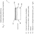
- the schematically shown component 1 has a silicon-based arrangement 100, shown in cross section, according to the concept of the invention, which is designed for generating a difference or sum frequency, in the present case a terahertz signal.
- the arrangement 100 embodied as a layer arrangement has a first layer of a material 104 with a first refractive index n 1 and a double layer of a silicon material consisting of an EO active layer 102 and an EO inactive layer 103, each of which has a second refractive index n 2 .
- Layer 102 has a chemical surface modification 101 in the form of silicon-halogen bonds, which causes the EO activity of layer 102.
- the refractive index n 1 of the material 104 is in any case lower than the refractive index n 2 of the silicon material 102, in the present case the silicon material consisting of 102 and 103.
- the optical excitation mode is restricted to the layer of silicon material 102 and 103 in the direction of propagation of the excitation mode.
- Modifications and improvements according to various embodiments of an EO device, particularly the waveguide are as follows 2 to 6 explained. These serve, in particular, to increase the intensity of the optical mode in the EO active silicon material 102 and on its surface 101 and to guide the excitation signal and the generated THz signal in a phase-adapted manner.
- EO component not only as a waveguide, but also, for example, as a radiation source, detector and / or electro-optical modulator for a signal in the millimeter wavelength range, terahertz frequency range and / or infrared range.
- the detection or radiation generation can in turn be carried out by an optical signal coupling, without the component 1 having to be designed as a laterally delimited waveguide.
- the ⁇ (2) effect (the named second-order EO activity) of a signal generation in the millimeter-wave range, terahertz frequency range and / or infrared range on the surface of the EO active silicon material 102 is, as it turns out, very considerably increased as a result of a chemically modified surface 101 with the help of a halogen enrichment.
- halogens fluorine, chlorine, bromine and iodine, bromine has proven to be particularly effective.
- the bromine enrichment is formed as a real chemical bond between atomic bromine and silicon on the surface and leads to an atomic charge shift (polarization) on the surface 101 which is advantageous for the ⁇ (2) effect.
- bromine In contrast to other halogens, bromine has particularly advantageous properties for the formation of the atomic dipole layer and the atomic charge shift as part of a bromine-silicon bond on the surface 101, such as high surface density, homogeneity and thermal stability.
- the surface 101 has been plasma activated for bromine enrichment in the present embodiment, namely in the context of a RIE dry plasma etching method known per se.
- pure HBr was used for the activation of dry plasma without additional gases.
- the surface 101 is conditioned practically instantaneously with bromine enrichment. Oxide is advantageously removed from the surface by ion bombardment, so that a bromine bond can take place largely unhindered. Excess unbound bromine escapes practically instantaneously under atmospheric conditions and a surface 101 enriched with bromine-silicon bonds remains.
- the surface 101 can also be conditioned in the course of a wet chemical etching process, for example by splitting the silicon surface in a bromine-containing solution or after cleaning, e.g. B. HF cleaning to remove oxides or by electrochemical etching in a Br-HF solution.
- a wet chemical etching process for example by splitting the silicon surface in a bromine-containing solution or after cleaning, e.g. B. HF cleaning to remove oxides or by electrochemical etching in a Br-HF solution.
- the basic structure of the in Fig. 1 described EO component 1 can advantageously also with a waveguide 2 to 6 which are described below in a second to sixth embodiment.
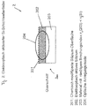
- Fig. 2 shows an EO component 2 in the form of a waveguide arrangement with a silicon-based arrangement 200 shown in cross section. This is formed from a material 203 with a first refractive index n 1 , an EO active silicon material 202 with a second refractive index n 2 and one as in FIG Fig. 1 described chemically modified surface 201 with a bromine enrichment.
- n 2 refractive index
- n 1 n 1
- an optical excitation mode 204 is strongly limited to the layer of the electro-optically active silicon material 202 and its surface 201 with the bromine enrichment.
- the layer thickness of the electro-optically active silicon material 202 in the present case is 200 nm, while the layer thickness of the material 203 with a low refractive index n 1 is 2 ⁇ m.
- the material with a low refractive index is formed from a silicon oxide.
- Other embodiments, which are not shown here, can also, for example, be a material based on cyclo-olefin copolymer (COC) or a benzocyclobutene (BCB), an SU8 or a PMMA or other transparent polymer.
- the material 203 with a low first refractive index n 1 is comparatively thick compared to the EO Active silicon material 202 is designed to ensure low-loss guidance of the optical excitation mode and a strong interaction of the excitation mode 204 guided in the EO active silicon material 202 to the dipoles of the silicon-bromine bonds on the surface 201.
- the material 203 of low refractive index has a larger band gap than silicon.
- the silicon-based arrangement 200 has a sufficient length of 5 mm in the present case for the formation of a waveguide.
- a similar extension of a waveguide arrangement in the range of 1-10 mm can prove to be sufficient.
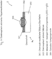
- FIG. 3 A further electro-optical component 3 with a silicon-based arrangement 300 is shown in cross-section, which essentially corresponds to the arrangement 200 in terms of the materials Fig. 2 corresponds.
- the EO active silicon material 302 is formed in a rib structure, so that the optical excitation mode 304 is also narrowly limited laterally to the EO active silicon material 302.
- this further increase in intensity is supported by the low refractive index of the material 303, its optical Transparency and the significantly thicker design of the material 303 compared to the EO active silicon material 302.
- the component 4 of the Fig. 4 again serves to form a waveguide with a silicon-based arrangement 400.
- the chemically modified surface 401 of the EO active silicon material 402 can have a laterally smaller dimension than the underlying material 403 with a low first refractive index n 1 . This also leads to a sufficient Intensity increase of the optical excitation mode 404.
- the in Fig. 4 The arrangement 400 shown is particularly suitable for forming a strip waveguide.
- Fig. 5 shows a fifth embodiment of an EO component 5 in the form of a waveguide, in which the arrangement 500 shown in cross section practically corresponds to the arrangement 300 of the component 3 of FIG Fig. 3 contains.
- the free height of the optical excitation mode 504 is also exposed to an additional intensity increase in that a material 503 with a low refractive index n 1 is in turn applied above the EO-active silicon material 502.
- a metal layer 505 in the form of a single strip line is applied over the material 503 and enables the generated THz signal to be routed.
- a phase-adjusted guidance of the generated THz signal is of great importance in order to achieve maximum conversion efficiency.
- the wavelength of the generated signal can be several orders of magnitude above the wavelength of the pump signal.
- the EO-active silicon material 502 is here surrounded on both sides by a material with a lower refractive index, which enables the undisturbed, low-loss guidance of the excitation mode 504 by a sufficient distance from the metal layer 505.
- the EO component 6 shown has a silicon-based arrangement 600, which in its core essentially corresponds to the arrangement 300 for the component 3, which is why here only a general reference to the corresponding reference numerals 603 (303), 602 (302), 601 (301) and 604 (304 ) Is referenced.
- the arrangement 600 shown in cross section is designed such that the material 603 with a low refractive index n 1 is arranged on a silicon substrate 605 and is provided with a passivation layer 606 together with the silicon substrate 605.
- a generated signal with a longer wavelength than the pump wavelength can be guided by the shape of the cross-sectional profile of material 605, which here forms a dielectric ribbed waveguide.
- arrangement 600 is designed as a purely dielectric hybrid waveguide.
- the following processes can be used to produce the electro-optically activated surface 601 (301) with silicon halogen bonds:
- a gas plasma e.g. B. in a pure HBr plasma with a gas flow of 40 sccm, a process duration of 3-4 sec, a chamber pressure of about 6mTorr and 100 W RF and 250 W ICP power.
- wet chemical activation the silicon surface is first freed of oxides, e.g. B. in hydrofluoric acid. Then the silicon surface is placed in a weak Br-methanol solution for approx. 60 min, bromine atoms attaching to the silicon interface atoms.
- Fig. 7 uses an SHG signal (Second Harmonic Generation) to demonstrate the arrangement of SiBr bonds on an HBr-activated Si surface (upper curve). Without HBr activation, only the background level can be measured.
- SHG signal Signal Harmonic Generation
- Fig. 8 illustrates the gigantic amplitude of a THz signal from an HBr-activated Si surface compared to a standard THz emitter InGaAs bulk material.
- the pump power is about 50-100 ⁇ W in both cases.
- the Hbr-activated Si surface - in the present case with a waveguide - is surprisingly non-linearly optically active.
Landscapes
- Physics & Mathematics (AREA)
- Nonlinear Science (AREA)
- Optics & Photonics (AREA)
- Chemical & Material Sciences (AREA)
- Engineering & Computer Science (AREA)
- Nanotechnology (AREA)
- General Physics & Mathematics (AREA)
- Life Sciences & Earth Sciences (AREA)
- Biophysics (AREA)
- Crystallography & Structural Chemistry (AREA)
- Optical Modulation, Optical Deflection, Nonlinear Optics, Optical Demodulation, Optical Logic Elements (AREA)
- Optical Integrated Circuits (AREA)
Claims (19)
- Composant (1, 2, 3, 4, 5, 6) électro-optique ayant un agencement (100, 200, 300, 400, 500, 600) à base de silicium et/ou de germanium, dans lequel
l'agencement (100, 200, 300, 400, 500, 600) à base de silicium et/ou de germanium a un volume de matériau et un matériau (104, 203, 303, 403, 503, 603) voisin,
le volume de matériau est en silicium et/ou en germanium et, en conséquence, a une surface (101, 201, 301, 401, 501, 601) en silicium et/ou en germanium,
dans lequel
la surface (101, 201, 301, 401, 501, 601) est modifiée chimiquement par un enrichissement en halogène, dans lequel
l'agencement (100, 200, 300, 400, 500, 600) a base de silicium et/ou de germanium a une couche du matériau (104, 203, 303, 403, 503, 603) voisin ayant un premier indice n1 de réfraction et a une couche double dans le volume de matériau, le volume de matériau étant constitué d'une couche (102, 202, 302, 402, 502, 602) active électro-optiquement et d'une couche (103) inactive électro-optiquement qui ont chacune un deuxième indice n2 de réfraction, la couche (102, 2023, 302, 402, 502, 602) active électro-optiquement, qui possède la modification (101, 201, 301, 401, 501, 601) chimique de surface, possédant des composés sous forme de silicium-halogène et/ou germanium-halogène qui provoquent l'activité électro-optique de la couche (102, 202, 302, 402, 502, 602) active électro-optiquement,
et dans lequel
le volume de matériau est déposé sur le matériau (104, 203, 303, 403, 503, 603) voisin pour former un agencement de guide d'onde et
le deuxième indice n2 de réfraction est plus grand que le premier indice n1 de réfraction. - Composant (1, 2, 3, 4, 5, 6) suivant la revendication 1, caractérisé en ce que l'enrichissement en halogène est choisi sous la forme d'un enrichissement en un ou en plusieurs enrichissements choisis dans le groupe constitué d'un enrichissement en brome, d'un enrichissement en fluor, d'un enrichissement en chlore.
- Composant (1, 2, 3, 4, 5, 6) suivant la revendication 1 ou 2, caractérisé en ce que l'enrichissement en halogène modifie la surface par une liaison covalente de l'halogène sur un atome de silicium et/ou de germanium de la surface et notamment l'halogène enrichit la surface sous forme atomique.
- Composant (1, 2, 3, 4, 5, 6) suivant l'une des revendications 1 à 3, caractérisé en ce que la couche (103) inactive électro-optiquement est disposée entre la couche (102, 202, 302, 402, 502, 602) active électro-optiquement et le matériau (104, 203, 303, 403, 503, 603) voisin.
- Composant (1, 2, 3, 4, 5, 6) suivant la revendication 1, caractérisé en ce que le premier indice n1 de réfraction est dans la plage de n1 = 1 à n1 = 2,5 en étant sensiblement plus petit que le deuxième indice n2 de réfraction dans la plage de n2 = 3, 4 à n2 = 3,6.
- Composant (1, 2, 3, 4, 5, 6) suivant l'une des revendications 1 à 5, caractérisé en ce que, dans le stratifié de l'agencement de couche (100, 200, 300, 400, 500, 600) à base de silicium et/ou de germanium, la couche (102, 202, 302, 402, 502, 602) active électro-optiquement a une épaisseur dans la plage de 50 à 300 nm et notamment dans la plage de 100 à 200 nm.
- Composant (1, 2, 3, 4, 5, 6) suivant l'une des revendications 1 à 6, caractérisé en ce que la couche du matériau (104, 203, 303, 403, 503, 603) voisin, ayant le premier indice n1 de réfraction plus petit, a une épaisseur qui est sensiblement plus grande que l'épaisseur de la couche (102, 202, 302, 402, 502, 602) active électro-optiquement.
- Composant (1, 2, 3, 4, 5, 6) suivant l'une des revendications 1 à 7, caractérisé en ce que la couche du matériau (104, 203, 303, 403, 503, 603) voisin, ayant le premier indice n1 de réfraction, a une épaisseur dans la plage de 0,5 à 4 µm et notamment dans la plage de 1 à 3 µm.
- Composant (1, 2, 3, 4, 5, 6) suivant l'une des revendications 1 à 8, caractérisé en ce que le matériau (104, 203, 303, 403, 503, 603) voisin, ayant le premier indice n1 de réfraction plus petit, est un matériau transparent optiquement au-dessus des longueurs d'onde de 1,1 µm.
- Composant (1, 2, 3, 4, 5, 6) suivant la revendication 9, caractérisé en ce que le matériau transparent optiquement est choisi dans le groupe constitué de : SiO2, un polymère transparent, un polymère cyclo-oléfinique (COC), un benzo-cyclo-butène, un SUB et un PMMA.
- Composant (1, 2, 3, 4, 5, 6) suivant l'une des revendications 1 à 10, caractérisé en ce que la couche (102, 202, 302, 402, 502, 602) active électro-optiquement forme une couche plane ou a une structure nervurée et, s'il y a une structure nervurée, il est formé notamment un guide d'onde sous la forme d'un guide d'onde nervuré.
- Composant (1, 2, 3, 4, 5, 6) suivant l'une des revendications 1 à 11, caractérisé en ce que l'agencement (100, 200, 300, 400, 500, 600) à base de silicium et/ou de germanium fait partie d'une structure MESA, un guide d'onde sous la forme d'un guide d'onde à ruban étant notamment formé et, de préférence, la couche (102) active électro-optiquement a une dimension latérale plus petite que le matériau (104, 203, 303, 403, 503, 603) voisin.
- Composant (1, 2, 3, 4, 5, 6) suivant l'une des revendications 1 à 12, caractérisé en ce que, sur l'agencement (100, 200, 300, 400, 500, 600) à base de silicium et/ou de germanium, est formé un recouvrement métallique et/ou diélectrique et il est formé notamment un guide d'onde sous la forme d'un guide d'onde hybride ayant un recouvrement métallique et/ou diélectrique et/ou le composant (1, 2, 3, 4, 5, 6) est caractérisé par une couche (606) de passivation.
- Composant (1, 2, 3, 4, 5, 6) suivant l'une des revendications 1 à 13, caractérisé en ce que l'agencement (100, 200, 300, 400, 500) à base de silicium et/ou de germanium est formé d'un substrat en silicium et/ou en germanium.
- Composant (1, 2, 3, 4, 5, 6) suivant l'une des revendications 1 à 14, caractérisé en ce que la couche (102, 202, 302, 402, 502, 602) active électro-optiquement est, par rapport au matériau (104, 203, 303, 403, 503, 603) voisin ayant l'indice n1 de réfraction plus petit, bloquée mécaniquement et/ou polarisée électriquement.
- Agencement de guide d'onde ou détecteur et/ou modulateur ou source de rayonnement ou système de mesure et/ou de détection comprenant un composant (1, 2, 3, 4, 5, 6) suivant l'une des revendications 1 à 15, dans lequel notamment un agencement de guide d'onde est conçu pour la production optique de signaux dans le domaine des longueurs d'onde du millimètre, le domaine de séquence du térahertz et/ou le domaine infrarouge et/ou dans lequel l'étendue longitudinale de l'agencement de guide d'onde est dans la plage de 1 à 10 mm.
- Procédé de production d'un composant (1, 2, 3, 4, 5, 6) électro-optique suivant l'une des revendications précédentes, comprenant les stades :- on se procure un matériau (104, 203, 303, 403, 503, 603) ayant un premier indice n1 de réfraction ;- on dépose un silicium et/ou un germanium à activer électro-optiquement d'un deuxième indice n2 de réfraction comme matériau de volume et ayant une surface (101, 201, 301, 401, 501, 601) ;- on modifie chimiquement la surface (101, 201, 301, 401, 501, 601) par un enrichissement en halogène de manière à activer électro-optiquement le silicium et/ou le germanium ;- on réalise l'agencement (100, 200, 300, 400, 500, 600) de silicium et/ou de germanium sous la forme d'un stratifié, une couche du matériau (104, 203, 303, 403, 503, 603) ayant le premier indice n1 de réfraction et une couche double dans le volume de matériau en une couche (102, 302, 402, 502, 602) active électro-optiquement et en une couche (103) inactive électro-optiquement, qui ont chacune un deuxième indice n2 de réfraction, étant réalisées, la couche (102, 202, 302, 402, 502, 602) active électro-optiquement possédant la modification (101, 201, 301, 401, 501, 601) de surface sous la forme de composés de silicium et/ou germanium-halogène, qui provoque l'activité électro-optique de la couche (102, 202, 302, 402, 502, 602) active électro-optiquement,
et dans lequel
on dépose le volume de matériau sur le matériau (104, 203, 303, 403, 503, 603) ayant le premier indice n1 de réfraction pour former un agencement de guide d'onde, dans lequel
le deuxième indice n2 de réfraction est plus grand que le premier indice n1 de réfraction. - Procédé de production suivant la revendication 17, caractérisé en ce que l'on met le matériau (104, 203, 303, 403, 503, 603), ayant le premier indice n1 de réfraction plus petit, entre la couche (102, 202, 302, 402, 502, 602) active électro-optiquement et un substrat (605) en silicium et/ou en germanium, dans lequel le premier indice n1 de réfraction est sensiblement plus petit que le deuxième indice n2 de réfraction de la couche (102, 202, 302, 402, 502, 602) active électro-optiquement.
- Procédé de production suivant la revendication 17 ou 18, caractérisé en ce que l'on traite la surface (101, 201, 301, 401, 501, 601) chimiquement en voie humide et/ou on l'active par plasma dans un procédé au plasma, notamment dans un procédé au plasma sec ou dans un procédé RIE.
Applications Claiming Priority (2)
| Application Number | Priority Date | Filing Date | Title |
|---|---|---|---|
| DE102009045037A DE102009045037A1 (de) | 2009-09-25 | 2009-09-25 | Elektrooptisches Bauelement, Verwendung und Herstellung des Bauelements |
| PCT/EP2010/064143 WO2011036250A1 (fr) | 2009-09-25 | 2010-09-24 | Composant électro-optique, utilisation et production de ce composant |
Publications (2)
| Publication Number | Publication Date |
|---|---|
| EP2480932A1 EP2480932A1 (fr) | 2012-08-01 |
| EP2480932B1 true EP2480932B1 (fr) | 2020-07-08 |
Family
ID=43332993
Family Applications (1)
| Application Number | Title | Priority Date | Filing Date |
|---|---|---|---|
| EP10757764.5A Active EP2480932B1 (fr) | 2009-09-25 | 2010-09-24 | Composant électro-optique et production du composant |
Country Status (3)
| Country | Link |
|---|---|
| EP (1) | EP2480932B1 (fr) |
| DE (1) | DE102009045037A1 (fr) |
| WO (1) | WO2011036250A1 (fr) |
Families Citing this family (1)
| Publication number | Priority date | Publication date | Assignee | Title |
|---|---|---|---|---|
| WO2011129690A2 (fr) | 2010-04-13 | 2011-10-20 | Nederlandse Organisatie Voor Toegepast-Natuurwetenschappelijk Onderzoek Tno | Générateur de rayonnement à fréquence terahertz |
Family Cites Families (5)
| Publication number | Priority date | Publication date | Assignee | Title |
|---|---|---|---|---|
| US5246734A (en) * | 1986-05-05 | 1993-09-21 | Dow Corning Corporation | Amorphous silicon hermetic coatings for optical wave guides |
| FR2817630B1 (fr) | 2000-12-01 | 2003-04-11 | Thomson Csf | Dispositif d'emission d'onde lumineuse dans la gamme du teraherz |
| US6549685B2 (en) * | 2001-01-31 | 2003-04-15 | Northwestern University | High-response electro-optic modulator based on an intrinsically acentric, layer-by-layer self-assembled molecular superlattice |
| US20020192969A1 (en) * | 2001-04-26 | 2002-12-19 | Becky Losee | Method for etching silicon trenches |
| EP2033028A4 (fr) * | 2006-05-31 | 2011-05-04 | Georgia Tech Res Inst | Sondes de detection integrees, procedes de fabrication et procedes d'utilisation de celles-ci |
-
2009
- 2009-09-25 DE DE102009045037A patent/DE102009045037A1/de not_active Ceased
-
2010
- 2010-09-24 EP EP10757764.5A patent/EP2480932B1/fr active Active
- 2010-09-24 WO PCT/EP2010/064143 patent/WO2011036250A1/fr not_active Ceased
Non-Patent Citations (1)
| Title |
|---|
| None * |
Also Published As
| Publication number | Publication date |
|---|---|
| DE102009045037A1 (de) | 2011-03-31 |
| EP2480932A1 (fr) | 2012-08-01 |
| WO2011036250A1 (fr) | 2011-03-31 |
Similar Documents
| Publication | Publication Date | Title |
|---|---|---|
| DE69417611T2 (de) | Verfahren zum stabilen Betrieb eines aktiven modengekoppelten optischen Faser-Lasers | |
| DE69117728T2 (de) | Optischer verstärker | |
| DE2812955A1 (de) | Nichtlineare optische duennschichtvorrichtung und verfahren zu ihrer herstellung | |
| DE68924188T2 (de) | Optischer Wellenlängenkonverter. | |
| DE102016102839B4 (de) | Faserübertragung von kurzen Laserimpulsen | |
| DE69409564T2 (de) | Halbleiterlaser und Modulationsverfahren | |
| DE112016006006T5 (de) | Optische Vorrichtung und Verfahren zur Herstellung der optischen Vorrichtung | |
| DE102008047226A1 (de) | Vorrichtung zum Verstärken von Lichtimpulsen | |
| DE68910883T2 (de) | Vorrichtung zur Erzeugung optischer Oberwellen. | |
| DE102013210438B4 (de) | Quantenkaskadenlaser | |
| DE69903844T2 (de) | Herstellung von lichtwellenleitern | |
| DE112017006644T5 (de) | Optische Vorrichtung, Verfahren zum Herstellen einer optischen Vorrichtung undWellenlängenumwandlungsverfahren | |
| EP3545347A2 (fr) | Composant optoélectronique et procédé de fabrication d'un composant optoélectronique | |
| DE102010048576B4 (de) | Laservorrichtung zur Erzeugung eines CEO-freien Frequenzkamms | |
| DE69214029T2 (de) | Polarisationsfilter | |
| DE102009045037A1 (de) | Elektrooptisches Bauelement, Verwendung und Herstellung des Bauelements | |
| DE202021105216U1 (de) | Lasergerät auf Basis von Aluminiumnitrid-Nanodrähten | |
| DE69002974T2 (de) | Optische Faser zur Frequenzumwandlung. | |
| DE102020118780B4 (de) | Anordnung und verfahren zur effizienten nichtlinearen lichtkonversion | |
| DE102020125544A1 (de) | Erzeugung von ultrakurzen Laserpulsen | |
| DE60000851T2 (de) | Halbleiterlaser mit parametrischer Lichterzeugung | |
| EP2656141B1 (fr) | Conversion de fréquence efficace | |
| EP3776076B1 (fr) | Fabrication de guides d'onde avec des matériaux de la famille des ktp | |
| DE102018128538A1 (de) | Fahrerassistenzsystem mit einem Sender mit einer frequenzgesteuerten Abstrahlrichtung und einem Konverter zur Frequenzangleichung | |
| DE10322110B4 (de) | Anordnung zur Erzeugung von optischen Mehrwellensignalen und Mehrsignal-Quelle |
Legal Events
| Date | Code | Title | Description |
|---|---|---|---|
| PUAI | Public reference made under article 153(3) epc to a published international application that has entered the european phase |
Free format text: ORIGINAL CODE: 0009012 |
|
| 17P | Request for examination filed |
Effective date: 20120425 |
|
| AK | Designated contracting states |
Kind code of ref document: A1 Designated state(s): AL AT BE BG CH CY CZ DE DK EE ES FI FR GB GR HR HU IE IS IT LI LT LU LV MC MK MT NL NO PL PT RO SE SI SK SM TR |
|
| DAX | Request for extension of the european patent (deleted) | ||
| RAP1 | Party data changed (applicant data changed or rights of an application transferred) |
Owner name: GESELLSCHAFT FUER ANGEWANDTE MIKRO- UND OPTOELEKTR |
|
| STAA | Information on the status of an ep patent application or granted ep patent |
Free format text: STATUS: EXAMINATION IS IN PROGRESS |
|
| 17Q | First examination report despatched |
Effective date: 20170302 |
|
| GRAP | Despatch of communication of intention to grant a patent |
Free format text: ORIGINAL CODE: EPIDOSNIGR1 |
|
| STAA | Information on the status of an ep patent application or granted ep patent |
Free format text: STATUS: GRANT OF PATENT IS INTENDED |
|
| RIC1 | Information provided on ipc code assigned before grant |
Ipc: G02F 1/355 20060101ALI20191217BHEP Ipc: G02F 1/35 20060101AFI20191217BHEP Ipc: H01L 21/306 20060101ALI20191217BHEP Ipc: B82Y 20/00 20110101ALN20191217BHEP |
|
| INTG | Intention to grant announced |
Effective date: 20200121 |
|
| GRAS | Grant fee paid |
Free format text: ORIGINAL CODE: EPIDOSNIGR3 |
|
| GRAA | (expected) grant |
Free format text: ORIGINAL CODE: 0009210 |
|
| STAA | Information on the status of an ep patent application or granted ep patent |
Free format text: STATUS: THE PATENT HAS BEEN GRANTED |
|
| AK | Designated contracting states |
Kind code of ref document: B1 Designated state(s): AL AT BE BG CH CY CZ DE DK EE ES FI FR GB GR HR HU IE IS IT LI LT LU LV MC MK MT NL NO PL PT RO SE SI SK SM TR |
|
| REG | Reference to a national code |
Ref country code: GB Ref legal event code: FG4D Free format text: NOT ENGLISH |
|
| REG | Reference to a national code |
Ref country code: CH Ref legal event code: EP Ref country code: AT Ref legal event code: REF Ref document number: 1289089 Country of ref document: AT Kind code of ref document: T Effective date: 20200715 |
|
| REG | Reference to a national code |
Ref country code: DE Ref legal event code: R096 Ref document number: 502010016687 Country of ref document: DE |
|
| REG | Reference to a national code |
Ref country code: IE Ref legal event code: FG4D Free format text: LANGUAGE OF EP DOCUMENT: GERMAN |
|
| REG | Reference to a national code |
Ref country code: LT Ref legal event code: MG4D |
|
| REG | Reference to a national code |
Ref country code: NL Ref legal event code: MP Effective date: 20200708 |
|
| PG25 | Lapsed in a contracting state [announced via postgrant information from national office to epo] |
Ref country code: FI Free format text: LAPSE BECAUSE OF FAILURE TO SUBMIT A TRANSLATION OF THE DESCRIPTION OR TO PAY THE FEE WITHIN THE PRESCRIBED TIME-LIMIT Effective date: 20200708 Ref country code: BG Free format text: LAPSE BECAUSE OF FAILURE TO SUBMIT A TRANSLATION OF THE DESCRIPTION OR TO PAY THE FEE WITHIN THE PRESCRIBED TIME-LIMIT Effective date: 20201008 Ref country code: SE Free format text: LAPSE BECAUSE OF FAILURE TO SUBMIT A TRANSLATION OF THE DESCRIPTION OR TO PAY THE FEE WITHIN THE PRESCRIBED TIME-LIMIT Effective date: 20200708 Ref country code: NO Free format text: LAPSE BECAUSE OF FAILURE TO SUBMIT A TRANSLATION OF THE DESCRIPTION OR TO PAY THE FEE WITHIN THE PRESCRIBED TIME-LIMIT Effective date: 20201008 Ref country code: PT Free format text: LAPSE BECAUSE OF FAILURE TO SUBMIT A TRANSLATION OF THE DESCRIPTION OR TO PAY THE FEE WITHIN THE PRESCRIBED TIME-LIMIT Effective date: 20201109 Ref country code: GR Free format text: LAPSE BECAUSE OF FAILURE TO SUBMIT A TRANSLATION OF THE DESCRIPTION OR TO PAY THE FEE WITHIN THE PRESCRIBED TIME-LIMIT Effective date: 20201009 Ref country code: ES Free format text: LAPSE BECAUSE OF FAILURE TO SUBMIT A TRANSLATION OF THE DESCRIPTION OR TO PAY THE FEE WITHIN THE PRESCRIBED TIME-LIMIT Effective date: 20200708 Ref country code: LT Free format text: LAPSE BECAUSE OF FAILURE TO SUBMIT A TRANSLATION OF THE DESCRIPTION OR TO PAY THE FEE WITHIN THE PRESCRIBED TIME-LIMIT Effective date: 20200708 Ref country code: HR Free format text: LAPSE BECAUSE OF FAILURE TO SUBMIT A TRANSLATION OF THE DESCRIPTION OR TO PAY THE FEE WITHIN THE PRESCRIBED TIME-LIMIT Effective date: 20200708 |
|
| PG25 | Lapsed in a contracting state [announced via postgrant information from national office to epo] |
Ref country code: PL Free format text: LAPSE BECAUSE OF FAILURE TO SUBMIT A TRANSLATION OF THE DESCRIPTION OR TO PAY THE FEE WITHIN THE PRESCRIBED TIME-LIMIT Effective date: 20200708 Ref country code: LV Free format text: LAPSE BECAUSE OF FAILURE TO SUBMIT A TRANSLATION OF THE DESCRIPTION OR TO PAY THE FEE WITHIN THE PRESCRIBED TIME-LIMIT Effective date: 20200708 Ref country code: IS Free format text: LAPSE BECAUSE OF FAILURE TO SUBMIT A TRANSLATION OF THE DESCRIPTION OR TO PAY THE FEE WITHIN THE PRESCRIBED TIME-LIMIT Effective date: 20201108 |
|
| PG25 | Lapsed in a contracting state [announced via postgrant information from national office to epo] |
Ref country code: NL Free format text: LAPSE BECAUSE OF FAILURE TO SUBMIT A TRANSLATION OF THE DESCRIPTION OR TO PAY THE FEE WITHIN THE PRESCRIBED TIME-LIMIT Effective date: 20200708 |
|
| REG | Reference to a national code |
Ref country code: DE Ref legal event code: R097 Ref document number: 502010016687 Country of ref document: DE |
|
| PG25 | Lapsed in a contracting state [announced via postgrant information from national office to epo] |
Ref country code: MC Free format text: LAPSE BECAUSE OF FAILURE TO SUBMIT A TRANSLATION OF THE DESCRIPTION OR TO PAY THE FEE WITHIN THE PRESCRIBED TIME-LIMIT Effective date: 20200708 Ref country code: SM Free format text: LAPSE BECAUSE OF FAILURE TO SUBMIT A TRANSLATION OF THE DESCRIPTION OR TO PAY THE FEE WITHIN THE PRESCRIBED TIME-LIMIT Effective date: 20200708 Ref country code: RO Free format text: LAPSE BECAUSE OF FAILURE TO SUBMIT A TRANSLATION OF THE DESCRIPTION OR TO PAY THE FEE WITHIN THE PRESCRIBED TIME-LIMIT Effective date: 20200708 Ref country code: IT Free format text: LAPSE BECAUSE OF FAILURE TO SUBMIT A TRANSLATION OF THE DESCRIPTION OR TO PAY THE FEE WITHIN THE PRESCRIBED TIME-LIMIT Effective date: 20200708 Ref country code: DK Free format text: LAPSE BECAUSE OF FAILURE TO SUBMIT A TRANSLATION OF THE DESCRIPTION OR TO PAY THE FEE WITHIN THE PRESCRIBED TIME-LIMIT Effective date: 20200708 Ref country code: EE Free format text: LAPSE BECAUSE OF FAILURE TO SUBMIT A TRANSLATION OF THE DESCRIPTION OR TO PAY THE FEE WITHIN THE PRESCRIBED TIME-LIMIT Effective date: 20200708 Ref country code: CZ Free format text: LAPSE BECAUSE OF FAILURE TO SUBMIT A TRANSLATION OF THE DESCRIPTION OR TO PAY THE FEE WITHIN THE PRESCRIBED TIME-LIMIT Effective date: 20200708 |
|
| REG | Reference to a national code |
Ref country code: CH Ref legal event code: PL |
|
| PLBE | No opposition filed within time limit |
Free format text: ORIGINAL CODE: 0009261 |
|
| STAA | Information on the status of an ep patent application or granted ep patent |
Free format text: STATUS: NO OPPOSITION FILED WITHIN TIME LIMIT |
|
| PG25 | Lapsed in a contracting state [announced via postgrant information from national office to epo] |
Ref country code: AL Free format text: LAPSE BECAUSE OF FAILURE TO SUBMIT A TRANSLATION OF THE DESCRIPTION OR TO PAY THE FEE WITHIN THE PRESCRIBED TIME-LIMIT Effective date: 20200708 |
|
| 26N | No opposition filed |
Effective date: 20210409 |
|
| REG | Reference to a national code |
Ref country code: BE Ref legal event code: MM Effective date: 20200930 |
|
| PG25 | Lapsed in a contracting state [announced via postgrant information from national office to epo] |
Ref country code: LU Free format text: LAPSE BECAUSE OF NON-PAYMENT OF DUE FEES Effective date: 20200924 Ref country code: SK Free format text: LAPSE BECAUSE OF FAILURE TO SUBMIT A TRANSLATION OF THE DESCRIPTION OR TO PAY THE FEE WITHIN THE PRESCRIBED TIME-LIMIT Effective date: 20200708 |
|
| PG25 | Lapsed in a contracting state [announced via postgrant information from national office to epo] |
Ref country code: BE Free format text: LAPSE BECAUSE OF NON-PAYMENT OF DUE FEES Effective date: 20200930 Ref country code: CH Free format text: LAPSE BECAUSE OF NON-PAYMENT OF DUE FEES Effective date: 20200930 Ref country code: SI Free format text: LAPSE BECAUSE OF FAILURE TO SUBMIT A TRANSLATION OF THE DESCRIPTION OR TO PAY THE FEE WITHIN THE PRESCRIBED TIME-LIMIT Effective date: 20200708 Ref country code: LI Free format text: LAPSE BECAUSE OF NON-PAYMENT OF DUE FEES Effective date: 20200930 Ref country code: IE Free format text: LAPSE BECAUSE OF NON-PAYMENT OF DUE FEES Effective date: 20200924 |
|
| REG | Reference to a national code |
Ref country code: AT Ref legal event code: MM01 Ref document number: 1289089 Country of ref document: AT Kind code of ref document: T Effective date: 20200924 |
|
| PG25 | Lapsed in a contracting state [announced via postgrant information from national office to epo] |
Ref country code: AT Free format text: LAPSE BECAUSE OF NON-PAYMENT OF DUE FEES Effective date: 20200924 |
|
| PG25 | Lapsed in a contracting state [announced via postgrant information from national office to epo] |
Ref country code: TR Free format text: LAPSE BECAUSE OF FAILURE TO SUBMIT A TRANSLATION OF THE DESCRIPTION OR TO PAY THE FEE WITHIN THE PRESCRIBED TIME-LIMIT Effective date: 20200708 Ref country code: MT Free format text: LAPSE BECAUSE OF FAILURE TO SUBMIT A TRANSLATION OF THE DESCRIPTION OR TO PAY THE FEE WITHIN THE PRESCRIBED TIME-LIMIT Effective date: 20200708 Ref country code: CY Free format text: LAPSE BECAUSE OF FAILURE TO SUBMIT A TRANSLATION OF THE DESCRIPTION OR TO PAY THE FEE WITHIN THE PRESCRIBED TIME-LIMIT Effective date: 20200708 |
|
| PG25 | Lapsed in a contracting state [announced via postgrant information from national office to epo] |
Ref country code: MK Free format text: LAPSE BECAUSE OF FAILURE TO SUBMIT A TRANSLATION OF THE DESCRIPTION OR TO PAY THE FEE WITHIN THE PRESCRIBED TIME-LIMIT Effective date: 20200708 |
|
| PGFP | Annual fee paid to national office [announced via postgrant information from national office to epo] |
Ref country code: GB Payment date: 20250923 Year of fee payment: 16 |
|
| PGFP | Annual fee paid to national office [announced via postgrant information from national office to epo] |
Ref country code: FR Payment date: 20250926 Year of fee payment: 16 |
|
| PGFP | Annual fee paid to national office [announced via postgrant information from national office to epo] |
Ref country code: DE Payment date: 20251007 Year of fee payment: 16 |
|
| REG | Reference to a national code |
Ref country code: DE Ref legal event code: R082 Ref document number: 502010016687 Country of ref document: DE Representative=s name: EISENFUEHR SPEISER PATENTANWAELTE RECHTSANWAEL, DE |