EP2479142A1 - Polycrystalline silicon mass and process for producing polycrystalline silicon mass - Google Patents
Polycrystalline silicon mass and process for producing polycrystalline silicon mass Download PDFInfo
- Publication number
- EP2479142A1 EP2479142A1 EP10816827A EP10816827A EP2479142A1 EP 2479142 A1 EP2479142 A1 EP 2479142A1 EP 10816827 A EP10816827 A EP 10816827A EP 10816827 A EP10816827 A EP 10816827A EP 2479142 A1 EP2479142 A1 EP 2479142A1
- Authority
- EP
- European Patent Office
- Prior art keywords
- polycrystalline silicon
- mass
- concentrations
- silicon mass
- rod
- Prior art date
- Legal status (The legal status is an assumption and is not a legal conclusion. Google has not performed a legal analysis and makes no representation as to the accuracy of the status listed.)
- Granted
Links
- 229910021420 polycrystalline silicon Inorganic materials 0.000 title claims abstract description 210
- 238000000034 method Methods 0.000 title claims abstract description 59
- XEEYBQQBJWHFJM-UHFFFAOYSA-N Iron Chemical compound [Fe] XEEYBQQBJWHFJM-UHFFFAOYSA-N 0.000 claims abstract description 77
- PXHVJJICTQNCMI-UHFFFAOYSA-N Nickel Chemical compound [Ni] PXHVJJICTQNCMI-UHFFFAOYSA-N 0.000 claims abstract description 76
- 239000012535 impurity Substances 0.000 claims abstract description 48
- 239000011651 chromium Substances 0.000 claims abstract description 41
- 239000010949 copper Substances 0.000 claims abstract description 41
- 229910052804 chromium Inorganic materials 0.000 claims abstract description 40
- 229910052802 copper Inorganic materials 0.000 claims abstract description 40
- VYZAMTAEIAYCRO-UHFFFAOYSA-N Chromium Chemical compound [Cr] VYZAMTAEIAYCRO-UHFFFAOYSA-N 0.000 claims abstract description 39
- RYGMFSIKBFXOCR-UHFFFAOYSA-N Copper Chemical compound [Cu] RYGMFSIKBFXOCR-UHFFFAOYSA-N 0.000 claims abstract description 39
- 229910021421 monocrystalline silicon Inorganic materials 0.000 claims abstract description 39
- 229910052759 nickel Inorganic materials 0.000 claims abstract description 38
- 229910052742 iron Inorganic materials 0.000 claims abstract description 37
- 229910017052 cobalt Inorganic materials 0.000 claims abstract description 31
- 239000010941 cobalt Substances 0.000 claims abstract description 31
- GUTLYIVDDKVIGB-UHFFFAOYSA-N cobalt atom Chemical compound [Co] GUTLYIVDDKVIGB-UHFFFAOYSA-N 0.000 claims abstract description 31
- XUIMIQQOPSSXEZ-UHFFFAOYSA-N Silicon Chemical compound [Si] XUIMIQQOPSSXEZ-UHFFFAOYSA-N 0.000 claims description 43
- 238000005406 washing Methods 0.000 claims description 32
- VYPSYNLAJGMNEJ-UHFFFAOYSA-N Silicium dioxide Chemical compound O=[Si]=O VYPSYNLAJGMNEJ-UHFFFAOYSA-N 0.000 claims description 18
- 229910052710 silicon Inorganic materials 0.000 claims description 18
- 239000010703 silicon Substances 0.000 claims description 18
- 229910052814 silicon oxide Inorganic materials 0.000 claims description 13
- 238000000605 extraction Methods 0.000 claims description 12
- 238000007740 vapor deposition Methods 0.000 claims description 11
- XLYOFNOQVPJJNP-UHFFFAOYSA-N water Substances O XLYOFNOQVPJJNP-UHFFFAOYSA-N 0.000 claims description 11
- CBENFWSGALASAD-UHFFFAOYSA-N Ozone Chemical compound [O-][O+]=O CBENFWSGALASAD-UHFFFAOYSA-N 0.000 claims description 7
- 238000001095 inductively coupled plasma mass spectrometry Methods 0.000 claims description 6
- 230000003647 oxidation Effects 0.000 claims description 6
- 238000007254 oxidation reaction Methods 0.000 claims description 6
- 239000004698 Polyethylene Substances 0.000 claims description 3
- 238000000151 deposition Methods 0.000 claims description 3
- -1 polyethylene Polymers 0.000 claims description 3
- 229920000573 polyethylene Polymers 0.000 claims description 3
- 229910001385 heavy metal Inorganic materials 0.000 abstract description 31
- 229910052751 metal Inorganic materials 0.000 description 39
- 239000002184 metal Substances 0.000 description 39
- KRHYYFGTRYWZRS-UHFFFAOYSA-N Fluorane Chemical compound F KRHYYFGTRYWZRS-UHFFFAOYSA-N 0.000 description 14
- 238000011109 contamination Methods 0.000 description 13
- 239000002994 raw material Substances 0.000 description 13
- 150000002739 metals Chemical class 0.000 description 12
- 239000000243 solution Substances 0.000 description 11
- 239000013078 crystal Substances 0.000 description 10
- 238000005530 etching Methods 0.000 description 10
- 229910001220 stainless steel Inorganic materials 0.000 description 10
- 239000010935 stainless steel Substances 0.000 description 10
- 239000000463 material Substances 0.000 description 7
- 239000000969 carrier Substances 0.000 description 6
- 239000007788 liquid Substances 0.000 description 6
- 239000000126 substance Substances 0.000 description 6
- 239000001257 hydrogen Substances 0.000 description 5
- 229910052739 hydrogen Inorganic materials 0.000 description 5
- 238000005204 segregation Methods 0.000 description 5
- UFHFLCQGNIYNRP-UHFFFAOYSA-N Hydrogen Chemical compound [H][H] UFHFLCQGNIYNRP-UHFFFAOYSA-N 0.000 description 4
- MHAJPDPJQMAIIY-UHFFFAOYSA-N Hydrogen peroxide Chemical compound OO MHAJPDPJQMAIIY-UHFFFAOYSA-N 0.000 description 4
- 239000007864 aqueous solution Substances 0.000 description 4
- 239000007789 gas Substances 0.000 description 4
- 229910000040 hydrogen fluoride Inorganic materials 0.000 description 4
- 238000004519 manufacturing process Methods 0.000 description 4
- GRYLNZFGIOXLOG-UHFFFAOYSA-N Nitric acid Chemical compound O[N+]([O-])=O GRYLNZFGIOXLOG-UHFFFAOYSA-N 0.000 description 3
- 238000009434 installation Methods 0.000 description 3
- 239000011259 mixed solution Substances 0.000 description 3
- 229910017604 nitric acid Inorganic materials 0.000 description 3
- IJGRMHOSHXDMSA-UHFFFAOYSA-N nitrogen Substances N#N IJGRMHOSHXDMSA-UHFFFAOYSA-N 0.000 description 3
- 230000001590 oxidative effect Effects 0.000 description 3
- 239000010453 quartz Substances 0.000 description 3
- 239000004065 semiconductor Substances 0.000 description 3
- 239000000758 substrate Substances 0.000 description 3
- 229910000531 Co alloy Inorganic materials 0.000 description 2
- 229910009043 WC-Co Inorganic materials 0.000 description 2
- 239000002253 acid Substances 0.000 description 2
- 229910045601 alloy Inorganic materials 0.000 description 2
- 239000000956 alloy Substances 0.000 description 2
- 238000006243 chemical reaction Methods 0.000 description 2
- 238000005229 chemical vapour deposition Methods 0.000 description 2
- QOSATHPSBFQAML-UHFFFAOYSA-N hydrogen peroxide;hydrate Chemical compound O.OO QOSATHPSBFQAML-UHFFFAOYSA-N 0.000 description 2
- 238000002156 mixing Methods 0.000 description 2
- 229910052757 nitrogen Inorganic materials 0.000 description 2
- 239000002245 particle Substances 0.000 description 2
- 229920005591 polysilicon Polymers 0.000 description 2
- 238000005245 sintering Methods 0.000 description 2
- ZDHXKXAHOVTTAH-UHFFFAOYSA-N trichlorosilane Chemical compound Cl[SiH](Cl)Cl ZDHXKXAHOVTTAH-UHFFFAOYSA-N 0.000 description 2
- 239000005052 trichlorosilane Substances 0.000 description 2
- WFKWXMTUELFFGS-UHFFFAOYSA-N tungsten Chemical compound [W] WFKWXMTUELFFGS-UHFFFAOYSA-N 0.000 description 2
- 229910052721 tungsten Inorganic materials 0.000 description 2
- 239000010937 tungsten Substances 0.000 description 2
- UONOETXJSWQNOL-UHFFFAOYSA-N tungsten carbide Chemical compound [W+]#[C-] UONOETXJSWQNOL-UHFFFAOYSA-N 0.000 description 2
- OKTJSMMVPCPJKN-UHFFFAOYSA-N Carbon Chemical compound [C] OKTJSMMVPCPJKN-UHFFFAOYSA-N 0.000 description 1
- ZAMOUSCENKQFHK-UHFFFAOYSA-N Chlorine atom Chemical compound [Cl] ZAMOUSCENKQFHK-UHFFFAOYSA-N 0.000 description 1
- 239000005046 Chlorosilane Substances 0.000 description 1
- UZJOIWXMTSRZFZ-UHFFFAOYSA-N [N+](=O)([O-])F.[N+](=O)(O)[O-] Chemical compound [N+](=O)([O-])F.[N+](=O)(O)[O-] UZJOIWXMTSRZFZ-UHFFFAOYSA-N 0.000 description 1
- 229910052799 carbon Inorganic materials 0.000 description 1
- 239000000460 chlorine Substances 0.000 description 1
- 229910052801 chlorine Inorganic materials 0.000 description 1
- KOPOQZFJUQMUML-UHFFFAOYSA-N chlorosilane Chemical compound Cl[SiH3] KOPOQZFJUQMUML-UHFFFAOYSA-N 0.000 description 1
- 238000004140 cleaning Methods 0.000 description 1
- 239000011248 coating agent Substances 0.000 description 1
- 238000000576 coating method Methods 0.000 description 1
- 238000005520 cutting process Methods 0.000 description 1
- 230000007547 defect Effects 0.000 description 1
- 230000008021 deposition Effects 0.000 description 1
- 238000001035 drying Methods 0.000 description 1
- 230000000694 effects Effects 0.000 description 1
- 230000007613 environmental effect Effects 0.000 description 1
- 239000007792 gaseous phase Substances 0.000 description 1
- 238000010438 heat treatment Methods 0.000 description 1
- 150000002431 hydrogen Chemical group 0.000 description 1
- 230000002401 inhibitory effect Effects 0.000 description 1
- 230000010354 integration Effects 0.000 description 1
- 239000007791 liquid phase Substances 0.000 description 1
- 239000000155 melt Substances 0.000 description 1
- 239000002923 metal particle Substances 0.000 description 1
- QJGQUHMNIGDVPM-UHFFFAOYSA-N nitrogen group Chemical group [N] QJGQUHMNIGDVPM-UHFFFAOYSA-N 0.000 description 1
- 238000000918 plasma mass spectrometry Methods 0.000 description 1
- 238000007789 sealing Methods 0.000 description 1
- XUIMIQQOPSSXEZ-AKLPVKDBSA-N silicon-31 atom Chemical compound [31Si] XUIMIQQOPSSXEZ-AKLPVKDBSA-N 0.000 description 1
- 239000007790 solid phase Substances 0.000 description 1
Images


Classifications
-
- C—CHEMISTRY; METALLURGY
- C01—INORGANIC CHEMISTRY
- C01B—NON-METALLIC ELEMENTS; COMPOUNDS THEREOF; METALLOIDS OR COMPOUNDS THEREOF NOT COVERED BY SUBCLASS C01C
- C01B33/00—Silicon; Compounds thereof
- C01B33/02—Silicon
- C01B33/021—Preparation
- C01B33/027—Preparation by decomposition or reduction of gaseous or vaporised silicon compounds other than silica or silica-containing material
- C01B33/035—Preparation by decomposition or reduction of gaseous or vaporised silicon compounds other than silica or silica-containing material by decomposition or reduction of gaseous or vaporised silicon compounds in the presence of heated filaments of silicon, carbon or a refractory metal, e.g. tantalum or tungsten, or in the presence of heated silicon rods on which the formed silicon is deposited, a silicon rod being obtained, e.g. Siemens process
-
- C—CHEMISTRY; METALLURGY
- C01—INORGANIC CHEMISTRY
- C01B—NON-METALLIC ELEMENTS; COMPOUNDS THEREOF; METALLOIDS OR COMPOUNDS THEREOF NOT COVERED BY SUBCLASS C01C
- C01B33/00—Silicon; Compounds thereof
- C01B33/02—Silicon
- C01B33/037—Purification
-
- C—CHEMISTRY; METALLURGY
- C30—CRYSTAL GROWTH
- C30B—SINGLE-CRYSTAL GROWTH; UNIDIRECTIONAL SOLIDIFICATION OF EUTECTIC MATERIAL OR UNIDIRECTIONAL DEMIXING OF EUTECTOID MATERIAL; REFINING BY ZONE-MELTING OF MATERIAL; PRODUCTION OF A HOMOGENEOUS POLYCRYSTALLINE MATERIAL WITH DEFINED STRUCTURE; SINGLE CRYSTALS OR HOMOGENEOUS POLYCRYSTALLINE MATERIAL WITH DEFINED STRUCTURE; AFTER-TREATMENT OF SINGLE CRYSTALS OR A HOMOGENEOUS POLYCRYSTALLINE MATERIAL WITH DEFINED STRUCTURE; APPARATUS THEREFOR
- C30B23/00—Single-crystal growth by condensing evaporated or sublimed materials
-
- C—CHEMISTRY; METALLURGY
- C30—CRYSTAL GROWTH
- C30B—SINGLE-CRYSTAL GROWTH; UNIDIRECTIONAL SOLIDIFICATION OF EUTECTIC MATERIAL OR UNIDIRECTIONAL DEMIXING OF EUTECTOID MATERIAL; REFINING BY ZONE-MELTING OF MATERIAL; PRODUCTION OF A HOMOGENEOUS POLYCRYSTALLINE MATERIAL WITH DEFINED STRUCTURE; SINGLE CRYSTALS OR HOMOGENEOUS POLYCRYSTALLINE MATERIAL WITH DEFINED STRUCTURE; AFTER-TREATMENT OF SINGLE CRYSTALS OR A HOMOGENEOUS POLYCRYSTALLINE MATERIAL WITH DEFINED STRUCTURE; APPARATUS THEREFOR
- C30B29/00—Single crystals or homogeneous polycrystalline material with defined structure characterised by the material or by their shape
- C30B29/02—Elements
- C30B29/06—Silicon
Definitions
- the present invention relates to a technique for producing a polycrystalline silicon mass, and more specifically, relates to a technique for producing a high purity polycrystalline silicon mass suitable for a raw material for growth of single-crystal silicon by a multi pulling method in particular.
- a Siemens method is known as a method for producing polycrystalline silicon used as a raw material for silicon single-crystal substrates.
- the Siemens method is a method in which a raw material gas containing chlorosilane is contacted with a heated silicon core wire, and polycrystalline silicon is vapor deposited on the surface of the silicon core wire by a CVD (Chemical Vapor Deposition) method.
- CVD Chemical Vapor Deposition
- production of polycrystalline silicon by the Siemens method is performed according to the following steps, for example.
- two silicon core wires in the vertical direction and one silicon core wire in the horizontal direction are assembled into a II-shape (approximately inverted U-shaped) within a reactor of a vapor deposition apparatus, and the ends of the two core wires in the vertical direction are each fixed to metal electrodes through conductive holders (a core installation step).
- the polycrystalline silicon rod is extracted from the reactor using a crane or the like (an extraction step).
- the entire polycrystalline silicon rod extracted to the outside of the reactor is crushed using a crusher or a hammer to prepare polycrystalline silicon masses having a size suitable for feeding to a quartz crucible used for growth of a single-crystal silicon ingot by the CZ (Czochralski) method (a crushing step).
- the polycrystalline silicon masses are washed, and foreign substances and impurities adhering to the surfaces of the polycrystalline silicon masses are removed to obtain clean polycrystalline silicon (a washing step).
- the polycrystalline silicon mass has insufficient purity and contains heavy metals such as iron and copper, these impurities are molten into a silicon melt, and taken into the CZ single-crystal silicon to be grown, inhibiting higher purity.
- impurities taken from the polycrystalline silicon mass into the silicon melt are particularly serious in the case where the CZ single-crystal silicon is grown by a multi pulling method.
- the multi pulling method is a method for crystal growth in which in a single batch, after a single-crystal silicon ingot is pulled up, the polycrystalline silicon masses are newly added into the remaining silicon melt without turning off the power supply of the heater that heats a quartz crucible, thereby to pull up another single-crystal silicon ingot; the procedure is repeated to obtain a plurality of single-crystal silicon ingots.
- the method is devised for the purpose of improvement in productivity of the CZ single-crystal silicon and reduction in production cost.
- heavy metal elements such as iron and copper have a segregation coefficient k greatly less than 1 as an index indicating how easily the element is taken from the silicon melt (liquid phase) into the silicon crystal (solid phase) at a solid-liquid interface. Accordingly, these heavy metal elements are likely to remain in the silicon melt.
- the impurities having a segregation coefficient k less than 1 are grown from the silicon melt having a high concentration of "condensed" impurities. For this, the concentration of the impurities taken into the single-crystal silicon is gradually increased.
- the heavy metal impurities in the single-crystal silicon cause OSFs (Oxidation induced Stacking Faults) and a reduced lifetime of minority carriers to reduce the quality of the CZ single-crystal silicon. For this reason, it is important to reduce the amount of the heavy metal impurities to be taken from the polycrystalline silicon mass as the raw material for the CZ single-crystal silicon into the crucible (the silicon melt) as much as possible, and the polycrystalline silicon mass having sufficiently high purity is needed.
- Patent Literature 1 discloses a technique in which the surface of silicon is irradiated with a microwave or dried at a high temperature, and Si-H bonds on the surface of silicon subjected to etching are reduced to form a coating of Si0 2 . Unfortunately, even if such a treatment is performed, the remaining Si-H bonds may adsorb metal grains floating in a work atmosphere (environment).
- Patent Literature 2 discloses a washing method in which polycrystalline silicon is sequentially washed by an oxidizing chemical solution, water, and a chemical solution that can decompose an oxide film, thereby to obtain high purity polycrystalline silicon whose surface is not contaminated by iron atoms.
- the chemical solution that can decompose the oxide film for example, hydrofluoric acid
- the surfaces of the silicon masses are chemically activated, and likely to be susceptible to contamination from an environment.
- Patent Literature 3 discloses a washing method for providing polycrystalline silicon containing an extremely small amount of iron/chromium, the method comprising: prewashing a semiconductor material using an oxidizing washing liquid as at least one step, washing the material using a washing liquid containing nitric acid and hydrofluoric acid as a main washing step, and washing the material as another step in a hydrophilization process using an oxidizing washing liquid.
- the washing method is effective for reduction in the amount of heavy metal impurities to be contained other than iron and chromium.
- Patent Literature 4 discloses a washing method comprising the steps of: washing massive or granular polysilicon by a dissolved ozone aqueous solution, and washing the polysilicon washed by the dissolved ozone aqueous solution by hydrofluoric acid, wherein the two steps are performed in this order once or repeated more than once.
- the washing method as in the washing method disclosed in Patent Literature 2 above, because polycrystalline silicon is finally washed by hydrofluoric acid, the surfaces of the polycrystalline silicon masses are chemically activated, and likely to be susceptible to contamination from an environment.
- Patent Literature 5 discloses a method in which as a pre-step for the CZ single-crystal pulling method, polycrystalline silicon is washed by a mixed solution of hydrofluoric acid, hydrogen peroxide, and water, thereby to reduce the concentration of heavy metals of Fe, Cu, Ni, and Cr on the surface of polycrystalline silicon.
- the method is a washing method as part of a method for growing single-crystal silicon, and needs to be performed immediately before polycrystalline silicon masses are charged into a quartz crucible for pulling up CZ single-crystal.
- a heat resistant stainless steel plate is used for the wall and baseplate of the reactor in the vapor deposition apparatus, and if the stainless steel plate is corroded, metal grains containing nickel and chromium are spread in the growth atmosphere.
- copper or stainless steel is used for the metal electrode. For this reason, nickel, chromium, and copper are likely to be taken into the bulk of polycrystalline silicon.
- iron powder is produced from the crane.
- cemented carbide used for these crushing means contacts with polycrystalline silicon.
- cemented carbide a material prepared by sintering tungsten carbide with a cobalt alloy is used, and iron and cobalt are likely to adhere to the surface of the polycrystalline silicon mass.
- metal grains containing nickel, chromium, and copper are spread from the inside of the reactor to the work atmosphere, and these metal grains are likely to adhere to the surface of the polycrystalline silicon mass.
- the present invention has been made in consideration of the problems above, and an object of the present invention is to provide a clean and high-purity polycrystalline silicon mass having a small content of chromium, iron, nickel, copper, and cobalt in total, which are heavy metal impurities that reduce the quality of single-crystal silicon.
- a total of concentrations of impurities of chromium, iron, nickel, copper, and cobalt detected from a bulk is not more than 150 ppta.
- the total of the concentrations of the impurities is not more than 100 ppta. More preferably, the total of the concentrations of the impurities is not more than 75 ppta.
- the concentrations of the impurities can be determined by an inductively coupled plasma mass spectrometry (ICP-MS) method.
- ICP-MS inductively coupled plasma mass spectrometry
- the surface of the polycrystalline silicon mass according to the present invention is coated with a silicon oxide film.
- the polycrystalline silicon mass according to the present invention is a polycrystalline silicon mass for multi pulling in which up to 10 single-crystal silicon ingots are pulled up by a CZ method in one batch, wherein a total of concentrations of impurities of chromium, iron, nickel, copper, and cobalt detected from a bulk is not more than 75 ppta, and a surface of the polycrystalline silicon mass is coated with a silicon oxide film.
- a process for producing a polycrystalline silicon mass comprises: a vapor deposition step of depositing silicon on a core wire to grow a polycrystalline silicon rod, one end of the core wire being connected to a first electrode and the other end thereof being connected to a second electrode; an extraction step of extracting the polycrystalline silicon rod to an outside of a reactor; and a crushing step of forming the polycrystalline silicon rod into polycrystalline silicon masses, the process further comprising a removing step of removing at least 70 mm of a polycrystalline silicon portion from an electrode side end of the polycrystalline silicon rod extracted to the outside of the reactor before the crushing step.
- At least 155 mm of the polycrystalline silicon portion from the electrode side end is removed in the removing step.
- a surface of the polycrystalline silicon rod is covered with a bag-like member and extracted to the outside of the reactor in the extraction step. More preferably, after the polycrystalline silicon rod is extracted to the outside of the reactor, an opening of the bag-like member that covers the surface of the polycrystalline silicon rod is sealed.
- the bag-like member is a polyethylene bag, for example.
- the process for producing a polycrystalline silicon mass according to the present invention may comprise a washing step as a post step of the crushing step, wherein the surface of the polycrystalline silicon mass is subjected to oxidation treatment using ozone water to coat the surface of the polycrystalline silicon mass with a silicon oxide film, and the washing step is completed in the state where the surface of the polycrystalline silicon mass is coated with the silicon oxide film.
- the present invention comprises a removing step of removing at least 70 mm of a polycrystalline silicon portion from an electrode side end of a polycrystalline silicon rod obtained by the Siemens method.
- the polycrystalline silicon portion in which the total of the chromium, iron, nickel, copper, and cobalt concentrations in a bulk is not less than 150 ppta is removed, and a clean and high-purity polycrystalline silicon mass having a small content of chromium, iron, nickel, copper, and cobalt in total, which are heavy metal impurities that reduce the quality of single-crystal silicon can be provided.
- the concentrations of chromium, iron, nickel, copper, and cobalt in CZ single-crystal silicon each need to be not more than 0.05 ppta.
- the segregation coefficients of the respective heavy metal elements are already known, and the concentrations of the heavy metal impurities in a bulk of a polycrystalline silicon mass, which is tolerable for keeping the concentrations of impurities in the CZ single-crystal silicon not more than the value mentioned above, can be theoretically determined.
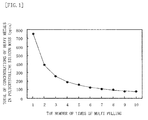
- Table 1 shows the result of theoretical calculation performed to determine the concentrations of the heavy metal impurities in a bulk of a polycrystalline silicon mass tolerable for keeping the respective concentrations of chromium, iron, nickel, copper, and cobalt in CZ single-crystal silicon not more than 0.05 ppta in the case where the CZ single-crystal silicon is grown by the multi pulling method.
- Figure 1 is a graph showing the result shown in Table 1. In the calculation, the solidified fraction in the final multi pulling was 0.9.
- the total of the concentrations of the heavy metal impurities in a bulk of a polycrystalline silicon mass tolerable for keeping the respective concentrations of chromium, iron, nickel, copper, and cobalt in the CZ single-crystal silicon not more than 0.05 ppta is 759 ppta.
- the total of the tolerable concentrations of heavy metal impurities reduces as the number of times of the multi pulling is increased.
- the CZ single-crystal silicon is grown by the multi pulling method using a raw material of a polycrystalline silicon mass in which the total of the concentrations of chromium, iron, nickel, copper, and cobalt detected from a polycrystalline silicon mass (the total of the concentrations of the heavy metal impurities detected from a bulk) is not more than 150 ppta, the crystal having no OSF can be obtained at the number of times of multi pulling of not more than 5. Moreover, defects at a deep level are hardly produced in the CZ single-crystal having such low concentrations of impurities, and the lifetime of the minority carriers are increased.
- the CZ single-crystal is also suitable for production of a silicon substrate for solar cells.
- the crystal having no OSF can be obtained at the number of times of multi pulling of not more than 7.
- the raw material may be a polycrystalline silicon mass in which the total of the concentrations of chromium, iron, nickel, copper, and cobalt detected from polycrystalline silicon is not more than 75 ppta.
- the concentrations of the heavy metal impurities in a polycrystalline silicon mass can be detected by an ICP-MS (Inductivity Coupled Plasma-Mass Spectrometry) method, for example.
- ICP-MS Inductivity Coupled Plasma-Mass Spectrometry
- a polycrystalline silicon piece as a sample to be analyzed is dissolved in a small amount of a mixed acid of a hydrogen fluoride solution and nitric acid, and evaporated to dryness.
- the residue is dissolved in 5% nitric acid to prepare an aqueous solution, and the concentrations of chromium, iron, nickel, copper, and cobalt in the aqueous solution are analyzed.
- Figure 2 is a schematic view showing an example of an embodiment of a polycrystalline silicon rod 100 used as a mother material for a polycrystalline silicon mass when the polycrystalline silicon mass is produced by the Siemens method.
- Figure 3 is a flowchart for describing an example of steps of producing a polycrystalline silicon mass according to the present invention.
- the polycrystalline silicon rod 100 has a first silicon core wire 31 and a second silicon core wire 32 disposed approximately in parallel to each other.
- the first silicon core wire 31 and the second silicon core wire 32 are connected by a silicon core wire 33 for connection.
- Polycrystalline silicon 10 is deposited on these core wires by a gaseous phase reaction, and formed.
- first silicon core wire 31 and one end of the second silicon core wire 32 are inserted into conductive holders 51 and 52 made of carbon, for example, respectively.
- the conductive holders 51 and 52 are fixed to metal electrodes 61 and 62 made of copper or stainless steel and provided within a reactor of a vapor deposition apparatus (not shown).
- the first silicon core wire 31 and the second silicon core wire 32 are disposed approximately in parallel to each other in the vertical direction.
- the silicon core wire 33 for connection is disposed between the other end of the first silicon core wire 31 and the other end of the second silicon core wire 32 to connect the first and second silicon core wires 31 and 32 (core installation step: S101).
- Anticorrosive stainless steel is used for the wall of the reactor in the vapor deposition apparatus.
- an atmosphere within the reactor is sequentially replaced with nitrogen and hydrogen, and heating of the first and second silicon core wires 31 and 32 and the silicon core wire 33 for connection is started in the hydrogen atmosphere.
- the first and second silicon core wires 31 and 32 and the silicon core wire 33 for connection are electrically conducted from the metal electrodes 61 and 62 through the conductive holders 51 and 52 and heated.
- a desired temperature for example, 900°C to 1100°C
- raw material gas such as trichlorosilane is fed into the growth furnace, and the polycrystalline silicon 10 is vapor deposited to form the polycrystalline silicon rod 100 (vapor deposition step: S102).
- the polycrystalline silicon 10 is grown to have a desired diameter (for example, 120 mm)
- feeding of the raw material gas is stopped, and the temperature within the reactor is reduced.
- the atmosphere within the reactor is replaced from hydrogen to nitrogen, and the reactor is opened to the atmosphere.
- the polycrystalline silicon rod 100 vapor deposited in the hydrogen atmosphere has a hydrogen-terminated (H 2 -terminated) surface
- the surface is likely to adsorb metal grains such as chromium, iron, nickel, copper, and cobalt particularly in the post steps such as the extraction step and the crushing step.
- the surface of the polycrystalline silicon rod 100 is covered with a bag-like member for preventing contamination by metals (S103), and the covered polycrystalline silicon rod 100 is extracted from the reactor.
- adhesion of iron powder produced from a crane or the like used for extraction or particles of chromium and nickel spread from the wall of the stainless steel reactor to the polycrystalline silicon rod 100 can be significantly suppressed.
- the polycrystalline silicon rod 100 by covering the polycrystalline silicon rod 100 with a bag having high impact resistance and being difficult to break, even if the polycrystalline silicon rod 100 is broken during the extraction step, the broken portion is held within the bag. For this reason, the polycrystalline silicon 10 can be prevented from falling on the baseplate or the electrodes and being contaminated by chromium, nickel, or copper. Examples of the bag for preventing contamination by metals that is difficult to break include polyethylene bags.
- the polycrystalline silicon rod 100 is disposed approximately horizontally, and the opening of the bag for preventing contamination by metals that covers the polycrystalline silicon rod 100 is sealed. Thereby, mixing of the metal grains from the opening into the bag and adhesion of the metal grains to the polycrystalline silicon rod 100 can be prevented.
- the total number of the polycrystalline silicon rods 100 is covered with the bags for preventing contamination by metals in advance, and the extraction step is started. Thereby, adhesion of the metals to the polycrystalline silicon rod 100 can be securely reduced.
- the polycrystalline silicon rod 100 is covered with the bag for preventing contamination by metals, and extracted by a crane or the like from the reactor (extraction step: S104).
- the bag for preventing contamination by metals covers the polycrystalline silicon rod 100 until the polycrystalline silicon rod 100 is fed to the crushing step.
- the polycrystalline silicon rod 100 extracted from the reactor is evacuated from the room installed with the vapor deposition apparatus as soon as possible, and stored in a clean room at a low level of environmental contamination. Thereby, the surface of the polycrystalline silicon rod 100 is kept as clean as possible. As described above, by sealing the opening of the bag for preventing contamination by metals, the polycrystalline silicon rod 100 can be kept much cleaner.
- a heat resistant stainless steel plate is used for the baseplate of the vapor deposition apparatus.
- the stainless steel plate is gradually corroded in a high temperature chlorine-containing atmosphere. If the stainless steel plate is corroded, the metal grains containing nickel and chromium are spread in the growth atmosphere. Moreover, copper or stainless steel is used for the metal electrode.
- the polycrystalline silicon rod 100 on the electrode side is closer to the baseplate and the metal electrode, and the possibility of the contamination by metals is higher. Further, in contamination of the surface, even if the polycrystalline silicon rod 100 is covered with the bag for preventing contamination by metals during the extraction step S104, the bag is opened on the electrode side of the polycrystalline silicon rod 100. For this reason, the total of the concentrations of chromium, iron, nickel, copper, and cobalt detected from a bulk is likely to be higher toward the electrode side of the polycrystalline silicon rod 100.
- removal of a predetermined range of a polycrystalline silicon portion from the electrode side end of the polycrystalline silicon rod 100 extracted to the outside of the reactor is effective to reduction in the concentrations of the impurities.
- Figure 4 is an example of a graph showing a relationship between the distance from the electrode side end of the polycrystalline silicon rod 100 to a portion thereof and the concentrations of the respective heavy metal impurities of chromium, iron, nickel, copper, and cobalt contained in the portion and the total of the concentrations, which is determined by the test by the present inventors.
- the total of the concentrations of chromium, iron, nickel, copper, and cobalt is 198 ppta in a portion located at a distance from the electrode side end of 50 mm, 112 ppta in a portion located at a distance from the electrode side end of 100 mm, and 54 ppta in a portion located at a distance from the electrode side end of 220 mm.
- the measured value of the total of the concentrations is determined by curve approximation: the total of the concentrations in a portion located at a distance from the electrode side end of 70 mm is 149 ppta, and the total of the concentrations in a portion located at a distance from the electrode side end of 155 mm is 74 ppta.
- the present invention comprises a removing step of removing at least 70 mm of a polycrystalline silicon portion from the electrode side end of the polycrystalline silicon rod 100 extracted to the outside of the reactor before the crushing step of the polycrystalline silicon rod 100 (S105).
- the polycrystalline silicon portion in which the total of the concentrations of chromium, iron, nickel, copper, and cobalt in a bulk is not less than 150 ppta can be removed.
- at least 155 mm of polycrystalline silicon portion from the electrode side end of the polycrystalline silicon rod may be removed.
- the polycrystalline silicon portion having the total of the concentrations of the impurities of not less than 75 ppta can be removed.
- region H having the high concentrations of the heavy metal impurities is removed before the crushing step.
- the region H having the high concentrations of the heavy metal impurities can be removed by cutting using a rotary blade, for example.
- the polycrystalline silicon rod 100 is crushed using a jaw crusher or a hammer to form polycrystalline silicon masses (crushing step: S106).
- a contact portion with polycrystalline silicon in the jaw crusher or the hammer is made of cemented carbide (WC-Co alloy) obtained by sintering tungsten carbide with a cobalt alloy.
- the metal particles containing chromium, iron, nickel, or copper adhering to the surface of the polycrystalline silicon rod 100 are moved to the surface of the polycrystalline silicon mass, and the cobalt particles from the WC-Co alloy also adhere to the surface of the polycrystalline silicon mass.
- the metal grains such as chromium, iron, nickel, copper, and cobalt adhering to the surface of the polycrystalline silicon mass are removed.
- Tungsten (W) has a very small segregation coefficient of 1.7 x 10 -8 , and substantially is not taken from the melt into the CZ single-crystal silicon. Accordingly, management of the amount of tungsten to be detected does not need to be as severe as that of the five kinds of metals.
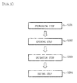
- FIG. 5 is a flowchart showing an example of a washing step.
- the polycrystalline silicon mass is placed in a basket for washing.
- the basket is swung in pure water to roughly remove polycrystalline silicon grains adhering to the surface of the polycrystalline silicon mass (prewashing step: S201).
- a natural oxide film formed on the surface of the polycrystalline silicon mass is removed by etching (S202).
- the washing liquid for example, a mixed solution of a hydrogen fluoride solution, a hydrogen peroxide solution, and water (FPM solution) or a mixed solution of a hydrogen fluoride solution and nitric acid (fluoronitric acid) can be used.
- FPM solution a mixed solution of a hydrogen fluoride solution, a hydrogen peroxide solution, and water
- fluoronitric acid fluoronitric acid
- the FPM solution removes the natural oxide film formed on the surface of the polycrystalline silicon mass by etching, and removes the metal grains in the natural oxide film or adhering onto the natural oxide film together with the natural oxide film by etching, but hardly etches the polycrystalline silicon itself. Accordingly, reduction in yield can be suppressed.
- fluoronitric acid can remove not only the natural oxide film formed on the surface of the polycrystalline silicon mass but also the polycrystalline silicon itself by etching, and it is effective to remove the metal grains adhering to depressions of the polycrystalline silicon mass, for example.
- An ability to remove the metal grains is higher as the amount of etching is larger. By etching not less than 20 ⁇ m, the metal grains adhering to the surface of the polycrystalline silicon mass can be sufficiently removed.
- the polycrystalline silicon masses are immersed in a rinsing bath, and rinsed with pure water. When necessary, a plurality of rinsing bathes is used.
- the polycrystalline silicon masses after the etching step were analyzed by the IPC-MS method.
- the total of the concentrations of chromium, iron, nickel, copper, and cobalt detected from a bulk was not more than 75 ppta.
- the surface of the polycrystalline silicon mass is once cleaned and the metal grains adhere to the surface of the polycrystalline silicon mass again later, the effect of washing is undesirably reduced. Accordingly, in the present invention, in the final step of the washing step, the surface of the polycrystalline silicon mass is subjected to oxidation treatment by ozone water to coat the polycrystalline silicon mass with a silicon oxide film. At this time, ozone water also decomposes and removes organic substances adhering to the surface of the polycrystalline silicon mass.
- the surface of the polycrystalline silicon mass is coated with a silicon oxide film, the surface of the polycrystalline silicon mass becomes inactive. Accordingly, the metal grains are difficult to adhere to the surface of the polycrystalline silicon mass again. Moreover, dirt referred to as a stain is difficult to occur. Further, even if the metal grains adhere, the metal grains adhere through the silicon oxide film to the polycrystalline silicon mass. For this reason, bond between the metal grains and the polycrystalline silicon is weak.
- the polycrystalline silicon mass is kept clean, in which the total of the concentrations of the five element metals is kept not more than 75 ppta.
- the polycrystalline silicon mass is immersed in ozone water, and the cleaned surface of the polycrystalline silicon mass is coated with a silicon oxide film (oxidation step: S203). Finally, the polycrystalline silicon mass is dried by clean warm air or in vacuum (drying step: S204). Thereby, the surface of the polycrystalline silicon mass is coated with a clean silicon oxide film, and the washing step is completed.
- the thus-obtained polycrystalline silicon mass having the total of the concentrations of chromium, iron, nickel, copper, and cobalt of not more than 75 ppta is used as the raw material.
- the CZ single-crystal silicon in which occurrence of OSFs and reduction in the lifetime of minority carriers are suppressed can be obtained even if at least 10 single-crystal silicon ingots are grown by the multi pulling method and pulled up in a single batch.
- a clean and high-purity polycrystalline silicon mass having a small content of chromium, iron, nickel, copper, and cobalt in total, which are heavy metal impurities that reduce the quality of single-crystal silicon, is provided.
Abstract
Description
- The present invention relates to a technique for producing a polycrystalline silicon mass, and more specifically, relates to a technique for producing a high purity polycrystalline silicon mass suitable for a raw material for growth of single-crystal silicon by a multi pulling method in particular.
- A Siemens method is known as a method for producing polycrystalline silicon used as a raw material for silicon single-crystal substrates. The Siemens method is a method in which a raw material gas containing chlorosilane is contacted with a heated silicon core wire, and polycrystalline silicon is vapor deposited on the surface of the silicon core wire by a CVD (Chemical Vapor Deposition) method.
- Usually, production of polycrystalline silicon by the Siemens method is performed according to the following steps, for example. First, two silicon core wires in the vertical direction and one silicon core wire in the horizontal direction are assembled into a II-shape (approximately inverted U-shaped) within a reactor of a vapor deposition apparatus, and the ends of the two core wires in the vertical direction are each fixed to metal electrodes through conductive holders (a core installation step).
- Next, while a current is conducted from the metal electrodes to heat the II-shaped silicon core wire in a hydrogen atmosphere, a raw material gas such as trichlorosilane is fed into the reactor, and polycrystalline silicon is vapor deposited on the core wire in an inverted U-shape. Thereby, a polycrystalline silicon rod having a desired diameter is obtained (a vapor deposition step).
- After the inside of the reactor is cooled, the polycrystalline silicon rod is extracted from the reactor using a crane or the like (an extraction step).
- The entire polycrystalline silicon rod extracted to the outside of the reactor is crushed using a crusher or a hammer to prepare polycrystalline silicon masses having a size suitable for feeding to a quartz crucible used for growth of a single-crystal silicon ingot by the CZ (Czochralski) method (a crushing step).
- Finally, the polycrystalline silicon masses are washed, and foreign substances and impurities adhering to the surfaces of the polycrystalline silicon masses are removed to obtain clean polycrystalline silicon (a washing step).
- Recently, as integration density of semiconductor devices as final products is increased, high purity of CZ single-crystal silicon that is a material of a substrate for highly integrated semiconductor devices has been severely demanded. Inevitably, higher purity of the polycrystalline silicon mass used as the raw material for the CZ single-crystal silicon has been more severely demanded.
- If the polycrystalline silicon mass has insufficient purity and contains heavy metals such as iron and copper, these impurities are molten into a silicon melt, and taken into the CZ single-crystal silicon to be grown, inhibiting higher purity. Such impurities taken from the polycrystalline silicon mass into the silicon melt are particularly serious in the case where the CZ single-crystal silicon is grown by a multi pulling method.
- The multi pulling method is a method for crystal growth in which in a single batch, after a single-crystal silicon ingot is pulled up, the polycrystalline silicon masses are newly added into the remaining silicon melt without turning off the power supply of the heater that heats a quartz crucible, thereby to pull up another single-crystal silicon ingot; the procedure is repeated to obtain a plurality of single-crystal silicon ingots. The method is devised for the purpose of improvement in productivity of the CZ single-crystal silicon and reduction in production cost.
- Usually, heavy metal elements such as iron and copper have a segregation coefficient k greatly less than 1 as an index indicating how easily the element is taken from the silicon melt (liquid phase) into the silicon crystal (solid phase) at a solid-liquid interface. Accordingly, these heavy metal elements are likely to remain in the silicon melt.
- Accordingly, in the case where the CZ single-crystal silicon ingot is grown by the multi pulling method, as the number of the single-crystal silicon ingot to be pulled up in one batch is increased and as the single-crystal silicon ingot is pulled up later in the one batch, the impurities having a segregation coefficient k less than 1 are grown from the silicon melt having a high concentration of "condensed" impurities. For this, the concentration of the impurities taken into the single-crystal silicon is gradually increased.
- The heavy metal impurities in the single-crystal silicon cause OSFs (Oxidation induced Stacking Faults) and a reduced lifetime of minority carriers to reduce the quality of the CZ single-crystal silicon. For this reason, it is important to reduce the amount of the heavy metal impurities to be taken from the polycrystalline silicon mass as the raw material for the CZ single-crystal silicon into the crucible (the silicon melt) as much as possible, and the polycrystalline silicon mass having sufficiently high purity is needed.
- In order to provide higher purity of the polycrystalline silicon mass as the raw material used for growth of single-crystal silicon, a variety of washing methods has been proposed. For example, Japanese Patent Laid-Open No.
4-357106 - Japanese Patent Laid-Open No.
8-67511 - Japanese Patent Laid-Open No.
11-168076 - Japanese Patent Laid-Open No.
2000-128692 Patent Literature 2 above, because polycrystalline silicon is finally washed by hydrofluoric acid, the surfaces of the polycrystalline silicon masses are chemically activated, and likely to be susceptible to contamination from an environment. - Japanese Patent Laid-Open No.
5-4811 - Unfortunately, the method is a washing method as part of a method for growing single-crystal silicon, and needs to be performed immediately before polycrystalline silicon masses are charged into a quartz crucible for pulling up CZ single-crystal.
-
- Patent Literature 1: Japanese Patent Laid-Open No.
4-357106 - Patent Literature 2: Japanese Patent Laid-Open No.
8-67511 - Patent Literature 3: Japanese Patent Laid-Open No.
11-168076 - Patent Literature 4: Japanese Patent Laid-Open No.
2000-128692 - Patent Literature 5: Japanese Patent Laid-Open No.
5-4811 -
- Non Patent Literature 1: "Shirikon no Kagaku (Science of Silicon)," p. 100, Table 5 (Realize Science & Engineering Center Co., Ltd., 1996)
- These related arts relate to the washing method for cleaning the surface of the polycrystalline silicon mass. The heavy metal impurities taken from the polycrystalline silicon mass into the crucible (silicon melt), however, are contained not only in the surface of the polycrystalline silicon mass but also in the entire bulk of the polycrystalline silicon mass.
- In the step of producing the polycrystalline silicon mass, many sources to produce the heavy metal impurities that may be taken into the bulk or adhering to the surface of the polycrystalline silicon mass exist. For example, a heat resistant stainless steel plate is used for the wall and baseplate of the reactor in the vapor deposition apparatus, and if the stainless steel plate is corroded, metal grains containing nickel and chromium are spread in the growth atmosphere. Moreover, copper or stainless steel is used for the metal electrode. For this reason, nickel, chromium, and copper are likely to be taken into the bulk of polycrystalline silicon.
- After vapor deposition is completed, by use of a crane to extract the polycrystalline silicon rod, iron powder is produced from the crane.
- In the case where the polycrystalline silicon rod is crushed using a jaw crusher, a roll crusher, or a hammer, cemented carbide used for these crushing means contacts with polycrystalline silicon. As the cemented carbide, a material prepared by sintering tungsten carbide with a cobalt alloy is used, and iron and cobalt are likely to adhere to the surface of the polycrystalline silicon mass.
- Further, after the deposition reaction of polycrystalline silicon is completed, when the reactor is opened to the work atmosphere, metal grains containing nickel, chromium, and copper are spread from the inside of the reactor to the work atmosphere, and these metal grains are likely to adhere to the surface of the polycrystalline silicon mass.
- The present invention has been made in consideration of the problems above, and an object of the present invention is to provide a clean and high-purity polycrystalline silicon mass having a small content of chromium, iron, nickel, copper, and cobalt in total, which are heavy metal impurities that reduce the quality of single-crystal silicon.
- In order to solve the problems above, in a polycrystalline silicon mass according to the present invention, a total of concentrations of impurities of chromium, iron, nickel, copper, and cobalt detected from a bulk is not more than 150 ppta. Preferably, the total of the concentrations of the impurities is not more than 100 ppta. More preferably, the total of the concentrations of the impurities is not more than 75 ppta.
- The concentrations of the impurities can be determined by an inductively coupled plasma mass spectrometry (ICP-MS) method. Preferably, the surface of the polycrystalline silicon mass according to the present invention is coated with a silicon oxide film.
- Moreover, the polycrystalline silicon mass according to the present invention is a polycrystalline silicon mass for multi pulling in which up to 10 single-crystal silicon ingots are pulled up by a CZ method in one batch, wherein a total of concentrations of impurities of chromium, iron, nickel, copper, and cobalt detected from a bulk is not more than 75 ppta, and a surface of the polycrystalline silicon mass is coated with a silicon oxide film.
- A process for producing a polycrystalline silicon mass according to the present invention comprises: a vapor deposition step of depositing silicon on a core wire to grow a polycrystalline silicon rod, one end of the core wire being connected to a first electrode and the other end thereof being connected to a second electrode; an extraction step of extracting the polycrystalline silicon rod to an outside of a reactor; and a crushing step of forming the polycrystalline silicon rod into polycrystalline silicon masses, the process further comprising a removing step of removing at least 70 mm of a polycrystalline silicon portion from an electrode side end of the polycrystalline silicon rod extracted to the outside of the reactor before the crushing step.
- Preferably, at least 155 mm of the polycrystalline silicon portion from the electrode side end is removed in the removing step.
- Moreover, preferably, a surface of the polycrystalline silicon rod is covered with a bag-like member and extracted to the outside of the reactor in the extraction step. More preferably, after the polycrystalline silicon rod is extracted to the outside of the reactor, an opening of the bag-like member that covers the surface of the polycrystalline silicon rod is sealed. The bag-like member is a polyethylene bag, for example.
- The process for producing a polycrystalline silicon mass according to the present invention may comprise a washing step as a post step of the crushing step, wherein the surface of the polycrystalline silicon mass is subjected to oxidation treatment using ozone water to coat the surface of the polycrystalline silicon mass with a silicon oxide film, and the washing step is completed in the state where the surface of the polycrystalline silicon mass is coated with the silicon oxide film.
- The present invention comprises a removing step of removing at least 70 mm of a polycrystalline silicon portion from an electrode side end of a polycrystalline silicon rod obtained by the Siemens method. Thereby, the polycrystalline silicon portion in which the total of the chromium, iron, nickel, copper, and cobalt concentrations in a bulk is not less than 150 ppta is removed, and a clean and high-purity polycrystalline silicon mass having a small content of chromium, iron, nickel, copper, and cobalt in total, which are heavy metal impurities that reduce the quality of single-crystal silicon can be provided.
-
- [
Figure 1] Figure 1 is a graph showing the result of theoretical calculation performed to determine the total of the concentrations of the heavy metal impurities in a polycrystalline silicon mass grown by the multi pulling method, which is tolerable for keeping the respective concentrations of chromium, iron, nickel, copper, and cobalt in CZ single-crystal silicon not more than 0.05 ppta. - [
Figure 2] Figure 2 is a schematic view showing an example of an embodiment of a polycrystalline silicon rod used as a mother material for a polycrystalline silicon mass when the polycrystalline silicon mass is produced by the Siemens method. - [
Figure 3] Figure 3 is a flowchart for describing an example of steps of producing a polycrystalline silicon mass according to the present invention. - [
Figure 4] Figure 4 is an example of a graph showing a relationship between the distance from the electrode side end of a polycrystalline silicon rod to a portion of the polycrystalline silicon rod and the concentrations of the heavy metal impurities of chromium, iron, nickel, copper, and cobalt contained in the portion and the total of the concentrations. - [
Figure 5] Figure 5 is a flowchart showing an example of a washing step. - Hereinafter, with reference to the drawings, an embodiment according to the present invention will be described.
- It is known that heavy metal impurities in CZ single-crystal silicon cause oxidation induced stacking faults (OSFs) and a reduced lifetime of minority carriers. Specifically, if the concentrations of chromium, iron, nickel, and copper in the CZ single-crystal silicon each are not more than 0.05 ppta, occurrence of OSFs is suppressed ("Shirikon no Kagaku (Science of Silicon)," p. 100, Table 5, 1996, published by Realize Science & Engineering Center Co., Ltd.: Non Patent Literature 1). Moreover, if the concentrations of chromium, iron, nickel, copper, and cobalt each are not more than 0.05 ppta, no substantial reduction in the lifetime of minority carriers is found. Accordingly, in order to obtain high quality CZ single-crystal silicon in which the OSFs hardly occur and the lifetime of minority carriers is long, the concentrations of chromium, iron, nickel, copper, and cobalt in CZ single-crystal silicon each need to be not more than 0.05 ppta.
- The segregation coefficients of the respective heavy metal elements are already known, and the concentrations of the heavy metal impurities in a bulk of a polycrystalline silicon mass, which is tolerable for keeping the concentrations of impurities in the CZ single-crystal silicon not more than the value mentioned above, can be theoretically determined.
- Table 1 shows the result of theoretical calculation performed to determine the concentrations of the heavy metal impurities in a bulk of a polycrystalline silicon mass tolerable for keeping the respective concentrations of chromium, iron, nickel, copper, and cobalt in CZ single-crystal silicon not more than 0.05 ppta in the case where the CZ single-crystal silicon is grown by the multi pulling method.
Figure 1 is a graph showing the result shown in Table 1. In the calculation, the solidified fraction in the final multi pulling was 0.9. - As shown in Table 1, in the case where the number of times of multi pulling, n is 1 (actually, no multi pulling is performed), the total of the concentrations of the heavy metal impurities in a bulk of a polycrystalline silicon mass tolerable for keeping the respective concentrations of chromium, iron, nickel, copper, and cobalt in the CZ single-crystal silicon not more than 0.05 ppta is 759 ppta. The total of the tolerable concentrations of heavy metal impurities reduces as the number of times of the multi pulling is increased. At n = 5, the concentrations of the heavy metal impurities is approximately 150 ppta (152 ppta), and at n = 10, the concentrations of the heavy metal impurities is approximately 75 ppta (76 ppta).
-
[Table 1] Element Segregation coefficient Solidified fraction The number of times of multi pulling and tolerable concentrations of impurities in polycrystalline silicon mass (ppta) 1 2 3 4 5 6 7 8 9 10 Cr 1.10E-05 0.9 465 227 152 114 91 76 65 57 51 45 Fe 8.00E-05 0.9 63 31 21 16 13 10 9 8 7 6 Ni 3.00E-05 0.9 167 83 56 42 33 28 24 21 19 17 Cu 4.00E-04 0.9 13 6 4 3 3 2 2 2 1 1 Co 8.00E-05 0.9 63 31 21 16 13 10 9 8 7 6 Total - - 759 379 253 190 152 126 108 95 84 76 - Namely, if the CZ single-crystal silicon is grown by the multi pulling method using a raw material of a polycrystalline silicon mass in which the total of the concentrations of chromium, iron, nickel, copper, and cobalt detected from a polycrystalline silicon mass (the total of the concentrations of the heavy metal impurities detected from a bulk) is not more than 150 ppta, the crystal having no OSF can be obtained at the number of times of multi pulling of not more than 5. Moreover, defects at a deep level are hardly produced in the CZ single-crystal having such low concentrations of impurities, and the lifetime of the minority carriers are increased. The CZ single-crystal is also suitable for production of a silicon substrate for solar cells.
- Moreover, if the CZ single-crystal silicon is grown by the multi pulling method using a raw material of a polycrystalline silicon mass in which the total of the concentrations of chromium, iron, nickel, copper, and cobalt detected from a polycrystalline silicon mass is not more than 100 ppta, the crystal having no OSF can be obtained at the number of times of multi pulling of not more than 7.
- Further, in order to obtain the crystal having no OSF at the number of times of multi pulling of not more than 10, the raw material may be a polycrystalline silicon mass in which the total of the concentrations of chromium, iron, nickel, copper, and cobalt detected from polycrystalline silicon is not more than 75 ppta.
- The concentrations of the heavy metal impurities in a polycrystalline silicon mass can be detected by an ICP-MS (Inductivity Coupled Plasma-Mass Spectrometry) method, for example. In the ICP-MS method, a polycrystalline silicon piece as a sample to be analyzed is dissolved in a small amount of a mixed acid of a hydrogen fluoride solution and nitric acid, and evaporated to dryness. The residue is dissolved in 5% nitric acid to prepare an aqueous solution, and the concentrations of chromium, iron, nickel, copper, and cobalt in the aqueous solution are analyzed.
-
Figure 2 is a schematic view showing an example of an embodiment of apolycrystalline silicon rod 100 used as a mother material for a polycrystalline silicon mass when the polycrystalline silicon mass is produced by the Siemens method.Figure 3 is a flowchart for describing an example of steps of producing a polycrystalline silicon mass according to the present invention. - The
polycrystalline silicon rod 100 has a firstsilicon core wire 31 and a secondsilicon core wire 32 disposed approximately in parallel to each other. The firstsilicon core wire 31 and the secondsilicon core wire 32 are connected by asilicon core wire 33 for connection.Polycrystalline silicon 10 is deposited on these core wires by a gaseous phase reaction, and formed. - One end of the first
silicon core wire 31 and one end of the secondsilicon core wire 32 are inserted intoconductive holders conductive holders metal electrodes silicon core wire 31 and the secondsilicon core wire 32 are disposed approximately in parallel to each other in the vertical direction. Thesilicon core wire 33 for connection is disposed between the other end of the firstsilicon core wire 31 and the other end of the secondsilicon core wire 32 to connect the first and secondsilicon core wires 31 and 32 (core installation step: S101). Anticorrosive stainless steel is used for the wall of the reactor in the vapor deposition apparatus. - After the core installation step is completed, an atmosphere within the reactor is sequentially replaced with nitrogen and hydrogen, and heating of the first and second
silicon core wires silicon core wire 33 for connection is started in the hydrogen atmosphere. The first and secondsilicon core wires silicon core wire 33 for connection are electrically conducted from themetal electrodes conductive holders polycrystalline silicon 10 is vapor deposited to form the polycrystalline silicon rod 100 (vapor deposition step: S102). - After the
polycrystalline silicon 10 is grown to have a desired diameter (for example, 120 mm), feeding of the raw material gas is stopped, and the temperature within the reactor is reduced. The atmosphere within the reactor is replaced from hydrogen to nitrogen, and the reactor is opened to the atmosphere. - Because the
polycrystalline silicon rod 100 vapor deposited in the hydrogen atmosphere has a hydrogen-terminated (H2-terminated) surface, the surface is likely to adsorb metal grains such as chromium, iron, nickel, copper, and cobalt particularly in the post steps such as the extraction step and the crushing step. - For this reason, before the
polycrystalline silicon rod 100 formed into an inverted U-shape is extracted, the surface of thepolycrystalline silicon rod 100 is covered with a bag-like member for preventing contamination by metals (S103), and the coveredpolycrystalline silicon rod 100 is extracted from the reactor. Thereby, adhesion of iron powder produced from a crane or the like used for extraction or particles of chromium and nickel spread from the wall of the stainless steel reactor to thepolycrystalline silicon rod 100 can be significantly suppressed. - Additionally, by covering the
polycrystalline silicon rod 100 with a bag having high impact resistance and being difficult to break, even if thepolycrystalline silicon rod 100 is broken during the extraction step, the broken portion is held within the bag. For this reason, thepolycrystalline silicon 10 can be prevented from falling on the baseplate or the electrodes and being contaminated by chromium, nickel, or copper. Examples of the bag for preventing contamination by metals that is difficult to break include polyethylene bags. - Moreover, after extraction, the
polycrystalline silicon rod 100 is disposed approximately horizontally, and the opening of the bag for preventing contamination by metals that covers thepolycrystalline silicon rod 100 is sealed. Thereby, mixing of the metal grains from the opening into the bag and adhesion of the metal grains to thepolycrystalline silicon rod 100 can be prevented. - In the case where a plurality of
polycrystalline silicon rods 100 exist within the reactor, the total number of thepolycrystalline silicon rods 100 is covered with the bags for preventing contamination by metals in advance, and the extraction step is started. Thereby, adhesion of the metals to thepolycrystalline silicon rod 100 can be securely reduced. - The
polycrystalline silicon rod 100 is covered with the bag for preventing contamination by metals, and extracted by a crane or the like from the reactor (extraction step: S104). The bag for preventing contamination by metals covers thepolycrystalline silicon rod 100 until thepolycrystalline silicon rod 100 is fed to the crushing step. - The
polycrystalline silicon rod 100 extracted from the reactor is evacuated from the room installed with the vapor deposition apparatus as soon as possible, and stored in a clean room at a low level of environmental contamination. Thereby, the surface of thepolycrystalline silicon rod 100 is kept as clean as possible. As described above, by sealing the opening of the bag for preventing contamination by metals, thepolycrystalline silicon rod 100 can be kept much cleaner. - A heat resistant stainless steel plate is used for the baseplate of the vapor deposition apparatus. The stainless steel plate is gradually corroded in a high temperature chlorine-containing atmosphere. If the stainless steel plate is corroded, the metal grains containing nickel and chromium are spread in the growth atmosphere. Moreover, copper or stainless steel is used for the metal electrode. The
polycrystalline silicon rod 100 on the electrode side is closer to the baseplate and the metal electrode, and the possibility of the contamination by metals is higher. Further, in contamination of the surface, even if thepolycrystalline silicon rod 100 is covered with the bag for preventing contamination by metals during the extraction step S104, the bag is opened on the electrode side of thepolycrystalline silicon rod 100. For this reason, the total of the concentrations of chromium, iron, nickel, copper, and cobalt detected from a bulk is likely to be higher toward the electrode side of thepolycrystalline silicon rod 100. - Accordingly, before the crushing step, removal of a predetermined range of a polycrystalline silicon portion from the electrode side end of the
polycrystalline silicon rod 100 extracted to the outside of the reactor is effective to reduction in the concentrations of the impurities. -
Figure 4 is an example of a graph showing a relationship between the distance from the electrode side end of thepolycrystalline silicon rod 100 to a portion thereof and the concentrations of the respective heavy metal impurities of chromium, iron, nickel, copper, and cobalt contained in the portion and the total of the concentrations, which is determined by the test by the present inventors. The total of the concentrations of chromium, iron, nickel, copper, and cobalt is 198 ppta in a portion located at a distance from the electrode side end of 50 mm, 112 ppta in a portion located at a distance from the electrode side end of 100 mm, and 54 ppta in a portion located at a distance from the electrode side end of 220 mm. The measured value of the total of the concentrations is determined by curve approximation: the total of the concentrations in a portion located at a distance from the electrode side end of 70 mm is 149 ppta, and the total of the concentrations in a portion located at a distance from the electrode side end of 155 mm is 74 ppta. - Accordingly, the present invention comprises a removing step of removing at least 70 mm of a polycrystalline silicon portion from the electrode side end of the
polycrystalline silicon rod 100 extracted to the outside of the reactor before the crushing step of the polycrystalline silicon rod 100 (S105). Thereby, the polycrystalline silicon portion in which the total of the concentrations of chromium, iron, nickel, copper, and cobalt in a bulk is not less than 150 ppta can be removed. In order to obtain a polycrystalline silicon mass having a lower concentration of the impurities, at least 155 mm of polycrystalline silicon portion from the electrode side end of the polycrystalline silicon rod may be removed. Thereby, the polycrystalline silicon portion having the total of the concentrations of the impurities of not less than 75 ppta can be removed. - Once the
polycrystalline silicon rod 100 is crushed, the polycrystalline silicon masses are mixed. For this reason, it is difficult to discriminate a region H having the high concentrations of the heavy metal impurities from other regions. Moreover, during crushing, the metal grains may be spread from the region H having the high concentrations of the heavy metal impurities to other regions. For this reason, desirably, region H having the high concentrations of the heavy metal impurities is removed before the crushing step. The region H having the high concentrations of the heavy metal impurities can be removed by cutting using a rotary blade, for example. - Subsequently, the
polycrystalline silicon rod 100 is crushed using a jaw crusher or a hammer to form polycrystalline silicon masses (crushing step: S106). Preferably, a contact portion with polycrystalline silicon in the jaw crusher or the hammer is made of cemented carbide (WC-Co alloy) obtained by sintering tungsten carbide with a cobalt alloy. - In the crushing step, the metal particles containing chromium, iron, nickel, or copper adhering to the surface of the
polycrystalline silicon rod 100 are moved to the surface of the polycrystalline silicon mass, and the cobalt particles from the WC-Co alloy also adhere to the surface of the polycrystalline silicon mass. Then, in the next washing step (S107), the metal grains such as chromium, iron, nickel, copper, and cobalt adhering to the surface of the polycrystalline silicon mass are removed. - Tungsten (W) has a very small segregation coefficient of 1.7 x 10⁻⁸, and substantially is not taken from the melt into the CZ single-crystal silicon. Accordingly, management of the amount of tungsten to be detected does not need to be as severe as that of the five kinds of metals.
-
Figure 5 is a flowchart showing an example of a washing step. First, the polycrystalline silicon mass is placed in a basket for washing. The basket is swung in pure water to roughly remove polycrystalline silicon grains adhering to the surface of the polycrystalline silicon mass (prewashing step: S201). - Next, using a known washing liquid, a natural oxide film formed on the surface of the polycrystalline silicon mass is removed by etching (S202). As the washing liquid, for example, a mixed solution of a hydrogen fluoride solution, a hydrogen peroxide solution, and water (FPM solution) or a mixed solution of a hydrogen fluoride solution and nitric acid (fluoronitric acid) can be used. In the present Example, the polycrystalline silicon masses are immersed in a bath containing a first chemical solution prepared by mixing a hydrogen fluoride solution, a hydrogen peroxide solution and water, and the natural oxide film formed on the surfaces of the polycrystalline silicon masses is removed by etching while the polycrystalline silicon masses are swung.
- The FPM solution removes the natural oxide film formed on the surface of the polycrystalline silicon mass by etching, and removes the metal grains in the natural oxide film or adhering onto the natural oxide film together with the natural oxide film by etching, but hardly etches the polycrystalline silicon itself. Accordingly, reduction in yield can be suppressed.
- Moreover, fluoronitric acid can remove not only the natural oxide film formed on the surface of the polycrystalline silicon mass but also the polycrystalline silicon itself by etching, and it is effective to remove the metal grains adhering to depressions of the polycrystalline silicon mass, for example. An ability to remove the metal grains is higher as the amount of etching is larger. By etching not less than 20 µm, the metal grains adhering to the surface of the polycrystalline silicon mass can be sufficiently removed.
- After the etching step is completed, the polycrystalline silicon masses are immersed in a rinsing bath, and rinsed with pure water. When necessary, a plurality of rinsing bathes is used.
- The polycrystalline silicon masses after the etching step were analyzed by the IPC-MS method. As a result, in each of the masses analyzed, the total of the concentrations of chromium, iron, nickel, copper, and cobalt detected from a bulk was not more than 75 ppta.
- If the surface of the polycrystalline silicon mass is once cleaned and the metal grains adhere to the surface of the polycrystalline silicon mass again later, the effect of washing is undesirably reduced. Accordingly, in the present invention, in the final step of the washing step, the surface of the polycrystalline silicon mass is subjected to oxidation treatment by ozone water to coat the polycrystalline silicon mass with a silicon oxide film. At this time, ozone water also decomposes and removes organic substances adhering to the surface of the polycrystalline silicon mass.
- If the surface of the polycrystalline silicon mass is coated with a silicon oxide film, the surface of the polycrystalline silicon mass becomes inactive. Accordingly, the metal grains are difficult to adhere to the surface of the polycrystalline silicon mass again. Moreover, dirt referred to as a stain is difficult to occur. Further, even if the metal grains adhere, the metal grains adhere through the silicon oxide film to the polycrystalline silicon mass. For this reason, bond between the metal grains and the polycrystalline silicon is weak. The polycrystalline silicon mass is kept clean, in which the total of the concentrations of the five element metals is kept not more than 75 ppta.
- In the present Example, the polycrystalline silicon mass is immersed in ozone water, and the cleaned surface of the polycrystalline silicon mass is coated with a silicon oxide film (oxidation step: S203). Finally, the polycrystalline silicon mass is dried by clean warm air or in vacuum (drying step: S204). Thereby, the surface of the polycrystalline silicon mass is coated with a clean silicon oxide film, and the washing step is completed.
- The thus-obtained polycrystalline silicon mass having the total of the concentrations of chromium, iron, nickel, copper, and cobalt of not more than 75 ppta is used as the raw material. Thereby, the CZ single-crystal silicon in which occurrence of OSFs and reduction in the lifetime of minority carriers are suppressed can be obtained even if at least 10 single-crystal silicon ingots are grown by the multi pulling method and pulled up in a single batch.
- According to the present invention, a clean and high-purity polycrystalline silicon mass having a small content of chromium, iron, nickel, copper, and cobalt in total, which are heavy metal impurities that reduce the quality of single-crystal silicon, is provided.
-
- 10
- Polycrystalline silicon
- 31
- First silicon core wire
- 32
- Second silicon core wire
- 33
- Silicon core wire for connection
- 51, 52
- Conductive holder
- 61, 62
- Metal electrode
- 100
- Polycrystalline silicon rod
- H
- Region having high concentrations of heavy metal impurities
Claims (12)
- A polycrystalline silicon mass, wherein a total of concentrations of chromium, iron, nickel, copper, and cobalt impurities detected from a bulk is not more than 150 ppta.
- The polycrystalline silicon mass according to claim 1, wherein the total of the concentrations of the impurities is not more than 100 ppta.
- The polycrystalline silicon mass according to claim 2, wherein the total of the concentrations of the impurities is not more than 75 ppta.
- The polycrystalline silicon mass according to any one of claims 1 to 3, wherein the concentrations of impurities are an analyzed value by an inductively coupled plasma mass spectrometry (ICP-MS) method.
- The polycrystalline silicon mass according to any one of claims 1 to 3, wherein the surface of the polycrystalline silicon mass is coated with a silicon oxide film.
- A polycrystalline silicon mass for multi pulling in which up to 10 single-crystal silicon ingots are pulled up by a CZ method in one batch, wherein
a total of concentrations of chromium, iron, nickel, copper, and cobalt impurities detected from a bulk is not more than 75 ppta, and a surface of the polycrystalline silicon mass is coated with a silicon oxide film. - A process for producing a polycrystalline silicon mass comprising: a vapor deposition step of depositing silicon on a core wire to grow a polycrystalline silicon rod, one end of the core wire being connected to a first electrode and the other end thereof being connected to a second electrode; an extraction step of extracting the polycrystalline silicon rod to an outside of a reactor; and a crushing step of forming the polycrystalline silicon rod into polycrystalline silicon masses,
the process further comprising a removing step of removing at least 70 mm of a polycrystalline silicon portion from an electrode side end of the polycrystalline silicon rod extracted to the outside of the reactor before the crushing step. - The process for producing a polycrystalline silicon mass according to claim 7, wherein at least 155 mm of the polycrystalline silicon portion from the electrode side end is removed in the removing step.
- The process for producing a polycrystalline silicon mass according to claim 7 or 8, wherein a surface of the polycrystalline silicon rod is covered with a bag-like member and extracted to the outside of the reactor in the extraction step.
- The process for producing a polycrystalline silicon mass according to claim 9, wherein an opening of the bag-like member that covers the surface of the polycrystalline silicon rod is sealed after the polycrystalline silicon rod is extracted to the outside of the reactor.
- The process for producing a polycrystalline silicon mass according to claim 9, wherein the bag-like member is a polyethylene bag.
- The process for producing a polycrystalline silicon mass according to claim 7 or 8 comprising a washing step as a post step of the crushing step, wherein
the surface of the polycrystalline silicon mass is subjected to oxidation treatment using ozone water to coat the surface of the polycrystalline silicon mass with a silicon oxide film, and the washing step is completed in the state where the surface of the polycrystalline silicon mass is coated with the silicon oxide film.
Applications Claiming Priority (2)
| Application Number | Priority Date | Filing Date | Title |
|---|---|---|---|
| JP2009214519A JP5751748B2 (en) | 2009-09-16 | 2009-09-16 | Polycrystalline silicon lump group and method for producing polycrystalline silicon lump group |
| PCT/JP2010/004668 WO2011033712A1 (en) | 2009-09-16 | 2010-07-21 | Polycrystalline silicon mass and process for producing polycrystalline silicon mass |
Publications (3)
| Publication Number | Publication Date |
|---|---|
| EP2479142A1 true EP2479142A1 (en) | 2012-07-25 |
| EP2479142A4 EP2479142A4 (en) | 2014-07-02 |
| EP2479142B1 EP2479142B1 (en) | 2017-05-31 |
Family
ID=43758330
Family Applications (1)
| Application Number | Title | Priority Date | Filing Date |
|---|---|---|---|
| EP10816827.9A Active EP2479142B1 (en) | 2009-09-16 | 2010-07-21 | Process for producing polycrystalline silicon mass |
Country Status (6)
| Country | Link |
|---|---|
| US (2) | US20120175613A1 (en) |
| EP (1) | EP2479142B1 (en) |
| JP (1) | JP5751748B2 (en) |
| CN (1) | CN102498064B (en) |
| AU (1) | AU2010296773B2 (en) |
| WO (1) | WO2011033712A1 (en) |
Cited By (6)
| Publication number | Priority date | Publication date | Assignee | Title |
|---|---|---|---|---|
| WO2013092337A1 (en) * | 2011-12-21 | 2013-06-27 | Wacker Chemie Ag | Polycrystalline silicon rod and method for producing polysilicon |
| DE102013207251A1 (en) | 2013-04-22 | 2014-10-23 | Wacker Chemie Ag | Process for producing polycrystalline silicon |
| WO2015062880A1 (en) * | 2013-10-28 | 2015-05-07 | Wacker Chemie Ag | Process for producing polycrystalline silicon |
| DE102014201096A1 (en) | 2014-01-22 | 2015-07-23 | Wacker Chemie Ag | Process for producing polycrystalline silicon |
| KR20170015384A (en) * | 2014-06-03 | 2017-02-08 | 신에쓰 가가꾸 고교 가부시끼가이샤 | Method for producing polycrystalline silicon rod, polycrystalline silicon rod, and polycrystalline silicon mass |
| EP3578514A4 (en) * | 2017-03-08 | 2020-10-07 | Tokuyama Corporation | Method for producing polycrystalline silicon processed article |
Families Citing this family (25)
| Publication number | Priority date | Publication date | Assignee | Title |
|---|---|---|---|---|
| JP5751748B2 (en) * | 2009-09-16 | 2015-07-22 | 信越化学工業株式会社 | Polycrystalline silicon lump group and method for producing polycrystalline silicon lump group |
| JP2012224499A (en) * | 2011-04-19 | 2012-11-15 | Shin-Etsu Chemical Co Ltd | Method for producing silicon core wire |
| DE102012200994A1 (en) * | 2012-01-24 | 2013-07-25 | Wacker Chemie Ag | Method for determining surface contamination of polycrystalline silicon |
| JP5828795B2 (en) | 2012-04-04 | 2015-12-09 | 信越化学工業株式会社 | Method for evaluating degree of crystal orientation of polycrystalline silicon, method for selecting polycrystalline silicon rod, and method for producing single crystal silicon |
| JP2014001096A (en) * | 2012-06-18 | 2014-01-09 | Shin Etsu Chem Co Ltd | Polycrystalline silicon crystal orientation degree evaluation method, polycrystalline silicon rod selection method, polycrystalline silicon rod, polycrystalline silicon ingot, and polycrystalline silicon fabrication method |
| DE102012213869A1 (en) * | 2012-08-06 | 2014-02-06 | Wacker Chemie Ag | Polycrystalline silicon fragments and process for their preparation |
| EP2943974B1 (en) * | 2013-01-08 | 2021-01-13 | SK Siltron Co., Ltd. | Method of detecting defects in silicon single crystal wafer |
| DE102013206339A1 (en) * | 2013-04-10 | 2014-10-16 | Wacker Chemie Ag | Apparatus and method for removing polycrystalline silicon rods from a reactor |
| DE102013206436A1 (en) | 2013-04-11 | 2014-10-16 | Wacker Chemie Ag | Cleaning of CVD production rooms |
| JP5947248B2 (en) * | 2013-06-21 | 2016-07-06 | 信越化学工業株式会社 | Selection method of polycrystalline silicon rod |
| JP5923463B2 (en) * | 2013-06-26 | 2016-05-24 | 信越化学工業株式会社 | Method for evaluating crystal grain size distribution of polycrystalline silicon, method for selecting polycrystalline silicon rod, polycrystalline silicon rod, polycrystalline silicon lump, and method for producing single crystalline silicon |
| JP5984758B2 (en) * | 2013-07-31 | 2016-09-06 | 信越化学工業株式会社 | How to handle silicon core wire |
| DE102013219070A1 (en) | 2013-09-23 | 2015-03-26 | Wacker Chemie Ag | Process for producing polycrystalline silicon |
| DE102014200058A1 (en) * | 2014-01-07 | 2015-07-09 | Wacker Chemie Ag | Device for picking up and transporting a silicon rod and method for producing polycrystalline silicon |
| DE102014201893A1 (en) * | 2014-02-03 | 2015-08-06 | Wacker Chemie Ag | Process for producing polycrystalline silicon |
| JP2015202999A (en) * | 2014-04-16 | 2015-11-16 | 信越化学工業株式会社 | Silicon crystal cleaning method and polycrystal silicon lump grinding method |
| JP6418778B2 (en) | 2014-05-07 | 2018-11-07 | 信越化学工業株式会社 | Polycrystalline silicon rod, method for producing polycrystalline silicon rod, and single crystal silicon |
| JP6373724B2 (en) * | 2014-11-04 | 2018-08-15 | 株式会社トクヤマ | Core wire holder and silicon manufacturing method |
| DE102014222883A1 (en) * | 2014-11-10 | 2016-05-12 | Wacker Chemie Ag | Polycrystalline silicon rod pair and method for producing polycrystalline silicon |
| JP6472732B2 (en) | 2015-09-15 | 2019-02-20 | 信越化学工業株式会社 | Resin material, plastic bag, polycrystalline silicon rod, polycrystalline silicon lump |
| EP3617144A4 (en) * | 2017-04-24 | 2021-02-17 | Tokuyama Corporation | Method for manufacturing polycrystalline silicon fragment and method for managing surface metal concentration of polycrystalline silicon fragment |
| US20210024858A1 (en) * | 2018-03-27 | 2021-01-28 | Tokuyama Corporation | Washing method, manufacturing method, and washing device for polycrystalline silicon |
| JP7047688B2 (en) * | 2018-09-19 | 2022-04-05 | 三菱マテリアル株式会社 | Manufacturing method of polycrystalline silicon rod |
| KR20220043108A (en) * | 2019-08-02 | 2022-04-05 | 가부시키가이샤 도쿠야마 | Silicon core wire for polycrystalline silicon precipitation and manufacturing method thereof |
| CN114206777A (en) * | 2019-08-23 | 2022-03-18 | 株式会社德山 | Polycrystalline silicon rod and method for producing same |
Citations (2)
| Publication number | Priority date | Publication date | Assignee | Title |
|---|---|---|---|---|
| EP0905796A1 (en) | 1997-09-19 | 1999-03-31 | Wacker-Chemie GmbH | Polycrystalline silicon |
| EP1338682B1 (en) | 2002-02-20 | 2006-12-27 | Hemlock Semiconductor Corporation | Flowable chips and methods and apparatus for their preparation and use of same |
Family Cites Families (56)
| Publication number | Priority date | Publication date | Assignee | Title |
|---|---|---|---|---|
| JPH0380193A (en) * | 1989-08-23 | 1991-04-04 | Shin Etsu Handotai Co Ltd | Silicon semiconductor single crystal |
| DE4018984A1 (en) * | 1990-06-13 | 1991-12-19 | Wacker Chemitronic | METHOD FOR THE PRODUCTION OF STORAGE-STABLE SURFACES OF POLISHED SILICON DISC |
| JP2834600B2 (en) | 1991-05-31 | 1998-12-09 | 株式会社トクヤマ | Purified silicon and its manufacturing method |
| JPH085655B2 (en) | 1991-06-25 | 1996-01-24 | 信越半導体株式会社 | Cleaning method for polycrystalline silicon |
| JPH0867511A (en) * | 1994-08-31 | 1996-03-12 | Tokuyama Corp | Production of polycrystal silicon |
| DE19780520B4 (en) * | 1996-05-21 | 2007-03-08 | Tokuyama Corp., Tokuya | Polycrystalline silicon rod and manufacturing method therefor |
| JP3437034B2 (en) | 1996-07-17 | 2003-08-18 | シャープ株式会社 | Apparatus and method for manufacturing silicon ribbon |
| JP4812938B2 (en) * | 1997-12-15 | 2011-11-09 | レック シリコン インコーポレイテッド | Chemical vapor deposition for the production of polycrystalline silicon rods. |
| US6544333B2 (en) * | 1997-12-15 | 2003-04-08 | Advanced Silicon Materials Llc | Chemical vapor deposition system for polycrystalline silicon rod production |
| JPH11183342A (en) | 1997-12-25 | 1999-07-09 | Toshiba Ceramics Co Ltd | Sample processing method for high-accuracy impurity analysis of silicon material and processing unit used for it |
| JP3534172B2 (en) * | 1998-10-20 | 2004-06-07 | 三菱住友シリコン株式会社 | How to clean polysilicon |
| JP2000302594A (en) * | 1999-02-18 | 2000-10-31 | Mitsubishi Materials Polycrystalline Silicon Corp | Cleaning method of polycrystalline silicon |
| JP4142293B2 (en) * | 1999-07-08 | 2008-09-03 | 株式会社ルネサステクノロジ | Manufacturing method of semiconductor device |
| DE10019601B4 (en) * | 2000-04-20 | 2006-09-14 | Wacker Chemie Ag | Layer composite material for sliding elements and for plain bearings, particularly crankshaft bearing, camshaft bearings or connecting rod bearings, comprises primary layer made from copper alloy or aluminum alloy |
| JP3496021B2 (en) * | 2000-09-01 | 2004-02-09 | 住友チタニウム株式会社 | Transport method of polycrystalline silicon |
| US6479824B1 (en) * | 2000-11-08 | 2002-11-12 | Ge Medical Systems Global Technology Company, Llc | Scintillator arrays for CT imaging and other applications |
| JP3553487B2 (en) | 2000-11-14 | 2004-08-11 | シャープ株式会社 | Silicon ribbon manufacturing equipment |
| US7053459B2 (en) * | 2001-03-12 | 2006-05-30 | Renesas Technology Corp. | Semiconductor integrated circuit device and process for producing the same |
| SG117406A1 (en) * | 2001-03-19 | 2005-12-29 | Miconductor Energy Lab Co Ltd | Method of manufacturing a semiconductor device |
| AU2003211024A1 (en) * | 2002-02-14 | 2003-09-04 | Advanced Silicon Materials Llc | Energy efficient method for growing polycrystalline silicon |
| JP4150532B2 (en) * | 2002-04-11 | 2008-09-17 | 株式会社大阪チタニウムテクノロジーズ | Polycrystalline silicon |
| JP4658453B2 (en) | 2002-11-14 | 2011-03-23 | ヘムロック・セミコンダクター・コーポレーション | Flowable chip, method for producing and using the same, and apparatus used for carrying out the method |
| JP2005288332A (en) | 2004-03-31 | 2005-10-20 | Mitsubishi Materials Polycrystalline Silicon Corp | Crushing method of polycrystalline silicon rod |
| JP4403902B2 (en) * | 2004-07-09 | 2010-01-27 | 株式会社Sumco | Raw material supply equipment |
| US7223303B2 (en) * | 2004-08-26 | 2007-05-29 | Mitsubishi Materials Corporation | Silicon cleaning method for semiconductor materials and polycrystalline silicon chunk |
| US7270706B2 (en) * | 2004-10-04 | 2007-09-18 | Dow Corning Corporation | Roll crusher to produce high purity polycrystalline silicon chips |
| JP4661204B2 (en) * | 2004-12-16 | 2011-03-30 | 信越半導体株式会社 | Method for producing single crystal, method for producing annealed wafer, and annealed wafer |
| DE102006014874A1 (en) * | 2006-03-30 | 2007-10-04 | Wacker Chemie Ag | Roll crusher comprises roller to rotate shaft, where roller consists of bearing roller of steel and of multiple hard metal segments |
| DE102006016323A1 (en) * | 2006-04-06 | 2007-10-11 | Wacker Chemie Ag | Method and apparatus for chopping and sorting polysilicon |
| DE102006016324A1 (en) * | 2006-04-06 | 2007-10-25 | Wacker Chemie Ag | Apparatus and method for flexibly classifying polycrystalline silicon fragments |
| US9683286B2 (en) * | 2006-04-28 | 2017-06-20 | Gtat Corporation | Increased polysilicon deposition in a CVD reactor |
| JP2007335554A (en) * | 2006-06-14 | 2007-12-27 | Sanyo Electric Co Ltd | Manufacturing method of semiconductor device |
| DE102006031105A1 (en) | 2006-07-05 | 2008-01-10 | Wacker Chemie Ag | Process for the purification of polysilicon breakage |
| DE102006040486A1 (en) | 2006-08-30 | 2008-03-13 | Wacker Chemie Ag | Non-destructive testing of high purity polycrystalline silicon |
| JP4411314B2 (en) | 2006-11-14 | 2010-02-10 | 信越化学工業株式会社 | Silicon substrate for magnetic recording medium and manufacturing method thereof |
| JP2008151978A (en) | 2006-12-15 | 2008-07-03 | Funai Electric Co Ltd | Image printer |
| JP4411331B2 (en) | 2007-03-19 | 2010-02-10 | 信越化学工業株式会社 | Silicon substrate for magnetic recording medium and manufacturing method thereof |
| DE102007023041A1 (en) * | 2007-05-16 | 2008-11-20 | Wacker Chemie Ag | Polycrystalline silicon rod for zone pulling and a method for its production |
| DE102007027110A1 (en) * | 2007-06-13 | 2008-12-18 | Wacker Chemie Ag | Method and apparatus for packaging polycrystalline silicon breakage |
| JP2009020920A (en) | 2007-07-10 | 2009-01-29 | Shin Etsu Chem Co Ltd | Magnetic recording medium and polycrystalline silicon substrate for the same |
| DE102007039626A1 (en) * | 2007-08-22 | 2009-02-26 | Wacker Chemie Ag | Method of cleaning polycrystalline silicon |
| JP5029539B2 (en) | 2007-09-04 | 2012-09-19 | 三菱マテリアル株式会社 | Method for cleaning polycrystalline silicon and method for producing polycrystalline silicon |
| DE102007047210A1 (en) | 2007-10-02 | 2009-04-09 | Wacker Chemie Ag | Polycrystalline silicon and process for its preparation |
| JP2009093758A (en) | 2007-10-10 | 2009-04-30 | Shin Etsu Chem Co Ltd | Method of manufacturing silicon substrate for magnetic recording medium, and magnetic recording medium |
| JP4788925B2 (en) | 2007-11-07 | 2011-10-05 | 信越化学工業株式会社 | Method for purifying metallic silicon |
| JP4551459B2 (en) | 2008-02-19 | 2010-09-29 | 信越化学工業株式会社 | Silicon substrate for magnetic recording and method for manufacturing magnetic recording medium |
| DE102008040231A1 (en) * | 2008-07-07 | 2008-12-18 | Wacker Chemie Ag | Polysilicon break, comprises similar structure grown in siemens process, where structure contains pores, splices, fissures, crack and chasms |
| EP2381017B1 (en) * | 2008-12-26 | 2019-11-20 | Mitsubishi Materials Corporation | Method for washing polycrystalline silicon, washing device, and method for producing polycrystalline silicon |
| CN102272047B (en) * | 2009-02-04 | 2013-07-31 | 株式会社德山 | Process for producing polycrystalline silicon |
| WO2010098319A1 (en) * | 2009-02-27 | 2010-09-02 | 株式会社トクヤマ | Polycrystalline silicon rod and device for producing same |
| EP2319801A4 (en) * | 2009-08-20 | 2013-05-01 | Teoss Co Ltd | Silicon starting material crushing device |
| JP5751748B2 (en) * | 2009-09-16 | 2015-07-22 | 信越化学工業株式会社 | Polycrystalline silicon lump group and method for producing polycrystalline silicon lump group |
| JP5696063B2 (en) * | 2012-02-02 | 2015-04-08 | 信越化学工業株式会社 | Polycrystalline silicon rod unloading jig and method for harvesting polycrystalline silicon rod |
| WO2016031891A1 (en) * | 2014-08-29 | 2016-03-03 | 株式会社トクヤマ | Silicon single crystal manufacturing method |
| JP6370232B2 (en) * | 2015-01-28 | 2018-08-08 | 株式会社トクヤマ | Method for producing polycrystalline silicon rod |
| JP6343592B2 (en) * | 2015-07-28 | 2018-06-13 | 信越化学工業株式会社 | Reactor for producing polycrystalline silicon and method for producing polycrystalline silicon |
-
2009
- 2009-09-16 JP JP2009214519A patent/JP5751748B2/en active Active
-
2010
- 2010-07-21 CN CN201080041462.8A patent/CN102498064B/en active Active
- 2010-07-21 WO PCT/JP2010/004668 patent/WO2011033712A1/en active Application Filing
- 2010-07-21 AU AU2010296773A patent/AU2010296773B2/en not_active Ceased
- 2010-07-21 EP EP10816827.9A patent/EP2479142B1/en active Active
- 2010-07-21 US US13/496,693 patent/US20120175613A1/en not_active Abandoned
-
2018
- 2018-07-31 US US16/050,767 patent/US11440804B2/en active Active
Patent Citations (2)
| Publication number | Priority date | Publication date | Assignee | Title |
|---|---|---|---|---|
| EP0905796A1 (en) | 1997-09-19 | 1999-03-31 | Wacker-Chemie GmbH | Polycrystalline silicon |
| EP1338682B1 (en) | 2002-02-20 | 2006-12-27 | Hemlock Semiconductor Corporation | Flowable chips and methods and apparatus for their preparation and use of same |
Non-Patent Citations (1)
| Title |
|---|
| See also references of WO2011033712A1 |
Cited By (15)
| Publication number | Priority date | Publication date | Assignee | Title |
|---|---|---|---|---|
| US9446957B2 (en) | 2011-12-21 | 2016-09-20 | Wacker Chemie Ag | Polycrystalline silicon rod and method for producing polysilicon |
| WO2013092337A1 (en) * | 2011-12-21 | 2013-06-27 | Wacker Chemie Ag | Polycrystalline silicon rod and method for producing polysilicon |
| DE102013207251A1 (en) | 2013-04-22 | 2014-10-23 | Wacker Chemie Ag | Process for producing polycrystalline silicon |
| WO2014173596A1 (en) | 2013-04-22 | 2014-10-30 | Wacker Chemie Ag | Process for the preparation of polycrystalline silicon |
| US10400329B2 (en) | 2013-04-22 | 2019-09-03 | Wacker Chemie Ag | Process for the preparation of polycrystalline silicon |
| WO2015062880A1 (en) * | 2013-10-28 | 2015-05-07 | Wacker Chemie Ag | Process for producing polycrystalline silicon |
| US9771651B2 (en) | 2013-10-28 | 2017-09-26 | Wacker Chemie Ag | Process for producing polycrystalline silicon |
| WO2015110358A1 (en) * | 2014-01-22 | 2015-07-30 | Wacker Chemie Ag | Method for producing polycrystalline silicon |
| US10077192B2 (en) | 2014-01-22 | 2018-09-18 | Wacker Chemie Ag | Method for producing polycrystalline silicon |
| DE102014201096A1 (en) | 2014-01-22 | 2015-07-23 | Wacker Chemie Ag | Process for producing polycrystalline silicon |
| KR20170015384A (en) * | 2014-06-03 | 2017-02-08 | 신에쓰 가가꾸 고교 가부시끼가이샤 | Method for producing polycrystalline silicon rod, polycrystalline silicon rod, and polycrystalline silicon mass |
| EP3153468A4 (en) * | 2014-06-03 | 2017-11-29 | Shin-Etsu Chemical Co., Ltd. | Method for producing polycrystalline silicon rod, polycrystalline silicon rod, and polycrystalline silicon mass |
| US10377636B2 (en) | 2014-06-03 | 2019-08-13 | Shin-Etsu Chemical Co., Ltd. | Method for producing polycrystalline silicon rod, polycrystalline silicon rod, and polycrystalline silicon mass |
| EP3578514A4 (en) * | 2017-03-08 | 2020-10-07 | Tokuyama Corporation | Method for producing polycrystalline silicon processed article |
| US11332377B2 (en) | 2017-03-08 | 2022-05-17 | Tokuyama Corporation | Method for producing polycrystalline silicon processed article |
Also Published As
| Publication number | Publication date |
|---|---|
| US20120175613A1 (en) | 2012-07-12 |
| US11440804B2 (en) | 2022-09-13 |
| CN102498064B (en) | 2014-02-12 |
| WO2011033712A1 (en) | 2011-03-24 |
| JP2011063471A (en) | 2011-03-31 |
| EP2479142B1 (en) | 2017-05-31 |
| US20180339908A1 (en) | 2018-11-29 |
| JP5751748B2 (en) | 2015-07-22 |
| AU2010296773A1 (en) | 2012-04-19 |
| AU2010296773B2 (en) | 2012-12-20 |
| CN102498064A (en) | 2012-06-13 |
| EP2479142A4 (en) | 2014-07-02 |
Similar Documents
| Publication | Publication Date | Title |
|---|---|---|
| US11440804B2 (en) | Process for producing polycrystalline silicon mass | |
| CA2751228C (en) | Method for producing thin silicon rods | |
| US7732012B2 (en) | Method for manufacturing polycrystalline silicon, and polycrystalline silicon for solar cells manufactured by the method | |
| CA2797300C (en) | Low-dopant polycrystalline silicon chunk | |
| CN109153574B (en) | Polycrystalline silicon rod and method for producing same | |
| CN102557035B (en) | Method for producing polycrystalline silicon rods | |
| CA2706386C (en) | Process for purifying polycrystalline silicon | |
| JP2013256445A (en) | Method for producing single crystal silicon | |
| JP5722361B2 (en) | Method for measuring surface contamination of polycrystalline silicon | |
| EP3778480A1 (en) | Washing method, manufacturing method, and washing device for polycrystalline silicon | |
| JPH0848512A (en) | Polycrystalline silicon particle | |
| EP4005977A1 (en) | Polycrystalline silicon rod and method for manufacturing same | |
| JP7482039B2 (en) | Polycrystalline silicon lump, its packaging and manufacturing method thereof | |
| Nohira et al. | A new electrolytic production process of silicon using liquid Zn alloy cathode in molten salt | |
| JP7395793B1 (en) | Reactor for manufacturing polycrystalline silicon rod, gas supply nozzle, method for manufacturing polycrystalline silicon rod, and polycrystalline silicon rod | |
| WO2020204143A1 (en) | Polycrystalline silicon material | |
| WO2020204141A1 (en) | Polycrystalline silicon material | |
| JPH05294789A (en) | Method for pulling up silicon crystal |
Legal Events
| Date | Code | Title | Description |
|---|---|---|---|
| TPAC | Observations filed by third parties |
Free format text: ORIGINAL CODE: EPIDOSNTIPA |
|
| TPAB | Information related to observations by third parties deleted |
Free format text: ORIGINAL CODE: EPIDOSDTIPA |
|
| PUAI | Public reference made under article 153(3) epc to a published international application that has entered the european phase |
Free format text: ORIGINAL CODE: 0009012 |
|
| 17P | Request for examination filed |
Effective date: 20120319 |
|
| AK | Designated contracting states |
Kind code of ref document: A1 Designated state(s): AL AT BE BG CH CY CZ DE DK EE ES FI FR GB GR HR HU IE IS IT LI LT LU LV MC MK MT NL NO PL PT RO SE SI SK SM TR |
|
| DAX | Request for extension of the european patent (deleted) | ||
| A4 | Supplementary search report drawn up and despatched |
Effective date: 20140602 |
|
| RIC1 | Information provided on ipc code assigned before grant |
Ipc: C30B 15/00 20060101ALI20140526BHEP Ipc: C01B 33/037 20060101ALI20140526BHEP Ipc: C01B 33/02 20060101AFI20140526BHEP Ipc: C30B 33/00 20060101ALI20140526BHEP Ipc: C01B 33/035 20060101ALI20140526BHEP |
|
| GRAP | Despatch of communication of intention to grant a patent |
Free format text: ORIGINAL CODE: EPIDOSNIGR1 |
|
| INTG | Intention to grant announced |
Effective date: 20170105 |
|
| GRAS | Grant fee paid |
Free format text: ORIGINAL CODE: EPIDOSNIGR3 |
|
| GRAA | (expected) grant |
Free format text: ORIGINAL CODE: 0009210 |
|
| AK | Designated contracting states |
Kind code of ref document: B1 Designated state(s): AL AT BE BG CH CY CZ DE DK EE ES FI FR GB GR HR HU IE IS IT LI LT LU LV MC MK MT NL NO PL PT RO SE SI SK SM TR |
|
| REG | Reference to a national code |
Ref country code: CH Ref legal event code: EP Ref country code: GB Ref legal event code: FG4D |
|
| REG | Reference to a national code |
Ref country code: AT Ref legal event code: REF Ref document number: 897273 Country of ref document: AT Kind code of ref document: T Effective date: 20170615 |
|
| REG | Reference to a national code |
Ref country code: IE Ref legal event code: FG4D |
|
| REG | Reference to a national code |
Ref country code: DE Ref legal event code: R096 Ref document number: 602010042739 Country of ref document: DE |
|
| REG | Reference to a national code |
Ref country code: NL Ref legal event code: MP Effective date: 20170531 |
|
| REG | Reference to a national code |
Ref country code: LT Ref legal event code: MG4D |
|
| REG | Reference to a national code |
Ref country code: AT Ref legal event code: MK05 Ref document number: 897273 Country of ref document: AT Kind code of ref document: T Effective date: 20170531 |
|
| PG25 | Lapsed in a contracting state [announced via postgrant information from national office to epo] |
Ref country code: AT Free format text: LAPSE BECAUSE OF FAILURE TO SUBMIT A TRANSLATION OF THE DESCRIPTION OR TO PAY THE FEE WITHIN THE PRESCRIBED TIME-LIMIT Effective date: 20170531 Ref country code: GR Free format text: LAPSE BECAUSE OF FAILURE TO SUBMIT A TRANSLATION OF THE DESCRIPTION OR TO PAY THE FEE WITHIN THE PRESCRIBED TIME-LIMIT Effective date: 20170901 Ref country code: HR Free format text: LAPSE BECAUSE OF FAILURE TO SUBMIT A TRANSLATION OF THE DESCRIPTION OR TO PAY THE FEE WITHIN THE PRESCRIBED TIME-LIMIT Effective date: 20170531 Ref country code: NO Free format text: LAPSE BECAUSE OF FAILURE TO SUBMIT A TRANSLATION OF THE DESCRIPTION OR TO PAY THE FEE WITHIN THE PRESCRIBED TIME-LIMIT Effective date: 20170831 Ref country code: FI Free format text: LAPSE BECAUSE OF FAILURE TO SUBMIT A TRANSLATION OF THE DESCRIPTION OR TO PAY THE FEE WITHIN THE PRESCRIBED TIME-LIMIT Effective date: 20170531 Ref country code: ES Free format text: LAPSE BECAUSE OF FAILURE TO SUBMIT A TRANSLATION OF THE DESCRIPTION OR TO PAY THE FEE WITHIN THE PRESCRIBED TIME-LIMIT Effective date: 20170531 Ref country code: LT Free format text: LAPSE BECAUSE OF FAILURE TO SUBMIT A TRANSLATION OF THE DESCRIPTION OR TO PAY THE FEE WITHIN THE PRESCRIBED TIME-LIMIT Effective date: 20170531 |
|
| PG25 | Lapsed in a contracting state [announced via postgrant information from national office to epo] |
Ref country code: NL Free format text: LAPSE BECAUSE OF FAILURE TO SUBMIT A TRANSLATION OF THE DESCRIPTION OR TO PAY THE FEE WITHIN THE PRESCRIBED TIME-LIMIT Effective date: 20170531 Ref country code: IS Free format text: LAPSE BECAUSE OF FAILURE TO SUBMIT A TRANSLATION OF THE DESCRIPTION OR TO PAY THE FEE WITHIN THE PRESCRIBED TIME-LIMIT Effective date: 20170930 Ref country code: SE Free format text: LAPSE BECAUSE OF FAILURE TO SUBMIT A TRANSLATION OF THE DESCRIPTION OR TO PAY THE FEE WITHIN THE PRESCRIBED TIME-LIMIT Effective date: 20170531 Ref country code: LV Free format text: LAPSE BECAUSE OF FAILURE TO SUBMIT A TRANSLATION OF THE DESCRIPTION OR TO PAY THE FEE WITHIN THE PRESCRIBED TIME-LIMIT Effective date: 20170531 Ref country code: BG Free format text: LAPSE BECAUSE OF FAILURE TO SUBMIT A TRANSLATION OF THE DESCRIPTION OR TO PAY THE FEE WITHIN THE PRESCRIBED TIME-LIMIT Effective date: 20170831 |
|
| PG25 | Lapsed in a contracting state [announced via postgrant information from national office to epo] |
Ref country code: SK Free format text: LAPSE BECAUSE OF FAILURE TO SUBMIT A TRANSLATION OF THE DESCRIPTION OR TO PAY THE FEE WITHIN THE PRESCRIBED TIME-LIMIT Effective date: 20170531 Ref country code: RO Free format text: LAPSE BECAUSE OF FAILURE TO SUBMIT A TRANSLATION OF THE DESCRIPTION OR TO PAY THE FEE WITHIN THE PRESCRIBED TIME-LIMIT Effective date: 20170531 Ref country code: EE Free format text: LAPSE BECAUSE OF FAILURE TO SUBMIT A TRANSLATION OF THE DESCRIPTION OR TO PAY THE FEE WITHIN THE PRESCRIBED TIME-LIMIT Effective date: 20170531 Ref country code: DK Free format text: LAPSE BECAUSE OF FAILURE TO SUBMIT A TRANSLATION OF THE DESCRIPTION OR TO PAY THE FEE WITHIN THE PRESCRIBED TIME-LIMIT Effective date: 20170531 Ref country code: CZ Free format text: LAPSE BECAUSE OF FAILURE TO SUBMIT A TRANSLATION OF THE DESCRIPTION OR TO PAY THE FEE WITHIN THE PRESCRIBED TIME-LIMIT Effective date: 20170531 |
|
| PG25 | Lapsed in a contracting state [announced via postgrant information from national office to epo] |
Ref country code: PL Free format text: LAPSE BECAUSE OF FAILURE TO SUBMIT A TRANSLATION OF THE DESCRIPTION OR TO PAY THE FEE WITHIN THE PRESCRIBED TIME-LIMIT Effective date: 20170531 Ref country code: SM Free format text: LAPSE BECAUSE OF FAILURE TO SUBMIT A TRANSLATION OF THE DESCRIPTION OR TO PAY THE FEE WITHIN THE PRESCRIBED TIME-LIMIT Effective date: 20170531 |
|
| PGFP | Annual fee paid to national office [announced via postgrant information from national office to epo] |
Ref country code: IT Payment date: 20171024 Year of fee payment: 8 |
|
| REG | Reference to a national code |
Ref country code: CH Ref legal event code: PL |
|
| REG | Reference to a national code |
Ref country code: DE Ref legal event code: R097 Ref document number: 602010042739 Country of ref document: DE |
|
| PLBE | No opposition filed within time limit |
Free format text: ORIGINAL CODE: 0009261 |
|
| STAA | Information on the status of an ep patent application or granted ep patent |
Free format text: STATUS: NO OPPOSITION FILED WITHIN TIME LIMIT |
|
| REG | Reference to a national code |
Ref country code: IE Ref legal event code: MM4A |
|
| GBPC | Gb: european patent ceased through non-payment of renewal fee |
Effective date: 20170831 |
|
| REG | Reference to a national code |
Ref country code: FR Ref legal event code: ST Effective date: 20180330 |
|
| PG25 | Lapsed in a contracting state [announced via postgrant information from national office to epo] |
Ref country code: IE Free format text: LAPSE BECAUSE OF NON-PAYMENT OF DUE FEES Effective date: 20170721 Ref country code: CH Free format text: LAPSE BECAUSE OF NON-PAYMENT OF DUE FEES Effective date: 20170731 Ref country code: LI Free format text: LAPSE BECAUSE OF NON-PAYMENT OF DUE FEES Effective date: 20170731 |
|
| 26N | No opposition filed |
Effective date: 20180301 |
|
| PG25 | Lapsed in a contracting state [announced via postgrant information from national office to epo] |
Ref country code: FR Free format text: LAPSE BECAUSE OF NON-PAYMENT OF DUE FEES Effective date: 20170731 Ref country code: SI Free format text: LAPSE BECAUSE OF FAILURE TO SUBMIT A TRANSLATION OF THE DESCRIPTION OR TO PAY THE FEE WITHIN THE PRESCRIBED TIME-LIMIT Effective date: 20170531 |
|
| REG | Reference to a national code |
Ref country code: BE Ref legal event code: MM Effective date: 20170731 |
|
| PG25 | Lapsed in a contracting state [announced via postgrant information from national office to epo] |
Ref country code: LU Free format text: LAPSE BECAUSE OF NON-PAYMENT OF DUE FEES Effective date: 20170721 |
|
| PG25 | Lapsed in a contracting state [announced via postgrant information from national office to epo] |
Ref country code: GB Free format text: LAPSE BECAUSE OF NON-PAYMENT OF DUE FEES Effective date: 20170831 |
|
| PG25 | Lapsed in a contracting state [announced via postgrant information from national office to epo] |
Ref country code: BE Free format text: LAPSE BECAUSE OF NON-PAYMENT OF DUE FEES Effective date: 20170731 |
|
| PG25 | Lapsed in a contracting state [announced via postgrant information from national office to epo] |
Ref country code: MT Free format text: LAPSE BECAUSE OF NON-PAYMENT OF DUE FEES Effective date: 20170721 |
|
| PG25 | Lapsed in a contracting state [announced via postgrant information from national office to epo] |
Ref country code: HU Free format text: LAPSE BECAUSE OF FAILURE TO SUBMIT A TRANSLATION OF THE DESCRIPTION OR TO PAY THE FEE WITHIN THE PRESCRIBED TIME-LIMIT; INVALID AB INITIO Effective date: 20100721 Ref country code: MC Free format text: LAPSE BECAUSE OF FAILURE TO SUBMIT A TRANSLATION OF THE DESCRIPTION OR TO PAY THE FEE WITHIN THE PRESCRIBED TIME-LIMIT Effective date: 20170531 |
|
| PG25 | Lapsed in a contracting state [announced via postgrant information from national office to epo] |
Ref country code: IT Free format text: LAPSE BECAUSE OF NON-PAYMENT OF DUE FEES Effective date: 20180721 |
|
| PG25 | Lapsed in a contracting state [announced via postgrant information from national office to epo] |
Ref country code: CY Free format text: LAPSE BECAUSE OF NON-PAYMENT OF DUE FEES Effective date: 20170531 |
|
| PG25 | Lapsed in a contracting state [announced via postgrant information from national office to epo] |
Ref country code: MK Free format text: LAPSE BECAUSE OF FAILURE TO SUBMIT A TRANSLATION OF THE DESCRIPTION OR TO PAY THE FEE WITHIN THE PRESCRIBED TIME-LIMIT Effective date: 20170531 |
|
| REG | Reference to a national code |
Ref country code: DE Ref legal event code: R082 Ref document number: 602010042739 Country of ref document: DE Representative=s name: WITTHOFF JAEKEL STEINECKE PATENTANWAELTE PARTG, DE |
|
| PG25 | Lapsed in a contracting state [announced via postgrant information from national office to epo] |
Ref country code: TR Free format text: LAPSE BECAUSE OF FAILURE TO SUBMIT A TRANSLATION OF THE DESCRIPTION OR TO PAY THE FEE WITHIN THE PRESCRIBED TIME-LIMIT Effective date: 20170531 |
|
| PG25 | Lapsed in a contracting state [announced via postgrant information from national office to epo] |
Ref country code: PT Free format text: LAPSE BECAUSE OF FAILURE TO SUBMIT A TRANSLATION OF THE DESCRIPTION OR TO PAY THE FEE WITHIN THE PRESCRIBED TIME-LIMIT Effective date: 20170531 |
|
| PG25 | Lapsed in a contracting state [announced via postgrant information from national office to epo] |
Ref country code: AL Free format text: LAPSE BECAUSE OF FAILURE TO SUBMIT A TRANSLATION OF THE DESCRIPTION OR TO PAY THE FEE WITHIN THE PRESCRIBED TIME-LIMIT Effective date: 20170531 |
|
| PGFP | Annual fee paid to national office [announced via postgrant information from national office to epo] |
Ref country code: DE Payment date: 20230531 Year of fee payment: 14 |