EP2477218A2 - Double-sided substrate, semiconductor device and method for the same - Google Patents
Double-sided substrate, semiconductor device and method for the same Download PDFInfo
- Publication number
- EP2477218A2 EP2477218A2 EP12150715A EP12150715A EP2477218A2 EP 2477218 A2 EP2477218 A2 EP 2477218A2 EP 12150715 A EP12150715 A EP 12150715A EP 12150715 A EP12150715 A EP 12150715A EP 2477218 A2 EP2477218 A2 EP 2477218A2
- Authority
- EP
- European Patent Office
- Prior art keywords
- subsidiary
- ceramic substrate
- metal layer
- aluminum layer
- double
- Prior art date
- Legal status (The legal status is an assumption and is not a legal conclusion. Google has not performed a legal analysis and makes no representation as to the accuracy of the status listed.)
- Withdrawn
Links
Images


Classifications
-
- H—ELECTRICITY
- H10—SEMICONDUCTOR DEVICES; ELECTRIC SOLID-STATE DEVICES NOT OTHERWISE PROVIDED FOR
- H10W—GENERIC PACKAGES, INTERCONNECTIONS, CONNECTORS OR OTHER CONSTRUCTIONAL DETAILS OF DEVICES COVERED BY CLASS H10
- H10W40/00—Arrangements for thermal protection or thermal control
- H10W40/20—Arrangements for cooling
- H10W40/25—Arrangements for cooling characterised by their materials
- H10W40/255—Arrangements for cooling characterised by their materials having a laminate or multilayered structure, e.g. direct bond copper [DBC] ceramic substrates
-
- C—CHEMISTRY; METALLURGY
- C04—CEMENTS; CONCRETE; ARTIFICIAL STONE; CERAMICS; REFRACTORIES
- C04B—LIME, MAGNESIA; SLAG; CEMENTS; COMPOSITIONS THEREOF, e.g. MORTARS, CONCRETE OR LIKE BUILDING MATERIALS; ARTIFICIAL STONE; CERAMICS; REFRACTORIES; TREATMENT OF NATURAL STONE
- C04B37/00—Joining burned ceramic articles with other burned ceramic articles or other articles by heating
- C04B37/02—Joining burned ceramic articles with other burned ceramic articles or other articles by heating with metallic articles
- C04B37/021—Joining burned ceramic articles with other burned ceramic articles or other articles by heating with metallic articles in a direct manner, e.g. direct copper bonding [DCB]
-
- C—CHEMISTRY; METALLURGY
- C04—CEMENTS; CONCRETE; ARTIFICIAL STONE; CERAMICS; REFRACTORIES
- C04B—LIME, MAGNESIA; SLAG; CEMENTS; COMPOSITIONS THEREOF, e.g. MORTARS, CONCRETE OR LIKE BUILDING MATERIALS; ARTIFICIAL STONE; CERAMICS; REFRACTORIES; TREATMENT OF NATURAL STONE
- C04B37/00—Joining burned ceramic articles with other burned ceramic articles or other articles by heating
- C04B37/02—Joining burned ceramic articles with other burned ceramic articles or other articles by heating with metallic articles
- C04B37/023—Joining burned ceramic articles with other burned ceramic articles or other articles by heating with metallic articles characterised by the interlayer used
- C04B37/026—Joining burned ceramic articles with other burned ceramic articles or other articles by heating with metallic articles characterised by the interlayer used consisting of metals or metal salts
-
- C—CHEMISTRY; METALLURGY
- C04—CEMENTS; CONCRETE; ARTIFICIAL STONE; CERAMICS; REFRACTORIES
- C04B—LIME, MAGNESIA; SLAG; CEMENTS; COMPOSITIONS THEREOF, e.g. MORTARS, CONCRETE OR LIKE BUILDING MATERIALS; ARTIFICIAL STONE; CERAMICS; REFRACTORIES; TREATMENT OF NATURAL STONE
- C04B2237/00—Aspects relating to ceramic laminates or to joining of ceramic articles with other articles by heating
- C04B2237/02—Aspects relating to interlayers, e.g. used to join ceramic articles with other articles by heating
- C04B2237/12—Metallic interlayers
- C04B2237/121—Metallic interlayers based on aluminium
-
- C—CHEMISTRY; METALLURGY
- C04—CEMENTS; CONCRETE; ARTIFICIAL STONE; CERAMICS; REFRACTORIES
- C04B—LIME, MAGNESIA; SLAG; CEMENTS; COMPOSITIONS THEREOF, e.g. MORTARS, CONCRETE OR LIKE BUILDING MATERIALS; ARTIFICIAL STONE; CERAMICS; REFRACTORIES; TREATMENT OF NATURAL STONE
- C04B2237/00—Aspects relating to ceramic laminates or to joining of ceramic articles with other articles by heating
- C04B2237/02—Aspects relating to interlayers, e.g. used to join ceramic articles with other articles by heating
- C04B2237/12—Metallic interlayers
- C04B2237/124—Metallic interlayers based on copper
-
- C—CHEMISTRY; METALLURGY
- C04—CEMENTS; CONCRETE; ARTIFICIAL STONE; CERAMICS; REFRACTORIES
- C04B—LIME, MAGNESIA; SLAG; CEMENTS; COMPOSITIONS THEREOF, e.g. MORTARS, CONCRETE OR LIKE BUILDING MATERIALS; ARTIFICIAL STONE; CERAMICS; REFRACTORIES; TREATMENT OF NATURAL STONE
- C04B2237/00—Aspects relating to ceramic laminates or to joining of ceramic articles with other articles by heating
- C04B2237/30—Composition of layers of ceramic laminates or of ceramic or metallic articles to be joined by heating, e.g. Si substrates
- C04B2237/40—Metallic
- C04B2237/402—Aluminium
-
- C—CHEMISTRY; METALLURGY
- C04—CEMENTS; CONCRETE; ARTIFICIAL STONE; CERAMICS; REFRACTORIES
- C04B—LIME, MAGNESIA; SLAG; CEMENTS; COMPOSITIONS THEREOF, e.g. MORTARS, CONCRETE OR LIKE BUILDING MATERIALS; ARTIFICIAL STONE; CERAMICS; REFRACTORIES; TREATMENT OF NATURAL STONE
- C04B2237/00—Aspects relating to ceramic laminates or to joining of ceramic articles with other articles by heating
- C04B2237/50—Processing aspects relating to ceramic laminates or to the joining of ceramic articles with other articles by heating
- C04B2237/58—Forming a gradient in composition or in properties across the laminate or the joined articles
- C04B2237/582—Forming a gradient in composition or in properties across the laminate or the joined articles by joining layers or articles of the same composition but having different additives
-
- C—CHEMISTRY; METALLURGY
- C04—CEMENTS; CONCRETE; ARTIFICIAL STONE; CERAMICS; REFRACTORIES
- C04B—LIME, MAGNESIA; SLAG; CEMENTS; COMPOSITIONS THEREOF, e.g. MORTARS, CONCRETE OR LIKE BUILDING MATERIALS; ARTIFICIAL STONE; CERAMICS; REFRACTORIES; TREATMENT OF NATURAL STONE
- C04B2237/00—Aspects relating to ceramic laminates or to joining of ceramic articles with other articles by heating
- C04B2237/50—Processing aspects relating to ceramic laminates or to the joining of ceramic articles with other articles by heating
- C04B2237/62—Forming laminates or joined articles comprising holes, channels or other types of openings
-
- C—CHEMISTRY; METALLURGY
- C04—CEMENTS; CONCRETE; ARTIFICIAL STONE; CERAMICS; REFRACTORIES
- C04B—LIME, MAGNESIA; SLAG; CEMENTS; COMPOSITIONS THEREOF, e.g. MORTARS, CONCRETE OR LIKE BUILDING MATERIALS; ARTIFICIAL STONE; CERAMICS; REFRACTORIES; TREATMENT OF NATURAL STONE
- C04B2237/00—Aspects relating to ceramic laminates or to joining of ceramic articles with other articles by heating
- C04B2237/50—Processing aspects relating to ceramic laminates or to the joining of ceramic articles with other articles by heating
- C04B2237/70—Forming laminates or joined articles comprising layers of a specific, unusual thickness
- C04B2237/706—Forming laminates or joined articles comprising layers of a specific, unusual thickness of one or more of the metallic layers or articles
-
- C—CHEMISTRY; METALLURGY
- C04—CEMENTS; CONCRETE; ARTIFICIAL STONE; CERAMICS; REFRACTORIES
- C04B—LIME, MAGNESIA; SLAG; CEMENTS; COMPOSITIONS THEREOF, e.g. MORTARS, CONCRETE OR LIKE BUILDING MATERIALS; ARTIFICIAL STONE; CERAMICS; REFRACTORIES; TREATMENT OF NATURAL STONE
- C04B2237/00—Aspects relating to ceramic laminates or to joining of ceramic articles with other articles by heating
- C04B2237/50—Processing aspects relating to ceramic laminates or to the joining of ceramic articles with other articles by heating
- C04B2237/72—Forming laminates or joined articles comprising at least two interlayers directly next to each other
-
- H—ELECTRICITY
- H10—SEMICONDUCTOR DEVICES; ELECTRIC SOLID-STATE DEVICES NOT OTHERWISE PROVIDED FOR
- H10W—GENERIC PACKAGES, INTERCONNECTIONS, CONNECTORS OR OTHER CONSTRUCTIONAL DETAILS OF DEVICES COVERED BY CLASS H10
- H10W72/00—Interconnections or connectors in packages
- H10W72/071—Connecting or disconnecting
- H10W72/073—Connecting or disconnecting of die-attach connectors
-
- H—ELECTRICITY
- H10—SEMICONDUCTOR DEVICES; ELECTRIC SOLID-STATE DEVICES NOT OTHERWISE PROVIDED FOR
- H10W—GENERIC PACKAGES, INTERCONNECTIONS, CONNECTORS OR OTHER CONSTRUCTIONAL DETAILS OF DEVICES COVERED BY CLASS H10
- H10W90/00—Package configurations
- H10W90/701—Package configurations characterised by the relative positions of pads or connectors relative to package parts
- H10W90/731—Package configurations characterised by the relative positions of pads or connectors relative to package parts of die-attach connectors
- H10W90/734—Package configurations characterised by the relative positions of pads or connectors relative to package parts of die-attach connectors between a chip and a stacked insulating package substrate, interposer or RDL
-
- Y—GENERAL TAGGING OF NEW TECHNOLOGICAL DEVELOPMENTS; GENERAL TAGGING OF CROSS-SECTIONAL TECHNOLOGIES SPANNING OVER SEVERAL SECTIONS OF THE IPC; TECHNICAL SUBJECTS COVERED BY FORMER USPC CROSS-REFERENCE ART COLLECTIONS [XRACs] AND DIGESTS
- Y10—TECHNICAL SUBJECTS COVERED BY FORMER USPC
- Y10T—TECHNICAL SUBJECTS COVERED BY FORMER US CLASSIFICATION
- Y10T428/00—Stock material or miscellaneous articles
- Y10T428/12—All metal or with adjacent metals
- Y10T428/12361—All metal or with adjacent metals having aperture or cut
-
- Y—GENERAL TAGGING OF NEW TECHNOLOGICAL DEVELOPMENTS; GENERAL TAGGING OF CROSS-SECTIONAL TECHNOLOGIES SPANNING OVER SEVERAL SECTIONS OF THE IPC; TECHNICAL SUBJECTS COVERED BY FORMER USPC CROSS-REFERENCE ART COLLECTIONS [XRACs] AND DIGESTS
- Y10—TECHNICAL SUBJECTS COVERED BY FORMER USPC
- Y10T—TECHNICAL SUBJECTS COVERED BY FORMER US CLASSIFICATION
- Y10T428/00—Stock material or miscellaneous articles
- Y10T428/12—All metal or with adjacent metals
- Y10T428/12493—Composite; i.e., plural, adjacent, spatially distinct metal components [e.g., layers, joint, etc.]
- Y10T428/12535—Composite; i.e., plural, adjacent, spatially distinct metal components [e.g., layers, joint, etc.] with additional, spatially distinct nonmetal component
- Y10T428/12611—Oxide-containing component
Definitions
- the present invention relates to a double-sided substrate including a ceramic substrate and metal layers formed on surfaces on the opposite sides of the ceramic substrate.
- the present invention relates also to a semiconductor device including the double-sided substrate and a method for manufacturing the semiconductor device.
- a semiconductor device which includes a double-sided substrate having mounted thereon a semiconductor element and a heat sink which is joined to the double-sided substrate for allowing heat generated by the semiconductor element to be released to the heat sink through the double-sided substrate.
- the double-sided substrate includes a ceramic substrate, a metal layer formed on one side of the double-sided substrate and forming a wiring layer and another metal layer formed on the other side of the double-sided substrate and forming a joining layer.
- the semiconductor device is formed in such a way that the semiconductor element is joined to the wiring layer of the double-layer substrate and the heat sink is joined to the joining layer.
- Japanese Patent Application Publication 2009-65144 discloses a semiconductor device including a joining layer made of laminated aluminum layers whose aluminum purities differ from each other.
- the aluminum layer joined to the ceramic substrate is made of aluminum whose purity is 99.99wt% or more (or 4N-Al) and the other aluminum layer joined to the heat sink is made of aluminum whose purity is 99.5wt% or more, but less than 99.9wt% (or 2N-Al).
- the hardness (or the strength) of 4N-Al is lower than that of 2N-Al and, therefore, the aluminum layer joined to the ceramic substrate tends to be warped easily due to heat stress generated under the heat cycle and may be separated from the ceramic substrate.
- the present invention is directed to providing a double-sided substrate which has improved joint strength between a ceramic substrate and a metal layer, a semiconductor device including such double-sided substrate and a manufacturing method for the semiconductor device.
- a double-sided substrate includes a ceramic substrate, a first metal layer formed on one surface of the ceramic substrate and having a plurality of subsidiary metal layers which are laminated on the surface of the ceramic substrate and whose purities differ from each other and a second metal layer formed on the other surface of the ceramic substrate, wherein the closer to the ceramic substrate any subsidiary metal layer is located, the lower purity the subsidiary metal layer has.
- a semiconductor includes the above double-sided substrate, a power element and a heat sink.
- the power module which is designated by 10 includes a double-sided substrate 30 and an aluminum heat sink 20 that is formed in the shape of a plate and fixed to the bottom surface of the double-sided substrate 30.
- the double-sided substrate 30 includes a ceramic substrate 31, a first aluminum layer 32 as the first metal layer of the present invention formed on the lower surface of the ceramic substrate 31 and a second aluminum layer 33 (or wiring layer) as the second metal layer of the present invention formed on the upper surface of the ceramic substrate 31.
- the ceramic substrate is made of an aluminum nitride (or AIN).
- the first aluminum layer 32 includes a plurality of subsidiary aluminum layers, namely the subsidiary aluminum layer 32A disposed on the heat sink 20 side of the first aluminum layer 32 and the subsidiary aluminum layer 32B disposed on the ceramic substrate 31 side of the first aluminum layer 32 and laminated on the subsidiary aluminum layer 32A.
- the subsidiary aluminum layer corresponds to the subsidiary metal layer of the present invention.
- the purity of aluminum of the subsidiary aluminum layer 32A on the heat sink 20 side of the first aluminum layer 32 differs from that of the subsidiary aluminum layer 32B on the ceramic substrate 31 side of the first aluminum layer 32.
- the purity of aluminum of the subsidiary aluminum layer 32A (on the heat sink 20 side) is 99.99wt% or more (or 4N-Al) and the purity of aluminum of the subsidiary aluminum layer 32B (on the ceramic substrate 31 side) is 99.5wt% or more but less than 99.9wt% (or 2N-Al).
- the hardness (or strength) of the subsidiary aluminum layer 328 on the ceramic substrate 31 side is lower than that of the subsidiary aluminum layer 32A on the heat sink 20 side.
- the thickness T1 of the subsidiary aluminum layer 32A on the heat sink 20 side is larger than that of the subsidiary aluminum layer 32B on the ceramic substrate 31 side.
- the subsidiary aluminum layer 32A on the heat sink 20 side and the subsidiary aluminum layer 32B on the ceramic substrate 31 side are formed with thicknesses of 0.5 - 3.0 mm thick and 0.2 - 0.6 mm thick, respectively.
- the first aluminum layer 32 is joined to the lower surface of the ceramic substrate 31 in such a way that the subsidiary aluminum layer 32A on the heat sink 20 side and the subsidiary aluminum layer 32B on the ceramic substrate 31 side form the lower layer and the upper layer of the first aluminum layer 32, respectively.
- the first aluminum layer 32 functions as the joint layer for joining the ceramic substrate 31 and the heat sink 20.
- the power module 10 further includes a power element 40 as a semiconductor element which is soldered to the upper surface of the second aluminum layer 33.
- the heat sink 20 is thermally connected to the power element 40 through the double-sided substrate 30.
- the heat sink 20 has formed therein a plurality of parallel coolant passages 21 through which cooling water flows. During operation of the power module 10, heat is generated by the power element 40 and released to the heat sink 20 through the double-sided substrate 30.
- the heat sink 20, the ceramic substrate 31, the subsidiary aluminum layer 32A on the heat sink 20 side and the subsidiary aluminum layer 32B on the ceramic substrate 31 side cooperating to form the first aluminum layer 32 and the second aluminum layer 33 are joined together simultaneously by brazing.
- the subsidiary aluminum layer 32A is disposed on the upper surface of the heat sink 20 through aluminum brazing flux 51 and the subsidiary aluminum layer 32B is disposed on the upper surface of the subsidiary aluminum layer 32A through aluminum brazing flux 52.
- the ceramic substrate 31 is disposed on the upper surface of the subsidiary aluminum layer 32B through aluminum brazing flux 53 and the second aluminum layer 33 is disposed on the upper surface of the ceramic substrate 31 through aluminum brazing flux 54.
- the stack thus formed is heated in the furnace so that the aluminum brazing fluxes 51 through 54 melt. Then, the stack is placed under a room temperature to be brazed together.
- the power element 40 is joined to the upper surface of the second aluminum layer 33 through solder 55 ( FIG 2 ) by soldering. Consequently, the assembling of the power module 10 is completed.
- the aluminum layer 62 (or the first aluminum layer) between the ceramic substrate 61 and the heat sink 60 includes the upper subsidiary aluminum layer 62B (or 4N-Al) that is 0.6 mm thick and the lower subsidiary aluminum layer 62A (or 2N-Al) that is 1.0 mm thick.
- the first aluminum layer 32 between the ceramic substrate 31 and the heat sink 20 includes the upper subsidiary aluminum layer 32B (or 2N-Al) that is 0.6 mm thick and the lower subsidiary aluminum layer 32A (or 4N-Al) that is 1.0 mm thick.
- the rest of the structure of the semiconductor device according to the prior art is substantially the same as that according to the embodiment of the present invention.
- the following will describe the results of the structure analysis performed for the respective semiconductor devices of the prior art and the present embodiment.
- the magnitude of warp in the semiconductor device according to the prior art is represented by "1.0".
- the magnitude of warp of the semiconductor device shown in FIG. 5B according to the embodiment of the present invention was "0.22". That is, the magnitude of warp of the power module according to the embodiment was reduced by 78% in comparison to that according to the prior art.
- the joint reliability in the structure of the semiconductor device according to the embodiment of the present invention is improved as compared with that according to the prior art.
- the structure of the semiconductor device according to the embodiment of the present invention offers the following advantageous effects.
- the present invention is not limited to the above embodiment, but it may be modified into various alternative embodiments, as exemplified below.
- a double-sided substrate includes a ceramic substrate, a first metal layer formed on one surface of the ceramic substrate and having a plurality of subsidiary metal layers which are laminated on the surface of the ceramic substrate and whose purities differ from each other and a second metal layer formed on the other surface of the ceramic substrate, wherein the closer to the ceramic substrate any subsidiary metal layer is located, the lower purity the subsidiary metal layer has.
- a semiconductor includes the above double-sided substrate, a power element and a heat sink.
Landscapes
- Chemical & Material Sciences (AREA)
- Engineering & Computer Science (AREA)
- Ceramic Engineering (AREA)
- Materials Engineering (AREA)
- Structural Engineering (AREA)
- Organic Chemistry (AREA)
- Cooling Or The Like Of Semiconductors Or Solid State Devices (AREA)
Abstract
Description
- The present invention relates to a double-sided substrate including a ceramic substrate and metal layers formed on surfaces on the opposite sides of the ceramic substrate. The present invention relates also to a semiconductor device including the double-sided substrate and a method for manufacturing the semiconductor device.
- A semiconductor device is known which includes a double-sided substrate having mounted thereon a semiconductor element and a heat sink which is joined to the double-sided substrate for allowing heat generated by the semiconductor element to be released to the heat sink through the double-sided substrate. The double-sided substrate includes a ceramic substrate, a metal layer formed on one side of the double-sided substrate and forming a wiring layer and another metal layer formed on the other side of the double-sided substrate and forming a joining layer. The semiconductor device is formed in such a way that the semiconductor element is joined to the wiring layer of the double-layer substrate and the heat sink is joined to the joining layer.
- For accomplishing a good joint between the ceramic substrate and the metal layer of such semiconductor device under heat cycle, Japanese Patent Application Publication
2009-65144 - More particularly, in the joining layer of the above Publication, the aluminum layer joined to the ceramic substrate is made of aluminum whose purity is 99.99wt% or more (or 4N-Al) and the other aluminum layer joined to the heat sink is made of aluminum whose purity is 99.5wt% or more, but less than 99.9wt% (or 2N-Al). The hardness (or the strength) of 4N-Al is lower than that of 2N-Al and, therefore, the aluminum layer joined to the ceramic substrate tends to be warped easily due to heat stress generated under the heat cycle and may be separated from the ceramic substrate.
- The present invention is directed to providing a double-sided substrate which has improved joint strength between a ceramic substrate and a metal layer, a semiconductor device including such double-sided substrate and a manufacturing method for the semiconductor device.
- A double-sided substrate includes a ceramic substrate, a first metal layer formed on one surface of the ceramic substrate and having a plurality of subsidiary metal layers which are laminated on the surface of the ceramic substrate and whose purities differ from each other and a second metal layer formed on the other surface of the ceramic substrate, wherein the closer to the ceramic substrate any subsidiary metal layer is located, the lower purity the subsidiary metal layer has. Additionally, a semiconductor includes the above double-sided substrate, a power element and a heat sink.
- Other aspects and advantages of the invention will become apparent from the following description, taken in conjunction with the accompanying drawings, illustrating by way of example the principles of the invention.
- The features of the present invention that are believed to be novel are set forth with particularity in the appended claims. The invention together with objects and advantages thereof, may best be understood by reference to the following description of the presently preferred embodiments together with the accompanying drawings in which:
-
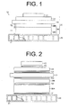
FIG. 1 is a front view of a power module according to a preferred embodiment of the present invention; -
FIG. 2 is an exploded view illustrating the manufacturing method for the power module ofFIG. 1 ; -
FIG. 3 is a front view illustrating the manufacturing method for the power module ofFIG. 1 ; -
FIG. 4 is a front view of a power module according to an alternative embodiment of the present invention; -
FIG 5A is a front view of a semiconductor device according to a prior art; -
FIG. 5B is a front view of a semiconductor device according to a preferred embodiment of the present invention; and -
FIG. 6 is a front view of a power module according to another alternative embodiment of the present invention. - The following will describe a power module as a semiconductor device according to the embodiments of the present invention with reference to
FIGS. 1 through 5 . Referring toFIG. 1 , the power module which is designated by 10 includes a double-sided substrate 30 and analuminum heat sink 20 that is formed in the shape of a plate and fixed to the bottom surface of the double-sided substrate 30. More particularly, the double-sided substrate 30 includes aceramic substrate 31, afirst aluminum layer 32 as the first metal layer of the present invention formed on the lower surface of theceramic substrate 31 and a second aluminum layer 33 (or wiring layer) as the second metal layer of the present invention formed on the upper surface of theceramic substrate 31. The ceramic substrate is made of an aluminum nitride (or AIN). - The
first aluminum layer 32 includes a plurality of subsidiary aluminum layers, namely thesubsidiary aluminum layer 32A disposed on theheat sink 20 side of thefirst aluminum layer 32 and thesubsidiary aluminum layer 32B disposed on theceramic substrate 31 side of thefirst aluminum layer 32 and laminated on thesubsidiary aluminum layer 32A. The subsidiary aluminum layer corresponds to the subsidiary metal layer of the present invention. The purity of aluminum of thesubsidiary aluminum layer 32A on theheat sink 20 side of thefirst aluminum layer 32 differs from that of thesubsidiary aluminum layer 32B on theceramic substrate 31 side of thefirst aluminum layer 32. More particularly, the purity of aluminum of thesubsidiary aluminum layer 32A (on theheat sink 20 side) is 99.99wt% or more (or 4N-Al) and the purity of aluminum of thesubsidiary aluminum layer 32B (on theceramic substrate 31 side) is 99.5wt% or more but less than 99.9wt% (or 2N-Al). The hardness (or strength) of the subsidiary aluminum layer 328 on theceramic substrate 31 side is lower than that of thesubsidiary aluminum layer 32A on theheat sink 20 side. - Additionally, the thickness T1 of the
subsidiary aluminum layer 32A on theheat sink 20 side is larger than that of thesubsidiary aluminum layer 32B on theceramic substrate 31 side. For example, thesubsidiary aluminum layer 32A on theheat sink 20 side and thesubsidiary aluminum layer 32B on theceramic substrate 31 side are formed with thicknesses of 0.5 - 3.0 mm thick and 0.2 - 0.6 mm thick, respectively. - The
first aluminum layer 32 is joined to the lower surface of theceramic substrate 31 in such a way that thesubsidiary aluminum layer 32A on theheat sink 20 side and thesubsidiary aluminum layer 32B on theceramic substrate 31 side form the lower layer and the upper layer of thefirst aluminum layer 32, respectively. Thefirst aluminum layer 32 functions as the joint layer for joining theceramic substrate 31 and theheat sink 20. - The
power module 10 further includes apower element 40 as a semiconductor element which is soldered to the upper surface of thesecond aluminum layer 33. Thus, theheat sink 20 is thermally connected to thepower element 40 through the double-sided substrate 30. Theheat sink 20 has formed therein a plurality ofparallel coolant passages 21 through which cooling water flows. During operation of thepower module 10, heat is generated by thepower element 40 and released to theheat sink 20 through the double-sided substrate 30. - The following will describe the manufacturing method for the
power module 10 with reference toFIGS. 2 and3 . Theheat sink 20, theceramic substrate 31, thesubsidiary aluminum layer 32A on theheat sink 20 side and thesubsidiary aluminum layer 32B on theceramic substrate 31 side cooperating to form thefirst aluminum layer 32 and thesecond aluminum layer 33 are joined together simultaneously by brazing. - More particularly, as shown in
FIG. 3A , thesubsidiary aluminum layer 32A is disposed on the upper surface of theheat sink 20 throughaluminum brazing flux 51 and thesubsidiary aluminum layer 32B is disposed on the upper surface of thesubsidiary aluminum layer 32A throughaluminum brazing flux 52. Next, theceramic substrate 31 is disposed on the upper surface of thesubsidiary aluminum layer 32B throughaluminum brazing flux 53 and thesecond aluminum layer 33 is disposed on the upper surface of theceramic substrate 31 throughaluminum brazing flux 54. The stack thus formed is heated in the furnace so that the aluminum brazingfluxes 51 through 54 melt. Then, the stack is placed under a room temperature to be brazed together. - Next, the
power element 40 is joined to the upper surface of thesecond aluminum layer 33 through solder 55 (FIG 2 ) by soldering. Consequently, the assembling of thepower module 10 is completed. - The following will describe the difference in the structure of semiconductor device between the prior art and the embodiment with reference to
FIGS. 5A and 5B according to the results from the structure analysis. In the structure shown inFIG. 5A of prior art, the aluminum layer 62 (or the first aluminum layer) between theceramic substrate 61 and theheat sink 60 includes the uppersubsidiary aluminum layer 62B (or 4N-Al) that is 0.6 mm thick and the lowersubsidiary aluminum layer 62A (or 2N-Al) that is 1.0 mm thick. - On the other hand, in the structure of semiconductor device shown in
FIG. 5B of the embodiment of the present invention, thefirst aluminum layer 32 between theceramic substrate 31 and theheat sink 20 includes the uppersubsidiary aluminum layer 32B (or 2N-Al) that is 0.6 mm thick and the lowersubsidiary aluminum layer 32A (or 4N-Al) that is 1.0 mm thick. - The rest of the structure of the semiconductor device according to the prior art is substantially the same as that according to the embodiment of the present invention. The following will describe the results of the structure analysis performed for the respective semiconductor devices of the prior art and the present embodiment. For the sake of convenience of explanation, the magnitude of warp in the semiconductor device according to the prior art is represented by "1.0". The magnitude of warp of the semiconductor device shown in
FIG. 5B according to the embodiment of the present invention was "0.22". That is, the magnitude of warp of the power module according to the embodiment was reduced by 78% in comparison to that according to the prior art. - As is apparent from the above comparison, the joint reliability in the structure of the semiconductor device according to the embodiment of the present invention is improved as compared with that according to the prior art. The structure of the semiconductor device according to the embodiment of the present invention offers the following advantageous effects.
- (1) The
first aluminum layer 32 includes thesubsidiary aluminum layer 32B disposed on theceramic substrate 31 side of thefirst aluminum layer 32 and thesubsidiary aluminum layer 32A disposed on theheat sink 20 side of thefirst aluminum layer 32, wherein thesubsidiary aluminum layer 32B disposed on theceramic substrate 31 side is made of aluminum whose purity is lower than that of thesubsidiary aluminum layer 32A disposed on theheat sink 20 side. In other words, the hardness (or strength) of thesubsidiary aluminum layer 32B made of aluminum (2N-Al), disposed on theceramic substrate 31 side and joined to theceramic substrate 31 by aluminum brazing is higher than that of thesubsidiary aluminum layer 32A disposed on theheat sink 20 side. Therefore, thesubsidiary aluminum layer 32B on theceramic substrate 31 side is less subject to being warped and separated from theceramic substrate 31 under heat cycle. Additionally, thesubsidiary aluminum layer 32A on theheat sink 20 side serves as a cushion member thereby to reduce the heat stress exerted on theceramic substrate 31. Thus, the joint strength between theceramic substrate 31 and thesubsidiary aluminum layer 32B on theceramic substrate 31 side of thefirst aluminum layer 32 under heat cycle is improved. - (2) The
heat sink 20 is made of an aluminum alloy. Thesubsidiary aluminum layer 32A on theheat sink 20 side of thefirst aluminum layer 32 and theheat sink 20 are made of the same kind of material, so that the joint strength between thesubsidiary aluminum layer 32A on theheat sink 20 side and theheat sink 20 is improved. - (3) The double-
sided substrate 30 and theheat sink 20 can be joined simultaneously by brazing. - The present invention is not limited to the above embodiment, but it may be modified into various alternative embodiments, as exemplified below.
- As shown in
FIG. 4 , ahole 32C (or a recess) may be formed through thesubsidiary aluminum layer 32A on theheat sink 20 side of thefirst aluminum layer 32. The provision ofsuch hole 32C in thesubsidiary aluminum layer 32A helps to reduce the heat stress exerted on theceramic substrate 31, thereby improving the joint strength of the semiconductor device. A hole (or a recess) may be formed through thesubsidiary aluminum layer 32B on theceramic substrate 31 side of thefirst aluminum layer 32. - The
first aluminum layer 32 may include three subsidiary aluminum layers or more, as shown inFIG. 6 . The subsidiary aluminum layer corresponds to the subsidiary metal layer of the present invention. In this case, the closer to theceramic substrate 31 any subsidiary aluminum layer is located, the lower purity of aluminum and the smaller thickness the subsidiary aluminum layer needs to have. For example, thefirst aluminum layer 32 may include three subsidiary aluminum layers, namely a subsidiary aluminum layer 71A made of 2N-Al, asubsidiary aluminum layer 71 B made of 3N-Al and a subsidiary aluminum layer 71C made of 4N-Al that are laminated in this order as seen from the lower surface of theceramic substrate 31. The thickness T3, T4, T5 of the respective aluminum layers made of 2N-Al, 3N-Al, 4N-Al are increased in this order. This structure improves the joint strength between theceramic substrate 31 and thefirst aluminum layer 32 and the heat stress is reduced by the subsidiary aluminum layer 71C that is made of 4N-Al. - Alcohol and the like may be used as the coolant flowing through the
coolant passages 21 of theheat sink 20. Theheat sink 20 of thepower module 10 may be of an air-cooling type releasing heat to the atmosphere. - The plurality of metal layers forming the first metal layer and having different purities may be made of copper instead of aluminum.
- The
heat sink 20 may be made of copper. - A double-sided substrate includes a ceramic substrate, a first metal layer formed on one surface of the ceramic substrate and having a plurality of subsidiary metal layers which are laminated on the surface of the ceramic substrate and whose purities differ from each other and a second metal layer formed on the other surface of the ceramic substrate, wherein the closer to the ceramic substrate any subsidiary metal layer is located, the lower purity the subsidiary metal layer has. Additionally, a semiconductor includes the above double-sided substrate, a power element and a heat sink.
Claims (9)
- A double-sided substrate (30) comprising:a ceramic substrate (31);a first metal layer (32) formed on one surface of the ceramic substrate (31) and having a plurality of subsidiary metal layers (32A, 32B, 71A, 71B, 71C) which are laminated on the surface of the ceramic substrate (31) and whose purities differ from each other; anda second metal layer (33) formed on the other surface of the ceramic substrate (31), characterized in that the closer to the ceramic substrate (31) any subsidiary metal layer (32B, 71A) is located, the lower purity the subsidiary metal layer (32B, 71A) has.
- The double-sided substrate (30) according to claim 1, characterized in that the higher purity any subsidiary metal layer (32A, 71C) has, the larger thickness the subsidiary metal layer (32A, 71C) has.
- The double-sided substrate (30) according to any one of claims 1 and 2, characterized in that the subsidiary metal layer (32B, 71A) closer to the ceramic substrate (31) is formed with thickness of 0.2 - 0.6mm and the subsidiary metal layer (32A, 71C) far from the ceramic substrate (31) is formed with thickness of 0.5 - 3.0mm.
- The double-sided substrate (30) according to any one of claims 1 through 3, characterized in that the subsidiary metal layer (32A) has a hole (32C).
- The double-sided substrate (30) according to any one of claims 1 through 4, characterized in that the subsidiary metal layers (32A, 328, 71A, 71 B, 71C) are made of aluminum, wherein the purity of aluminum of the subsidiary metal layer (32B, 71A) having the lowest purity among the subsidiary metal layers (32A, 32B, 71A, 71 B, 71 C) is 99.5wt% or more, but less than 99.9wt%, wherein the purity of aluminum of the subsidiary metal layer (32A, 71 C) having the highest purity among the subsidiary metal layers (32A, 32B, 71A, 71 B, 71C) is 99.99wt% or more.
- The double-sided substrate (30) according to any one of claims 1 through 4, characterized in that the first and the second metal layers (32, 33) are made of copper.
- A semiconductor device (10) characterized in that the semiconductor device (10) comprising:the double-sided substrate (30) according to any one of claims 1 through 6;a power element (40): anda heat sink (60)
- The semiconductor device (10) according to claim 7, characterized in that the heat sink (60) is made of the same kind of material as the first and the second metal layers.
- A method of manufacturing a semiconductor device including a ceramic substrate (31), a plurality of subsidiary metal layers (32A, 32B, 71A, 71B, 71C) forming a first metal layer (32), a second metal layer (33), a heat sink (60) and a power element (40), wherein purities of the plurality of subsidiary metal layers (32A, 32B, 71A, 71B, 71C) differ from each other, wherein the closer to the ceramic substrate (31) any subsidiary metal layer (32B, 71A) is located, the lower purity the subsidiary metal layer (32B, 71A) has, characterized by the steps of:joining the ceramic substrate (31), the plurality of subsidiary metal layers (32A, 328, 71A, 71B, 71C) forming the first metal layer (32), the second metal layer (33) and the heat sink (60) simultaneously by brazing in a first manufacturing process; andjoining the power element (40) to the second metal layer (33) by soldering in a second manufacturing process.
Applications Claiming Priority (1)
| Application Number | Priority Date | Filing Date | Title |
|---|---|---|---|
| JP2011005019A JP5392272B2 (en) | 2011-01-13 | 2011-01-13 | Double-sided substrate, semiconductor device, and method for manufacturing semiconductor device |
Publications (2)
| Publication Number | Publication Date |
|---|---|
| EP2477218A2 true EP2477218A2 (en) | 2012-07-18 |
| EP2477218A3 EP2477218A3 (en) | 2016-06-01 |
Family
ID=45443042
Family Applications (1)
| Application Number | Title | Priority Date | Filing Date |
|---|---|---|---|
| EP12150715.6A Withdrawn EP2477218A3 (en) | 2011-01-13 | 2012-01-11 | Double-sided substrate, semiconductor device and method for the same |
Country Status (3)
| Country | Link |
|---|---|
| US (1) | US8735729B2 (en) |
| EP (1) | EP2477218A3 (en) |
| JP (1) | JP5392272B2 (en) |
Families Citing this family (10)
| Publication number | Priority date | Publication date | Assignee | Title |
|---|---|---|---|---|
| KR101610973B1 (en) * | 2008-03-17 | 2016-04-08 | 미쓰비시 마테리알 가부시키가이샤 | Substrate for power module with heat sink and method for producing the same, power module with heat sink, and substrate for power module |
| JP5918008B2 (en) * | 2012-05-08 | 2016-05-18 | 昭和電工株式会社 | Manufacturing method of cooler |
| JP6341822B2 (en) * | 2014-09-26 | 2018-06-13 | 三菱電機株式会社 | Semiconductor device |
| DE112015006049B4 (en) * | 2015-01-26 | 2024-10-10 | Mitsubishi Electric Corporation | Semiconductor component and method for producing a semiconductor component |
| JP6681660B2 (en) * | 2015-03-09 | 2020-04-15 | 三菱マテリアル株式会社 | Substrate for power module with heat sink and power module |
| JP6137267B2 (en) | 2015-10-08 | 2017-05-31 | 三菱マテリアル株式会社 | Power module substrate with heat sink and power module |
| JP2017224748A (en) * | 2016-06-16 | 2017-12-21 | 株式会社Uacj | Heat sink with circuit board and manufacturing method thereof |
| EP3263537B1 (en) * | 2016-06-27 | 2021-09-22 | Infineon Technologies AG | Method for producing a metal-ceramic substrate |
| TWI667221B (en) * | 2018-11-14 | 2019-08-01 | 國家中山科學研究院 | Method for reducing interface stress accumulation on double-sided copper plating layer and aluminum nitride substrate |
| CN113145963B (en) * | 2021-06-08 | 2023-05-02 | 广西易德科技有限责任公司 | Water nozzle welding method for water chamber of water-cooled radiator |
Citations (1)
| Publication number | Priority date | Publication date | Assignee | Title |
|---|---|---|---|---|
| JP2009065144A (en) | 2007-08-16 | 2009-03-26 | Mitsubishi Materials Corp | Power module substrate, manufacturing method thereof, and power module |
Family Cites Families (11)
| Publication number | Priority date | Publication date | Assignee | Title |
|---|---|---|---|---|
| JP4077181B2 (en) * | 2001-09-27 | 2008-04-16 | 本田技研工業株式会社 | Metal or ceramic bonding material and metal or ceramic bonding method |
| JP4206915B2 (en) * | 2002-12-27 | 2009-01-14 | 三菱マテリアル株式会社 | Power module substrate |
| EP2112249A1 (en) * | 2005-05-26 | 2009-10-28 | Nanocomp Technologies, Inc. | Systems and methods for thermal management of electronic components |
| JP4037425B2 (en) * | 2005-07-04 | 2008-01-23 | 電気化学工業株式会社 | Ceramic circuit board and power control component using the same. |
| JP4617209B2 (en) * | 2005-07-07 | 2011-01-19 | 株式会社豊田自動織機 | Heat dissipation device |
| EP2003691B1 (en) * | 2006-03-13 | 2019-01-09 | Showa Denko K.K. | Base for power module |
| JP4916737B2 (en) * | 2006-03-14 | 2012-04-18 | 三菱マテリアル株式会社 | Cooler |
| JP4786407B2 (en) * | 2006-05-18 | 2011-10-05 | 三菱マテリアル株式会社 | Power module |
| KR101610973B1 (en) * | 2008-03-17 | 2016-04-08 | 미쓰비시 마테리알 가부시키가이샤 | Substrate for power module with heat sink and method for producing the same, power module with heat sink, and substrate for power module |
| JP2010171279A (en) * | 2009-01-23 | 2010-08-05 | Toyota Motor Corp | Heat radiator |
| JP6189015B2 (en) * | 2012-04-19 | 2017-08-30 | 昭和電工株式会社 | Radiator and method of manufacturing radiator |
-
2011
- 2011-01-13 JP JP2011005019A patent/JP5392272B2/en not_active Expired - Fee Related
-
2012
- 2012-01-10 US US13/346,978 patent/US8735729B2/en not_active Expired - Fee Related
- 2012-01-11 EP EP12150715.6A patent/EP2477218A3/en not_active Withdrawn
Patent Citations (1)
| Publication number | Priority date | Publication date | Assignee | Title |
|---|---|---|---|---|
| JP2009065144A (en) | 2007-08-16 | 2009-03-26 | Mitsubishi Materials Corp | Power module substrate, manufacturing method thereof, and power module |
Also Published As
| Publication number | Publication date |
|---|---|
| US8735729B2 (en) | 2014-05-27 |
| JP5392272B2 (en) | 2014-01-22 |
| US20120182692A1 (en) | 2012-07-19 |
| JP2012146864A (en) | 2012-08-02 |
| EP2477218A3 (en) | 2016-06-01 |
Similar Documents
| Publication | Publication Date | Title |
|---|---|---|
| US8735729B2 (en) | Double-sided substrate, semiconductor device and method for the same | |
| US10068829B2 (en) | Power-module substrate unit and power module | |
| KR101610973B1 (en) | Substrate for power module with heat sink and method for producing the same, power module with heat sink, and substrate for power module | |
| EP3166140B1 (en) | Substrate unit for power modules, and power module | |
| KR101188150B1 (en) | Cooling system | |
| TWI727146B (en) | Substrate for power module with heat sink attached | |
| KR102300972B1 (en) | Substrate unit for power modules, and power module | |
| JP6435945B2 (en) | Power module board with heat sink | |
| US10453772B2 (en) | Heat-sink-attached power-module substrate and power module | |
| JP5759902B2 (en) | Laminate and method for producing the same | |
| TWI750332B (en) | Substrate for power module with heat sink attached | |
| US20170047268A1 (en) | Power-module substrate, heat-sink-attached power-module substrate, and heat-sink-attached power module | |
| JP6417834B2 (en) | Power module substrate with cooler and method for manufacturing power module substrate with cooler | |
| JP6435711B2 (en) | Power module substrate with heat sink and power module | |
| JP5914968B2 (en) | Power module substrate with heat sink and manufacturing method thereof | |
| JP5131205B2 (en) | Power module substrate manufacturing method | |
| JP5887939B2 (en) | Manufacturing method and manufacturing apparatus for power module substrate with heat sink | |
| JP5887907B2 (en) | Power module substrate manufacturing method and manufacturing apparatus | |
| HK1151627A (en) | Substrate for power module with heat sink and method for producing the same, power module with heat sink, and substrate for power module |
Legal Events
| Date | Code | Title | Description |
|---|---|---|---|
| PUAI | Public reference made under article 153(3) epc to a published international application that has entered the european phase |
Free format text: ORIGINAL CODE: 0009012 |
|
| 17P | Request for examination filed |
Effective date: 20120111 |
|
| AK | Designated contracting states |
Kind code of ref document: A2 Designated state(s): AL AT BE BG CH CY CZ DE DK EE ES FI FR GB GR HR HU IE IS IT LI LT LU LV MC MK MT NL NO PL PT RO RS SE SI SK SM TR |
|
| AX | Request for extension of the european patent |
Extension state: BA ME |
|
| PUAL | Search report despatched |
Free format text: ORIGINAL CODE: 0009013 |
|
| AK | Designated contracting states |
Kind code of ref document: A3 Designated state(s): AL AT BE BG CH CY CZ DE DK EE ES FI FR GB GR HR HU IE IS IT LI LT LU LV MC MK MT NL NO PL PT RO RS SE SI SK SM TR |
|
| AX | Request for extension of the european patent |
Extension state: BA ME |
|
| RIC1 | Information provided on ipc code assigned before grant |
Ipc: H01L 23/373 20060101AFI20160426BHEP Ipc: C04B 37/02 20060101ALI20160426BHEP |
|
| STAA | Information on the status of an ep patent application or granted ep patent |
Free format text: STATUS: THE APPLICATION IS DEEMED TO BE WITHDRAWN |
|
| 18D | Application deemed to be withdrawn |
Effective date: 20161202 |