EP2477075A1 - An image forming device - Google Patents
An image forming device Download PDFInfo
- Publication number
- EP2477075A1 EP2477075A1 EP09849201A EP09849201A EP2477075A1 EP 2477075 A1 EP2477075 A1 EP 2477075A1 EP 09849201 A EP09849201 A EP 09849201A EP 09849201 A EP09849201 A EP 09849201A EP 2477075 A1 EP2477075 A1 EP 2477075A1
- Authority
- EP
- European Patent Office
- Prior art keywords
- charging
- photosensitive member
- photoconductor drum
- light
- image
- Prior art date
- Legal status (The legal status is an assumption and is not a legal conclusion. Google has not performed a legal analysis and makes no representation as to the accuracy of the status listed.)
- Withdrawn
Links
Images


Classifications
-
- G—PHYSICS
- G03—PHOTOGRAPHY; CINEMATOGRAPHY; ANALOGOUS TECHNIQUES USING WAVES OTHER THAN OPTICAL WAVES; ELECTROGRAPHY; HOLOGRAPHY
- G03G—ELECTROGRAPHY; ELECTROPHOTOGRAPHY; MAGNETOGRAPHY
- G03G15/00—Apparatus for electrographic processes using a charge pattern
- G03G15/02—Apparatus for electrographic processes using a charge pattern for laying down a uniform charge, e.g. for sensitising; Corona discharge devices
- G03G15/0266—Arrangements for controlling the amount of charge
-
- G—PHYSICS
- G03—PHOTOGRAPHY; CINEMATOGRAPHY; ANALOGOUS TECHNIQUES USING WAVES OTHER THAN OPTICAL WAVES; ELECTROGRAPHY; HOLOGRAPHY
- G03G—ELECTROGRAPHY; ELECTROPHOTOGRAPHY; MAGNETOGRAPHY
- G03G15/00—Apparatus for electrographic processes using a charge pattern
- G03G15/02—Apparatus for electrographic processes using a charge pattern for laying down a uniform charge, e.g. for sensitising; Corona discharge devices
- G03G15/0208—Apparatus for electrographic processes using a charge pattern for laying down a uniform charge, e.g. for sensitising; Corona discharge devices by contact, friction or induction, e.g. liquid charging apparatus
- G03G15/0216—Apparatus for electrographic processes using a charge pattern for laying down a uniform charge, e.g. for sensitising; Corona discharge devices by contact, friction or induction, e.g. liquid charging apparatus by bringing a charging member into contact with the member to be charged, e.g. roller, brush chargers
-
- G—PHYSICS
- G03—PHOTOGRAPHY; CINEMATOGRAPHY; ANALOGOUS TECHNIQUES USING WAVES OTHER THAN OPTICAL WAVES; ELECTROGRAPHY; HOLOGRAPHY
- G03G—ELECTROGRAPHY; ELECTROPHOTOGRAPHY; MAGNETOGRAPHY
- G03G15/00—Apparatus for electrographic processes using a charge pattern
- G03G15/50—Machine control of apparatus for electrographic processes using a charge pattern, e.g. regulating differents parts of the machine, multimode copiers, microprocessor control
- G03G15/5004—Power supply control, e.g. power-saving mode, automatic power turn-off
-
- G—PHYSICS
- G03—PHOTOGRAPHY; CINEMATOGRAPHY; ANALOGOUS TECHNIQUES USING WAVES OTHER THAN OPTICAL WAVES; ELECTROGRAPHY; HOLOGRAPHY
- G03G—ELECTROGRAPHY; ELECTROPHOTOGRAPHY; MAGNETOGRAPHY
- G03G21/00—Arrangements not provided for by groups G03G13/00 - G03G19/00, e.g. cleaning, elimination of residual charge
- G03G21/06—Eliminating residual charges from a reusable imaging member
- G03G21/08—Eliminating residual charges from a reusable imaging member using optical radiation
-
- G—PHYSICS
- G03—PHOTOGRAPHY; CINEMATOGRAPHY; ANALOGOUS TECHNIQUES USING WAVES OTHER THAN OPTICAL WAVES; ELECTROGRAPHY; HOLOGRAPHY
- G03G—ELECTROGRAPHY; ELECTROPHOTOGRAPHY; MAGNETOGRAPHY
- G03G2215/00—Apparatus for electrophotographic processes
- G03G2215/00025—Machine control, e.g. regulating different parts of the machine
- G03G2215/00071—Machine control, e.g. regulating different parts of the machine by measuring the photoconductor or its environmental characteristics
- G03G2215/00075—Machine control, e.g. regulating different parts of the machine by measuring the photoconductor or its environmental characteristics the characteristic being its speed
Definitions
- the present invention relates to an electrophotographic image forming apparatus such as a copying machine, a printer, or a FAX.
- Recent electrophotographic image forming apparatuses use a method for, in order to charge a photosensitive member, bringing a roller or blade charging member into contact with the photosensitive member to charge the photosensitive member.
- Two methods are well known to charge a photosensitive member by using a contact charging method.
- the first method is an "AC charging method” in which a superimposed voltage of direct-current voltage and alternating-current voltage is applied to a charging member to charge a photosensitive member
- the second method is a "DC charging method” in which only a direct-current voltage is applied to a charging member to charge a photosensitive member. Due to the application of an alternating-current voltage, the "AC charging method” allows a more uniform charging of the surface of a photosensitive member than the "DC charging method".
- the amount of discharge to the photosensitive member is larger than that in the "DC charging method", and therefore the surface of the photosensitive member is more easily scraped.
- the life of the photosensitive member will be shorter than that when the photosensitive member is charged using the "DC charging method”.
- the "AC charging method” requires an AC power source.
- the "AC charging method” has a greater initial cost and a higher running cost than that required for the "DC charging method”.
- the "DC charging method” is more advantageous than the "AC charging method” in terms of running cost and initial cost.
- the uniformity of surface potential of a photosensitive member is lower in the “DC charging method” than the charging uniformity in the "AC charging method".
- a problem of stripe-shaped charging non-uniformity (charging lateral stripe) in the longitudinal direction (direction perpendicular to the circumferential direction) of an electrophotographic photosensitive member which is caused by the non-uniform surface potential of the photosensitive member.
- this is caused by the occurrence of separating discharge in a charging gap (fine gap) located downstream in the rotation direction of a photosensitive drum, between the photosensitive member that is charged in a charging gap located upstream in the rotation direction of the photosensitive drum and a charging roller.
- a configuration for suppressing formation of a "charging lateral stripe” that occurs when a photosensitive member is charged using the "DC charging method” is disclosed in PTL 1.
- a charging gap located upstream in the rotation direction of the photosensitive member is irradiated with light (pre-nip exposure). Therefore, the charge of the photosensitive member is canceled in the charging gap located upstream, and the photosensitive member is charged in a charging gap located downstream in the rotation direction of the photosensitive member. In turn, this suppresses the occurrence of a charging lateral stripe caused by separating discharge.
- an apparatus having a photosensitive member that moves at each process speed has had a problem in that a charging lateral stripe occurs if a charging gap located upstream in the rotation direction of the photosensitive member is irradiated with constant light regardless of the process speed (rotational speed of the photosensitive member).
- a charging lateral stripe occurs if the charging gap located upstream is exposed to light at an amount that is equal to the amount of light exposed to a charging gap located upstream when an image is to be formed on thick paper.
- this is caused by the occurrence of separating discharge in a charging gap located downstream because if the process speed is low, the photosensitive member is sufficiently charged in the charging gap located upstream even when the charging gap located upstream is subjected to erasure with light.
- the present invention provides an image forming apparatus including a rotatable photosensitive member, a charging member that is in contact with the photosensitive member to charge the photosensitive member, a power source that applies a direct-current voltage to the charging member, and irradiation means for irradiating a charging gap located upstream in a rotation direction of the photosensitive member with light among charging gaps at which the charging member charges the photosensitive member, wherein the image forming apparatus further includes control means for controlling the irradiation means to irradiate the charging gap located upstream with light of a first light amount when the photosensitive member rotates at a first speed, and to irradiate the charging gap located upstream with light of a second light amount that is larger than the first light amount when the photosensitive member rotates at a second speed that is lower than the first speed.
- the occurrence of a charging lateral stripe can be suppressed even when the rotational speed of the photosensitive member is changed.
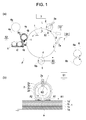
- Fig. 1 includes schematic diagrams describing the overall configuration of an image forming apparatus.
- an image forming apparatus is an electrophotographic image forming apparatus that uses a roller charging device to charge a photosensitive drum. More specifically, the image forming apparatus is a laser beam printer capable of forming an image on paper up to A3 size, which adopts a contact charging method in which a charging roller is brought into contact with the photosensitive drum and a reversal developing method in which a region where a toner image is to be formed is exposed to light.
- a photoconductor drum 1 that is a drum-shaped photosensitive member is a negative chargeable organic photoconductor (OPC) with an outer diameter of 30 mm, and is caused to rotate by a driving force from a motor (not illustrated) serving as a driving device.
- OPC organic photoconductor
- the photoconductor drum 1 is driven to rotate in the arrow direction (counterclockwise) at a peripheral speed (hereinafter referred to as a process speed) of 210 mm/s when an image is to be formed on plain paper, and at a peripheral speed of 105 mm/s when an image is to be formed on thick paper.
- a process speed peripheral speed
- the photoconductor drum 1 is configured by coating a surface of an aluminum cylinder (conductive drum base) 1a with three layers of an undercoating layer 1b for improving adhesiveness of upper layers while reducing optical interference, a photocharge generating layer 1c, and a charge transport layer 1d in order from the bottom.
- a charging roller 2 serving as a charging member, which is in contact with the photoconductor drum 1, a developing device 4, a transfer roller 5, and a cleaning device 7 are arranged around the photoconductor drum 1 along the rotation direction (counterclockwise) thereof.
- an exposure device 3 serving as electrostatic image forming means is provided above the photoconductor drum 1 between the charging roller 2 and the developing device 4.
- a fixing device 6 is provided downstream in a transfer material conveying direction of a transfer portion d formed by the photoconductor drum 1 and the transfer roller 5.
- the charging roller 2 that charges the photoconductor drum 1 is held in a rotatable manner at both ends of a core metal 2a by bearing members (not illustrated).
- a pressure spring 2e urges the charging roller 2 toward the center of the photoconductor drum 1 so that the charging roller 2 is pressed against the surface of the photoconductor drum 1 with a predetermined pressing force.
- the charging roller 2 rotates in accordance with the rotational driving of the photoconductor drum 1.
- the photoconductor drum 1 and the charging roller 2 are brought into contact with each other to form a contact portion.
- the gap between the photoconductor drum 1 and the charging roller 2 increases in the rotation direction of the photosensitive member from the contact portion.
- the pressed portion (contact portion) between the photoconductor drum 1 and the charging roller 2 is referred to as a charging nip portion.
- a fine gap located upstream the pressed portion in the rotation direction of the photoconductor drum 1 is referred to as an upstream-side charging gap A1.
- a fine gap located downstream the pressed portion in the rotation direction of the photoconductor drum 1 is referred to as a downstream-side charging gap A2.
- the photoconductor drum 1 is charged in the upstream-side charging gap A1 and the downstream-side charging gap A2 with respect to the pressed portion.
- the charging of the photoconductor drum 1 is performed by discharging from the charging roller 2 to the photoconductor drum 1.
- a voltage greater than or equal to a threshold voltage at which discharge starts is applied to the charging roller 2.
- a voltage greater than or equal to about -600 V is applied to the charging roller 2
- the surface potential of the photosensitive member starts to increase.
- the surface potential of the photoconductor drum 1 increases after the application of about -600 V while keeping substantially the linear relationship with applied voltages.
- if -900 V is applied to the charging roller 2 the surface of the photoconductor drum 1 reaches -300 V. Further, if -1100 V is applied to the charging roller 2, the surface of the photoconductor drum 1 reaches -500 V.
- This threshold voltage (-600 V) is hereinafter referred to as a discharge start voltage (charging start voltage) Vth (V). That is, in an electrophotographic image forming process, it is necessary to apply Vd+Vth (V) to the charging roller 2 to charge the potential on the surface of the photoconductor drum 1 to Vd (V) (dark potential). In other words, a voltage of Vd+Vth (V) is applied to the core metal 2a of the charging roller 2 by a power source S1, thus allowing the potential on the surface of the photoconductor drum 1 to reach Vd (V). In the image forming apparatus of the exemplary embodiment, in order to form an image, the dark potential Vd is set to -500 V when the photoconductor drum 1 is charged.
- a direct-current voltage (hereinafter referred to as a DC bias) of -1100 V is applied to the charging roller 2 from the direct-current power source S1.
- a DC bias a direct-current voltage
- the width of the charging gap in the photosensitive drum direction at which the charging roller charges the photoconductor drum 1 by discharging changes depending on the voltage applied to the charging roller. That is, while a charging gap refers to a portion where the photoconductor drum is charged by the occurrence of discharging, it is known that a fine gap in which a discharge occurs when a voltage is applied changes in accordance with Paschen's law. Note that a portion where the photoconductor drum 1 is charged when a bias is applied to the charging roller 2 in the state where the rotation of the photoconductor drum 1 is stopped corresponds to a charging gap.
- the longitudinal length of the charging roller 2 is 320 mm.
- the charging roller 2 has a three-layer configuration in which a lower layer 2b, an intermediate layer 2c, and a surface layer 2d are stacked in this order around the core metal (supporting member) 2a.
- the lower layer 2b is a foamed sponge layer for reducing charging sound.
- the surface layer 2d acts as a protective layer for preventing leakage of current even if the photoconductor drum 1 has a defect thereon such as a pinhole.
- the core metal 2a is a stainless round bar with a diameter of 6 mm.
- the lower layer 2b is composed of foamed EPDM with carbon dispersed therein with a thickness of 3.0 mm. Note that foamed EPDM having a specific gravity of 0.5 g/cm 3 and a volume resistance of 102 to 109 ⁇ cm is used.
- the intermediate layer 2c is composed of NBR-based rubber with carbon dispersed (a volume resistance of 102 to 105 ⁇ cm) with a thickness of 700 ⁇ m.
- the surface layer 2d is formed of Toresin resin, which is a fluorinated compound, with a thickness of 10 ⁇ m. Note that Toresin resin with tin oxide and carbon dispersed therein and having a volume resistance of 107 to 1010 ⁇ cm is used. Further, the surface roughness of the charging roller 2 (10-point average surface roughness Ra in JIS) is 1.5 ⁇ m.
- the exposure device 3 serving as electrostatic image forming means for forming an electrostatic image on the charged photoconductor drum 1 will be described.
- the exposure device 3 is a laser beam scanner using a semiconductor laser.
- the exposure device 3 outputs a laser beam that is modulated in accordance with an image signal input from a host processor such as an image reading device (not illustrated).
- the laser beam is scanned at an exposure position b on the surface of the charged photoconductor drum 1, and an electrostatic image corresponding to the input image signal is formed on the photoconductor drum 1 (on the photosensitive member).
- the developing device 4 develops the electrostatic image formed on the photoconductor drum 1.
- a two-component developer is used, and an electrostatic image is developed using a magnetic brush.
- the electrostatic image is developed by attaching toner to an exposed portion (bright portion) of the surface of the photoconductor drum 1.
- the configuration of the developing device 4 will be described in detail hereinafter.
- the developing device 4 includes a developing container 4a, and a rotatable non-magnetic developing sleeve 4b disposed at an opening of the developing container, which includes a fixed magnet roller 4c.
- a regulating blade 4d regulates a developer 4e containing toner and carrier (magnetic particles), which is accommodated in the developing container 4a, to obtain a certain thickness.
- the internal magnet causes the magnetic brush to be erected by the carrier, and the toner is conveyed to a developing portion c where the developing sleeve 4b faces the photoconductor drum 1.
- the developer 4e in the developing container 4a is a mixture of toner and magnetic carrier.
- the developer 4e is conveyed toward the developing sleeve 4b while being stirred uniformly by the rotation of two developer stirring members 4f (stirring screws).
- the magnetic carrier has a resistance of about 1013 ⁇ cm and a particle diameter of about 40 ⁇ m.
- the toner is rubbed with the magnetic carrier and is therefore frictionally charged to the negative polarity.
- a density sensor (not illustrated) detects the toner density in the developing container 4a.
- the toner is replenished into the developing container 4a from a toner hopper 4g based on detection information detected by the density sensor so that the toner density in the developing container can be made uniform.
- the developing sleeve 4b is provided to face the photoconductor drum 1 in close proximity thereto while keeping the closest distance at the developing portion c from the photoconductor drum 1 at 300 ⁇ m.
- the developing sleeve 4b is driven to rotate in the direction opposite to the rotation direction (counterclockwise) of the photoconductor drum 1 at the developing portion c.
- a predetermined developing bias is applied to the developing sleeve 4b from a power source S2.
- a developing bias in which a direct-current voltage (Vdc) and an alternating-current voltage (Vac) are superimposed is applied to the developing sleeve 4b.
- the frequency of the alternating-current voltage is 8 kHz
- the direct-current voltage is -320 V
- the peak-to-peak voltage Vpp of the alternating-current voltage is 1800 V.
- a toner image formed on the photoconductor drum 1 through the developing step is transferred onto a sheet in a transfer step.
- the transfer roller 5 abuts against the photoconductor drum 1 with a predetermined pressing force to form the transfer portion d.
- a transfer bias positive transfer bias having a polarity that is opposite to the normal charged polarity of the toner, i.e., negative polarity; in the embodiment, +500 V
- a transfer bias positive transfer bias having a polarity that is opposite to the normal charged polarity of the toner, i.e., negative polarity; in the embodiment, +500 V
- the cleaning device 7 cleans toner that is not transferred onto the sheet from the photoconductor drum 1.
- the cleaning device 7 includes a cleaning blade 7a. Untransferred residual toner that is still attached to the photosensitive drum 1 is contacted with the cleaning blade 7a and is therefore removed.
- reference numeral e denotes a photosensitive drum surface abutting portion of the cleaning blade 7a.
- the fixing device 6 that fixes a toner image onto a sheet includes a rotatable fixing roller 6a and a pressure roller 6b.
- the fixing device 6 fixes the toner image transferred onto the sheet by heating and pressing the toner image while conveying the sheet that is being held therebetween.
- a control circuit controls the rotational speeds of the fixing roller 6a and the pressure roller 6bin accordance with the material, thickness, basis weight, etc. of the sheet.
- the fixing roller 6a and the pressure roller 6b rotate so that the process speed can reach 105 mm/s when an image is to be fixed onto thick paper (having basis weight of 101 to 200 g/m 2 ). Further, the fixing roller 6a and the pressure roller 6b rotate so that the process speed can reach 210 mm/s when an image is to be fixed onto plain paper (having basis weight 50 to 100 g/m 2 ).
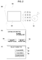
- Fig. 4 includes diagrams describing an operation panel.
- Part (a) of Fig. 4 is a diagram describing the outer appearance of an operation panel 100.
- the operation panel 100 includes a start button 101 for allowing the image forming apparatus to execute image formation based on set information.
- the operation panel 100 further includes a touch-panel display 102.
- a screen as illustrated in part (b) of Fig. 2 is displayed on the display 102.
- a user can select a button displayed on the display 102 to perform various settings for image formation.
- the setting of the type of a sheet on which an image is to be formed and a quality priority mode will be described in detail.
- reference numeral 103 denotes a button for setting the type of a sheet on which an image is to be formed.
- a screen in part (c) of Fig. 2 is displayed on the display 102.
- part (c) of Fig. 2 a list of sheets available for image formation is displayed.
- a user can select one of plain paper 104, thick paper 105, coated paper, and the like in accordance with the type of the sheet to be used for image formation. As described above, when the plain paper 104 is selected, the process speed is set to 210 mm/s. Further, when the thick paper 105 is selected, the process speed is set to 105 mm/s.
- Coated paper is a glossy sheet whose surface smoothness is improved by coating the surface of the sheet with a transparent resin.
- the process speed is also set to 105 mm/s.
- the type of the sheet may not necessarily be set by a user but may be determined using a sensor or the like.
- reference numeral 104 denotes a button for specifying a high-quality mode. With the use of this button, when an image is to be formed on plain paper, the process speed is also changed to 105 mm/s. The reduction of the process speed allows an electrostatic image having a higher resolution than that at a high process speed to be formed on the photoconductor drum 1.
- the image forming apparatus forms an image in accordance with the set conditions.
- a printing instruction may also be input from an external terminal such as a PC.
- FIG. 3 is a diagram describing a pre-nip exposure device that exposes a charging gap to light. Applying a direct-current voltage from the power source S1 to the charging roller 2 charges the photoconductor drum 1. Further, a power source S4 supplies power to a pre-nip exposure device 8 in accordance with the control of a control circuit 200. The pre-nip exposure device 8 radiates light to an upstream-side charging gap in the rotation direction of the photoconductor drum 1.
- the pre-nip exposure device 8 exposes the upstream-side charging gap in the rotation direction of the photoconductor drum 1 to light from a nip portion between the photoconductor drum 1 and the charging roller 2, and an image forming region is erased in the longitudinal direction of the photoconductor drum 1.
- an LED Light Emitting Diode
- a peak wavelength of 660 ( ⁇ 10) nm at a room temperature (20°C) is used as the pre-nip exposure device 8. It is known that the wavelength of emitted light changes depending on the temperature of the material and the applied current.
- an LED having a forward drop voltage of 1.4 V, a maximum rated output of 3 mW, a maximum operating current of 95 mA, a maximum output of 2.1 mW, and a luminous efficiency of 39 lm/W is used.
- a multiple number of such LEDs are arranged side-by-side, and an LED driver applies a PWM (Pulse Width Modulated) voltage to the LEDs to allow control of the light amount of the pre-nip exposure device.
- PWM Pulse Width Modulated
- the upstream-side charging gap A1 is a region that is located 1 mm away upstream in the rotation direction of the photoconductor drum 1 from the nip portion between the photoconductor drum 1 and the charging roller 2.
- the downstream-side charging gap A2 is a region that is located 1 mm away downstream in the rotation direction of the photoconductor drum 1 from the nip portion between the photoconductor drum 1 and the charging roller 2.
- the control circuit 200 serving as control means includes a CPU, a RAM, etc., and controls individual units of the image forming apparatus in accordance with an image forming signal input from the operation panel 100 serving as an operation unit or an external terminal such as a PC. For example, the control circuit 200 obtains information or the like about a sheet specified using the operation panel 100, and determines the process speed accordingly. Further, the control circuit 200 controls the image forming condition of each image forming unit in accordance with the process speed. Specifically, by way of example, the control circuit 200 is capable of controlling power to be supplied to the pre-nip exposure device 8 from the power source S4.
- the pre-nip exposure device 8 can output light of 0 to 15 1x ⁇ s per unit time.
- the light amount is measured using an illuminometer that conforms to general class AA of JIS C 1609-1 (revised 2006).
- the illuminometer measures the light amount in a visible light region (420 to 700 nm).
- a photodiode may be used to detect a change in the light amount in a region other than the visible light region.
- a photodiode detects light transmitted through an optical filter that cuts the wavelength to which the photosensitive member is less sensitive.
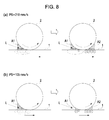
- Fig. 8 includes schematic diagrams describing a separating discharge phenomenon that occurs in the photoconductor drum 1 when the upstream-side charging gap in the rotation direction of the photoconductor drum 1 is exposed to light with a constant light amount in order to suppress formation of a charging lateral stripe.
- Part (a) of Fig. 8 is a schematic diagram of the upstream-side charging gap exposed to light when the process speed is 210 mm/s.
- part (b) of Fig. 8 is a schematic diagram of the upstream-side charging gap exposed to light with a light amount (7 1x ⁇ s), which is the same as that when the process speed is 210 mm/s, when the process speed is 105 mm/s.
- the charging roller 2 rotates forward relative to the photoconductor drum 1 that is rotating, and the photoconductor drum 1 is charged.
- the upstream-side charging gap A1 when the potential difference between the photoconductor drum 1 and the charging roller 2 exceeds a discharge start threshold (based on Paschen's law), discharge is performed, and the photoconductor drum 1 is charged to the charging potential (Vd).
- Vd charging potential
- the resistance of a portion of the charging roller 2 is high or a portion of the photoconductor drum 1 is thick, uniform charging may not be completed in the upstream-side charging gap A1. In this case, minute discharge occurs in the downstream-side charging gap A2, resulting in the occurrence of charging lateral stripe.
- the image forming apparatus performs control to adjust the light amount of the pre-nip exposure device in accordance with the process speed.
- the control circuit 200 changes the process speed based on the information or the like about the sheet set using the operation unit 100. As described above, if the upstream-side charging gap is exposed to light with a constant light amount regardless of the process speed, a charging lateral stripe is produced. Thus, the amount of light radiated to the charging gap is changed for each process speed, and an image defect caused by a charging lateral stripe that occurs in the current output printed matter is evaluated.
- Table 1 is a table of evaluations for printed matter output with the amount of exposure changed when the process speeds are 210 mm/s (first speed) and 105 mm/s (second speed).
- a charging lateral stripe appears in a striped pattern in the direction parallel to the charging roller 2, and noticeably appears when a halftone image is formed.
- printed matter in which a halftone (125 out of 255 grayscale levels) image is formed over an entire sheet is used.
- ⁇ is marked when the image on the output printed matter is good
- ⁇ is marked when the image is fair
- ⁇ is marked when density variation occurs
- ⁇ is marked when density variation or non-uniformity of density occurs.
- the lower the process speed the more the need for suppressing formation of a charging lateral stripe by increasing the amount of pre-nip exposure.
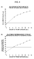
- Part (a) of Fig. 4 is a graph illustrating the relationship between the amount of pre-nip exposure and a direct-current current flowing between the photoconductor drum 1 and the charging roller 2. Further, part (b) of Fig. 4 is a graph illustrating the relationship between a direct-current current flowing between the photoconductor drum 1 and the charging roller 2 and the amount of scraping of the photoconductor drum 1 when 10,000 (10K) A4 size sheets having solid white images (0 in 255 grayscale levels) over the entirety thereof are output. Specifically, in Fig.
- the process speed is 210 mm/s
- the charging potential is -500 V
- solid-white printing endurance is measured
- the DC current value is measured using an ammeter provided between the photoconductor drum 1 and a ground.
- pre-nip exposure be performed with the amount of light corresponding to the process speed in order to prolong the life of the photoconductor drum 1 while suppressing formation of a charging lateral stripe.
- Fig. 5 is a flowchart describing the operation of the image forming apparatus according to the exemplary embodiment.
- the CPU in the control circuit controls the image forming apparatus in accordance with a program stored in the ROM to operate in the manner as in the flowchart described in Fig. 5 .
- the description will be given of an example in which image forming conditions are changed in accordance with the type of a sheet on which an image is to be formed. It is assumed that a user has specified the type of a sheet on which an image is to be formed using the operation panel.
- S101 is a step in which the control circuit 200 serving as control means obtains the type of a sheet on which an image is to be formed.
- the control circuit 200 obtains the type of the sheet set on the operation panel 100.
- S102 is a step for changing the process in accordance with the type of the sheet on which an image is to be formed.
- the control circuit 200 executes the processing of S103.
- the control circuit 200 executes the processing of S104.
- S103 is a step for setting image forming conditions when an image is to be formed on plain paper.
- the control circuit 200 sets the process speed for which an image is to be formed on plain paper to 210 mm/s and the amount of pre-nip exposure to 7 lx.s (first light amount).
- S104 is a step for setting image forming conditions when an image is to be formed on thick paper.
- the control circuit 200 sets the process speed for which an image is to be formed on thick paper to 105 mm/s and the amount of pre-nip exposure to 15 lx ⁇ s (second light amount).
- the control circuit 200 controls the image forming apparatus in accordance with the image forming conditions set in S103 or S104. Specifically, during image formation in which an image is formed on a sheet, the control circuit 200 drives the photoconductor drum 1 and the like to rotate to achieve the set process speed. Further, control is performed so that the pre-nip exposure device 8 can perform exposure at the desired amount of light to apply the desired charge bias to the charging roller 2.
- the control circuit 200 changes the amount of pre-nip exposure in accordance with the process speed. That is, as described above, a configuration is provided so that when the process speed is low, the amount of pre-nip exposure can be made large. With this configuration, the occurrence of a charging lateral stripe, which occurs when the photoconductor drum 1 is charged by the charging roller 2 is suppressed. That is, even when the process speed is changed depending on the type of the sheet on which an image is to be formed, the occurrence of an image defect caused by a charging lateral stripe can be suppressed. It is preferable that pre-nip exposure be performed when a portion of the photoconductor drum on which an electrostatic image corresponding to an image to be formed on a sheet is to be formed is charged.
- changing the power to be supplied to the pre-nip exposure device 8 from the power source S4 changes the amount of light radiated to the upstream-side charging gap by the pre-nip exposure device 8.
- changing the distance between the pre-nip exposure device and the upstream-side charging gap may also change the amount of light radiated to the upstream-side charging gap. That is, when the process speed is low, bringing the pre-nip exposure device 8 in closer proximity to the upstream-side charging gap than that when the process speed is high may increase the amount of light radiated to the upstream-side charging gap.
- a deflecting plate capable of adjusting light radiated to the upstream-side charging gap by the pre-nip exposure device 8 may also be provided.
- the amount of light radiated to the upstream-side charging gap is adjusted using a reflecting mirror serving as a reflecting member. Since exposure of the upstream-side charging gap to light is performed using the reflecting mirror, the reflecting mirror also corresponds to irradiation means.
- a configuration is adopted in which a light source of pre-exposure for removing residual electric charge that remains on the photoconductor drum after transfer and a light source of pre-nip exposure for suppressing the occurrence of a charging lateral stripe are commonly used.
- a light source for removing residual electric charge on the photoconductor drum and a light source of pre-nip exposure may be provided separately.
- the light source for removing residual electric charge on the photoconductor drum corresponds to erasing means.
- the higher the process speed of the photoconductor drum 1 the larger the amount of light radiated in order to erase residual electric charge on the photoconductor drum after transfer.
- the higher the process speed the smaller the amount of light required for the charging nip.
- light from a single light source is distributed to an upstream-side charging gap and a pre-exposure unit to remove residual electric charge and suppress the occurrence of a charging lateral stripe.
- a pre-exposure unit to remove residual electric charge and suppress the occurrence of a charging lateral stripe.
- a pre-nip exposure device that emits light at a constant light amount and a reflecting mirror whose position is finely adjusted by a motor are used to remove residual electric charge on the photoconductor drum and to suppress formation of a charging lateral stripe.
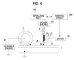
- Fig. 6 is a diagram describing the configuration of an apparatus that exposes a charging gap and a pre-exposure unit to light.
- a power source S4 supplies constant power to a pre-nip exposure device 8.
- the pre-nip exposure device 8 continues to output light at a constant light amount.
- the pre-nip exposure device 8 serving as a light source is provided to face the surface of the photoconductor drum 1, and a reflecting mirror 21 serving as irradiation means is disposed between the pre-nip exposure device 8 and the photoconductor drum 1.
- a motor finely adjusts the position of the reflecting mirror 21 serving as irradiation means.
- the reflecting mirror 21 reflects a laser beam L output from the pre-nip exposure device 8, thereby directing the laser beam L1 to an upstream-side charging gap.
- a laser beam L2 that is not reflected by the reflecting mirror 21 is radiated to the photoconductor drum 1. Therefore, electric charge (residual electric charge) that remains on the photoconductor drum after a toner image formed on the photoconductor drum 1 is transferred can be erased.
- the laser beam L2 reflected by the reflecting mirror 21 erases an image forming region in the longitudinal direction of the photoconductor drum 1.
- the power source S4 supplies power so that the pre-nip exposure device 8 can emit light at 20 1x ⁇ s.
- a motor 20 finely adjusts the position of the reflecting mirror 21.
- the laser beam L1 is 7 lx-s (first light amount) and the laser beam L2 is 13 lx-s (third light amount).
- the laser beam L1 is 15 lx-s (second light amount) and the laser beam L2 is 5 lx-s (fourth light amount).
- a pre-exposure device serving as removing means for removing residual electric charge may be provided separately from an inter-nip exposure device.
- a control circuit serving as control means performs control so that the pre-exposure device can remove residual electric charge on the photoconductor drum at 13 lx-s (third light amount) when the process speed is 210 mm/s. Further, the control circuit performs control so that the pre-exposure device can remove residual electric charge on the photoconductor drum at 5 lx-s (fourth light amount) when the process speed is 105 mm/s.
- the laser beam L2 serving to erase residual electric charge is radiated to the photoconductor drum 1.
- a developing device develops an electrostatic image formed on the photoconductor drum 1 and then a toner image is transferred onto a sheet serving as a transfer target member, residual electric charge on the photoconductor drum 1 can be removed.
- Exposure to the laser beam L2 serving to remove the residual electric charge is performed for a period from when the toner image is transferred onto the sheet at the transfer portion to when the toner image is conveyed to the upstream-side gap portion.
- a control circuit 200 includes a CPU, a RAM, etc., and controls individual units of the image forming apparatus in accordance with an image forming signal input from an operation panel 100 serving as an operation unit or an external terminal such as a PC.
- the motor 20 can cause the reflecting mirror 21 to move to the position (i) or (ii) in accordance with the input from the control circuit 200.
- Fig. 7 is a flowchart illustrating the operation of the image forming apparatus according to the exemplary embodiment.
- the description will be given of an example in which image forming conditions are changed in accordance with the type of a sheet on which an image is to be formed.
- S201 is a step in which the control circuit 200 serving as control means obtains the type of a sheet on which an image is to be formed.
- the control circuit 200 obtains the type of the sheet set on the operation panel 100.
- S202 is a step for changing the process in accordance with the type of the sheet on which an image is to be formed.
- the control circuit 200 executes the processing of S203.
- the control circuit 200 executes the processing of S204.
- S203 is a step for setting image forming conditions when an image is to be formed on plain paper.
- the control circuit 200 sets the process speed for which an image is to be formed on plain paper to 210 mm/s and the position of the reflecting mirror 21 to (i).
- S204 is a step for setting image forming conditions when an image is to be formed on thick paper.
- the control circuit 200 sets the process speed for which an image is to be formed on thick paper to 105 mm/s and the position of the reflecting mirror 21 to (ii).
- the control circuit 200 controls the image forming apparatus in accordance with the image forming conditions set in S203 or S204. Specifically, the control circuit 200 drives the photoconductor drum 1 and the like to rotate to achieve the set process speed. Further, the motor 20 is controlled so that the reflecting mirror 21 can be located at the desired position to apply the desired charge bias to the charging roller 2.
- the control circuit 200 changes the position of the reflecting mirror 21 in accordance with the process speed. That is, a configuration is provided so that when the process speed is low, the amount of pre-nip exposure can be large and the amount of pre-exposure can be small.
- This configuration can remove residual electric charge on the photoconductor drum 1 while suppressing the occurrence of a charging lateral stripe which occurs when the charging roller 2 charges the photoconductor drum 1. That is, even when the process speed is changed depending on the type of the sheet on which an image is to be formed, light sources can be commonly used while the occurrence of an image defect caused by a charging lateral stripe is suppressed.
- adjusting the position of the reflecting mirror 21 achieves the erasure of residual electric charge and the suppression of occurrence of a charging lateral stripe.
- a half-mirror type variable transmittance element (a mirror whose reflectance and transmittance are changed by applying a voltage) serving as a reflecting member capable of adjusting the amount of reflection and the amount of transmission of light may be used.
- a half-mirror type variable transmittance element in place of the reflecting mirror 21, it is not necessary to move the reflecting mirror 21.
- an upstream-side charging gap can be exposed to light at a higher accuracy than that when a mirror is moved using a motor.
- an image forming apparatus forms an image at a process speed determined in advance in accordance with the type of sheet.
- LEDs are adopted as a pre-nip exposure device and a pre-exposure device, other exposure devices such as a light irradiation device including a fuse lamp may also be used.
- an upstream-side charging gap may be exposed to light from inside a transparent photosensitive member.
- the charging roller 2 serving as a flexible contact charging member, by way of example.
- similar benefits can be expected, as long as the distance of the upstream-side charging gap decreases and the distance of the downstream-side charging gap increases, regardless of whether the distance between the charging member and the photosensitive member increases linearly or non-linearly.
- a conductive charging belt, a conductive rubber blade that is brought into abutment against the photosensitive member at the edge portions to charge the photosensitive member, or the like may be used as a charging member.
- the charging roller 2 serving as a charging member and the photoconductor drum 1 serving as a photoconductor are in contact with each other, a small gap may be formed.
- the distance between the photoconductor drum 1 and the charging roller 2 decreases toward the position where the charging roller 2 and the photoconductor drum 1 are the closest to each other in the rotation direction of the photoconductor drum 1.
- the rotatable drum-shaped photoconductor drum 1 is used.
- a movable belt-shaped photosensitive belt may be used as a photosensitive member. In this case, it is assumed that the upstream and downstream in the rotation direction of the photoconductor drum 1 correspond to the upstream and downstream in the movement direction of the photosensitive belt, respectively.
- an entire longitudinal area of the photoconductor drum 1 may be exposed to light. This can suppress the occurrence of non-uniformity in the amount of scraping in the longitudinal direction of the photoconductor drum 1 when an apparatus that forms an image on a small sheet and a large sheet continues to form an image on small paper.
- a known media sensor may be used to specify a sheet on which an image is to be formed.
- an image forming apparatus having the so-called cleanerless configuration in which developing and cleaning are simultaneously performed using a developing device can also be used.
Landscapes
- Physics & Mathematics (AREA)
- General Physics & Mathematics (AREA)
- Engineering & Computer Science (AREA)
- Plasma & Fusion (AREA)
- Microelectronics & Electronic Packaging (AREA)
- Health & Medical Sciences (AREA)
- Toxicology (AREA)
- Electrostatic Charge, Transfer And Separation In Electrography (AREA)
- Control Or Security For Electrophotography (AREA)
- Discharging, Photosensitive Material Shape In Electrophotography (AREA)
Abstract
Description
- The present invention relates to an electrophotographic image forming apparatus such as a copying machine, a printer, or a FAX.
- Recent electrophotographic image forming apparatuses use a method for, in order to charge a photosensitive member, bringing a roller or blade charging member into contact with the photosensitive member to charge the photosensitive member. Two methods are well known to charge a photosensitive member by using a contact charging method. The first method is an "AC charging method" in which a superimposed voltage of direct-current voltage and alternating-current voltage is applied to a charging member to charge a photosensitive member, and the second method is a "DC charging method" in which only a direct-current voltage is applied to a charging member to charge a photosensitive member. Due to the application of an alternating-current voltage, the "AC charging method" allows a more uniform charging of the surface of a photosensitive member than the "DC charging method". In the "AC charging method", on the other hand, the amount of discharge to the photosensitive member is larger than that in the "DC charging method", and therefore the surface of the photosensitive member is more easily scraped. Thus, if a photosensitive member is charged using the "AC charging method", the life of the photosensitive member will be shorter than that when the photosensitive member is charged using the "DC charging method". Further, the "AC charging method" requires an AC power source. Thus, the "AC charging method" has a greater initial cost and a higher running cost than that required for the "DC charging method". In other words, the "DC charging method" is more advantageous than the "AC charging method" in terms of running cost and initial cost. However, the uniformity of surface potential of a photosensitive member (charging uniformity) is lower in the "DC charging method" than the charging uniformity in the "AC charging method". Specifically, there has arisen a problem of stripe-shaped charging non-uniformity (charging lateral stripe) in the longitudinal direction (direction perpendicular to the circumferential direction) of an electrophotographic photosensitive member, which is caused by the non-uniform surface potential of the photosensitive member. Presumably, this is caused by the occurrence of separating discharge in a charging gap (fine gap) located downstream in the rotation direction of a photosensitive drum, between the photosensitive member that is charged in a charging gap located upstream in the rotation direction of the photosensitive drum and a charging roller.
- Thus, a configuration for suppressing formation of a "charging lateral stripe" that occurs when a photosensitive member is charged using the "DC charging method" is disclosed in
PTL 1. Specifically, among charging gaps produced by bringing a charging roller and a photosensitive drum into contact with each other, a charging gap located upstream in the rotation direction of the photosensitive member is irradiated with light (pre-nip exposure). Therefore, the charge of the photosensitive member is canceled in the charging gap located upstream, and the photosensitive member is charged in a charging gap located downstream in the rotation direction of the photosensitive member. In turn, this suppresses the occurrence of a charging lateral stripe caused by separating discharge. -
- PTL 1: Japanese Patent Laid-Open No.
5-341626 - Meanwhile, there has been an increasing demand for electrophotographic devices adapted to form images on a variety of media. A configuration for forming images on various media by changing the process speed depending on the type of the medium has been widely adopted. When a toner image is fixed onto paper having a relatively high basis weight (hereinafter referred to as thick paper), a large amount of heat is required to guarantee fixing properties equivalent to those when a toner image is fixed onto plain paper (paper having basis weight of approximately 50 to 100 mg/m2). Thus, a configuration in which when an image is to be formed on paper of high basis weight, the fixing speed of a fixing device is reduced to increase the heating time to give a large amount of heat to the paper is known. Many image forming apparatuses further adopt a configuration in which the process speed of a photosensitive member is also reduced as, and in the same manner as, the fixing speed of the fixing device is reduced.
- In this manner, an apparatus having a photosensitive member that moves at each process speed has had a problem in that a charging lateral stripe occurs if a charging gap located upstream in the rotation direction of the photosensitive member is irradiated with constant light regardless of the process speed (rotational speed of the photosensitive member). Specifically, when an image is to be formed on plain paper, a charging lateral stripe occurs if the charging gap located upstream is exposed to light at an amount that is equal to the amount of light exposed to a charging gap located upstream when an image is to be formed on thick paper. Presumably, this is caused by the occurrence of separating discharge in a charging gap located downstream because if the process speed is low, the photosensitive member is sufficiently charged in the charging gap located upstream even when the charging gap located upstream is subjected to erasure with light.
- In order to solve the above problems, the present invention provides an image forming apparatus including a rotatable photosensitive member, a charging member that is in contact with the photosensitive member to charge the photosensitive member, a power source that applies a direct-current voltage to the charging member, and irradiation means for irradiating a charging gap located upstream in a rotation direction of the photosensitive member with light among charging gaps at which the charging member charges the photosensitive member, wherein the image forming apparatus further includes control means for controlling the irradiation means to irradiate the charging gap located upstream with light of a first light amount when the photosensitive member rotates at a first speed, and to irradiate the charging gap located upstream with light of a second light amount that is larger than the first light amount when the photosensitive member rotates at a second speed that is lower than the first speed.
- In an image forming apparatus in which applying a direct-current voltage to a charging member charges a photosensitive member, the occurrence of a charging lateral stripe can be suppressed even when the rotational speed of the photosensitive member is changed.
-
- [
Fig. 1] Fig. 1 includes diagrams describing the schematic configuration of an image forming apparatus according to an exemplary embodiment, the layer configuration of a photoconductor drum, and the layer configuration of a charging roller. - [
Fig. 2] Fig. 2 is a schematic configuration diagram illustrating an operation unit of the image forming apparatus according to the exemplary embodiment. - [
Fig. 3] Fig. 3 is a block diagram of the image forming apparatus according to the exemplary embodiment. - [
Fig. 4] Fig. 4 includes graphs illustrating the relationship between the amount of pre-nip exposure and the value of current flowing between the charging roller and the photoconductor drum in the image forming apparatus according to the exemplary embodiment, and illustrating the relationship between the value of the current and the amount of scraping of the photoconductor drum. - [
Fig. 5] Fig. 5 is a flowchart describing the operation of the image forming apparatus according to the exemplary embodiment. - [
Fig. 6] Fig. 6 is a block diagram of the image forming apparatus according to the exemplary embodiment. - [
Fig. 7] Fig. 7 is a flowchart describing the operation of the image forming apparatus according to the exemplary embodiment. - [
Fig. 8] Fig. 8 includes diagrams describing the pre-nip exposure and the deviation of discharge caused by changing of the process speed. - A configuration for carrying out the present invention will be described hereinafter with respect to an example thereof. It is to be noted that the present invention is not to be limited to the following configuration unless otherwise specified.
Exemplary Embodiment 1 - The configuration of an image forming apparatus according to the exemplary embodiment will be described hereinafter.
-
Fig. 1 includes schematic diagrams describing the overall configuration of an image forming apparatus. As illustrated in part (a) ofFig. 1 , an image forming apparatus according to the exemplary embodiment is an electrophotographic image forming apparatus that uses a roller charging device to charge a photosensitive drum. More specifically, the image forming apparatus is a laser beam printer capable of forming an image on paper up to A3 size, which adopts a contact charging method in which a charging roller is brought into contact with the photosensitive drum and a reversal developing method in which a region where a toner image is to be formed is exposed to light. In the embodiment, aphotoconductor drum 1 that is a drum-shaped photosensitive member is a negative chargeable organic photoconductor (OPC) with an outer diameter of 30 mm, and is caused to rotate by a driving force from a motor (not illustrated) serving as a driving device. Here, thephotoconductor drum 1 is driven to rotate in the arrow direction (counterclockwise) at a peripheral speed (hereinafter referred to as a process speed) of 210 mm/s when an image is to be formed on plain paper, and at a peripheral speed of 105 mm/s when an image is to be formed on thick paper. As illustrated in part (b) ofFig. 1 , thephotoconductor drum 1 is configured by coating a surface of an aluminum cylinder (conductive drum base) 1a with three layers of an undercoatinglayer 1b for improving adhesiveness of upper layers while reducing optical interference, a photocharge generatinglayer 1c, and acharge transport layer 1d in order from the bottom. In the image forming apparatus, acharging roller 2 serving as a charging member, which is in contact with thephotoconductor drum 1, a developingdevice 4, atransfer roller 5, and acleaning device 7 are arranged around thephotoconductor drum 1 along the rotation direction (counterclockwise) thereof. Further, anexposure device 3 serving as electrostatic image forming means is provided above thephotoconductor drum 1 between thecharging roller 2 and the developingdevice 4. Afixing device 6 is provided downstream in a transfer material conveying direction of a transfer portion d formed by thephotoconductor drum 1 and thetransfer roller 5. Each configuration will be described in detail hereinafter along with steps of the image forming apparatus. - The
charging roller 2 that charges thephotoconductor drum 1 is held in a rotatable manner at both ends of acore metal 2a by bearing members (not illustrated). Apressure spring 2e urges thecharging roller 2 toward the center of thephotoconductor drum 1 so that thecharging roller 2 is pressed against the surface of thephotoconductor drum 1 with a predetermined pressing force. Thecharging roller 2 rotates in accordance with the rotational driving of thephotoconductor drum 1. Thephotoconductor drum 1 and thecharging roller 2 are brought into contact with each other to form a contact portion. The gap between thephotoconductor drum 1 and thecharging roller 2 increases in the rotation direction of the photosensitive member from the contact portion. Here, the pressed portion (contact portion) between thephotoconductor drum 1 and the chargingroller 2 is referred to as a charging nip portion. A fine gap located upstream the pressed portion in the rotation direction of thephotoconductor drum 1 is referred to as an upstream-side charging gap A1. Similarly, a fine gap located downstream the pressed portion in the rotation direction of thephotoconductor drum 1 is referred to as a downstream-side charging gap A2. Thephotoconductor drum 1 is charged in the upstream-side charging gap A1 and the downstream-side charging gap A2 with respect to the pressed portion. The charging of thephotoconductor drum 1 is performed by discharging from the chargingroller 2 to thephotoconductor drum 1. Thus, a voltage greater than or equal to a threshold voltage at which discharge starts is applied to the chargingroller 2. In the exemplary embodiment, when a voltage greater than or equal to about -600 V is applied to the chargingroller 2, the surface potential of the photosensitive member starts to increase. The surface potential of thephotoconductor drum 1 increases after the application of about -600 V while keeping substantially the linear relationship with applied voltages. In the image forming apparatus of the exemplary embodiment, if -900 V is applied to the chargingroller 2, the surface of thephotoconductor drum 1 reaches -300 V. Further, if -1100 V is applied to the chargingroller 2, the surface of thephotoconductor drum 1 reaches -500 V. This threshold voltage (-600 V) is hereinafter referred to as a discharge start voltage (charging start voltage) Vth (V). That is, in an electrophotographic image forming process, it is necessary to apply Vd+Vth (V) to the chargingroller 2 to charge the potential on the surface of thephotoconductor drum 1 to Vd (V) (dark potential). In other words, a voltage of Vd+Vth (V) is applied to thecore metal 2a of the chargingroller 2 by a power source S1, thus allowing the potential on the surface of thephotoconductor drum 1 to reach Vd (V). In the image forming apparatus of the exemplary embodiment, in order to form an image, the dark potential Vd is set to -500 V when thephotoconductor drum 1 is charged. Thus, during image formation, a direct-current voltage (hereinafter referred to as a DC bias) of -1100 V is applied to the chargingroller 2 from the direct-current power source S1. Here, the width of the charging gap in the photosensitive drum direction at which the charging roller charges thephotoconductor drum 1 by discharging changes depending on the voltage applied to the charging roller. That is, while a charging gap refers to a portion where the photoconductor drum is charged by the occurrence of discharging, it is known that a fine gap in which a discharge occurs when a voltage is applied changes in accordance with Paschen's law. Note that a portion where thephotoconductor drum 1 is charged when a bias is applied to the chargingroller 2 in the state where the rotation of thephotoconductor drum 1 is stopped corresponds to a charging gap. - Subsequently, the charging
roller 2 will be described in detail. The longitudinal length of the chargingroller 2 is 320 mm. As illustrated in part (b) ofFig. 1 , the chargingroller 2 has a three-layer configuration in which alower layer 2b, an intermediate layer 2c, and asurface layer 2d are stacked in this order around the core metal (supporting member) 2a. Thelower layer 2b is a foamed sponge layer for reducing charging sound. Further, thesurface layer 2d acts as a protective layer for preventing leakage of current even if thephotoconductor drum 1 has a defect thereon such as a pinhole. Thecore metal 2a is a stainless round bar with a diameter of 6 mm. Further, thelower layer 2b is composed of foamed EPDM with carbon dispersed therein with a thickness of 3.0 mm. Note that foamed EPDM having a specific gravity of 0.5 g/cm3 and a volume resistance of 102 to 109 Ωcm is used. The intermediate layer 2c is composed of NBR-based rubber with carbon dispersed (a volume resistance of 102 to 105 Ωcm) with a thickness of 700 µm. Thesurface layer 2d is formed of Toresin resin, which is a fluorinated compound, with a thickness of 10 µm. Note that Toresin resin with tin oxide and carbon dispersed therein and having a volume resistance of 107 to 1010 Ωcm is used. Further, the surface roughness of the charging roller 2 (10-point average surface roughness Ra in JIS) is 1.5 µm. - The
exposure device 3 serving as electrostatic image forming means for forming an electrostatic image on the chargedphotoconductor drum 1 will be described. In the exemplary embodiment, theexposure device 3 is a laser beam scanner using a semiconductor laser. Theexposure device 3 outputs a laser beam that is modulated in accordance with an image signal input from a host processor such as an image reading device (not illustrated). The laser beam is scanned at an exposure position b on the surface of the chargedphotoconductor drum 1, and an electrostatic image corresponding to the input image signal is formed on the photoconductor drum 1 (on the photosensitive member). - Subsequently, a developing step will be described. The developing
device 4 develops the electrostatic image formed on thephotoconductor drum 1. In the image forming apparatus in the exemplary embodiment, a two-component developer is used, and an electrostatic image is developed using a magnetic brush. In the exemplary embodiment, since the image forming apparatus adopts the reversal developing method, the electrostatic image is developed by attaching toner to an exposed portion (bright portion) of the surface of thephotoconductor drum 1. The configuration of the developingdevice 4 will be described in detail hereinafter. The developingdevice 4 includes a developingcontainer 4a, and a rotatable non-magnetic developingsleeve 4b disposed at an opening of the developing container, which includes a fixedmagnet roller 4c. To coat thesleeve 4b with a thin layer of developer, aregulating blade 4d regulates adeveloper 4e containing toner and carrier (magnetic particles), which is accommodated in the developingcontainer 4a, to obtain a certain thickness. On the developingsleeve 4b serving as a developer carrying member, the internal magnet causes the magnetic brush to be erected by the carrier, and the toner is conveyed to a developing portion c where the developingsleeve 4b faces thephotoconductor drum 1. Thedeveloper 4e in the developingcontainer 4a is a mixture of toner and magnetic carrier. Thedeveloper 4e is conveyed toward the developingsleeve 4b while being stirred uniformly by the rotation of twodeveloper stirring members 4f (stirring screws). In the embodiment, the magnetic carrier has a resistance of about 1013 Ωcm and a particle diameter of about 40 µm. The toner is rubbed with the magnetic carrier and is therefore frictionally charged to the negative polarity. In addition, a density sensor (not illustrated) detects the toner density in the developingcontainer 4a. Moreover, the toner is replenished into the developingcontainer 4a from atoner hopper 4g based on detection information detected by the density sensor so that the toner density in the developing container can be made uniform. The developingsleeve 4b is provided to face thephotoconductor drum 1 in close proximity thereto while keeping the closest distance at the developing portion c from thephotoconductor drum 1 at 300 µm. In addition, the developingsleeve 4b is driven to rotate in the direction opposite to the rotation direction (counterclockwise) of thephotoconductor drum 1 at the developing portion c. Further, a predetermined developing bias is applied to the developingsleeve 4b from a power source S2. In the exemplary embodiment, a developing bias in which a direct-current voltage (Vdc) and an alternating-current voltage (Vac) are superimposed is applied to the developingsleeve 4b. Specifically, the frequency of the alternating-current voltage is 8 kHz, the direct-current voltage is -320 V, and the peak-to-peak voltage Vpp of the alternating-current voltage is 1800 V. - A toner image formed on the
photoconductor drum 1 through the developing step is transferred onto a sheet in a transfer step. Thetransfer roller 5 abuts against thephotoconductor drum 1 with a predetermined pressing force to form the transfer portion d. Further, a transfer bias (positive transfer bias having a polarity that is opposite to the normal charged polarity of the toner, i.e., negative polarity; in the embodiment, +500 V) is applied to thetransfer roller 5 from a power source S3. Therefore, the toner image on the surface of thephotoconductor drum 1 is transferred onto a sheet conveyed to the transfer portion d. Thecleaning device 7 cleans toner that is not transferred onto the sheet from thephotoconductor drum 1. In the exemplary embodiment, thecleaning device 7 includes acleaning blade 7a. Untransferred residual toner that is still attached to thephotosensitive drum 1 is contacted with thecleaning blade 7a and is therefore removed. In part (a) ofFig. 1 , reference numeral e denotes a photosensitive drum surface abutting portion of thecleaning blade 7a. - Subsequently, a fixing step of fixing the toner image transferred onto the sheet in the transfer portion d will be described. The fixing
device 6 that fixes a toner image onto a sheet includes arotatable fixing roller 6a and apressure roller 6b. In a fixing nip portion formed by the fixingroller 6a and thepressure roller 6b, the fixingdevice 6 fixes the toner image transferred onto the sheet by heating and pressing the toner image while conveying the sheet that is being held therebetween. In the exemplary embodiment, a control circuit controls the rotational speeds of the fixingroller 6a and the pressure roller 6bin accordance with the material, thickness, basis weight, etc. of the sheet. Specifically, the fixingroller 6a and thepressure roller 6b rotate so that the process speed can reach 105 mm/s when an image is to be fixed onto thick paper (having basis weight of 101 to 200 g/m2). Further, the fixingroller 6a and thepressure roller 6b rotate so that the process speed can reach 210 mm/s when an image is to be fixed onto plain paper (havingbasis weight 50 to 100 g/m2). - Subsequently, an operation panel unit in the image forming apparatus will be described.
Fig. 4 includes diagrams describing an operation panel. Part (a) ofFig. 4 is a diagram describing the outer appearance of anoperation panel 100. Theoperation panel 100 includes astart button 101 for allowing the image forming apparatus to execute image formation based on set information. Theoperation panel 100 further includes a touch-panel display 102. A screen as illustrated in part (b) ofFig. 2 is displayed on thedisplay 102. A user can select a button displayed on thedisplay 102 to perform various settings for image formation. In the exemplary embodiment, in particular, the setting of the type of a sheet on which an image is to be formed and a quality priority mode will be described in detail. In part (b) ofFig. 2 ,reference numeral 103 denotes a button for setting the type of a sheet on which an image is to be formed. Whenreference numeral 103 is selected, a screen in part (c) ofFig. 2 is displayed on thedisplay 102. In part (c) ofFig. 2 , a list of sheets available for image formation is displayed. A user can select one ofplain paper 104,thick paper 105, coated paper, and the like in accordance with the type of the sheet to be used for image formation. As described above, when theplain paper 104 is selected, the process speed is set to 210 mm/s. Further, when thethick paper 105 is selected, the process speed is set to 105 mm/s. Coated paper is a glossy sheet whose surface smoothness is improved by coating the surface of the sheet with a transparent resin. When an image is to be formed on coated paper, as with thick paper, the process speed is also set to 105 mm/s. The type of the sheet may not necessarily be set by a user but may be determined using a sensor or the like. In part (b) ofFig. 2 ,reference numeral 104 denotes a button for specifying a high-quality mode. With the use of this button, when an image is to be formed on plain paper, the process speed is also changed to 105 mm/s. The reduction of the process speed allows an electrostatic image having a higher resolution than that at a high process speed to be formed on thephotoconductor drum 1. - When the
start button 101 is pressed after the paper type, mode, etc. are set, the image forming apparatus forms an image in accordance with the set conditions. A printing instruction may also be input from an external terminal such as a PC. - A pre-nip exposure device serving as irradiation means for radiating light in order to suppress formation of a charging lateral stripe will be described hereinafter.
Fig. 3 is a diagram describing a pre-nip exposure device that exposes a charging gap to light. Applying a direct-current voltage from the power source S1 to the chargingroller 2 charges thephotoconductor drum 1. Further, a power source S4 supplies power to apre-nip exposure device 8 in accordance with the control of acontrol circuit 200. Thepre-nip exposure device 8 radiates light to an upstream-side charging gap in the rotation direction of thephotoconductor drum 1. More specifically, thepre-nip exposure device 8 exposes the upstream-side charging gap in the rotation direction of thephotoconductor drum 1 to light from a nip portion between thephotoconductor drum 1 and the chargingroller 2, and an image forming region is erased in the longitudinal direction of thephotoconductor drum 1. In the exemplary embodiment, an LED (Light Emitting Diode) having a peak wavelength of 660 (± 10) nm at a room temperature (20°C) is used as thepre-nip exposure device 8. It is known that the wavelength of emitted light changes depending on the temperature of the material and the applied current. In the exemplary embodiment, an LED having a forward drop voltage of 1.4 V, a maximum rated output of 3 mW, a maximum operating current of 95 mA, a maximum output of 2.1 mW, and a luminous efficiency of 39 lm/W is used. A multiple number of such LEDs are arranged side-by-side, and an LED driver applies a PWM (Pulse Width Modulated) voltage to the LEDs to allow control of the light amount of the pre-nip exposure device. Note that the upstream-side charging gap refers to a small region where discharge is performed between the chargingroller 2 and thephotoconductor drum 1. In the exemplary embodiment, the upstream-side charging gap A1 is a region that is located 1 mm away upstream in the rotation direction of thephotoconductor drum 1 from the nip portion between thephotoconductor drum 1 and the chargingroller 2. Likewise, the downstream-side charging gap A2 is a region that is located 1 mm away downstream in the rotation direction of thephotoconductor drum 1 from the nip portion between thephotoconductor drum 1 and the chargingroller 2. - The
control circuit 200 serving as control means includes a CPU, a RAM, etc., and controls individual units of the image forming apparatus in accordance with an image forming signal input from theoperation panel 100 serving as an operation unit or an external terminal such as a PC. For example, thecontrol circuit 200 obtains information or the like about a sheet specified using theoperation panel 100, and determines the process speed accordingly. Further, thecontrol circuit 200 controls the image forming condition of each image forming unit in accordance with the process speed. Specifically, by way of example, thecontrol circuit 200 is capable of controlling power to be supplied to thepre-nip exposure device 8 from the power source S4. In accordance with the power supplied from the power source S4 serving as feeding means, thepre-nip exposure device 8 can output light of 0 to 15 1x·s per unit time. Note that the light amount is measured using an illuminometer that conforms to general class AA of JIS C 1609-1 (revised 2006). The illuminometer measures the light amount in a visible light region (420 to 700 nm). Thus, for example, a photodiode may be used to detect a change in the light amount in a region other than the visible light region. In order to detect a change in the light amount in the wavelength at which the electric charge on the surface of the photosensitive member can be removed, preferably, a photodiode detects light transmitted through an optical filter that cuts the wavelength to which the photosensitive member is less sensitive. - The case where the light amount of pre-nip exposure is made constant regardless of the process speed will be described hereinafter.
Fig. 8 includes schematic diagrams describing a separating discharge phenomenon that occurs in thephotoconductor drum 1 when the upstream-side charging gap in the rotation direction of thephotoconductor drum 1 is exposed to light with a constant light amount in order to suppress formation of a charging lateral stripe. Part (a) ofFig. 8 is a schematic diagram of the upstream-side charging gap exposed to light when the process speed is 210 mm/s. Further, part (b) ofFig. 8 is a schematic diagram of the upstream-side charging gap exposed to light with a light amount (7 1x·s), which is the same as that when the process speed is 210 mm/s, when the process speed is 105 mm/s. - First, the case where pre-gap exposure is not performed will be described. The charging
roller 2 rotates forward relative to thephotoconductor drum 1 that is rotating, and thephotoconductor drum 1 is charged. In the upstream-side charging gap A1, when the potential difference between thephotoconductor drum 1 and the chargingroller 2 exceeds a discharge start threshold (based on Paschen's law), discharge is performed, and thephotoconductor drum 1 is charged to the charging potential (Vd). However, if the resistance of a portion of the chargingroller 2 is high or a portion of thephotoconductor drum 1 is thick, uniform charging may not be completed in the upstream-side charging gap A1. In this case, minute discharge occurs in the downstream-side charging gap A2, resulting in the occurrence of charging lateral stripe. Thus, as illustrated in part (a) ofFig. 8 , the upstream-side charging gap A1 is exposed to light to charge the photosensitive member at the downstream-side charging gap to suppress the occurrence of a charging lateral stripe. As illustrated in part (a) ofFig. 8 , a laser beam L produced by thepre-nip exposure device 8 subjects the chargedphotoconductor drum 1 to erasure in the upstream-side charging gap A1. Thus, thephotoconductor drum 1 is charged at the downstream-side charging gap A2. Thus, minute discharge is less likely to occur in the downstream-side charging gap A2, and the formation of a charging lateral stripe can be suppressed. - Subsequently, the case where erasure is performed at the upstream-side charging gap A1 with an amount of light, which is similar to that when the process speed is 210 mm/s, when the process speed is 105 mm/s will be described. Even when the upstream-side charging gap A1 is exposed to light with a similar light amount, the
photoconductor drum 1 is sufficiently charged at the upstream-side charging gap A1. That is, since thephotoconductor drum 1 is charged at the upstream-side charging gap A1, the minute discharging that occurs in the downstream-side charging gap A2 cannot be sufficiently suppressed. In other words, when an image is to be formed on thick paper, if pre-nip exposure is performed with the same light amount as that in the case of plain paper, output printed matter containing an image defect caused by a charging lateral stripe is observed. Therefore, in the exemplary embodiment, the image forming apparatus performs control to adjust the light amount of the pre-nip exposure device in accordance with the process speed. - The
control circuit 200 changes the process speed based on the information or the like about the sheet set using theoperation unit 100. As described above, if the upstream-side charging gap is exposed to light with a constant light amount regardless of the process speed, a charging lateral stripe is produced. Thus, the amount of light radiated to the charging gap is changed for each process speed, and an image defect caused by a charging lateral stripe that occurs in the current output printed matter is evaluated. - Table 1 is a table of evaluations for printed matter output with the amount of exposure changed when the process speeds are 210 mm/s (first speed) and 105 mm/s (second speed).
-
[Table 1] - Amount of exposure (lx·s) Process speed 5 7 9 11 13 15 105 (mm/s) × × × Δ ○ ⊙ 210 (mm/s) ○ ⊙ ⊙ ⊙ ⊙ ⊙ - A charging lateral stripe appears in a striped pattern in the direction parallel to the charging
roller 2, and noticeably appears when a halftone image is formed. Thus, printed matter in which a halftone (125 out of 255 grayscale levels) image is formed over an entire sheet is used. In Table 1, ⊙ is marked when the image on the output printed matter is good, ○ is marked when the image is fair, Δ is marked when density variation occurs, and × is marked when density variation or non-uniformity of density occurs. As can be seen from Table 1, the lower the process speed, the more the need for suppressing formation of a charging lateral stripe by increasing the amount of pre-nip exposure. - The amount of pre-nip exposure and the amount of scraping of the
photoconductor drum 1 will be described hereinafter. Part (a) ofFig. 4 is a graph illustrating the relationship between the amount of pre-nip exposure and a direct-current current flowing between thephotoconductor drum 1 and the chargingroller 2. Further, part (b) ofFig. 4 is a graph illustrating the relationship between a direct-current current flowing between thephotoconductor drum 1 and the chargingroller 2 and the amount of scraping of thephotoconductor drum 1 when 10,000 (10K) A4 size sheets having solid white images (0 in 255 grayscale levels) over the entirety thereof are output. Specifically, inFig. 4 , the process speed is 210 mm/s, the charging potential is -500 V, solid-white printing endurance is measured, and the DC current value is measured using an ammeter provided between thephotoconductor drum 1 and a ground. As can be seen from parts (a) and (b) ofFig. 4 , as the amount of light radiated to the charging gap (hereinafter referred to as the amount of pre-nip exposure) increases, the amount of scraping of thephotoconductor drum 1 increases. This is because as the amount of pre-nip exposure increases, the amount of erasure in the upstream charging gap between thephotoconductor drum 1 and the chargingroller 2 increases, resulting in an increase in redischarging for recharging thephotoconductor drum 1 from the chargingroller 2. Thus, for a high process speed (210 mm/s), irradiation with light at a light amount (15 lx·s), which is required to suppress formation of a charging lateral stripe on thephotoconductor drum 1 for a low process speed (105 mm/s), reduces the life of thephotoconductor drum 1. Therefore, it is preferable that pre-nip exposure be performed with the amount of light corresponding to the process speed in order to prolong the life of thephotoconductor drum 1 while suppressing formation of a charging lateral stripe. - The operation of the image forming apparatus for changing the amount of pre-nip exposure in accordance with the process speed will be described hereinafter with reference to a flowchart.
Fig. 5 is a flowchart describing the operation of the image forming apparatus according to the exemplary embodiment. The CPU in the control circuit controls the image forming apparatus in accordance with a program stored in the ROM to operate in the manner as in the flowchart described inFig. 5 . In the exemplary embodiment, the description will be given of an example in which image forming conditions are changed in accordance with the type of a sheet on which an image is to be formed. It is assumed that a user has specified the type of a sheet on which an image is to be formed using the operation panel. - S101 is a step in which the
control circuit 200 serving as control means obtains the type of a sheet on which an image is to be formed. Thecontrol circuit 200 obtains the type of the sheet set on theoperation panel 100. S102 is a step for changing the process in accordance with the type of the sheet on which an image is to be formed. When the type of the sheet on which an image is to be formed, which is obtained in S101, is plain paper, thecontrol circuit 200 executes the processing of S103. Further, when the type of the sheet on which an image is to be formed, which is obtained in S101, is thick paper, thecontrol circuit 200 executes the processing of S104. S103 is a step for setting image forming conditions when an image is to be formed on plain paper. Thecontrol circuit 200 sets the process speed for which an image is to be formed on plain paper to 210 mm/s and the amount of pre-nip exposure to 7 lx.s (first light amount). S104 is a step for setting image forming conditions when an image is to be formed on thick paper. Thecontrol circuit 200 sets the process speed for which an image is to be formed on thick paper to 105 mm/s and the amount of pre-nip exposure to 15 lx·s (second light amount). In S105, thecontrol circuit 200 controls the image forming apparatus in accordance with the image forming conditions set in S103 or S104. Specifically, during image formation in which an image is formed on a sheet, thecontrol circuit 200 drives thephotoconductor drum 1 and the like to rotate to achieve the set process speed. Further, control is performed so that thepre-nip exposure device 8 can perform exposure at the desired amount of light to apply the desired charge bias to the chargingroller 2. - In this manner, prior to image formation, the
control circuit 200 changes the amount of pre-nip exposure in accordance with the process speed. That is, as described above, a configuration is provided so that when the process speed is low, the amount of pre-nip exposure can be made large. With this configuration, the occurrence of a charging lateral stripe, which occurs when thephotoconductor drum 1 is charged by the chargingroller 2 is suppressed. That is, even when the process speed is changed depending on the type of the sheet on which an image is to be formed, the occurrence of an image defect caused by a charging lateral stripe can be suppressed. It is preferable that pre-nip exposure be performed when a portion of the photoconductor drum on which an electrostatic image corresponding to an image to be formed on a sheet is to be formed is charged. - In the exemplary embodiment, changing the power to be supplied to the
pre-nip exposure device 8 from the power source S4 changes the amount of light radiated to the upstream-side charging gap by thepre-nip exposure device 8. However, changing the distance between the pre-nip exposure device and the upstream-side charging gap may also change the amount of light radiated to the upstream-side charging gap. That is, when the process speed is low, bringing thepre-nip exposure device 8 in closer proximity to the upstream-side charging gap than that when the process speed is high may increase the amount of light radiated to the upstream-side charging gap. Further, a deflecting plate capable of adjusting light radiated to the upstream-side charging gap by thepre-nip exposure device 8 may also be provided. - Substantially the same portions as those in
Exemplary Embodiment 1 are assigned the same numerals and the descriptions thereof are thus omitted. In the exemplary embodiment, the amount of light radiated to the upstream-side charging gap is adjusted using a reflecting mirror serving as a reflecting member. Since exposure of the upstream-side charging gap to light is performed using the reflecting mirror, the reflecting mirror also corresponds to irradiation means. In the exemplary embodiment, a configuration is adopted in which a light source of pre-exposure for removing residual electric charge that remains on the photoconductor drum after transfer and a light source of pre-nip exposure for suppressing the occurrence of a charging lateral stripe are commonly used. It is to be understood that a light source for removing residual electric charge on the photoconductor drum and a light source of pre-nip exposure may be provided separately. In this case, the light source for removing residual electric charge on the photoconductor drum corresponds to erasing means. Here, it is preferable that the higher the process speed of thephotoconductor drum 1, the larger the amount of light radiated in order to erase residual electric charge on the photoconductor drum after transfer. Conversely, it is preferable that the higher the process speed, the smaller the amount of light required for the charging nip. Thus, in the exemplary embodiment, light from a single light source is distributed to an upstream-side charging gap and a pre-exposure unit to remove residual electric charge and suppress the occurrence of a charging lateral stripe. A configuration for removing residual electric charge and suppressing formation of a charging lateral stripe will be described hereinafter. - In the exemplary embodiment, a pre-nip exposure device that emits light at a constant light amount and a reflecting mirror whose position is finely adjusted by a motor are used to remove residual electric charge on the photoconductor drum and to suppress formation of a charging lateral stripe.
Fig. 6 is a diagram describing the configuration of an apparatus that exposes a charging gap and a pre-exposure unit to light. In the exemplary embodiment, a power source S4 supplies constant power to apre-nip exposure device 8. Thus, thepre-nip exposure device 8 continues to output light at a constant light amount. Thepre-nip exposure device 8 serving as a light source is provided to face the surface of thephotoconductor drum 1, and a reflectingmirror 21 serving as irradiation means is disposed between thepre-nip exposure device 8 and thephotoconductor drum 1. - A motor finely adjusts the position of the reflecting
mirror 21 serving as irradiation means. The reflectingmirror 21 reflects a laser beam L output from thepre-nip exposure device 8, thereby directing the laser beam L1 to an upstream-side charging gap. A laser beam L2 that is not reflected by the reflectingmirror 21 is radiated to thephotoconductor drum 1. Therefore, electric charge (residual electric charge) that remains on the photoconductor drum after a toner image formed on thephotoconductor drum 1 is transferred can be erased. The laser beam L2 reflected by the reflectingmirror 21 erases an image forming region in the longitudinal direction of thephotoconductor drum 1. Here, the power source S4 supplies power so that thepre-nip exposure device 8 can emit light at 20 1x·s. Further, amotor 20 finely adjusts the position of the reflectingmirror 21. When the reflectingmirror 21 is located at a position (i), the laser beam L1 is 7 lx-s (first light amount) and the laser beam L2 is 13 lx-s (third light amount). Further, when the reflectingmirror 21 is located at a position (ii), the laser beam L1 is 15 lx-s (second light amount) and the laser beam L2 is 5 lx-s (fourth light amount). - A pre-exposure device serving as removing means for removing residual electric charge may be provided separately from an inter-nip exposure device. In this case, a control circuit serving as control means performs control so that the pre-exposure device can remove residual electric charge on the photoconductor drum at 13 lx-s (third light amount) when the process speed is 210 mm/s. Further, the control circuit performs control so that the pre-exposure device can remove residual electric charge on the photoconductor drum at 5 lx-s (fourth light amount) when the process speed is 105 mm/s.
- That is, in either case, the laser beam L2 serving to erase residual electric charge is radiated to the
photoconductor drum 1. Thus, after a developing device develops an electrostatic image formed on thephotoconductor drum 1 and then a toner image is transferred onto a sheet serving as a transfer target member, residual electric charge on thephotoconductor drum 1 can be removed. Exposure to the laser beam L2 serving to remove the residual electric charge is performed for a period from when the toner image is transferred onto the sheet at the transfer portion to when the toner image is conveyed to the upstream-side gap portion. Similarly toExemplary Embodiment 1, acontrol circuit 200 includes a CPU, a RAM, etc., and controls individual units of the image forming apparatus in accordance with an image forming signal input from anoperation panel 100 serving as an operation unit or an external terminal such as a PC. Themotor 20 can cause the reflectingmirror 21 to move to the position (i) or (ii) in accordance with the input from thecontrol circuit 200. - The operation of the image forming apparatus for adjusting the amount of light radiated to the upstream-side charging gap and the amount of light with which pre-exposure is performed to remove residual electric charge on the photoconductor drum in accordance with the process speed will be described with reference to a flowchart.
Fig. 7 is a flowchart illustrating the operation of the image forming apparatus according to the exemplary embodiment. In the exemplary embodiment, the description will be given of an example in which image forming conditions are changed in accordance with the type of a sheet on which an image is to be formed. - S201 is a step in which the
control circuit 200 serving as control means obtains the type of a sheet on which an image is to be formed. Thecontrol circuit 200 obtains the type of the sheet set on theoperation panel 100. S202 is a step for changing the process in accordance with the type of the sheet on which an image is to be formed. When the type of the sheet on which an image is to be formed, which is obtained in S201, is plain paper, thecontrol circuit 200 executes the processing of S203. Further, when the type of the sheet on which an image is to be formed, which is obtained in S201, is thick paper, thecontrol circuit 200 executes the processing of S204. S203 is a step for setting image forming conditions when an image is to be formed on plain paper. Thecontrol circuit 200 sets the process speed for which an image is to be formed on plain paper to 210 mm/s and the position of the reflectingmirror 21 to (i). S204 is a step for setting image forming conditions when an image is to be formed on thick paper. Thecontrol circuit 200 sets the process speed for which an image is to be formed on thick paper to 105 mm/s and the position of the reflectingmirror 21 to (ii). In S205, thecontrol circuit 200 controls the image forming apparatus in accordance with the image forming conditions set in S203 or S204. Specifically, thecontrol circuit 200 drives thephotoconductor drum 1 and the like to rotate to achieve the set process speed. Further, themotor 20 is controlled so that the reflectingmirror 21 can be located at the desired position to apply the desired charge bias to the chargingroller 2. - In this manner, prior to image formation, the
control circuit 200 changes the position of the reflectingmirror 21 in accordance with the process speed. That is, a configuration is provided so that when the process speed is low, the amount of pre-nip exposure can be large and the amount of pre-exposure can be small. This configuration can remove residual electric charge on thephotoconductor drum 1 while suppressing the occurrence of a charging lateral stripe which occurs when the chargingroller 2 charges thephotoconductor drum 1. That is, even when the process speed is changed depending on the type of the sheet on which an image is to be formed, light sources can be commonly used while the occurrence of an image defect caused by a charging lateral stripe is suppressed. - In the exemplary embodiment, adjusting the position of the reflecting
mirror 21 achieves the erasure of residual electric charge and the suppression of occurrence of a charging lateral stripe. However, a half-mirror type variable transmittance element (a mirror whose reflectance and transmittance are changed by applying a voltage) serving as a reflecting member capable of adjusting the amount of reflection and the amount of transmission of light may be used. With the use of a half-mirror type variable transmittance element in place of the reflectingmirror 21, it is not necessary to move the reflectingmirror 21. Thus, an upstream-side charging gap can be exposed to light at a higher accuracy than that when a mirror is moved using a motor. Further, inExemplary Embodiments roller 2 serving as a flexible contact charging member, by way of example. However, similar benefits can be expected, as long as the distance of the upstream-side charging gap decreases and the distance of the downstream-side charging gap increases, regardless of whether the distance between the charging member and the photosensitive member increases linearly or non-linearly. For example, a conductive charging belt, a conductive rubber blade that is brought into abutment against the photosensitive member at the edge portions to charge the photosensitive member, or the like may be used as a charging member. While in the exemplary embodiments, the chargingroller 2 serving as a charging member and thephotoconductor drum 1 serving as a photoconductor are in contact with each other, a small gap may be formed. In this configuration, the distance between thephotoconductor drum 1 and the chargingroller 2 decreases toward the position where the chargingroller 2 and thephotoconductor drum 1 are the closest to each other in the rotation direction of thephotoconductor drum 1. In addition, in the exemplary embodiments, the rotatable drum-shapedphotoconductor drum 1 is used. However, a movable belt-shaped photosensitive belt may be used as a photosensitive member. In this case, it is assumed that the upstream and downstream in the rotation direction of thephotoconductor drum 1 correspond to the upstream and downstream in the movement direction of the photosensitive belt, respectively. - Furthermore, while a photosensitive member longitudinal image region in an upstream-side charging gap between the
photoconductor drum 1 and the chargingroller 2 is exposed to light in order to suppress formation of a charging lateral stripe that appears on an image, an entire longitudinal area of thephotoconductor drum 1 may be exposed to light. This can suppress the occurrence of non-uniformity in the amount of scraping in the longitudinal direction of thephotoconductor drum 1 when an apparatus that forms an image on a small sheet and a large sheet continues to form an image on small paper. In addition, a known media sensor may be used to specify a sheet on which an image is to be formed. In addition, an image forming apparatus having the so-called cleanerless configuration in which developing and cleaning are simultaneously performed using a developing device can also be used. -
- 1 photoconductor drum (photosensitive member)
- 2 charging roller (charging means, contact charging means)
- 3 exposure device (electrostatic image forming means)
- 4 developing device (developing means)
- 6 fixing device (fixing means)
- 8 pre-nip exposure device (irradiation means)
- S1 DC power source
- S4 power source
- 100 operation panel (operation unit)
- 200 control circuit (control means)
- 21 reflecting mirror (reflecting member, irradiation means, removing means)
- 20 motor (reflecting mirror moving means)
Claims (2)
- An image forming apparatus comprising a rotatable photosensitive member, a charging member that is in contact with the photosensitive member to charge the photosensitive member photosensitive member, a power source that applies a direct-current voltage to the charging member, and irradiation means for irradiating a charging gap located upstream in a rotation direction of the photosensitive member with light among charging gaps at which the charging member charges the photosensitive member,
wherein the image forming apparatus further comprises control means for controlling the irradiation means to irradiate the charging gap located upstream with light of a first light amount when the photosensitive member rotates at a first speed, and to irradiate the charging gap located upstream with light of a second light amount that is larger than the first light amount when the photosensitive member rotates at a second speed that is lower than the first speed. - The image forming apparatus according to Claim 1, further comprising electrostatic image forming means for forming an electrostatic image on the photosensitive member charged by the charging member, a developing device that uses toner to develop the electrostatic image formed on the photosensitive member, a transfer member that transfers a toner image developed on the photosensitive member onto a transfer target member, and removing means for removing electric charge by irradiating a surface of the photosensitive member with light for a period from when the toner image is transferred onto the transfer target member to when the toner image is moved to the gap located upstream,
wherein the control means controls the removing means to irradiate the surface of the photosensitive member with a third light amount when the photosensitive member rotates at a first speed, and to irradiate the surface of the photosensitive member at a fourth light amount that is smaller than the third light amount when the photosensitive member rotates at a second speed lower than the first speed.
Applications Claiming Priority (1)
| Application Number | Priority Date | Filing Date | Title |
|---|---|---|---|
| PCT/JP2009/065809 WO2011030421A1 (en) | 2009-09-10 | 2009-09-10 | An image forming device |
Publications (2)
| Publication Number | Publication Date |
|---|---|
| EP2477075A1 true EP2477075A1 (en) | 2012-07-18 |
| EP2477075A4 EP2477075A4 (en) | 2013-05-29 |
Family
ID=43647870
Family Applications (1)
| Application Number | Title | Priority Date | Filing Date |
|---|---|---|---|
| EP09849201.0A Withdrawn EP2477075A4 (en) | 2009-09-10 | 2009-09-10 | An image forming device |
Country Status (6)
| Country | Link |
|---|---|
| US (1) | US8412064B2 (en) |
| EP (1) | EP2477075A4 (en) |
| JP (1) | JP4927235B2 (en) |
| KR (1) | KR101235706B1 (en) |
| CN (1) | CN102356358B (en) |
| WO (1) | WO2011030421A1 (en) |
Families Citing this family (4)
| Publication number | Priority date | Publication date | Assignee | Title |
|---|---|---|---|---|
| JP2013088761A (en) * | 2011-10-21 | 2013-05-13 | Oki Data Corp | Image forming apparatus |
| JP6604790B2 (en) * | 2015-09-15 | 2019-11-13 | キヤノン株式会社 | Image forming apparatus |
| JP6827724B2 (en) * | 2016-06-30 | 2021-02-10 | キヤノン株式会社 | Image forming device |
| JP7027715B2 (en) * | 2017-07-28 | 2022-03-02 | 株式会社リコー | Static eliminator, static eliminator, and image forming device |
Citations (5)
| Publication number | Priority date | Publication date | Assignee | Title |
|---|---|---|---|---|
| JPS5738466A (en) * | 1980-08-20 | 1982-03-03 | Canon Inc | Electrophotographic method |
| JPH05158391A (en) * | 1991-12-05 | 1993-06-25 | Minolta Camera Co Ltd | Image forming method |
| JPH07152295A (en) * | 1993-11-30 | 1995-06-16 | Mita Ind Co Ltd | Image forming device |
| US5634179A (en) * | 1993-09-07 | 1997-05-27 | Matsushita Electric Industrial Co., Ltd. | Charging device and image forming apparatus containing the charging device |
| US5671468A (en) * | 1992-06-08 | 1997-09-23 | Canon Kabushiki Kaisha | Charging member and image forming apparatus having contact charging member |
Family Cites Families (9)
| Publication number | Priority date | Publication date | Assignee | Title |
|---|---|---|---|---|
| JPH0772711A (en) * | 1993-09-07 | 1995-03-17 | Matsushita Electric Ind Co Ltd | Contact electrostatic charging system, contact electrostatic charging device and image forming device |
| JPH07114312A (en) * | 1993-10-15 | 1995-05-02 | Canon Inc | Electrostatic charger and image forming device |
| JPH07181775A (en) * | 1993-12-24 | 1995-07-21 | Matsushita Electric Ind Co Ltd | Electrifying system, electrifier and image forming device |
| JPH0922162A (en) * | 1995-07-05 | 1997-01-21 | Canon Inc | Electrophotographic device |
| JP2001296721A (en) * | 2000-04-11 | 2001-10-26 | Fuji Xerox Co Ltd | Image forming device |
| JP4272808B2 (en) * | 2000-12-19 | 2009-06-03 | キヤノン株式会社 | Image forming apparatus |
| JP4532965B2 (en) * | 2003-05-08 | 2010-08-25 | キヤノン株式会社 | Image forming apparatus |
| JP4449505B2 (en) | 2004-03-15 | 2010-04-14 | 富士ゼロックス株式会社 | Image forming apparatus |
| US20080175608A1 (en) * | 2007-01-24 | 2008-07-24 | Kabushiki Kaisha Toshiba | Image forming apparatus and method thereof |
-
2009
- 2009-09-10 WO PCT/JP2009/065809 patent/WO2011030421A1/en active Application Filing
- 2009-09-10 EP EP09849201.0A patent/EP2477075A4/en not_active Withdrawn
- 2009-09-10 CN CN200980158144.7A patent/CN102356358B/en not_active Expired - Fee Related
- 2009-09-10 JP JP2011530676A patent/JP4927235B2/en not_active Expired - Fee Related
- 2009-09-10 KR KR1020117021356A patent/KR101235706B1/en not_active IP Right Cessation
-
2010
- 2010-09-03 US US12/875,595 patent/US8412064B2/en not_active Expired - Fee Related
Patent Citations (5)
| Publication number | Priority date | Publication date | Assignee | Title |
|---|---|---|---|---|
| JPS5738466A (en) * | 1980-08-20 | 1982-03-03 | Canon Inc | Electrophotographic method |
| JPH05158391A (en) * | 1991-12-05 | 1993-06-25 | Minolta Camera Co Ltd | Image forming method |
| US5671468A (en) * | 1992-06-08 | 1997-09-23 | Canon Kabushiki Kaisha | Charging member and image forming apparatus having contact charging member |
| US5634179A (en) * | 1993-09-07 | 1997-05-27 | Matsushita Electric Industrial Co., Ltd. | Charging device and image forming apparatus containing the charging device |
| JPH07152295A (en) * | 1993-11-30 | 1995-06-16 | Mita Ind Co Ltd | Image forming device |
Non-Patent Citations (1)
| Title |
|---|
| See also references of WO2011030421A1 * |
Also Published As
| Publication number | Publication date |
|---|---|
| US8412064B2 (en) | 2013-04-02 |
| WO2011030421A1 (en) | 2011-03-17 |
| JPWO2011030421A1 (en) | 2013-02-04 |
| JP4927235B2 (en) | 2012-05-09 |
| KR101235706B1 (en) | 2013-02-21 |
| US20110058850A1 (en) | 2011-03-10 |
| KR20110113662A (en) | 2011-10-17 |
| CN102356358A (en) | 2012-02-15 |
| CN102356358B (en) | 2014-10-01 |
| EP2477075A4 (en) | 2013-05-29 |
Similar Documents
| Publication | Publication Date | Title |
|---|---|---|
| KR101216924B1 (en) | Image forming apparatus | |
| JP5253487B2 (en) | Image forming apparatus | |
| US7848679B2 (en) | Image forming apparatus | |
| JP5754961B2 (en) | Image forming apparatus | |
| US9665032B2 (en) | Image forming apparatus with exposure controlled in dependence on cumulative operating time and humidity | |
| KR20070099499A (en) | Image forming apparatus free of defect due to substances bleeding from transferring member | |
| US8041244B2 (en) | Image forming apparatus | |
| JP2009175675A (en) | Image forming apparatus | |
| US8412064B2 (en) | Image forming apparatus to control photosensitive member irradiation | |
| US9285754B2 (en) | Image forming apparatus | |
| US9046809B2 (en) | Image forming apparatus | |
| US10151994B2 (en) | Image forming apparatus | |
| EP2098915A2 (en) | A development device comprising a process cartridge and an image formation apparatus comprising the development device | |
| JP2021189343A (en) | Image forming apparatus | |
| US20070189792A1 (en) | Image forming apparatus with switched-potential responsive to attenuation of a remaining voltage | |
| US9927733B2 (en) | Image forming apparatus with reduced posttransfer latent image | |
| JP2012163864A (en) | Image forming apparatus | |
| US10656548B2 (en) | Image forming apparatus with a charging power supply that outputs an AC bias and a DC bias | |
| US8275276B2 (en) | Image forming device having charger and method of controlling voltage application to charger | |
| EP4394517A1 (en) | Image forming apparatus | |
| JP5328470B2 (en) | Image forming apparatus | |
| JP2020112760A (en) | Image forming apparatus | |
| JP2023003685A (en) | Image forming apparatus | |
| JP2008122782A (en) | Image forming apparatus | |
| JPH07261512A (en) | Image forming device |
Legal Events
| Date | Code | Title | Description |
|---|---|---|---|
| PUAI | Public reference made under article 153(3) epc to a published international application that has entered the european phase |
Free format text: ORIGINAL CODE: 0009012 |
|
| 17P | Request for examination filed |
Effective date: 20120410 |
|
| AK | Designated contracting states |
Kind code of ref document: A1 Designated state(s): AT BE BG CH CY CZ DE DK EE ES FI FR GB GR HR HU IE IS IT LI LT LU LV MC MK MT NL NO PL PT RO SE SI SK SM TR |
|
| DAX | Request for extension of the european patent (deleted) | ||
| A4 | Supplementary search report drawn up and despatched |
Effective date: 20130429 |
|
| RIC1 | Information provided on ipc code assigned before grant |
Ipc: G03G 15/02 20060101AFI20130423BHEP Ipc: G03G 21/08 20060101ALI20130423BHEP Ipc: G03G 15/00 20060101ALI20130423BHEP |
|
| GRAP | Despatch of communication of intention to grant a patent |
Free format text: ORIGINAL CODE: EPIDOSNIGR1 |
|
| INTG | Intention to grant announced |
Effective date: 20160706 |
|
| STAA | Information on the status of an ep patent application or granted ep patent |
Free format text: STATUS: THE APPLICATION HAS BEEN WITHDRAWN |
|
| 18W | Application withdrawn |
Effective date: 20161109 |