EP2469979A2 - Power conversion controller having a novel power factor correction mechanism - Google Patents
Power conversion controller having a novel power factor correction mechanism Download PDFInfo
- Publication number
- EP2469979A2 EP2469979A2 EP11175556A EP11175556A EP2469979A2 EP 2469979 A2 EP2469979 A2 EP 2469979A2 EP 11175556 A EP11175556 A EP 11175556A EP 11175556 A EP11175556 A EP 11175556A EP 2469979 A2 EP2469979 A2 EP 2469979A2
- Authority
- EP
- European Patent Office
- Prior art keywords
- norm
- reference current
- refc
- signal
- line
- Prior art date
- Legal status (The legal status is an assumption and is not a legal conclusion. Google has not performed a legal analysis and makes no representation as to the accuracy of the status listed.)
- Withdrawn
Links
Images


Classifications
-
- H—ELECTRICITY
- H02—GENERATION; CONVERSION OR DISTRIBUTION OF ELECTRIC POWER
- H02M—APPARATUS FOR CONVERSION BETWEEN AC AND AC, BETWEEN AC AND DC, OR BETWEEN DC AND DC, AND FOR USE WITH MAINS OR SIMILAR POWER SUPPLY SYSTEMS; CONVERSION OF DC OR AC INPUT POWER INTO SURGE OUTPUT POWER; CONTROL OR REGULATION THEREOF
- H02M1/00—Details of apparatus for conversion
- H02M1/42—Circuits or arrangements for compensating for or adjusting power factor in converters or inverters
- H02M1/4208—Arrangements for improving power factor of AC input
- H02M1/4225—Arrangements for improving power factor of AC input using a non-isolated boost converter
-
- H—ELECTRICITY
- H05—ELECTRIC TECHNIQUES NOT OTHERWISE PROVIDED FOR
- H05B—ELECTRIC HEATING; ELECTRIC LIGHT SOURCES NOT OTHERWISE PROVIDED FOR; CIRCUIT ARRANGEMENTS FOR ELECTRIC LIGHT SOURCES, IN GENERAL
- H05B45/00—Circuit arrangements for operating light-emitting diodes [LED]
- H05B45/30—Driver circuits
- H05B45/37—Converter circuits
- H05B45/3725—Switched mode power supply [SMPS]
- H05B45/375—Switched mode power supply [SMPS] using buck topology
-
- H—ELECTRICITY
- H05—ELECTRIC TECHNIQUES NOT OTHERWISE PROVIDED FOR
- H05B—ELECTRIC HEATING; ELECTRIC LIGHT SOURCES NOT OTHERWISE PROVIDED FOR; CIRCUIT ARRANGEMENTS FOR ELECTRIC LIGHT SOURCES, IN GENERAL
- H05B45/00—Circuit arrangements for operating light-emitting diodes [LED]
- H05B45/30—Driver circuits
- H05B45/37—Converter circuits
- H05B45/3725—Switched mode power supply [SMPS]
- H05B45/38—Switched mode power supply [SMPS] using boost topology
-
- H—ELECTRICITY
- H05—ELECTRIC TECHNIQUES NOT OTHERWISE PROVIDED FOR
- H05B—ELECTRIC HEATING; ELECTRIC LIGHT SOURCES NOT OTHERWISE PROVIDED FOR; CIRCUIT ARRANGEMENTS FOR ELECTRIC LIGHT SOURCES, IN GENERAL
- H05B45/00—Circuit arrangements for operating light-emitting diodes [LED]
- H05B45/30—Driver circuits
- H05B45/37—Converter circuits
- H05B45/3725—Switched mode power supply [SMPS]
- H05B45/385—Switched mode power supply [SMPS] using flyback topology
-
- Y—GENERAL TAGGING OF NEW TECHNOLOGICAL DEVELOPMENTS; GENERAL TAGGING OF CROSS-SECTIONAL TECHNOLOGIES SPANNING OVER SEVERAL SECTIONS OF THE IPC; TECHNICAL SUBJECTS COVERED BY FORMER USPC CROSS-REFERENCE ART COLLECTIONS [XRACs] AND DIGESTS
- Y02—TECHNOLOGIES OR APPLICATIONS FOR MITIGATION OR ADAPTATION AGAINST CLIMATE CHANGE
- Y02B—CLIMATE CHANGE MITIGATION TECHNOLOGIES RELATED TO BUILDINGS, e.g. HOUSING, HOUSE APPLIANCES OR RELATED END-USER APPLICATIONS
- Y02B70/00—Technologies for an efficient end-user side electric power management and consumption
- Y02B70/10—Technologies improving the efficiency by using switched-mode power supplies [SMPS], i.e. efficient power electronics conversion e.g. power factor correction or reduction of losses in power supplies or efficient standby modes
Definitions
- the present invention relates to a power conversion controller, and more particularly to a power conversion controller capable of providing power factor correction for power conversion applications requiring load current regulation.
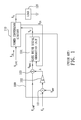
- FIG. 1 illustrates a power conversion application, in which a prior art controller 100 having a power factor correction mechanism is used to control a power conversion circuit 110 such that the waveform of an input current I IN of the power conversion circuit 110 is analog to that of a line voltage V LINE , and the average of the input current I IN is regulated to result in a DC output voltage V O for a load 120.
- the controller includes a combiner 101, an amplifier 102, a multiplier 103, and a gate drive signal generation unit 104.
- the combiner 101 is used to generate an error signal by subtracting V O with a reference voltage V REF .
- the amplifier 102 having a high DC gain and a cutoff frequency below 120 H z , is used to amplify the error signal with a negative gain to generate an amplitude adjusting signal A.
- the multiplier 103 is used to multiply the line voltage V LINE with the amplitude adjusting signal A to generate a reference current signal S REFC .
- the gate drive signal generation unit 104 is used to generate a gate drive signal V G to control the switching of the power conversion circuit 110, wherein the duty of the gate drive signal V G is determined according to a voltage comparison of the reference current signal S REFC and a current sensing signal S CS , which represents the input current I IN .
- the current sensing signal S CS When in operation, the current sensing signal S CS will follow the reference current signal S REFC , and the negative feedback mechanism will force V O to approach V REF . As such, if the line voltage V LINE is changed to a higher/lower level, the amplitude of the reference current signal S REFC will be adjusted by the amplitude adjusting signal A to a smaller/larger value to result in a lower/higher level of the current sensing signal S CS so as to regulate V O at V REF .
- the reference current signal S REFC of which the waveform is analog to that of the line voltage V LINE , and of which the amplitude is equal to the product of the amplitude adjusting signal A and the amplitude of the line voltage V LINE , is the key signal for achieving power factor correction and output voltage regulation at the same time.
- the present invention proposes a power conversion controller having a novel power factor correction mechanism for power conversion applications.
- the major objective of the present invention is to propose a power conversion controller having a novel power factor correction mechanism for a power conversion circuit, which can be of buck type, buck-boost type, or boost type etc..
- a power conversion controller having a novel power factor correction mechanism including:
- FIG 2 illustrates a power conversion application, in which a controller 200 having a novel power factor correction mechanism according to a preferred embodiment of the present invention is used to control a power conversion circuit 230, such that the waveform of an input current I IN is analog to a line voltage V LINE , and the average of the output current I O is regulated according to a constant level to supply a load 240 with a corresponding output voltage V O .
- the controller 200 includes a reference current signal generation module 210-having a normalization unit 211 and a reference current generation unit 212-and a gate drive signal generation unit 220.
- the normalization unit 211 is used to generate a normalized signal V NORM according to the line voltage V LINE by multiplying the line voltage V LINE with a normalizing gain S G , wherein the normalizing gain S G is proportional to the reciprocal of the amplitude of the line voltage V LINE .
- the gate drive signal generation unit 220 is used to generate a gate drive signal V G , wherein the duty of the gate drive signal V G is determined by a voltage comparison of the reference current signal S REFC and a current sensing signal S CS .
- the reference current signal S REFC can be used as a peak reference current to determine the peak value of the current sensing signal S CD , or used as an average reference current to determine the average value of the current sensing signal S CS .
- the reference current signal S REFC so designed can render a constant average output current and an excellent power factor in the meantime for this type of application. The principle is elaborated as follows:
- V LINE expressed as V A sin ⁇ , 0° ⁇ 180° for a cycle of the full-wave rectified line voltage V LINE , and the switching frequency of V G is much higher than that of V LINE
- S REFC V NORM ⁇ S G as a peak reference current
- the reference current signal S REFC so designed can render a constant average output current and an excellent power factor in the meantime for this type of application. The principle is elaborated as follows:
- V LINE expressed as V A sin ⁇ , 0° ⁇ 180° for a cycle of the full-wave rectified line voltage V LINE , and the switching frequency of V G is much higher than that of V LINE
- S REFC V NORM as a peak reference current
- the input current is in phase with the line voltage V LINE , and the average output current over the cycle of the full-wave rectified line voltage V LINE is independent of the amplitude of V LINE .
- the buffer 412 can be replaced with another equivalent circuit-a feedthrough connection for example.
- the reference current signal S REFC so designed can render a constant average output current and an excellent power factor in the meantime for this type of application, and what is more, since the average output current will be independent of the output voltage, the design is especially suitable for a LED lighting application, of which the output voltage can vary a lot due to the spec variation of LEDs.
- the principle is elaborated as follows:
- V LINE expressed as V A sin ⁇ , 0° ⁇ 180° for a cycle of the full-wave rectified line voltage V LINE , and the switching frequency of V G is much higher than that of V LINE
- S REFC V NORM ⁇ V NORM as a peak reference current for boundary current mode operation
- I IN,avg represents the average of the input current I IN
- t ON is the active period of V G
- t OFF is the inactive period of V G
- K is a constant
- the average output current I O,avg can be expressed as I
- the input current is in phase with the line voltage V LINE , and the average output current over the cycle of the full-wave rectified line voltage V LINE is independent of the amplitude of V LINE and Vo.
- the reference current signal S REFC so designed can render a constant average output current and an excellent power factor in the meantime for this type of application, and what is more, since the average output current will be independent of the output voltage, the design is especially suitable for a LED lighting application, of which the output voltage can vary a lot due to the spec variation of LEDs.
- the principle is elaborated as follows:
- V LINE V A sin ⁇ , 0° ⁇ 180° for a cycle of the full-wave rectified line voltage V LINE , and the switching frequency of V G is much higher than that of V LINE
- S REFC V NORM ⁇ (V NORM + V O ⁇ S G ) as a peak reference current for boundary current mode operation
- V O V O (Ksin ⁇ ) 2 /2
- I IN,avg represents the average of the input current I IN , and K is a constant
- the reference current signal S REFC so designed can render a constant average output current and an excellent power factor in the meantime for this type of application, and what is more, since the average output current will be independent of the output voltage, the design is especially suitable for a LED lighting application, of which the output voltage can vary a lot due to the spec variation of LEDs.
- the principle is elaborated as follows:
- V LINE expressed as V A sin ⁇ , 0° ⁇ 180° for a cycle of the full-wave rectified line voltage V LINE , and the switching frequency of V G is much higher than that of V LINE
- S REFC V NORM ⁇ (V O S G ) as a peak reference current for boundary current mode operation
- V O V O (Ksin ⁇ ) 2
- I IN,avg represents the average of the input current I IN , and K is a constant
- the power conversion controller of the present invention having a normalization unit for processing a line voltage, a novel power factor correction mechanism for power converters of buck type, buck-boost type, boost type, fly-back type, etc. is proposed, and the large error amplifier needed in prior art is eliminated. Therefore, the present invention does improve the prior art controllers and is worthy of being granted a patent.
- the present invention herein enhances the performance than the conventional structure and further complies with the patent application requirements and is submitted to the Patent and Trademark Office for review and granting of the commensurate patent rights.
Abstract
Description
- The present invention relates to a power conversion controller, and more particularly to a power conversion controller capable of providing power factor correction for power conversion applications requiring load current regulation.
-
FIG. 1 illustrates a power conversion application, in which aprior art controller 100 having a power factor correction mechanism is used to control apower conversion circuit 110 such that the waveform of an input current IIN of thepower conversion circuit 110 is analog to that of a line voltage VLINE, and the average of the input current IIN is regulated to result in a DC output voltage VO for aload 120. As can be seen inFIG. 1 , the controller includes acombiner 101, anamplifier 102, amultiplier 103, and a gate drivesignal generation unit 104. - The
combiner 101 is used to generate an error signal by subtracting VO with a reference voltage VREF. Theamplifier 102, having a high DC gain and a cutoff frequency below 120 Hz, is used to amplify the error signal with a negative gain to generate an amplitude adjusting signal A. - The
multiplier 103 is used to multiply the line voltage VLINE with the amplitude adjusting signal A to generate a reference current signal SREFC. - The gate drive
signal generation unit 104 is used to generate a gate drive signal VG to control the switching of thepower conversion circuit 110, wherein the duty of the gate drive signal VG is determined according to a voltage comparison of the reference current signal SREFC and a current sensing signal SCS, which represents the input current IIN. - When in operation, the current sensing signal SCS will follow the reference current signal SREFC, and the negative feedback mechanism will force VO to approach VREF. As such, if the line voltage VLINE is changed to a higher/lower level, the amplitude of the reference current signal SREFC will be adjusted by the amplitude adjusting signal A to a smaller/larger value to result in a lower/higher level of the current sensing signal SCS so as to regulate VO at VREF. That is, the reference current signal SREFC, of which the waveform is analog to that of the line voltage VLINE, and of which the amplitude is equal to the product of the amplitude adjusting signal A and the amplitude of the line voltage VLINE, is the key signal for achieving power factor correction and output voltage regulation at the same time.
- However, there is a major disadvantage in this architecture-the
amplifier 102 occupies a large area due to the required high gain and low cut-off frequency. - In view of this problem, the present invention proposes a power conversion controller having a novel power factor correction mechanism for power conversion applications.
- The major objective of the present invention is to propose a power conversion controller having a novel power factor correction mechanism for a power conversion circuit, which can be of buck type, buck-boost type, or boost type etc..
- To achieve the foregoing objective of the present invention, a power conversion controller having a novel power factor correction mechanism is proposed, the power conversion controller including:
- a normalization unit, used to generate a normalized signal according to a line voltage by multiplying the line voltage with a normalizing gain, wherein the normalizing gain is proportional to the reciprocal of the amplitude of the line voltage;
- a reference current generation unit, coupled to the normalization unit to generate a reference current signal by performing an arithmetic operation, wherein the arithmetic operation involves the normalized signal; and
- a gate drive signal generation unit, used to generate a gate drive signal, wherein the duty of the gate drive signal is determined by a voltage comparison of the reference current signal and a current sensing signal.
- To make it easier for our examiner to understand the objective of the invention, its structure, innovative features, and performance, we use preferred embodiments together with the accompanying drawings for the detailed description of the invention.
-
-
FIG 1 illustrates a power conversion application, in which a prior art controller having a power factor correction mechanism is used to control a power conversion circuit such that the waveform of an input current is analog to that of a line voltage, and the average of the input current is regulated to result in a DC output voltage for a load. -
FIG 2 illustrates a power conversion application, in which a controller having a novel power factor correction mechanism according to a preferred embodiment of the present invention is used to control a power conversion circuit, such that the waveform of an input current is analog to a line voltage, and the average of the output current is regulated according to a constant level. -
FIG 3 illustrates the block diagram of a reference current signal generation module inFIG 2 according to a preferred embodiment of the present invention. -
FIG 4 illustrates the block diagram of a reference current signal generation module inFIG 2 according to another preferred embodiment of the present invention. -
FIG 5 illustrates the block diagram of a reference current signal generation module inFIG 2 according to still another preferred embodiment of the present invention. -
FIG 6 illustrates the block diagram of a reference current signal generation module inFIG 2 according to still another preferred embodiment of the present invention. -
FIG 7 illustrates the block diagram of a reference current signal generation module inFIG 2 according to still another preferred embodiment of the present invention. - The present invention will be described in more detail hereinafter with reference to the accompanying drawings that show the preferred embodiment of the invention.
- Please refer to
FIG 2 , which illustrates a power conversion application, in which acontroller 200 having a novel power factor correction mechanism according to a preferred embodiment of the present invention is used to control apower conversion circuit 230, such that the waveform of an input current IIN is analog to a line voltage VLINE, and the average of the output current IO is regulated according to a constant level to supply aload 240 with a corresponding output voltage VO. As can be seen inFIG 2 , thecontroller 200 includes a reference current signal generation module 210-having anormalization unit 211 and a reference current generation unit 212-and a gate drivesignal generation unit 220. - The
normalization unit 211 is used to generate a normalized signal VNORM according to the line voltage VLINE by multiplying the line voltage VLINE with a normalizing gain SG, wherein the normalizing gain SG is proportional to the reciprocal of the amplitude of the line voltage VLINE. Thenormalization unit 211 can utilize, for example but not limited to, an auto gain control mechanism to implement the equation: YNORM = VLINE × SG, wherein SG is derived through an adjusting process such that the amplitude of VNORM is constant irrespective of different amplitudes of VLINE. - The reference
current generation unit 212 is coupled to thenormalization unit 211 to generate a reference current signal SREFC by performing an arithmetic operation, wherein the arithmetic operation, which involves the normalized signal VNORM, can be one selected from the group consisting of SREFC = VNORM × SG, SREFC = VNORM, SREFC = VNORM × VNORM, SREFC = VNORM × (VNORM + VO × SG), and SREFC = VNORM × (VO × SG). - The gate drive
signal generation unit 220 is used to generate a gate drive signal VG, wherein the duty of the gate drive signal VG is determined by a voltage comparison of the reference current signal SREFC and a current sensing signal SCS. - For different types of power converter in different operation modes, different forms of the arithmetic operation involving the normalized signal VNORM can be used, and, during the voltage comparison process, the reference current signal SREFC can be used as a peak reference current to determine the peak value of the current sensing signal SCD, or used as an average reference current to determine the average value of the current sensing signal SCS.
- For example, if the power conversion application is a boundary current mode boost convertor, then the reference current
signal generation module 210 can be implemented with the circuit block illustrated inFIG 3 , which includes anormalization unit 211 and amultiplier 312 to realize the equation SREFC = VNORM × SG. The reference current signal SREFC so designed can render a constant average output current and an excellent power factor in the meantime for this type of application. The principle is elaborated as follows: - With VLINE expressed as VAsinθ, 0°<θ<180° for a cycle of the full-wave rectified line voltage VLINE, and the switching frequency of VG is much higher than that of VLINE, by employing SREFC = VNORM × SG as a peak reference current, during one switching cycle, the input power can be expressed as VLINE × IIN,avg = VLINE × SREFC/2 = VLINE × VNORM × SG/2 = VNORM × VNORM/2 = (Ksinθ)2/2, wherein IIN,avg represents the average of the input current IIN, SG = K/VA, and K is a constant; and the average output current IO,avg can be expressed as IO,avg = (SREFC/2) × tOFF/(tON + tOFF) = (SREFc/2) × VLINE/VO = (VNORM × SG/2) × VLINE/VO = (VNORM)2/2VO = (Ksinθ)2/2VO, wherein tON is the active period of VG and tOFF is the inactive period of VG. As such, the input current IIN is in phase with the line voltage VLINE, and the average output current over the cycle of the full-wave rectified line voltage VLINE is independent of the amplitude of VLINE.
- Further, if the power conversion application is a discontinuous current mode fixed frequency flyback convertor, then the reference current
signal generation module 210 can be implemented with the circuit block illustrated inFIG 4 , which includes anormalization unit 211 and abuffer 412 to realize the equation SREFC = VNORM. The reference current signal SREFC so designed can render a constant average output current and an excellent power factor in the meantime for this type of application. The principle is elaborated as follows: - With VLINE expressed as VAsinθ, 0°<θ<180° for a cycle of the full-wave rectified line voltage VLINE, and the switching frequency of VG is much higher than that of VLINE, by employing SREFC = VNORM as a peak reference current, during one switching cycle, the input power can be expressed as VLINE × IIN,avg = L(SREFC)2/2T = L(VNORM)2/2T = L(Ksinθ)2/2T, wherein IIN,avg represents the average of the input current IIN, L is the inductance of an inductor, K is a constant and T is the switching cycle period; and the average output current IO,avg can be expressed as IO,avg = PIN/VO = L(Ksinθ)2/2TVO, wherein PIN is the input power. As such, the input current is in phase with the line voltage VLINE, and the average output current over the cycle of the full-wave rectified line voltage VLINE is independent of the amplitude of VLINE. It is to be noted that the
buffer 412 can be replaced with another equivalent circuit-a feedthrough connection for example. - Still further, if the power conversion application is a buck convertor or a forward convertor considered as a primary side equivalent circuit, then the reference current
signal generation module 210 can be implemented with the circuit block illustrated inFIG 5 , which includes anormalization unit 211 and amultiplier 512 to realize the equation SREFC = VNORM × VNORM The reference current signal SREFC so designed can render a constant average output current and an excellent power factor in the meantime for this type of application, and what is more, since the average output current will be independent of the output voltage, the design is especially suitable for a LED lighting application, of which the output voltage can vary a lot due to the spec variation of LEDs. The principle is elaborated as follows: - With VLINE expressed as VAsinθ, 0°<θ<180° for a cycle of the full-wave rectified line voltage VLINE, and the switching frequency of VG is much higher than that of VLINE, by employing SREFC = VNORM × VNORM as a peak reference current for boundary current mode operation, during one switching cycle, the input power can be expressed as VLINE × IIN,avg = VLINE × ((SREFC/2) × tOFF/(tON + TOFF)) = VLINE × ((SREFC/2) × VO/VLINE) = (VNORM )2 × VO/2 = VO(Ksinθ)2/2, wherein IIN,avg represents the average of the input current IIN, tON is the active period of VG, tOFF is the inactive period of VG, and K is a constant; and the average output current IO,avg can be expressed as IO,avg = SREFC/2 = (VNORM)2/2 = (Ksinθ)2/2.
- As for continuous current mode, by employing SREFC = VNORM × VNORM as an average reference current, during one switching cycle, the input power can be expressed as VLINE × IIN,avg = VLINE × (SREFC × VO/VLINE) = (VNORM)2 × VO = VO(Ksinθ)2, wherein IIN,avg represents the average of the input current IIN, and K is a constant; and the average output current IO,avg can be expressed as IO,avg = SREFC = (VNORM)2 = (Ksinθ)2. As such, the input current is in phase with the line voltage VLINE, and the average output current over the cycle of the full-wave rectified line voltage VLINE is independent of the amplitude of VLINE and Vo.
- Still further, if the power conversion application is a buck-boost convertor or a flyback convertor considered as a primary side equivalent circuit, then the reference current
signal generation module 210 can be implemented with the circuit block illustrated inFIG 6 , which includes anormalization unit 211, avariable gain amplifier 612a, acombiner 612b, and amultiplier 612c to realize the equation SREFC = VNORM × (VNORM + VO × SG). The reference current signal SREFC so designed can render a constant average output current and an excellent power factor in the meantime for this type of application, and what is more, since the average output current will be independent of the output voltage, the design is especially suitable for a LED lighting application, of which the output voltage can vary a lot due to the spec variation of LEDs. The principle is elaborated as follows: - With VLINE expressed as VAsinθ, 0°<θ<180° for a cycle of the full-wave rectified line voltage VLINE, and the switching frequency of VG is much higher than that of VLINE, by employing SREFC = VNORM × (VNORM + VO × SG) as a peak reference current for boundary current mode operation, during one switching cycle, the input power can be expressed as VLINE × IIN,avg = VLINE × ((SREFC/2) × VO/(VLINE+VO)) = (VNORM)2/2 × VO = VO(Ksinθ)2/2, wherein IIN,avg represents the average of the input current IIN, and K is a constant; and the average output current IO,avg can be expressed as IO,avg = (SREFC/2) × tOFF/(tON + tOFF)) = (SREFC/2) × VLINE/(VO+VLINE) = VNORM × (VNORM + VO × SG) × VLINE/(VO+VLINE)/2 = (VNORM)2/2 = (Ksinθ)2/2, wherein tON is the active period of VG and tOFF is the inactive period of VG.
- As for continuous current mode, by employing SREFC = VNORM × (VNORM + VO × SG) as an average reference current, during one switching cycle, the input power can be expressed as VLINE × IIN,avg = VLINE × (SREFC × VO/(VLINE+VO)) = (VNORM)2 × VO = VO(Ksinθ)2, wherein IIN,avg represents the average of the input current IIN, and K is a constant; and the average output current IO,avg can be expressed as IO,avg = SREFC × tOFF/(tON + tOFF)) = SREFC × VLINE/(VO+VLINE) = VNORM × (VNORM + VO × SG) × VLINE/(VO+VLINE) = (VNORM)2 = (Ksinθ)2, wherein tON is the active period of VG and tOFF is the inactive period of VG. As such, the input current is in phase with the line voltage VLINE, and the average output current over the cycle of the full-wave rectified line voltage VLINE is independent of the amplitude of VLINE and VO.
- Still further, if the power conversion application is a boost convertor, then the reference current
signal generation module 210 can be implemented with the circuit block illustrated inFIG 7 , which includes anormalization unit 211, avariable gain amplifier 712a, and amultiplier 712c to realize the equation SREFC = VNORM × (VO × SG). The reference current signal SREFC so designed can render a constant average output current and an excellent power factor in the meantime for this type of application, and what is more, since the average output current will be independent of the output voltage, the design is especially suitable for a LED lighting application, of which the output voltage can vary a lot due to the spec variation of LEDs. The principle is elaborated as follows: - With VLINE expressed as VAsinθ, 0°<θ<180° for a cycle of the full-wave rectified line voltage VLINE, and the switching frequency of VG is much higher than that of VLINE, by employing SREFC = VNORM × (VO SG) as a peak reference current for boundary current mode operation, during one switching cycle, the input power can be expressed as VLINE IIN,avg = VLINE SREFC = VLINE VNORM (VO × SG) = (VNORM)2 × VO = VO(Ksinθ)2, wherein IIN,avg represents the average of the input current IIN, and K is a constant; and the average output current IO,avg can be expressed as IO,avg = (SREFC/2) × tOFF/(tON + TOFF) = (SREFC/2) × VLINE / VO = VNORM × (VO × SG) × VLINE / Vo /2 = (VNORM)2/2 = (Ksinθ)2/2, wherein tON is the active period of VG and tOFF is the inactive period of VG.
- As for continuous current mode, by employing SREFC = VNORM × (VO × SG) as an average reference current, during one switching cycle, the input power can be expressed as VLINE × IIN,avg = VLINE × SREFC = VLINE × VNORM × (VO × SG) = (VNORM)2 × VO = VO(Ksinθ)2, wherein IIN,avg represents the average of the input current IIN, and K is a constant; and the average output current IO,avg can be expressed as IO,avg = SREFC × tOFF/(tON + tOFF) = SREFC × VLINE / VO = VNORM × (VO × SG) × VLINE / VO = (VNORM)2 = (Ksinθ)2, wherein tON is the active period of VG and tOFF is the inactive period of VG. As such, the input current is in phase with the line voltage VLINE, and the average output current over the cycle of the full-wave rectified line voltage VLINE is independent of the amplitude of VLINE and VO.
- As can be seen from the specification above, by using the power conversion controller of the present invention having a normalization unit for processing a line voltage, a novel power factor correction mechanism for power converters of buck type, buck-boost type, boost type, fly-back type, etc. is proposed, and the large error amplifier needed in prior art is eliminated. Therefore, the present invention does improve the prior art controllers and is worthy of being granted a patent.
- While the invention has been described by way of example and in terms of a preferred embodiment, it is to be understood that the invention is not limited thereto. To the contrary, it is intended to cover various modifications and similar arrangements and procedures, and the scope of the appended claims therefore should be accorded the broadest interpretation so as to encompass all such modifications and similar arrangements and procedures.
- In summation of the above description, the present invention herein enhances the performance than the conventional structure and further complies with the patent application requirements and is submitted to the Patent and Trademark Office for review and granting of the commensurate patent rights.
Claims (10)
- A power conversion controller having a novel power factor correction mechanism, comprising:a normalization unit (211), using an auto gain control mechanism to generate a normalized signal and a normalizing gain according to a line voltage, wherein said normalized signal is equal to the product of said line voltage and said normalizing gain, and said normalizing gain is proportional to the reciprocal of the amplitude of said line voltage;a reference current generation unit (212), coupled to said normalization unit (211) to generate a reference current signal by performing an arithmetic operation, wherein said arithmetic operation involves said normalized signal; anda gate drive signal generation unit (220), used to generate a gate drive signal, wherein the duty of said gate drive signal is determined by a voltage comparison of said reference current signal and a current sensing signal.
- The power conversion controller having a novel power factor correction mechanism as claim 1, wherein said reference current generation unit (212) comprises a multiplier (312) to implement said arithmetic operation as: SREFC = VNORM × SG, wherein SREFC represents said reference current signal, VNORM represents said normalized signal, and SG represents said normalizing gain.
- The power conversion controller having a novel power factor correction mechanism as claim 1, wherein said reference current generation unit (212) comprises a buffer (412) to implement said arithmetic operation as: SREFC = VNORM, wherein SREFC represents said reference current signal, and VNORM represents said normalized signal.
- The power conversion controller having a novel power factor correction mechanism as claim 1, wherein said reference current generation unit (212) comprises a multiplier (512) to implement said arithmetic operation as: SREFC = VNORM × VNORM, wherein SREFC represents said reference current signal, and VNORM represents said normalized signal.
- The power conversion controller having a novel power factor correction mechanism as claim 1, wherein said reference current generation unit (212) comprises a variable gain amplifier (612a), a combiner (612b), and a multiplier (612c) to implement said arithmetic operation as: SREFC = VNORM × (VNORM + VO × SG), wherein SREFC represents said reference current signal, VNORM represents said normalized signal, VO represents an output voltage, and SG represents said normalizing gain.
- The power conversion controller having a novel power factor correction mechanism as claim 1, wherein said reference current generation unit (212) comprises a variable gain amplifier (712a), and a multiplier (712c) to implement said arithmetic operation as: SREFC = VNORM × (VO × SG), wherein SREFC represents said reference current signal, VNORM represents said normalized signal, VO represents an output voltage, and SG represents said normalizing gain.
- A power conversion controller having a novel power factor correction mechanism, comprising:a normalization unit (211), used to generate a normalized signal according to a line voltage by multiplying said line voltage with a normalizing gain, wherein said normalizing gain is proportional to the reciprocal of the amplitude of said line voltage;a reference current generation unit (212), coupled to said normalization unit to generate a reference current signal by performing an arithmetic operation, wherein said arithmetic operation involves said normalized signal; anda gate drive signal generation unit (220), used to generate a gate drive signal, wherein the duty of said gate drive signal is determined by a voltage comparison of said reference current signal and a current sensing signal.
- The power conversion controller having a novel power factor correction mechanism as claim 7, wherein said reference current generation unit (212) is used to implement said arithmetic operation according to one selected from the group consisting of SREFC = VNORM × SG, SREFC VNORM, SREFC = VNORM × VNORM, SREFC = VNORM × (VNORM + VO × SG), and SREFC = VNORM × (VO × SG), wherein SREFC represents said reference current signal, VNORM represents said normalized signal, VO represents an output voltage, and SG represents said normalizing gain.
- The power conversion controller having a novel power factor correction mechanism as claim 8, wherein said reference current signal is used as a peak reference current in said gate drive signal generation unit (220).
- The power conversion controller having a novel power factor correction mechanism as claim 8, wherein said reference current signal is used as an average reference current in said gate drive signal generation unit (220).
Applications Claiming Priority (1)
| Application Number | Priority Date | Filing Date | Title |
|---|---|---|---|
| US12/953,219 US8541990B2 (en) | 2010-11-23 | 2010-11-23 | Power conversion controller having a novel power factor correction mechanism using line voltage normalization |
Publications (2)
| Publication Number | Publication Date |
|---|---|
| EP2469979A2 true EP2469979A2 (en) | 2012-06-27 |
| EP2469979A3 EP2469979A3 (en) | 2012-07-04 |
Family
ID=45463196
Family Applications (1)
| Application Number | Title | Priority Date | Filing Date |
|---|---|---|---|
| EP11175556A Withdrawn EP2469979A3 (en) | 2010-11-23 | 2011-07-27 | Power conversion controller having a novel power factor correction mechanism |
Country Status (3)
| Country | Link |
|---|---|
| US (1) | US8541990B2 (en) |
| EP (1) | EP2469979A3 (en) |
| JP (1) | JP2012115123A (en) |
Families Citing this family (12)
| Publication number | Priority date | Publication date | Assignee | Title |
|---|---|---|---|---|
| TWI396956B (en) * | 2009-09-18 | 2013-05-21 | Richtek Technology Corp | Average current regulator and driver circuit thereof and method for regulating average current |
| US8390357B2 (en) * | 2011-05-27 | 2013-03-05 | Immense Advance Technology Corp. | Fixed dead time PFC controller |
| TWI492504B (en) * | 2012-03-24 | 2015-07-11 | Richtek Technology Corp | Power supply circuit with pfc function, and automatic gain control circuit therefor and control method thereof |
| US10159117B2 (en) | 2012-05-18 | 2018-12-18 | Neturen Co., Ltd. | Induction heating system, induction heating method, output monitoring apparatus, output monitoring method, and induction heating apparatus |
| US9130457B2 (en) * | 2012-10-24 | 2015-09-08 | Qualcomm Incorporated | Control logic for switches coupled to an inductor |
| US9548794B2 (en) | 2013-05-03 | 2017-01-17 | Cooper Technologies Company | Power factor correction for constant current input with power line communication |
| US9000736B2 (en) | 2013-05-03 | 2015-04-07 | Cooper Technologies Company | Power factor correction algorithm for arbitrary input waveform |
| US9190901B2 (en) | 2013-05-03 | 2015-11-17 | Cooper Technologies Company | Bridgeless boost power factor correction circuit for constant current input |
| US9214855B2 (en) | 2013-05-03 | 2015-12-15 | Cooper Technologies Company | Active power factor correction circuit for a constant current power converter |
| TWI480716B (en) * | 2013-11-27 | 2015-04-11 | Voltronic Power Technology Corp | Control circuit having total harmonic distortion of current and method thereof |
| US9214854B2 (en) | 2014-02-18 | 2015-12-15 | Voltronics Power Technology Corp. | Total harmonic current distortion control circuit and method thereof |
| CN114070015B (en) * | 2020-08-05 | 2023-09-15 | 上海南芯半导体科技股份有限公司 | Driving control method and driving system of power device |
Family Cites Families (12)
| Publication number | Priority date | Publication date | Assignee | Title |
|---|---|---|---|---|
| JP2001314085A (en) * | 2000-04-28 | 2001-11-09 | Matsushita Electric Ind Co Ltd | Power supply apparatus, inverter apparatus and air conditioner |
| US7102340B1 (en) * | 2003-01-21 | 2006-09-05 | Microsemi Corporation | Dual-mode PFM boost converter |
| US7202641B2 (en) * | 2003-12-12 | 2007-04-10 | Philips Lumileds Lighting Company, Llc | DC-to-DC converter |
| US7266001B1 (en) * | 2004-03-19 | 2007-09-04 | Marvell International Ltd. | Method and apparatus for controlling power factor correction |
| US7733678B1 (en) * | 2004-03-19 | 2010-06-08 | Marvell International Ltd. | Power factor correction boost converter with continuous, discontinuous, or critical mode selection |
| US7812576B2 (en) * | 2004-09-24 | 2010-10-12 | Marvell World Trade Ltd. | Power factor control systems and methods |
| US7205749B2 (en) * | 2005-02-28 | 2007-04-17 | Texas Instruments Incorporated | Power line communication using power factor correction circuits |
| WO2007069239A2 (en) * | 2005-12-12 | 2007-06-21 | Poweroffer | Apparatus, method and system for control of ac/ac conversion |
| US8237372B2 (en) * | 2006-12-04 | 2012-08-07 | Nxp B.V. | Electronic device for driving light emitting diodes |
| US7554473B2 (en) * | 2007-05-02 | 2009-06-30 | Cirrus Logic, Inc. | Control system using a nonlinear delta-sigma modulator with nonlinear process modeling |
| JP5170096B2 (en) * | 2007-07-09 | 2013-03-27 | 株式会社村田製作所 | PFC converter |
| CN101237190A (en) * | 2008-01-25 | 2008-08-06 | 魏其萃 | High-precision average output current control scheme for critical interrupted and continuous current mode of power current converter |
-
2010
- 2010-11-23 US US12/953,219 patent/US8541990B2/en not_active Expired - Fee Related
-
2011
- 2011-07-13 JP JP2011154612A patent/JP2012115123A/en active Pending
- 2011-07-27 EP EP11175556A patent/EP2469979A3/en not_active Withdrawn
Non-Patent Citations (1)
| Title |
|---|
| None |
Also Published As
| Publication number | Publication date |
|---|---|
| US8541990B2 (en) | 2013-09-24 |
| US20120126759A1 (en) | 2012-05-24 |
| JP2012115123A (en) | 2012-06-14 |
| EP2469979A3 (en) | 2012-07-04 |
Similar Documents
| Publication | Publication Date | Title |
|---|---|---|
| EP2469979A2 (en) | Power conversion controller having a novel power factor correction mechanism | |
| TWI645277B (en) | Envelope-tracking power supply modulator | |
| US9621028B2 (en) | Digitally controlled PFC converter with multiple discontinuous modes | |
| US8823346B2 (en) | System and method of feed forward for boost converters with improved power factor and reduced energy storage | |
| US7808299B2 (en) | Switching power converter with reduced switching losses | |
| US9680375B2 (en) | Switching mode power supply with adaptively randomized spread spectrum | |
| EP2466740B1 (en) | Circuit of high efficient buck-boost switching regulator and control method thereof | |
| US20060043942A1 (en) | Power converter apparatus and methods using output current feedforward control | |
| TWI523385B (en) | Multi-mode controlled power converter | |
| US8723494B2 (en) | Switching power converter current limit reference circuit | |
| TWI484739B (en) | Active power factor correction circuit and related pfc controller | |
| US20110157921A1 (en) | Multi-output dc-to-dc conversion apparatus with voltage-stabilizing function | |
| JP2013197098A (en) | Light driving apparatus and method of the same | |
| JP5930700B2 (en) | Switching power supply device and control method thereof | |
| US20140327421A1 (en) | Switching regulator and method for controlling the switching regulator | |
| TW202027389A (en) | Switched mode power supply with pfc burst mode control | |
| US8787045B1 (en) | Control method for inhibiting harmonic distortion of input current | |
| US9847709B2 (en) | Switched-mode power supply device | |
| US9774245B1 (en) | PFC switching power conversion circuit providing low total harmonic distortion | |
| US8659271B2 (en) | Fixed-on-time controller utilizing an adaptive saw signal for discontinuous mode PFC power conversion | |
| US9515575B2 (en) | Power conversion apparatus and power conversion method | |
| US20210257905A1 (en) | Power factor correction circuit with burst setting and method of operating the same | |
| US8390357B2 (en) | Fixed dead time PFC controller | |
| TWI473406B (en) | Digitalized feed-forward power factor corrected converter with wide-range output voltage and method thereof | |
| US20140092644A1 (en) | Switching power supply device and method for circuit design of the switching power supply device |
Legal Events
| Date | Code | Title | Description |
|---|---|---|---|
| PUAL | Search report despatched |
Free format text: ORIGINAL CODE: 0009013 |
|
| AK | Designated contracting states |
Kind code of ref document: A2 Designated state(s): AL AT BE BG CH CY CZ DE DK EE ES FI FR GB GR HR HU IE IS IT LI LT LU LV MC MK MT NL NO PL PT RO RS SE SI SK SM TR |
|
| AX | Request for extension of the european patent |
Extension state: BA ME |
|
| PUAI | Public reference made under article 153(3) epc to a published international application that has entered the european phase |
Free format text: ORIGINAL CODE: 0009012 |
|
| AK | Designated contracting states |
Kind code of ref document: A3 Designated state(s): AL AT BE BG CH CY CZ DE DK EE ES FI FR GB GR HR HU IE IS IT LI LT LU LV MC MK MT NL NO PL PT RO RS SE SI SK SM TR |
|
| AX | Request for extension of the european patent |
Extension state: BA ME |
|
| RIC1 | Information provided on ipc code assigned before grant |
Ipc: H02M 3/157 20060101ALI20120531BHEP Ipc: H05B 33/08 20060101AFI20120531BHEP |
|
| 17P | Request for examination filed |
Effective date: 20121221 |
|
| STAA | Information on the status of an ep patent application or granted ep patent |
Free format text: STATUS: THE APPLICATION HAS BEEN WITHDRAWN |
|
| 18W | Application withdrawn |
Effective date: 20140516 |