EP2469700A1 - Electrostatic induction power generator - Google Patents
Electrostatic induction power generator Download PDFInfo
- Publication number
- EP2469700A1 EP2469700A1 EP10809833A EP10809833A EP2469700A1 EP 2469700 A1 EP2469700 A1 EP 2469700A1 EP 10809833 A EP10809833 A EP 10809833A EP 10809833 A EP10809833 A EP 10809833A EP 2469700 A1 EP2469700 A1 EP 2469700A1
- Authority
- EP
- European Patent Office
- Prior art keywords
- electrode
- substrate
- electret
- electrostatic capacitance
- electrostatic
- Prior art date
- Legal status (The legal status is an assumption and is not a legal conclusion. Google has not performed a legal analysis and makes no representation as to the accuracy of the status listed.)
- Granted
Links
Images





Classifications
-
- H—ELECTRICITY
- H02—GENERATION; CONVERSION OR DISTRIBUTION OF ELECTRIC POWER
- H02N—ELECTRIC MACHINES NOT OTHERWISE PROVIDED FOR
- H02N1/00—Electrostatic generators or motors using a solid moving electrostatic charge carrier
-
- H—ELECTRICITY
- H02—GENERATION; CONVERSION OR DISTRIBUTION OF ELECTRIC POWER
- H02N—ELECTRIC MACHINES NOT OTHERWISE PROVIDED FOR
- H02N1/00—Electrostatic generators or motors using a solid moving electrostatic charge carrier
- H02N1/06—Influence generators
- H02N1/08—Influence generators with conductive charge carrier, i.e. capacitor machines
Definitions
- the present invention relates to an electrostatic induction generator.
- an electrostatic induction generator in which a pair of substrates that can move relatively while remaining opposed to each other is provided, plural electrets are arrayed in one of the substrates, and plural sets of pairs of electrodes are arrayed on the other substrate.
- an electrostatic capacitance between one of the pair of electrodes and the electret and an electrostatic capacitance between the other electrode and the electret change by the relative movement of the pair of substrates respectively, whereby the change amount is output as an electric power.
- ⁇ is surface charge density in the pair of electrodes
- n is (amplitude of the pair of substrates ⁇ a pitch between the electrets)
- A is a maximum area in which the electret and the electrode overlap each other
- ⁇ e is specific permittivity of the electret
- d is a thickness of the electret
- ⁇ 0 is vacuum permittivity
- g is a gap between the pair of substrates.
- the output power can be increased on the equation 1 by decreasing the pitch between the electrets.
- An object of the present invention is to provide an electrostatic induction generator that achieves the improvement of the power generation efficiency.
- the inventors were able to find the generation region of the parasitic capacitance that causes the degradation of the power generation efficiency. From the viewpoint of a technical common sense, it has been considered that the parasitic capacitance generated in a certain region of the pair of electrodes causes the degradation of the power generation efficiency. On the other hand, it has been considered that the parasitic capacitance generated between the electrodes, which are provided on the same substrate, is ignorable because each of the electrodes is constructed by a thin film. However, the inventors found that the parasitic capacitance generated between the electrodes causes the degradation of the power generation efficiency.
- the present invention provides an electrostatic induction generator including: a first substrate and a second substrate, which can move relatively while remaining opposed to each other; an electret that is provided in the first substrate; and a first electrode and a second electrode, which are provided on a surface side opposed to the electret in the second substrate, wherein a positional relationship between the electret and the first electrode and a positional relationship between the electret and the second electrode change in association with a change of relative positions between the first substrate and the second substrate, whereby an electrostatic capacitance between the electret and the first electrode and an electrostatic capacitance between the electret and the second electrode change to output an electric power, and a structure that decreases the electrostatic capacitance between the first electrode and the second electrode (a specific structure that decreases the electrostatic capacitance between the first electrode and the second electrode, not only providing the first electrode and the second electrode on the substrate) is provided between the first electrode and the second electrode.
- the structure that decreases the electrostatic capacitance between the first electrode and the second electrode is provided between the electrodes, so that the parasitic capacitance generated between the electrodes can be decreased. Accordingly, the power generation efficiency can be improved.
- the structure that decreases the electrostatic capacitance may be a structure that is provided between the first electrode and the second electrode to decrease the permittivity between the first electrode and the second electrode.
- the following configurations may be adopted as the structure that decreases the permittivity between the electrodes.
- the configuration in which permittivity between the first electrode and the second electrode is decreased by making a through-hole in a portion between the first electrode and the second electrode in the second substrate may be adopted.
- the configuration in which the permittivity between the first electrode and the second electrode is decreased by providing a recess in a portion between the first electrode and the second electrode in the second substrate may be adopted.
- the configuration in which the permittivity between the first electrode and the second electrode is decreased by providing a layer made of a material having specific permittivity lower than that of the second substrate in a portion between the second substrate and the first electrode, and between the second substrate and the second electrode may be adopted.
- the two configurations described above may be combined with this configuration.
- a surface side opposed to the first substrate is covered with an insulating film. Therefore, a discharge from the electret can be prevented.
- the power generation efficiency can be improved.
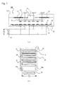
- FIG. 1(a) is a schematic sectional view illustrating a whole of the electrostatic induction generator of the embodiment.
- Fig. 1(b) is a schematic configuration diagram illustrating a configuration of a second substrate described below. In Fig. 1(b) , the second substrate is viewed in plan configuration.
- An electrostatic induction generator 100 of the embodiment includes a chassis 110, a first substrate 10, and a second substrate 20, and the first substrate 10 and the second substrate 20 are provided in the chassis 110.
- the first substrate 10 is retained by a retention member 11.
- the retention member 11 is supported by a pair of springs 12, in which one end thereof is fixed onto an inner wall surface side of the chassis 110 while the other end is fixed to the retention member 11. Therefore, the retention member 11 can move (oscillate) in a horizontal direction of Fig. 1(a) , and the first substrate 10 also moves (oscillates) in conjunction with the retention member 11.
- the first substrate 10 and the second substrate 20 are disposed opposite to each other.
- the first substrate 10 and the second substrate 20 are configured to move while remaining opposed to each other. That is, the first substrate 10 and the second substrate 20 are configured to be able to move relatively while remaining opposed to each other.
- the first substrate 10 is configured to be able to move.
- the second substrate 20 may be configured to be able to move, or both the first substrate 10 and the second substrate 20 may be configured to be able to move.
- plural electrets 13 each of which is formed on a conductor and plural grounded guard electrodes 14 are alternately arrayed on a surface side opposed to the second substrate 20.
- the electret 13 is configured to semipermanently retain a negative charge.
- first electrodes 21 1 and second electrodes 22 plural pairs of electrodes (first electrodes 21 1 and second electrodes 22) are arrayed on a surface side opposed to the first substrate 10.
- the first electrodes 21 included in the pairs are electrically connected to one another, and the second electrodes 22 are also electrically connected to one another.
- the first electrodes 21 and the second electrodes 22 are electrically connected by use of a comb-shaped electrode, respectively (see Fig. 1(b) ).
- a load 30 to which an electric power obtained by power generation is electrically connected through a first electrode pad 21 a electrically connected to the first electrodes 21 and a second electrode pad 21 b electrically connected to the second electrodes 22.
- an electrostatic capacitance decreasing structure 23 that decreases an electrostatic capacitance between the first electrode 21 and the second electrode 22 is provided between the first electrode 21 and the second electrode 22.
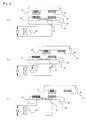
- FIG. 2(a) illustrates a state in which the whole surface of the electret 13 is opposed to the whole surface of the first electrode 21 while the electret 13 is not opposed to the second electrode 22 at all.
- Fig. 2(b) illustrates a state in which the electret 13 is not opposed to the first electrode 21 at all while the electret 13 is partially opposed to the second electrode 22.
- Fig. 2(c) illustrates a state in which the whole surface of the electret 13 is opposed to the whole surface of the second electrode 22 while the electret 13 is not opposed to the first electrode 21 at all.
- the electrostatic capacitance between the electret 13 and the first electrode 21 is maximized in the state of Fig. 2(a) .
- the electrostatic capacitance between the electret 13 and the second electrode 22 is maximized in the state of Fig. 2(c) .
- the electrostatic capacitance between the electret 13 and the first electrode 21 1 and the electrostatic capacitance between the electret 13 and the second electrode 22 change respectively by the movement of the first substrate 10.
- Fig. 2(b) illustrates the state in the middle of a transition from the state of Fig. 2(a) to the state of Fig. 2(c) .
- electrostatic capacitance between the electret 13 and the first electrode 21 is decreased, and the electrostatic capacitance between the electret 13 and the second electrode 22 is increased. Because the first electrode 21 and the second electrode 22 are electrically connected through the load 30, a positive charge moves from the first electrode 21 toward the second electrode 22. Therefore, the electric power is generated.
- Fig. 3 is a graph illustrating a variation in output voltage V to an elapsed time t when the state of Fig. 2(a) and the state of Fig. 2(c) vary alternately with a constant period (the first substrate 10 oscillates (moves reciprocally) with a constant period).
- t1 corresponds to the time in the state of Fig. 2(a)
- t2 corresponds to the time in the state of Fig. 2(c) .
- the output voltage draws a curve in which a center of a high voltage and a low voltage becomes 0 (V) as illustrated in Fig. 3 .
- the center of the high voltage and the low voltage can be set to 0 (V) by providing the guard electrode 14.
- a potential at the second electrode 22 becomes 0 (V) by a Kirchhoff law in the state in which the electret 13 is opposed to the first electrode 21 while the grounded guard electrode 14 is opposed to the second electrode 22.
- the first electrode 21 is opposed to the guard electrode 14 (not illustrated in Fig. 2(c) ) and the potential at the first electrode 21 becomes 0 (V). Accordingly, the curve of the output voltage can be obtained as illustrated in Fig. 3 , and the output voltage can stably be obtained.
- a parasitic capacitance will be described with reference to Figs. 4 and 5 .
- the output power is expected to be enhanced when a pitch between the electrets is decreased while n is increased.
- the output voltage cannot be enhanced according to the equation 1. This is attributed to the fact that the parasitic capacitance is generated in one of regions of the generator. However, it has been unclear which region, in which the parasitic capacitance is generated, degrades power generation efficiency. As a result of discussions and trials, the inventors found that the parasitic capacitance generated between the first electrode 21 and the second electrode 22 degrades the power generation efficiency.
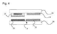
- Fig. 4 illustrates a state in which the electret 13 is opposed to the first electrode 21 while the guard electrode 14 is opposed to the second electrode 22 in a conventional structure that does not include the electrostatic capacitance decreasing structure 23.
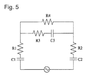
- Fig. 5 is an equivalent circuit diagram of the electrostatic induction generator in the state of Fig. 4 . ln Fig. 5 , C1 and R1 correspond to an electrostatic capacitance and an electric resistance between the electret 13 and the first electrode 21, respectively, C2 and R2 correspond to an electrostatic capacitance and an electric resistance between the electret 13 and the second electrode 22, respectively, C3 and R3 correspond to an electrostatic capacitance and an electric resistance between the first electrode 21 and the second electrode 22, respectively, and R4 corresponds to an electric resistance of the load 30. The output power is consumed by the electric resistance R4 of the load 30.
- the electric power consumed by the electric resistance R4 is decreased with increasing electrostatic capacitance C3. That is, the power generation efficiency is degraded.
- the electrostatic induction generator has an electrode size (as illustrated in Fig. 1(b) , vertical and horizontal lengths of a portion corresponding to a domain Z where the plural electrodes are disposed) of 20 ⁇ 20 mm, a line width of the electrode (in Fig.
- the electrostatic capacitance (corresponding to C1) between the electret 13 and the first electrode 21 was 20 pF
- the electrostatic capacitance (corresponding to C2) between the electret 13 and the second electrode 22 was 15.8 pF
- the electrostatic capacitance (corresponding to C3) between the first electrode 21 and the second electrode 22 was 75 pF.
- the electrostatic capacitance decreasing structure 23 is provided between the first electrode 21 and the second electrode 22. Therefore, the electrostatic capacitance C3 that becomes the parasitic capacitance causing the degradation of the power generation efficiency can be decreased to improve the power generation efficiency.
- the electrostatic capacitance C3 is expressed by C3 ⁇ ⁇ ⁇ L ⁇ log (D/a).
- ⁇ permittivity between the first electrode 21 and the second electrode 22
- D is a gap between the first electrode 21 and the second electrode 22
- a is a half (1/2) of a thickness of the first electrode 21 and the second electrode 22
- L is a total length of a domain where the first electrode 21 is opposed to the second electrode 22 (in the case of the configuration of Fig. 1 (b) , L corresponds to the total length of a portion indicated by an alternate long and short dash line).
- the permittivity ⁇ between the first electrode 21 and the second electrode 22 is decreased with decreasing specific permittivity of a body that exists in a domain connecting the first electrode 21 and the second electrode 22. In the case that a space made of air or vacuum exists in the domain connecting the first electrode 21 and the second electrode 22, the permittivity ⁇ is decreased with increasing space.
- a through-hole 23a is made in a portion between the first electrode 21 and the second electrode 22 of the second substrate 20. Therefore, a large space (a domain made of air or vacuum) is formed between the first electrode 21 and the second electrode 22. Accordingly, the permittivity between the electrodes can be decreased.
- the electrostatic capacitance between the first electrode 21 and the second electrode 22 can be decreased to about 1/4 by making the through-hole 23a.
- a metallic electrode (corresponding to the first electrode 21 and the second electrode 22) is formed on the second substrate 20.
- the metallic electrode is formed on the film.
- the metallic electrode is directly formed on the glass surface.
- a material such as aluminum, gold, and copper which has high conductivity is used as the material for the metallic electrode, a metallic film is formed on the substrate by evaporation, sputtering, and the like, and a pattern is formed by photolithography. Then the through-hole 23a is made.
- the through-hole 23a can be made by wet etching with KOH or TMAH, dry etching, and the like.
- the through-hole 23a can be made by dry etching, blasting, laser machining, wet etching with HF, and the like.
- a recess is formed in the portion between the first electrode 21 and the second electrode 22 of the second substrate 20.
- Fig. 7(a) illustrates the case that a recess 23b is constructed by a groove having a rectangular shape in section
- Fig. 7(b) illustrates the case that a recess 23c is constructed by a groove having a triangular shape in section.
- the sectional shape of the recess is not limited to the shapes of Figs. 7(a) and 7(b) .
- a surface constituting the recess is not limited to the flat surface, but the surface may have a curved portion.
- the space (the domain made of air or vacuum) is formed between the first electrode 21 and the second electrode 22.
- the large space is formed between the first electrode 21 and the second electrode 22.
- the small space is formed between the first electrode 21 and the second electrode 22 compared with the case of the first examples.
- the large space can be formed between the first electrode 21 and the second electrode 22. Accordingly, the permittivity between the electrodes can be decreased.
- the method for producing the electrostatic capacitance decreasing structure in the second substrate 20 is similar to that of the first example.
- the recess is formed to an extent that the recess does not reach the through-hole, so that the electrostatic capacitance decreasing structure can be produced at lower cost compared with the case of the first example.
- the glass substrate having the specific permittivity of 4 to 4.7 is used as the material for the second substrate 20
- the electrostatic capacitance between the first electrode 21 and the second electrode 22 can be decreased to about 1/2 by providing the recesses 23b or 23c. The reason the permittivity can be decreased by providing the recess will be described in detail by taking the configuration of Fig. 7(b) as an example. As illustrated in Fig.
- C' is an electrostatic capacitance when the recess 23c is provided, and it is assumed that D1 and D2 are distances on the left and right of an apex in the substantially triangular recess 23c, respectively.
- layers 23d made of a material having the specific permittivity lower than that of the second substrate 20 are provided between the second substrate 20 and the first electrode 21 and between the second substrate 20 and the second electrode 22, respectively.
- the recess (the groove having the rectangular shape in section) is formed between the first electrode 21 and the second electrode 22 in the second substrate 20. Accordingly, the large space can be formed between the first electrode 21 and the second electrode 22. Further, the layers 23d made of the material having the specific permittivity lower than that of the second substrate 20 are interposed between the second substrate 20 and the first electrode 21 and between the second substrate 20 and the second electrode 22, respectively. Accordingly, the permittivity between the first electrode 21 and the second electrode 22 can be decreased.
- a method for producing the electrostatic capacitance decreasing structure in the second substrate 20 having the above configuration will briefly be described.
- a layer (film) made of a material (such as a fluorine resin, parylene, and an interlayer insulating material) having the low specific permittivity is formed on the second substrate 20 by CDV or application (such as spin coating and dipping).
- the metallic electrode is formed on the layer.
- the recess is formed by dry etching (such as 02 ashing), blasting, thermal transfer with a metallic mold, and the like.
- the groove having the rectangular shape in section is illustrated as the recess.
- the groove having the triangular shape in section may be used as the recess.
- the sectional shape of the recess is not limited to the shapes of Fig. 8 .
- the surface constituting the recess is not limited to the flat surface, but the surface may have the curved portion.
- the electrostatic capacitance decreasing structure in the second substrate 20 can be produced at lower cost compared with the case of the first example.
- the glass substrate having the specific permittivity of 4 to 4.7 is used as the material for the second substrate 20
- the electrostatic capacitance between the first electrode 21 and the second electrode 22 can be decreased to about 1/2 by interposing the layer 23d.
- the electrostatic capacitance of each portion was measured similarly to the case of Fig. 4 .
- the electrostatic induction generator has the electrode size (as illustrated in Fig. 1(b) , vertical and horizontal lengths of a portion corresponding to a domain Z where the plural electrodes are disposed) of 20 ⁇ 20 mm, the line width of the electrode (in Fig.
- the electrostatic capacitance (corresponding to C1) between the electret 13 and the first electrode 21 was 20 pF
- the electrostatic capacitance (corresponding to C2) between the electret 13 and the second electrode 22 was 13.4 pF
- the electrostatic capacitance (corresponding to C3) between the first electrode 21 and the second electrode 22 was 41 pF.
- an electrostatic capacitance decreasing structure according to a fourth example of the present invention will be described with reference to Fig. 9 .
- layers 23d1 made of a material having the specific permittivity lower than that of the second substrate 20 are provided between the second substrate 20 and the first electrode 21 and between the second substrate 20 and the second electrode 22, respectively, and a recess 23b1 is provided in the second substrate 20. That is, the characteristic configuration of the second example and the characteristic configuration of the third example are combined in the fourth example.
- the electrostatic capacitance between the first electrode 21 and the second electrode 22 can further be decreased compared with the second and third examples.
- FIG. 10 An electrostatic capacitance decreasing structure according to a fifth example of the present invention will be described with reference to Fig. 10 .
- a surface side opposed to the first substrate 10 is covered with an insulating film 40.
- Fig. 10(a) illustrates the case that the structure of the first example is adopted as the electrostatic capacitance decreasing structure of the fifth example
- Fig. 10(b) illustrates the case that the structure of the second example is adopted as the electrostatic capacitance decreasing structure of the fifth example.
- the structures of the third and fourth examples may also be adopted.
- the surface side opposed to the first substrate 10 is covered with the insulating film 40, so that a discharge from the electret 13 can be prevented.
Landscapes
- Engineering & Computer Science (AREA)
- Power Engineering (AREA)
- Micromachines (AREA)
Abstract
Description
- The present invention relates to an electrostatic induction generator.
- Conventionally there is well known an electrostatic induction generator, in which a pair of substrates that can move relatively while remaining opposed to each other is provided, plural electrets are arrayed in one of the substrates, and plural sets of pairs of electrodes are arrayed on the other substrate. In the electrostatic induction generator, an electrostatic capacitance between one of the pair of electrodes and the electret and an electrostatic capacitance between the other electrode and the electret change by the relative movement of the pair of substrates respectively, whereby the change amount is output as an electric power.
- Assuming that the pair of electrodes is made of the same material and has the same configuration and that the pair of substrates moves relatively (moves reciprocally) so as to oscillate at a constant frequency f, Boland, et al. say that a maximum output power Pmax is expressed by Pmax = σ2nA2πf ÷ [(
ε e ε 0/d) × ((ε e g/d) + 1)]. Hereinafter, the above mathematical formula is referred to as an equation 1. - At this point, σ is surface charge density in the pair of electrodes, n is (amplitude of the pair of substrates ÷ a pitch between the electrets), A is a maximum area in which the electret and the electrode overlap each other, εe is specific permittivity of the electret, d is a thickness of the electret, ε0 is vacuum permittivity, and g is a gap between the pair of substrates.
- According to the equation 1, it is necessary to increase n in order to enhance the output power. That is, it is necessary to increase the amplitude of the pair of substrates or to decrease the pitch between the electrets, However, when miniaturization of the electrostatic induction generator is demanded, there is a limitation to the increase in amplitude of the pair of substrates. In such cases, the output power can be increased on the equation 1 by decreasing the pitch between the electrets.
- However, actually it is demonstrated that the output power cannot be increased as calculated even if the pitch between the electrets is decreased. According to a report, this is attributed to the fact that a parasitic capacitance generated in one of regions of the electrostatic induction generator degrades power generation efficiency (see Non-Patent Document 1). However, it has been unclear which region, in which the parasitic capacitance is generated, degrades the power generation efficiency.
- Related technologies are disclosed in Patent Documents 1 to 3.
-
- Patent Document 1: Japanese Unexamined Patent Publication No.
2008-161036 - Patent Document 2: Japanese Unexamined Patent Publication No.
2009-77614 - Patent Document 3: Japanese Unexamined Patent Publication No.
2008-252847 -
- Non-Patent Document 1: T. Tsutsumino, Y. Suzuki, N. Kasagi, K. Kashiwagi, and Y. Morizawa, "Micro Seismic Electret Generator for Energy Harvesting", The Sixth International Workshop and Nanotechnology for Power Generation and Energy Conversion Applications; Power MEMS 2006, November 29 - December 1, 2006, Berkeley, U. S. A.
- An object of the present invention is to provide an electrostatic induction generator that achieves the improvement of the power generation efficiency.
- As a result of discussions and trials, the inventors were able to find the generation region of the parasitic capacitance that causes the degradation of the power generation efficiency. From the viewpoint of a technical common sense, it has been considered that the parasitic capacitance generated in a certain region of the pair of electrodes causes the degradation of the power generation efficiency. On the other hand, it has been considered that the parasitic capacitance generated between the electrodes, which are provided on the same substrate, is ignorable because each of the electrodes is constructed by a thin film. However, the inventors found that the parasitic capacitance generated between the electrodes causes the degradation of the power generation efficiency.
- Therefore, a structure that decreases the electrostatic capacitance between the electrodes is adopted in the present invention.
- More specifically, the present invention provides an electrostatic induction generator including: a first substrate and a second substrate, which can move relatively while remaining opposed to each other; an electret that is provided in the first substrate; and a first electrode and a second electrode, which are provided on a surface side opposed to the electret in the second substrate, wherein a positional relationship between the electret and the first electrode and a positional relationship between the electret and the second electrode change in association with a change of relative positions between the first substrate and the second substrate, whereby an electrostatic capacitance between the electret and the first electrode and an electrostatic capacitance between the electret and the second electrode change to output an electric power, and a structure that decreases the electrostatic capacitance between the first electrode and the second electrode (a specific structure that decreases the electrostatic capacitance between the first electrode and the second electrode, not only providing the first electrode and the second electrode on the substrate) is provided between the first electrode and the second electrode.
- According to the present invention, the structure that decreases the electrostatic capacitance between the first electrode and the second electrode is provided between the electrodes, so that the parasitic capacitance generated between the electrodes can be decreased. Accordingly, the power generation efficiency can be improved.
- In order to decrease the electrostatic capacitance between the electrodes, it is conceivable that the distance between the electrodes is lengthened, or it is conceivable that the permittivity between the electrodes is decreased. However, when miniaturization of the electrostatic induction generator is achieved, there is a limitation to the increase in length between the electrodes.
- Therefore, the structure that decreases the electrostatic capacitance may be a structure that is provided between the first electrode and the second electrode to decrease the permittivity between the first electrode and the second electrode.
- The following configurations may be adopted as the structure that decreases the permittivity between the electrodes.
- In other words, the configuration in which permittivity between the first electrode and the second electrode is decreased by making a through-hole in a portion between the first electrode and the second electrode in the second substrate may be adopted.
- The configuration in which the permittivity between the first electrode and the second electrode is decreased by providing a recess in a portion between the first electrode and the second electrode in the second substrate may be adopted.
- The configuration in which the permittivity between the first electrode and the second electrode is decreased by providing a layer made of a material having specific permittivity lower than that of the second substrate in a portion between the second substrate and the first electrode, and between the second substrate and the second electrode may be adopted. The two configurations described above may be combined with this configuration.
- Preferably, on a second substrate side, a surface side opposed to the first substrate is covered with an insulating film. Therefore, a discharge from the electret can be prevented.
- As described above, according to the present invention, the power generation efficiency can be improved.
-
-
Fig. 1 is a schematic configuration diagram of an electrostatic induction generator according to an embodiment of the present invention. -
Fig. 2 is a view illustrating a power generation principle of the electrostatic induction generator according to the embodiment of the present invention. -
Fig. 3 is a view illustrating an output voltage of the electrostatic induction generator according to the embodiment of the present invention. -
Fig. 4 is a view illustrating generation of a parasitic capacitance in the electrostatic induction generator. -
Fig. 5 is an equivalent circuit diagram when the parasitic capacitance is generated in the electrostatic induction generator. -
Fig. 6 is a schematic sectional view illustrating an electrostatic capacitance decreasing structure according to a first example of the present invention. -
Fig. 7 is a schematic sectional view illustrating an electrostatic capacitance decreasing structure according to a second example of the present invention. -
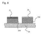
Fig. 8 is a schematic sectional view illustrating an electrostatic capacitance decreasing structure according to a third example of the present invention. -
Fig. 9 is a schematic sectional view illustrating an electrostatic capacitance decreasing structure according to a fourth example of the present invention. -
Fig. 10 is a schematic sectional view illustrating an electrostatic capacitance decreasing structure according to a fifth example of the present invention. - Hereinafter, best modes for carrying out the invention will be described with reference to the drawings. However, the present invention is not limited to sizes, materials, shapes, relative dispositions and the like of the components described in the following embodiment and examples.
- An entire configuration of an electrostatic induction generator according to an embodiment of the present invention will be described with reference to
Fig. 1. Fig. 1(a) is a schematic sectional view illustrating a whole of the electrostatic induction generator of the embodiment.Fig. 1(b) is a schematic configuration diagram illustrating a configuration of a second substrate described below. InFig. 1(b) , the second substrate is viewed in plan configuration. Anelectrostatic induction generator 100 of the embodiment includes achassis 110, afirst substrate 10, and asecond substrate 20, and thefirst substrate 10 and thesecond substrate 20 are provided in thechassis 110. - The
first substrate 10 is retained by aretention member 11. Theretention member 11 is supported by a pair ofsprings 12, in which one end thereof is fixed onto an inner wall surface side of thechassis 110 while the other end is fixed to theretention member 11. Therefore, theretention member 11 can move (oscillate) in a horizontal direction ofFig. 1(a) , and thefirst substrate 10 also moves (oscillates) in conjunction with theretention member 11. - The
first substrate 10 and thesecond substrate 20 are disposed opposite to each other. Thefirst substrate 10 and thesecond substrate 20 are configured to move while remaining opposed to each other. That is, thefirst substrate 10 and thesecond substrate 20 are configured to be able to move relatively while remaining opposed to each other. In the embodiment, thefirst substrate 10 is configured to be able to move. Alternatively, thesecond substrate 20 may be configured to be able to move, or both the first substrate 10 and thesecond substrate 20 may be configured to be able to move. - In the
first substrate 10,plural electrets 13 each of which is formed on a conductor and plural groundedguard electrodes 14 are alternately arrayed on a surface side opposed to thesecond substrate 20. In the embodiment, theelectret 13 is configured to semipermanently retain a negative charge. - In the
second substrate 20, plural pairs of electrodes (first electrodes 21 1 and second electrodes 22) are arrayed on a surface side opposed to thefirst substrate 10. Thefirst electrodes 21 included in the pairs are electrically connected to one another, and thesecond electrodes 22 are also electrically connected to one another. In the embodiment, thefirst electrodes 21 and thesecond electrodes 22 are electrically connected by use of a comb-shaped electrode, respectively (seeFig. 1(b) ). Aload 30 to which an electric power obtained by power generation is electrically connected through afirst electrode pad 21 a electrically connected to thefirst electrodes 21 and a second electrode pad 21 b electrically connected to thesecond electrodes 22. - In the
electrostatic induction generator 100 of the embodiment, a structure (hereinafter referred to as an electrostatic capacitance decreasing structure 23) that decreases an electrostatic capacitance between thefirst electrode 21 and thesecond electrode 22 is provided between thefirst electrode 21 and thesecond electrode 22. - A power generation principle of the electrostatic induction generator of the embodiment will be described with reference to
Figs. 2 and3 . - A relative positional relationship between the
first substrate 10 and thesecond substrate 20 changes by the movement of thefirst substrate 10. Therefore, a positional relationship between theelectret 13 and thefirst electrode 21 and a positional relationship between theelectret 13 and thesecond electrode 22 also change.Fig. 2(a) illustrates a state in which the whole surface of theelectret 13 is opposed to the whole surface of thefirst electrode 21 while theelectret 13 is not opposed to thesecond electrode 22 at all.Fig. 2(b) illustrates a state in which theelectret 13 is not opposed to thefirst electrode 21 at all while theelectret 13 is partially opposed to thesecond electrode 22.Fig. 2(c) illustrates a state in which the whole surface of theelectret 13 is opposed to the whole surface of thesecond electrode 22 while theelectret 13 is not opposed to thefirst electrode 21 at all. - The electrostatic capacitance between the
electret 13 and thefirst electrode 21 is maximized in the state ofFig. 2(a) . At this point, there is also an electrostatic capacitance between theelectret 13 and thesecond electrode 22. The electrostatic capacitance between theelectret 13 and thesecond electrode 22 is maximized in the state ofFig. 2(c) . At this point, there is also an electrostatic capacitance between theelectret 13 and thefirst electrode 21. The electrostatic capacitance between theelectret 13 and thefirst electrode 21 1 and the electrostatic capacitance between theelectret 13 and thesecond electrode 22 change respectively by the movement of thefirst substrate 10. -
Fig. 2(b) illustrates the state in the middle of a transition from the state ofFig. 2(a) to the state ofFig. 2(c) . During a procedure of the transition, electrostatic capacitance between theelectret 13 and thefirst electrode 21 is decreased, and the electrostatic capacitance between theelectret 13 and thesecond electrode 22 is increased. Because thefirst electrode 21 and thesecond electrode 22 are electrically connected through theload 30, a positive charge moves from thefirst electrode 21 toward thesecond electrode 22. Therefore, the electric power is generated. -
Fig. 3 is a graph illustrating a variation in output voltage V to an elapsed time t when the state ofFig. 2(a) and the state ofFig. 2(c) vary alternately with a constant period (thefirst substrate 10 oscillates (moves reciprocally) with a constant period). InFig. 3 , t1 corresponds to the time in the state ofFig. 2(a) , and t2 corresponds to the time in the state ofFig. 2(c) . - At this point, in order to stably obtain the output voltage, desirably the output voltage draws a curve in which a center of a high voltage and a low voltage becomes 0 (V) as illustrated in
Fig. 3 . !n the embodiment, in the output voltage, the center of the high voltage and the low voltage can be set to 0 (V) by providing theguard electrode 14. For example, as illustrated inFig. 2(a) , a potential at thesecond electrode 22 becomes 0 (V) by a Kirchhoff law in the state in which theelectret 13 is opposed to thefirst electrode 21 while the groundedguard electrode 14 is opposed to thesecond electrode 22. In the state ofFig. 2(c) , thefirst electrode 21 is opposed to the guard electrode 14 (not illustrated inFig. 2(c) ) and the potential at thefirst electrode 21 becomes 0 (V). Accordingly, the curve of the output voltage can be obtained as illustrated inFig. 3 , and the output voltage can stably be obtained. - A parasitic capacitance will be described with reference to
Figs. 4 and5 . As described above in the background art, according to the equation 1, the output power is expected to be enhanced when a pitch between the electrets is decreased while n is increased. However, actually the output voltage cannot be enhanced according to the equation 1. This is attributed to the fact that the parasitic capacitance is generated in one of regions of the generator. However, it has been unclear which region, in which the parasitic capacitance is generated, degrades power generation efficiency. As a result of discussions and trials, the inventors found that the parasitic capacitance generated between thefirst electrode 21 and thesecond electrode 22 degrades the power generation efficiency. - In other words, from the viewpoint of a technical common sense, in the electrostatic induction generator, it has been considered that the parasitic capacitance generated between the
first electrode 21 and thesecond electrode 22, which are provided on thesecond substrate 20, is ignorable because each of thefirst electrode 21 and thesecond electrode 22 is constructed by a thin film (for example, 1 µm or less). However, actually it is found that the parasitic capacitance generated between thefirst electrode 21 and thesecond electrode 22 degrades the power generation efficiency. -
Fig. 4 illustrates a state in which theelectret 13 is opposed to thefirst electrode 21 while theguard electrode 14 is opposed to thesecond electrode 22 in a conventional structure that does not include the electrostaticcapacitance decreasing structure 23. A charge distribution, in which the negative charges gather on a side surface on the side of thesecond electrode 22 in thefirst electrode 21 white the positive charges gather on a side surface on the side of thefirst electrode 21 in thesecond electrode 22, is assumed as illustrated by an arrow P inFig. 4 . -
Fig. 5 is an equivalent circuit diagram of the electrostatic induction generator in the state ofFig. 4 . lnFig. 5 , C1 and R1 correspond to an electrostatic capacitance and an electric resistance between theelectret 13 and thefirst electrode 21, respectively, C2 and R2 correspond to an electrostatic capacitance and an electric resistance between theelectret 13 and thesecond electrode 22, respectively, C3 and R3 correspond to an electrostatic capacitance and an electric resistance between thefirst electrode 21 and thesecond electrode 22, respectively, and R4 corresponds to an electric resistance of theload 30. The output power is consumed by the electric resistance R4 of theload 30. - As can be seen from the equivalent circuit diagram, the electric power consumed by the electric resistance R4 is decreased with increasing electrostatic capacitance C3. That is, the power generation efficiency is degraded.
- For example, in the electrostatic induction generator, the electrostatic capacitance of each portion was measured in the state of
Fig. 4 . The electrostatic induction generator has an electrode size (as illustrated inFig. 1(b) , vertical and horizontal lengths of a portion corresponding to a domain Z where the plural electrodes are disposed) of 20 × 20 mm, a line width of the electrode (inFig. 4 , a distance between thefirst electrode 21 and thesecond electrode 22 in a horizontal direction) of 300 µm, the gap between thefirst electrode 21 and thesecond electrode 22 of 20 µm, the film thicknesses of thefirst electrode 21 and thesecond electrode 22 of 0.4 µm, the gap between thefirst substrate 10 and thesecond substrate 20 of 100 µm, and the specific permittivity of thesecond substrate 20 of 4.7. - As a result of the measurement, the electrostatic capacitance (corresponding to C1) between the
electret 13 and thefirst electrode 21 was 20 pF, the electrostatic capacitance (corresponding to C2) between theelectret 13 and thesecond electrode 22 was 15.8 pF, and the electrostatic capacitance (corresponding to C3) between thefirst electrode 21 and thesecond electrode 22 was 75 pF. - Accordingly, ΔC = 20 pF - 15.8 pF = 4.2 pF and ΔC/20 pF = 0.21 were obtained, and it was found that only 21 % of the power generation amount calculated from the equation I was taken out as the electric power.
- In the embodiment, as described above, the electrostatic
capacitance decreasing structure 23 is provided between thefirst electrode 21 and thesecond electrode 22. Therefore, the electrostatic capacitance C3 that becomes the parasitic capacitance causing the degradation of the power generation efficiency can be decreased to improve the power generation efficiency. - At this point, the electrostatic capacitance C3 is expressed by C3≅ π εL ÷ log (D/a). Where ε is permittivity between the
first electrode 21 and thesecond electrode 22, D is a gap between thefirst electrode 21 and thesecond electrode 22, a is a half (1/2) of a thickness of thefirst electrode 21 and thesecond electrode 22, and L is a total length of a domain where thefirst electrode 21 is opposed to the second electrode 22 (in the case of the configuration ofFig. 1 (b) , L corresponds to the total length of a portion indicated by an alternate long and short dash line). - As can be seen from the above equation, in order to decrease the electrostatic capacitance C3 that becomes the parasitic capacitance, it is necessary to decrease the permittivity ε between the
first electrode 21 and thesecond electrode 22, or it is necessary to widen the gap between thefirst electrode 21 and thesecond electrode 22. Assuming that the amplitude of the pair of substrates is kept constant in the equation 1, because n is decreased, the latter means little. When the miniaturization of the electrostatic induction generator is demanded, there is a limitation to the increase of the gap between thefirst electrode 21 and thesecond electrode 22. Accordingly, the structure that decreases the permittivity ε between thefirst electrode 21 and thesecond electrode 22 is desirably adopted as the electrostaticcapacitance decreasing structure 23. - The permittivity ε between the
first electrode 21 and thesecond electrode 22 is decreased with decreasing specific permittivity of a body that exists in a domain connecting thefirst electrode 21 and thesecond electrode 22. In the case that a space made of air or vacuum exists in the domain connecting thefirst electrode 21 and thesecond electrode 22, the permittivity ε is decreased with increasing space. Some specific examples that implement the structure of the embodiment will be described below. - An electrostatic capacitance decreasing structure according to a first example of the present invention will be described with reference to
Fig. 6 . In the first example, a through-hole 23a is made in a portion between thefirst electrode 21 and thesecond electrode 22 of thesecond substrate 20. Therefore, a large space (a domain made of air or vacuum) is formed between thefirst electrode 21 and thesecond electrode 22. Accordingly, the permittivity between the electrodes can be decreased. For example, in the case that a glass substrate having the specific permittivity of 4 to 4.7 is used as the material for thesecond substrate 20, the electrostatic capacitance between thefirst electrode 21 and thesecond electrode 22 can be decreased to about 1/4 by making the through-hole 23a. - A method for producing the electrostatic capacitance decreasing structure in the
second substrate 20 having the above configuration will briefly be described. Firstly, a metallic electrode (corresponding to thefirst electrode 21 and the second electrode 22) is formed on thesecond substrate 20. In the case of a silicon substrate, after a film such as an oxide film which has a high insulating property is formed on a surface of the silicon substrate, the metallic electrode is formed on the film. In the case of the glass substrate, the metallic electrode is directly formed on the glass surface. A material such as aluminum, gold, and copper which has high conductivity is used as the material for the metallic electrode, a metallic film is formed on the substrate by evaporation, sputtering, and the like, and a pattern is formed by photolithography. Then the through-hole 23a is made. In the case of the silicon substrate, the through-hole 23a can be made by wet etching with KOH or TMAH, dry etching, and the like. In the case of the glass substrate, the through-hole 23a can be made by dry etching, blasting, laser machining, wet etching with HF, and the like. - An electrostatic capacitance decreasing structure according to a second example of the present invention will be described with reference to
Fig. 7 . In the second example, a recess is formed in the portion between thefirst electrode 21 and thesecond electrode 22 of thesecond substrate 20.Fig. 7(a) illustrates the case that arecess 23b is constructed by a groove having a rectangular shape in section, andFig. 7(b) illustrates the case that arecess 23c is constructed by a groove having a triangular shape in section. Although not illustrated, the sectional shape of the recess is not limited to the shapes ofFigs. 7(a) and 7(b) . For example, a surface constituting the recess is not limited to the flat surface, but the surface may have a curved portion. - In the second example, similarly to the first example, the space (the domain made of air or vacuum) is formed between the
first electrode 21 and thesecond electrode 22. In the case of the first example, the large space is formed between thefirst electrode 21 and thesecond electrode 22. On the other hand, in the second example, because the substrate exists in a position distant from the electrode, the small space is formed between thefirst electrode 21 and thesecond electrode 22 compared with the case of the first examples. However, compared with the case that the recess is not provided, the large space can be formed between thefirst electrode 21 and thesecond electrode 22. Accordingly, the permittivity between the electrodes can be decreased. The method for producing the electrostatic capacitance decreasing structure in thesecond substrate 20 is similar to that of the first example. - According to the second example, the recess is formed to an extent that the recess does not reach the through-hole, so that the electrostatic capacitance decreasing structure can be produced at lower cost compared with the case of the first example. In the case that the glass substrate having the specific permittivity of 4 to 4.7 is used as the material for the
second substrate 20, the electrostatic capacitance between thefirst electrode 21 and thesecond electrode 22 can be decreased to about 1/2 by providing therecesses Fig. 7(b) as an example. As illustrated inFig. 7(b) , it is assumed that D is the distance between thefirst electrode 21 and thesecond electrode 22, and it is assumed that D1 and D2 are widths of two tilt surfaces in therecess 23c, respectively. In the case that therecess 23c is eliminated, an electrostatic capacitance C approximately becomes C≅π s L ÷ log (D/a). Where ε is the permittivity between thefirst electrode 21 and thesecond electrode 22, L is the total length of the domain where thefirst electrode 21 is opposed to thesecond electrode 22, and a is a half (1/2) of the thickness of thefirst electrode 21 and thesecond electrode 22. On the other hand, it is assumed that C' is an electrostatic capacitance when therecess 23c is provided, and it is assumed that D1 and D2 are distances on the left and right of an apex in the substantiallytriangular recess 23c, respectively. The electrostatic capacitance C' approximately becomes C'≅ π ε L ÷ log ((D1 + D2) /a) = π ε' ÷ log (D/a). Therefore, it is found that the permittivity between thefirst electrode 21 and thesecond electrode 22 can be decreased. As described above, even if the positional relationship (distance) between thefirst electrode 21 and thesecond electrode 22 is not changed, the distance passing through the surface of the substrate is lengthened by providing the recess, which allows the permittivity between the electrodes can be decreased. - An electrostatic capacitance decreasing structure according to a third example of the present invention will be described with reference to
Fig. 8 . In the third example, layers 23d made of a material having the specific permittivity lower than that of thesecond substrate 20 are provided between thesecond substrate 20 and thefirst electrode 21 and between thesecond substrate 20 and thesecond electrode 22, respectively. - In the configuration of the third example, similarly to the second example, the recess (the groove having the rectangular shape in section) is formed between the
first electrode 21 and thesecond electrode 22 in thesecond substrate 20. Accordingly, the large space can be formed between thefirst electrode 21 and thesecond electrode 22. Further, thelayers 23d made of the material having the specific permittivity lower than that of thesecond substrate 20 are interposed between thesecond substrate 20 and thefirst electrode 21 and between thesecond substrate 20 and thesecond electrode 22, respectively. Accordingly, the permittivity between thefirst electrode 21 and thesecond electrode 22 can be decreased. - A method for producing the electrostatic capacitance decreasing structure in the
second substrate 20 having the above configuration will briefly be described. Firstly, a layer (film) made of a material (such as a fluorine resin, parylene, and an interlayer insulating material) having the low specific permittivity is formed on thesecond substrate 20 by CDV or application (such as spin coating and dipping). The metallic electrode is formed on the layer. Then the recess is formed by dry etching (such as 02 ashing), blasting, thermal transfer with a metallic mold, and the like. In the third example ofFig. 8 , the groove having the rectangular shape in section is illustrated as the recess. Alternatively, the groove having the triangular shape in section may be used as the recess. Although not illustrated, the sectional shape of the recess is not limited to the shapes ofFig. 8 . For example, the surface constituting the recess is not limited to the flat surface, but the surface may have the curved portion. - According to the third example, it is not necessary to make the through-hole in the substrate, so that the electrostatic capacitance decreasing structure in the
second substrate 20 can be produced at lower cost compared with the case of the first example. In the case that the glass substrate having the specific permittivity of 4 to 4.7 is used as the material for thesecond substrate 20, the electrostatic capacitance between thefirst electrode 21 and thesecond electrode 22 can be decreased to about 1/2 by interposing thelayer 23d. - For example, in the electrostatic induction generator, the electrostatic capacitance of each portion was measured similarly to the case of
Fig. 4 . The electrostatic induction generator has the electrode size (as illustrated inFig. 1(b) , vertical and horizontal lengths of a portion corresponding to a domain Z where the plural electrodes are disposed) of 20 × 20 mm, the line width of the electrode (inFig. 8 , the distance between thefirst electrode 21 and thesecond electrode 22 in the horizontal direction) of 300 µm, the gap between thefirst electrode 21 and thesecond electrode 22 of 20 µm, the film thicknesses of thefirst electrode 21 and thesecond electrode 22 of 0.4 µm, the gap between thefirst substrate 10 and thesecond substrate 20 of 100 µm, a thickness of thelayer 23d made of the fluorine resin of 15 µm, and the specific permittivity of thesecond substrate 20 of 4.7. - As a result of the measurement, the electrostatic capacitance (corresponding to C1) between the
electret 13 and thefirst electrode 21 was 20 pF, the electrostatic capacitance (corresponding to C2) between theelectret 13 and thesecond electrode 22 was 13.4 pF, and the electrostatic capacitance (corresponding to C3) between thefirst electrode 21 and thesecond electrode 22 was 41 pF. - Accordingly, ΔC = 20 pF - 13.4 pF = 6.6 pF and AC/20 pF = 0.33 were obtained, and it was found that 33% of the power generation amount calculated from the equation 1 was taken out as the electric power.
- An electrostatic capacitance decreasing structure according to a fourth example of the present invention will be described with reference to
Fig. 9 . In the fourth example, layers 23d1 made of a material having the specific permittivity lower than that of thesecond substrate 20 are provided between thesecond substrate 20 and thefirst electrode 21 and between thesecond substrate 20 and thesecond electrode 22, respectively, and a recess 23b1 is provided in thesecond substrate 20. That is, the characteristic configuration of the second example and the characteristic configuration of the third example are combined in the fourth example. According to the fourth example, the electrostatic capacitance between thefirst electrode 21 and thesecond electrode 22 can further be decreased compared with the second and third examples. - An electrostatic capacitance decreasing structure according to a fifth example of the present invention will be described with reference to
Fig. 10 . In the fifth example, on the side of thesecond substrate 20, a surface side opposed to thefirst substrate 10 is covered with an insulatingfilm 40.Fig. 10(a) illustrates the case that the structure of the first example is adopted as the electrostatic capacitance decreasing structure of the fifth example, andFig. 10(b) illustrates the case that the structure of the second example is adopted as the electrostatic capacitance decreasing structure of the fifth example. Although not illustrated, the structures of the third and fourth examples may also be adopted. - According to the fifth example, on the side of the
second substrate 20, the surface side opposed to thefirst substrate 10 is covered with the insulatingfilm 40, so that a discharge from theelectret 13 can be prevented. -
- 10
- first substrate
- 11
- retention member
- 12
- spring
- 13
- electret
- 14
- guard electrode
- 20
- second substrate
- 21
- first electrode
- 22
- second electrode
- 23
- electrostatic capacitance decreasing structure
- 23a
- through-hole
- 23b, 23b1, 23c
- recess
- 23d, 23d1
- layer
- 30
- load
- 40
- insulating film
- 100
- electrostatic induction generator
- 110
- chassis
Claims (6)
- An electrostatic induction generator comprising:a first substrate and a second substrate, which can move relatively while remaining opposed to each other;an electret that is provided in the first substrate; anda first electrode and a second electrode, which are provided on a surface side opposed to the electret in the second substrate, whereina positional relationship between the electret and the first electrode and a positional relationship between the electret and the second electrode change in association with a change of relative positions between the first substrate and the second substrate, whereby an electrostatic capacitance between the electret and the first electrode and an electrostatic capacitance between the electret and the second electrode change to output an electric power, anda structure that decreases the electrostatic capacitance between the first electrode and the second electrode is provided between the first electrode and the second electrode.
- The electrostatic induction generator according to claim 1, wherein
the structure that decreases the electrostatic capacitance is a structure that is provided between the first electrode and the second electrode to decrease permittivity between the first electrode and the second electrode. - The electrostatic induction generator according to claim 2, wherein
permittivity between the first electrode and the second electrode is decreased by making a through-hole in a portion between the first electrode and the second electrode in the second substrate. - The electrostatic induction generator according to claim 2, wherein
permittivity between the first electrode and the second electrode is decreased by providing a recess in a portion between the first electrode and the second electrode in the second substrate. - The electrostatic induction generator according to any one of claims 2, 3 and 4, wherein
permittivity between the first electrode and the second electrode is decreased by providing a layer made of a material having specific permittivity lower than that of the second substrate in a portion between the first electrode and the second electrode in the second substrate. - The electrostatic induction generator according to any one of claims 1 to 5, wherein,
on a second substrate side, a surface side opposed to the first substrate is covered with an insulating film.
Applications Claiming Priority (2)
| Application Number | Priority Date | Filing Date | Title |
|---|---|---|---|
| JP2009191993A JP5402395B2 (en) | 2009-08-21 | 2009-08-21 | Static induction generator |
| PCT/JP2010/062829 WO2011021488A1 (en) | 2009-08-21 | 2010-07-29 | Electrostatic induction power generator |
Publications (3)
| Publication Number | Publication Date |
|---|---|
| EP2469700A1 true EP2469700A1 (en) | 2012-06-27 |
| EP2469700A4 EP2469700A4 (en) | 2015-08-05 |
| EP2469700B1 EP2469700B1 (en) | 2018-11-07 |
Family
ID=43606943
Family Applications (1)
| Application Number | Title | Priority Date | Filing Date |
|---|---|---|---|
| EP10809833.6A Active EP2469700B1 (en) | 2009-08-21 | 2010-07-29 | Electrostatic induction power generator |
Country Status (6)
| Country | Link |
|---|---|
| US (1) | US8796902B2 (en) |
| EP (1) | EP2469700B1 (en) |
| JP (1) | JP5402395B2 (en) |
| KR (1) | KR101370786B1 (en) |
| CN (1) | CN102474203B (en) |
| WO (1) | WO2011021488A1 (en) |
Cited By (2)
| Publication number | Priority date | Publication date | Assignee | Title |
|---|---|---|---|---|
| EP2874304A4 (en) * | 2012-07-10 | 2016-06-01 | Omron Tateisi Electronics Co | DEVICE FOR GENERATING ELECTRICAL ENERGY OF VIBRATION |
| EP2876806A4 (en) * | 2012-07-19 | 2016-06-08 | Omron Tateisi Electronics Co | DEVICE FOR GENERATING ELECTRICITY FROM VIBRATIONS |
Families Citing this family (26)
| Publication number | Priority date | Publication date | Assignee | Title |
|---|---|---|---|---|
| JP5704426B2 (en) * | 2010-06-03 | 2015-04-22 | 国立大学法人東北大学 | Electrostatic energy converter |
| JP5304877B2 (en) * | 2011-03-09 | 2013-10-02 | カシオ計算機株式会社 | Power generation device and electronic device |
| WO2013132753A1 (en) | 2012-03-07 | 2013-09-12 | パナソニック株式会社 | Vibration power generator, vibration power generation device, and communication device and electronic device mounted with vibration power generation device |
| US20140070664A1 (en) * | 2012-03-26 | 2014-03-13 | Panasonic Corporation | Vibration power generator |
| JP5790584B2 (en) * | 2012-04-26 | 2015-10-07 | オムロン株式会社 | Vibration power generation element |
| JP6074939B2 (en) * | 2012-07-27 | 2017-02-08 | ソニー株式会社 | Generator |
| CN103368453B (en) * | 2013-03-12 | 2016-04-13 | 北京纳米能源与系统研究所 | A kind of sliding friction nano generator and electricity-generating method |
| CN103780124B (en) * | 2013-03-12 | 2015-12-09 | 北京纳米能源与系统研究所 | A sliding friction nanogenerator set |
| CN103780125B (en) * | 2013-03-13 | 2016-03-30 | 北京纳米能源与系统研究所 | A kind of jacket layer slidingtype friction nanometer power generator |
| WO2014148371A1 (en) | 2013-03-19 | 2014-09-25 | 国立大学法人東北大学 | Static induction-type vibration power generation device and method for producing same |
| KR101398708B1 (en) | 2014-01-09 | 2014-05-27 | 성균관대학교산학협력단 | Electrostatic energy harvester coupled with ferroelectric effect |
| KR101529814B1 (en) | 2014-01-09 | 2015-06-17 | 성균관대학교산학협력단 | Hybrid electric generating elements |
| WO2015146483A1 (en) * | 2014-03-26 | 2015-10-01 | シチズンホールディングス株式会社 | Electrostatic induction power generator |
| EP3133375B1 (en) * | 2014-04-18 | 2021-09-15 | Beijing Institute of Nanoenergy and Nanosystems | Sensor and power generator based on electrostatic induction, and sensing method and power generation method |
| CN104104263A (en) * | 2014-07-31 | 2014-10-15 | 向昭睿 | Inductive physical battery |
| KR101532887B1 (en) * | 2014-12-03 | 2015-07-02 | 성균관대학교산학협력단 | Triboelectric energy generator using control of dipole polarization direction and method of fabricating thereof |
| US20180164241A1 (en) | 2015-06-11 | 2018-06-14 | Dan Haronian | Micro-electromechanical device, system and method for energy harvesting and sensing |
| JP6682106B2 (en) * | 2015-10-02 | 2020-04-15 | 株式会社鷺宮製作所 | Vibration generator |
| EP3396843A4 (en) * | 2015-11-25 | 2019-10-09 | The University of Tokyo | ELECTROSTATIC INDUCTION GENERATION PRODUCTION ELEMENT |
| CN108886330A (en) * | 2016-03-17 | 2018-11-23 | 西铁城时计株式会社 | Electrostatic electromechanical transducer |
| JP6677125B2 (en) * | 2016-08-24 | 2020-04-08 | 株式会社デンソー | Semiconductor device |
| JP6335347B1 (en) | 2017-02-09 | 2018-05-30 | 株式会社トライフォース・マネジメント | Power generation element and power generation device |
| US10712879B2 (en) * | 2017-06-15 | 2020-07-14 | The Regents Of The University Of California | Touch capacitance transduced energy harvesting system |
| EP3683951A1 (en) | 2019-01-15 | 2020-07-22 | Enervibe Ltd. | Micro-electromechanical device for energy harvesting |
| WO2022201563A1 (en) * | 2021-03-25 | 2022-09-29 | ナミックス株式会社 | Laminate for wiring board |
| IT202200008738A1 (en) | 2022-05-02 | 2023-11-02 | Iinformatica Srl | Green system for the generation of clean energy from the wind and light radiation through trees, shrubs and plants and related clean energy generation method |
Family Cites Families (14)
| Publication number | Priority date | Publication date | Assignee | Title |
|---|---|---|---|---|
| JP4206904B2 (en) * | 2003-11-06 | 2009-01-14 | ソニー株式会社 | MEMS resonator |
| WO2005065385A2 (en) * | 2003-12-30 | 2005-07-21 | Fairchild Semiconductor Corporation | Power semiconductor devices and methods of manufacture |
| JP4935138B2 (en) | 2006-03-23 | 2012-05-23 | セイコーエプソン株式会社 | Circuit board, circuit board manufacturing method, electro-optical device, and electronic apparatus |
| JP5081833B2 (en) * | 2006-10-30 | 2012-11-28 | 三洋電機株式会社 | Electrostatic operation device |
| US8212450B2 (en) * | 2006-11-28 | 2012-07-03 | Sanyo Electric Co., Ltd. | Generator including an electret member |
| JP4338745B2 (en) | 2006-11-28 | 2009-10-07 | 三洋電機株式会社 | Electrostatic induction type conversion device |
| JP2008252847A (en) | 2007-03-30 | 2008-10-16 | Matsushita Electric Works Ltd | Electrostatic transducer |
| JP5028185B2 (en) * | 2007-08-28 | 2012-09-19 | 三洋電機株式会社 | Electrostatic generator |
| JP5487493B2 (en) | 2007-09-18 | 2014-05-07 | 国立大学法人東北大学 | Electret micro power generator |
| JP5033561B2 (en) * | 2007-09-26 | 2012-09-26 | 三洋電機株式会社 | Electrostatic generator |
| JP2009183015A (en) * | 2008-01-29 | 2009-08-13 | Sanyo Electric Co Ltd | Power generating apparatus |
| JP2009044949A (en) * | 2008-03-24 | 2009-02-26 | Sanyo Electric Co Ltd | Operation apparatus |
| JP5205193B2 (en) * | 2008-09-25 | 2013-06-05 | 三洋電機株式会社 | Static induction generator |
| WO2013132753A1 (en) * | 2012-03-07 | 2013-09-12 | パナソニック株式会社 | Vibration power generator, vibration power generation device, and communication device and electronic device mounted with vibration power generation device |
-
2009
- 2009-08-21 JP JP2009191993A patent/JP5402395B2/en not_active Expired - Fee Related
-
2010
- 2010-07-29 KR KR1020127000320A patent/KR101370786B1/en active Active
- 2010-07-29 WO PCT/JP2010/062829 patent/WO2011021488A1/en not_active Ceased
- 2010-07-29 US US13/386,907 patent/US8796902B2/en active Active
- 2010-07-29 CN CN201080031483.1A patent/CN102474203B/en active Active
- 2010-07-29 EP EP10809833.6A patent/EP2469700B1/en active Active
Non-Patent Citations (1)
| Title |
|---|
| See references of WO2011021488A1 * |
Cited By (3)
| Publication number | Priority date | Publication date | Assignee | Title |
|---|---|---|---|---|
| EP2874304A4 (en) * | 2012-07-10 | 2016-06-01 | Omron Tateisi Electronics Co | DEVICE FOR GENERATING ELECTRICAL ENERGY OF VIBRATION |
| EP2876806A4 (en) * | 2012-07-19 | 2016-06-08 | Omron Tateisi Electronics Co | DEVICE FOR GENERATING ELECTRICITY FROM VIBRATIONS |
| US10181805B2 (en) | 2012-07-19 | 2019-01-15 | Omron Corporation | Vibration power generator |
Also Published As
| Publication number | Publication date |
|---|---|
| JP5402395B2 (en) | 2014-01-29 |
| CN102474203B (en) | 2015-04-15 |
| EP2469700B1 (en) | 2018-11-07 |
| WO2011021488A1 (en) | 2011-02-24 |
| KR101370786B1 (en) | 2014-03-06 |
| JP2011045194A (en) | 2011-03-03 |
| CN102474203A (en) | 2012-05-23 |
| US20120181897A1 (en) | 2012-07-19 |
| KR20120027468A (en) | 2012-03-21 |
| EP2469700A4 (en) | 2015-08-05 |
| US8796902B2 (en) | 2014-08-05 |
Similar Documents
| Publication | Publication Date | Title |
|---|---|---|
| EP2469700B1 (en) | Electrostatic induction power generator | |
| JP5033561B2 (en) | Electrostatic generator | |
| JP5411871B2 (en) | Electret electrode, actuator using the same, vibration power generator, vibration power generation device, and communication device equipped with the vibration power generation device | |
| US8093784B2 (en) | Piezoelectric power generating element, and method of generating electric power using the piezoelectric power generating element | |
| US9496807B2 (en) | Electrostatic induction power generator | |
| US9455647B2 (en) | Electret element and vibration power generating device using the same | |
| KR101437246B1 (en) | Electrostatic induction power generator | |
| US11374507B2 (en) | Vibrational energy harvester device | |
| US20130241346A1 (en) | Device for converting mechanical energy into electrical energy | |
| WO2008026407A1 (en) | Electrostatic operation device | |
| JP5226907B1 (en) | Vibration power generator, vibration power generation device, and electrical equipment and communication device equipped with vibration power generation device | |
| JP6032006B2 (en) | Vibration power generator | |
| US9998035B2 (en) | Resonant energy harvester, aircraft component comprising the resonant energy harvester and an aircraft comprising the resonant energy harvester or the aircraft component | |
| US9804233B2 (en) | MEMS magnetic field sensor | |
| CN108616227A (en) | A kind of piezoelectric harvester device of annular array type | |
| CN213402953U (en) | microresonator | |
| CN108964520A (en) | Energy collector | |
| Asanuma et al. | A spontaneous polarization electret for electrostatic vibration energy harvesting | |
| JP4895985B2 (en) | Variable capacitor | |
| CN121585948A (en) | acoustic devices | |
| JP2014075951A (en) | Electret electrode, vibration power generator and vibration power generation device using the same, communication apparatus mounted with vibration power generation device, and manufacturing method of electret electrode | |
| JPH08107043A (en) | Variable capacitor |
Legal Events
| Date | Code | Title | Description |
|---|---|---|---|
| PUAI | Public reference made under article 153(3) epc to a published international application that has entered the european phase |
Free format text: ORIGINAL CODE: 0009012 |
|
| 17P | Request for examination filed |
Effective date: 20120309 |
|
| AK | Designated contracting states |
Kind code of ref document: A1 Designated state(s): AL AT BE BG CH CY CZ DE DK EE ES FI FR GB GR HR HU IE IS IT LI LT LU LV MC MK MT NL NO PL PT RO SE SI SK SM TR |
|
| DAX | Request for extension of the european patent (deleted) | ||
| RA4 | Supplementary search report drawn up and despatched (corrected) |
Effective date: 20150707 |
|
| RIC1 | Information provided on ipc code assigned before grant |
Ipc: H02N 1/00 20060101AFI20150701BHEP |
|
| STAA | Information on the status of an ep patent application or granted ep patent |
Free format text: STATUS: EXAMINATION IS IN PROGRESS |
|
| 17Q | First examination report despatched |
Effective date: 20170529 |
|
| GRAP | Despatch of communication of intention to grant a patent |
Free format text: ORIGINAL CODE: EPIDOSNIGR1 |
|
| STAA | Information on the status of an ep patent application or granted ep patent |
Free format text: STATUS: GRANT OF PATENT IS INTENDED |
|
| INTG | Intention to grant announced |
Effective date: 20180517 |
|
| GRAS | Grant fee paid |
Free format text: ORIGINAL CODE: EPIDOSNIGR3 |
|
| GRAA | (expected) grant |
Free format text: ORIGINAL CODE: 0009210 |
|
| STAA | Information on the status of an ep patent application or granted ep patent |
Free format text: STATUS: THE PATENT HAS BEEN GRANTED |
|
| AK | Designated contracting states |
Kind code of ref document: B1 Designated state(s): AL AT BE BG CH CY CZ DE DK EE ES FI FR GB GR HR HU IE IS IT LI LT LU LV MC MK MT NL NO PL PT RO SE SI SK SM TR |
|
| REG | Reference to a national code |
Ref country code: GB Ref legal event code: FG4D |
|
| REG | Reference to a national code |
Ref country code: CH Ref legal event code: EP Ref country code: AT Ref legal event code: REF Ref document number: 1063278 Country of ref document: AT Kind code of ref document: T Effective date: 20181115 |
|
| REG | Reference to a national code |
Ref country code: IE Ref legal event code: FG4D |
|
| REG | Reference to a national code |
Ref country code: DE Ref legal event code: R096 Ref document number: 602010054971 Country of ref document: DE |
|
| REG | Reference to a national code |
Ref country code: NL Ref legal event code: MP Effective date: 20181107 |
|
| REG | Reference to a national code |
Ref country code: LT Ref legal event code: MG4D |
|
| REG | Reference to a national code |
Ref country code: AT Ref legal event code: MK05 Ref document number: 1063278 Country of ref document: AT Kind code of ref document: T Effective date: 20181107 |
|
| PG25 | Lapsed in a contracting state [announced via postgrant information from national office to epo] |
Ref country code: LV Free format text: LAPSE BECAUSE OF FAILURE TO SUBMIT A TRANSLATION OF THE DESCRIPTION OR TO PAY THE FEE WITHIN THE PRESCRIBED TIME-LIMIT Effective date: 20181107 Ref country code: AT Free format text: LAPSE BECAUSE OF FAILURE TO SUBMIT A TRANSLATION OF THE DESCRIPTION OR TO PAY THE FEE WITHIN THE PRESCRIBED TIME-LIMIT Effective date: 20181107 Ref country code: NO Free format text: LAPSE BECAUSE OF FAILURE TO SUBMIT A TRANSLATION OF THE DESCRIPTION OR TO PAY THE FEE WITHIN THE PRESCRIBED TIME-LIMIT Effective date: 20190207 Ref country code: LT Free format text: LAPSE BECAUSE OF FAILURE TO SUBMIT A TRANSLATION OF THE DESCRIPTION OR TO PAY THE FEE WITHIN THE PRESCRIBED TIME-LIMIT Effective date: 20181107 Ref country code: BG Free format text: LAPSE BECAUSE OF FAILURE TO SUBMIT A TRANSLATION OF THE DESCRIPTION OR TO PAY THE FEE WITHIN THE PRESCRIBED TIME-LIMIT Effective date: 20190207 Ref country code: HR Free format text: LAPSE BECAUSE OF FAILURE TO SUBMIT A TRANSLATION OF THE DESCRIPTION OR TO PAY THE FEE WITHIN THE PRESCRIBED TIME-LIMIT Effective date: 20181107 Ref country code: ES Free format text: LAPSE BECAUSE OF FAILURE TO SUBMIT A TRANSLATION OF THE DESCRIPTION OR TO PAY THE FEE WITHIN THE PRESCRIBED TIME-LIMIT Effective date: 20181107 Ref country code: IS Free format text: LAPSE BECAUSE OF FAILURE TO SUBMIT A TRANSLATION OF THE DESCRIPTION OR TO PAY THE FEE WITHIN THE PRESCRIBED TIME-LIMIT Effective date: 20190307 Ref country code: FI Free format text: LAPSE BECAUSE OF FAILURE TO SUBMIT A TRANSLATION OF THE DESCRIPTION OR TO PAY THE FEE WITHIN THE PRESCRIBED TIME-LIMIT Effective date: 20181107 |
|
| PG25 | Lapsed in a contracting state [announced via postgrant information from national office to epo] |
Ref country code: GR Free format text: LAPSE BECAUSE OF FAILURE TO SUBMIT A TRANSLATION OF THE DESCRIPTION OR TO PAY THE FEE WITHIN THE PRESCRIBED TIME-LIMIT Effective date: 20190208 Ref country code: SE Free format text: LAPSE BECAUSE OF FAILURE TO SUBMIT A TRANSLATION OF THE DESCRIPTION OR TO PAY THE FEE WITHIN THE PRESCRIBED TIME-LIMIT Effective date: 20181107 Ref country code: PT Free format text: LAPSE BECAUSE OF FAILURE TO SUBMIT A TRANSLATION OF THE DESCRIPTION OR TO PAY THE FEE WITHIN THE PRESCRIBED TIME-LIMIT Effective date: 20190307 Ref country code: AL Free format text: LAPSE BECAUSE OF FAILURE TO SUBMIT A TRANSLATION OF THE DESCRIPTION OR TO PAY THE FEE WITHIN THE PRESCRIBED TIME-LIMIT Effective date: 20181107 Ref country code: NL Free format text: LAPSE BECAUSE OF FAILURE TO SUBMIT A TRANSLATION OF THE DESCRIPTION OR TO PAY THE FEE WITHIN THE PRESCRIBED TIME-LIMIT Effective date: 20181107 |
|
| PG25 | Lapsed in a contracting state [announced via postgrant information from national office to epo] |
Ref country code: DK Free format text: LAPSE BECAUSE OF FAILURE TO SUBMIT A TRANSLATION OF THE DESCRIPTION OR TO PAY THE FEE WITHIN THE PRESCRIBED TIME-LIMIT Effective date: 20181107 Ref country code: IT Free format text: LAPSE BECAUSE OF FAILURE TO SUBMIT A TRANSLATION OF THE DESCRIPTION OR TO PAY THE FEE WITHIN THE PRESCRIBED TIME-LIMIT Effective date: 20181107 Ref country code: CZ Free format text: LAPSE BECAUSE OF FAILURE TO SUBMIT A TRANSLATION OF THE DESCRIPTION OR TO PAY THE FEE WITHIN THE PRESCRIBED TIME-LIMIT Effective date: 20181107 Ref country code: PL Free format text: LAPSE BECAUSE OF FAILURE TO SUBMIT A TRANSLATION OF THE DESCRIPTION OR TO PAY THE FEE WITHIN THE PRESCRIBED TIME-LIMIT Effective date: 20181107 |
|
| REG | Reference to a national code |
Ref country code: DE Ref legal event code: R097 Ref document number: 602010054971 Country of ref document: DE |
|
| PG25 | Lapsed in a contracting state [announced via postgrant information from national office to epo] |
Ref country code: RO Free format text: LAPSE BECAUSE OF FAILURE TO SUBMIT A TRANSLATION OF THE DESCRIPTION OR TO PAY THE FEE WITHIN THE PRESCRIBED TIME-LIMIT Effective date: 20181107 Ref country code: SK Free format text: LAPSE BECAUSE OF FAILURE TO SUBMIT A TRANSLATION OF THE DESCRIPTION OR TO PAY THE FEE WITHIN THE PRESCRIBED TIME-LIMIT Effective date: 20181107 Ref country code: EE Free format text: LAPSE BECAUSE OF FAILURE TO SUBMIT A TRANSLATION OF THE DESCRIPTION OR TO PAY THE FEE WITHIN THE PRESCRIBED TIME-LIMIT Effective date: 20181107 Ref country code: SM Free format text: LAPSE BECAUSE OF FAILURE TO SUBMIT A TRANSLATION OF THE DESCRIPTION OR TO PAY THE FEE WITHIN THE PRESCRIBED TIME-LIMIT Effective date: 20181107 |
|
| PLBE | No opposition filed within time limit |
Free format text: ORIGINAL CODE: 0009261 |
|
| STAA | Information on the status of an ep patent application or granted ep patent |
Free format text: STATUS: NO OPPOSITION FILED WITHIN TIME LIMIT |
|
| 26N | No opposition filed |
Effective date: 20190808 |
|
| PG25 | Lapsed in a contracting state [announced via postgrant information from national office to epo] |
Ref country code: SI Free format text: LAPSE BECAUSE OF FAILURE TO SUBMIT A TRANSLATION OF THE DESCRIPTION OR TO PAY THE FEE WITHIN THE PRESCRIBED TIME-LIMIT Effective date: 20181107 |
|
| PG25 | Lapsed in a contracting state [announced via postgrant information from national office to epo] |
Ref country code: MC Free format text: LAPSE BECAUSE OF FAILURE TO SUBMIT A TRANSLATION OF THE DESCRIPTION OR TO PAY THE FEE WITHIN THE PRESCRIBED TIME-LIMIT Effective date: 20181107 |
|
| REG | Reference to a national code |
Ref country code: CH Ref legal event code: PL |
|
| PG25 | Lapsed in a contracting state [announced via postgrant information from national office to epo] |
Ref country code: TR Free format text: LAPSE BECAUSE OF FAILURE TO SUBMIT A TRANSLATION OF THE DESCRIPTION OR TO PAY THE FEE WITHIN THE PRESCRIBED TIME-LIMIT Effective date: 20181107 |
|
| REG | Reference to a national code |
Ref country code: BE Ref legal event code: MM Effective date: 20190731 |
|
| PG25 | Lapsed in a contracting state [announced via postgrant information from national office to epo] |
Ref country code: LI Free format text: LAPSE BECAUSE OF NON-PAYMENT OF DUE FEES Effective date: 20190731 Ref country code: CH Free format text: LAPSE BECAUSE OF NON-PAYMENT OF DUE FEES Effective date: 20190731 Ref country code: LU Free format text: LAPSE BECAUSE OF NON-PAYMENT OF DUE FEES Effective date: 20190729 Ref country code: BE Free format text: LAPSE BECAUSE OF NON-PAYMENT OF DUE FEES Effective date: 20190731 |
|
| PG25 | Lapsed in a contracting state [announced via postgrant information from national office to epo] |
Ref country code: FR Free format text: LAPSE BECAUSE OF NON-PAYMENT OF DUE FEES Effective date: 20190731 |
|
| PG25 | Lapsed in a contracting state [announced via postgrant information from national office to epo] |
Ref country code: IE Free format text: LAPSE BECAUSE OF NON-PAYMENT OF DUE FEES Effective date: 20190729 |
|
| PG25 | Lapsed in a contracting state [announced via postgrant information from national office to epo] |
Ref country code: CY Free format text: LAPSE BECAUSE OF FAILURE TO SUBMIT A TRANSLATION OF THE DESCRIPTION OR TO PAY THE FEE WITHIN THE PRESCRIBED TIME-LIMIT Effective date: 20181107 |
|
| PG25 | Lapsed in a contracting state [announced via postgrant information from national office to epo] |
Ref country code: MT Free format text: LAPSE BECAUSE OF FAILURE TO SUBMIT A TRANSLATION OF THE DESCRIPTION OR TO PAY THE FEE WITHIN THE PRESCRIBED TIME-LIMIT Effective date: 20181107 Ref country code: HU Free format text: LAPSE BECAUSE OF FAILURE TO SUBMIT A TRANSLATION OF THE DESCRIPTION OR TO PAY THE FEE WITHIN THE PRESCRIBED TIME-LIMIT; INVALID AB INITIO Effective date: 20100729 |
|
| PG25 | Lapsed in a contracting state [announced via postgrant information from national office to epo] |
Ref country code: MK Free format text: LAPSE BECAUSE OF FAILURE TO SUBMIT A TRANSLATION OF THE DESCRIPTION OR TO PAY THE FEE WITHIN THE PRESCRIBED TIME-LIMIT Effective date: 20181107 |
|
| PGFP | Annual fee paid to national office [announced via postgrant information from national office to epo] |
Ref country code: DE Payment date: 20250722 Year of fee payment: 16 |
|
| PGFP | Annual fee paid to national office [announced via postgrant information from national office to epo] |
Ref country code: GB Payment date: 20250724 Year of fee payment: 16 |