EP2469604A1 - Solar battery, solar battery module and solar battery system - Google Patents
Solar battery, solar battery module and solar battery system Download PDFInfo
- Publication number
- EP2469604A1 EP2469604A1 EP10809996A EP10809996A EP2469604A1 EP 2469604 A1 EP2469604 A1 EP 2469604A1 EP 10809996 A EP10809996 A EP 10809996A EP 10809996 A EP10809996 A EP 10809996A EP 2469604 A1 EP2469604 A1 EP 2469604A1
- Authority
- EP
- European Patent Office
- Prior art keywords
- electrode
- solar cell
- principal
- surface side
- side electrode
- Prior art date
- Legal status (The legal status is an assumption and is not a legal conclusion. Google has not performed a legal analysis and makes no representation as to the accuracy of the status listed.)
- Granted
Links
- 229920005989 resin Polymers 0.000 claims description 44
- 239000011347 resin Substances 0.000 claims description 44
- 239000000853 adhesive Substances 0.000 claims description 33
- 230000001070 adhesive effect Effects 0.000 claims description 33
- 238000004519 manufacturing process Methods 0.000 abstract description 14
- 239000007772 electrode material Substances 0.000 abstract description 8
- 239000010410 layer Substances 0.000 description 15
- 239000000758 substrate Substances 0.000 description 15
- 230000007704 transition Effects 0.000 description 15
- 239000000945 filler Substances 0.000 description 10
- 229910000679 solder Inorganic materials 0.000 description 10
- 239000011247 coating layer Substances 0.000 description 9
- 238000000605 extraction Methods 0.000 description 8
- 229910052751 metal Inorganic materials 0.000 description 7
- 239000002184 metal Substances 0.000 description 7
- 238000003825 pressing Methods 0.000 description 7
- 239000000969 carrier Substances 0.000 description 6
- 229910021419 crystalline silicon Inorganic materials 0.000 description 6
- 230000000694 effects Effects 0.000 description 6
- 239000000463 material Substances 0.000 description 6
- 238000000034 method Methods 0.000 description 6
- RYGMFSIKBFXOCR-UHFFFAOYSA-N Copper Chemical compound [Cu] RYGMFSIKBFXOCR-UHFFFAOYSA-N 0.000 description 5
- 239000011889 copper foil Substances 0.000 description 5
- 239000002245 particle Substances 0.000 description 5
- BQCADISMDOOEFD-UHFFFAOYSA-N Silver Chemical compound [Ag] BQCADISMDOOEFD-UHFFFAOYSA-N 0.000 description 4
- XLOMVQKBTHCTTD-UHFFFAOYSA-N Zinc monoxide Chemical compound [Zn]=O XLOMVQKBTHCTTD-UHFFFAOYSA-N 0.000 description 4
- 229920000139 polyethylene terephthalate Polymers 0.000 description 4
- 239000005020 polyethylene terephthalate Substances 0.000 description 4
- 238000007650 screen-printing Methods 0.000 description 4
- 229910052709 silver Inorganic materials 0.000 description 4
- 239000004332 silver Substances 0.000 description 4
- 239000004593 Epoxy Substances 0.000 description 3
- 230000005611 electricity Effects 0.000 description 3
- 239000005038 ethylene vinyl acetate Substances 0.000 description 3
- 239000011521 glass Substances 0.000 description 3
- 229920001200 poly(ethylene-vinyl acetate) Polymers 0.000 description 3
- PXHVJJICTQNCMI-UHFFFAOYSA-N Nickel Chemical compound [Ni] PXHVJJICTQNCMI-UHFFFAOYSA-N 0.000 description 2
- XUIMIQQOPSSXEZ-UHFFFAOYSA-N Silicon Chemical compound [Si] XUIMIQQOPSSXEZ-UHFFFAOYSA-N 0.000 description 2
- 229910021417 amorphous silicon Inorganic materials 0.000 description 2
- 230000000903 blocking effect Effects 0.000 description 2
- 239000011888 foil Substances 0.000 description 2
- 229910003437 indium oxide Inorganic materials 0.000 description 2
- PJXISJQVUVHSOJ-UHFFFAOYSA-N indium(iii) oxide Chemical compound [O-2].[O-2].[O-2].[In+3].[In+3] PJXISJQVUVHSOJ-UHFFFAOYSA-N 0.000 description 2
- 229910021420 polycrystalline silicon Inorganic materials 0.000 description 2
- -1 polyethylene terephthalate Polymers 0.000 description 2
- 238000010248 power generation Methods 0.000 description 2
- 238000007639 printing Methods 0.000 description 2
- 230000003014 reinforcing effect Effects 0.000 description 2
- 239000004065 semiconductor Substances 0.000 description 2
- 229910052710 silicon Inorganic materials 0.000 description 2
- 239000010703 silicon Substances 0.000 description 2
- 229920001187 thermosetting polymer Polymers 0.000 description 2
- 239000011787 zinc oxide Substances 0.000 description 2
- ATJFFYVFTNAWJD-UHFFFAOYSA-N Tin Chemical compound [Sn] ATJFFYVFTNAWJD-UHFFFAOYSA-N 0.000 description 1
- 229910045601 alloy Inorganic materials 0.000 description 1
- 239000000956 alloy Substances 0.000 description 1
- 229910052782 aluminium Inorganic materials 0.000 description 1
- XAGFODPZIPBFFR-UHFFFAOYSA-N aluminium Chemical compound [Al] XAGFODPZIPBFFR-UHFFFAOYSA-N 0.000 description 1
- 239000000919 ceramic Substances 0.000 description 1
- 238000006243 chemical reaction Methods 0.000 description 1
- 239000004020 conductor Substances 0.000 description 1
- 238000007796 conventional method Methods 0.000 description 1
- 238000009792 diffusion process Methods 0.000 description 1
- 239000011159 matrix material Substances 0.000 description 1
- 238000002844 melting Methods 0.000 description 1
- 230000008018 melting Effects 0.000 description 1
- 150000002739 metals Chemical class 0.000 description 1
- 229910052759 nickel Inorganic materials 0.000 description 1
- 238000007645 offset printing Methods 0.000 description 1
- 230000000704 physical effect Effects 0.000 description 1
- 239000004033 plastic Substances 0.000 description 1
- 229920003023 plastic Polymers 0.000 description 1
- 238000007747 plating Methods 0.000 description 1
- 238000012827 research and development Methods 0.000 description 1
- 238000004544 sputter deposition Methods 0.000 description 1
- 238000007740 vapor deposition Methods 0.000 description 1
Images






Classifications
-
- H—ELECTRICITY
- H10—SEMICONDUCTOR DEVICES; ELECTRIC SOLID-STATE DEVICES NOT OTHERWISE PROVIDED FOR
- H10F—INORGANIC SEMICONDUCTOR DEVICES SENSITIVE TO INFRARED RADIATION, LIGHT, ELECTROMAGNETIC RADIATION OF SHORTER WAVELENGTH OR CORPUSCULAR RADIATION
- H10F77/00—Constructional details of devices covered by this subclass
- H10F77/20—Electrodes
- H10F77/206—Electrodes for devices having potential barriers
- H10F77/211—Electrodes for devices having potential barriers for photovoltaic cells
- H10F77/215—Geometries of grid contacts
-
- H—ELECTRICITY
- H10—SEMICONDUCTOR DEVICES; ELECTRIC SOLID-STATE DEVICES NOT OTHERWISE PROVIDED FOR
- H10F—INORGANIC SEMICONDUCTOR DEVICES SENSITIVE TO INFRARED RADIATION, LIGHT, ELECTROMAGNETIC RADIATION OF SHORTER WAVELENGTH OR CORPUSCULAR RADIATION
- H10F19/00—Integrated devices, or assemblies of multiple devices, comprising at least one photovoltaic cell covered by group H10F10/00, e.g. photovoltaic modules
- H10F19/90—Structures for connecting between photovoltaic cells, e.g. interconnections or insulating spacers
- H10F19/902—Structures for connecting between photovoltaic cells, e.g. interconnections or insulating spacers for series or parallel connection of photovoltaic cells
-
- H—ELECTRICITY
- H10—SEMICONDUCTOR DEVICES; ELECTRIC SOLID-STATE DEVICES NOT OTHERWISE PROVIDED FOR
- H10F—INORGANIC SEMICONDUCTOR DEVICES SENSITIVE TO INFRARED RADIATION, LIGHT, ELECTROMAGNETIC RADIATION OF SHORTER WAVELENGTH OR CORPUSCULAR RADIATION
- H10F19/00—Integrated devices, or assemblies of multiple devices, comprising at least one photovoltaic cell covered by group H10F10/00, e.g. photovoltaic modules
- H10F19/90—Structures for connecting between photovoltaic cells, e.g. interconnections or insulating spacers
- H10F19/902—Structures for connecting between photovoltaic cells, e.g. interconnections or insulating spacers for series or parallel connection of photovoltaic cells
- H10F19/906—Structures for connecting between photovoltaic cells, e.g. interconnections or insulating spacers for series or parallel connection of photovoltaic cells characterised by the materials of the structures
-
- H—ELECTRICITY
- H10—SEMICONDUCTOR DEVICES; ELECTRIC SOLID-STATE DEVICES NOT OTHERWISE PROVIDED FOR
- H10F—INORGANIC SEMICONDUCTOR DEVICES SENSITIVE TO INFRARED RADIATION, LIGHT, ELECTROMAGNETIC RADIATION OF SHORTER WAVELENGTH OR CORPUSCULAR RADIATION
- H10F77/00—Constructional details of devices covered by this subclass
- H10F77/93—Interconnections
- H10F77/933—Interconnections for devices having potential barriers
- H10F77/935—Interconnections for devices having potential barriers for photovoltaic devices or modules
-
- Y—GENERAL TAGGING OF NEW TECHNOLOGICAL DEVELOPMENTS; GENERAL TAGGING OF CROSS-SECTIONAL TECHNOLOGIES SPANNING OVER SEVERAL SECTIONS OF THE IPC; TECHNICAL SUBJECTS COVERED BY FORMER USPC CROSS-REFERENCE ART COLLECTIONS [XRACs] AND DIGESTS
- Y02—TECHNOLOGIES OR APPLICATIONS FOR MITIGATION OR ADAPTATION AGAINST CLIMATE CHANGE
- Y02E—REDUCTION OF GREENHOUSE GAS [GHG] EMISSIONS, RELATED TO ENERGY GENERATION, TRANSMISSION OR DISTRIBUTION
- Y02E10/00—Energy generation through renewable energy sources
- Y02E10/50—Photovoltaic [PV] energy
Definitions
- the invention relates to a solar cell, a solar cell module, and a solar cell system.
- a solar cell system including solar cells is expected to be a new clean energy conversion system because of its capability of directly converting solar light into electricity, and has been increasingly utilized in a power supply for ordinary households and a power generation plant, in recent years.
- a conventional solar cell system includes, for example, one or a plurality of solar cell modules, and this solar cell module has a plurality of solar cells electrically connected to each other.
- the conventional solar cell module generally, a space between a front electrode of one solar cell of adjacent solar cells and a rear electrode of the other solar cell thereof is connected by a connection member having conductive properties such as a copper foil with solder interposed therebetween.
- the abovementioned front electrode includes a plurality of finger electrodes having a narrow width which are formed within a region of an approximate overall area of the front surface of the solar cell, and a bus bar electrode having a wide width which is connected to this finger electrode.
- the abovementioned rear electrode includes a plurality of finger electrodes having a narrow width which are formed within a region of an approximate overall area of the rear surface of the solar cell, and a bus bar electrode having a wide width which is connected to this finger electrode.
- connection between the conductive connection member and the abovementioned front electrode or rear electrode in the use of a resin adhesive the connection between the connection member and the electrode can be achieved, without solder being fused as in the case of the conventional technique. Accordingly, a bus bar electrode can be formed to have a narrower width compared with the conventional bus bar electrode, thereby making it possible to reduce the amount of electrode materials and a cost.
- a bus bar electrode is formed to have a narrow width
- a connection member is pressure-pressed on and connected to a front electrode or a rear electrode
- a pressing force applied on a solar cell via a bus bar electrode having a narrow width becomes larger compared with that of a bus bar electrode having a wide width.
- the pressing pressure on the bus bar electrode of the front electrode or the rear electrode is not applied to the front surface of the solar cell vertically but easily applies thereto non-uniformly.
- connection member in a step in which the connection member is connected to the electrode, there is a fear that a fracture of the solar cell, a crack, or the like may be generated, and a manufacture yield may be reduced.
- the thinner the thickness of the substrate of the solar cell the more apparent this generation of a fracture or a crack in the solar cell becomes.
- the invention is made in view of the abovementioned problem, and provides a solar cell, a solar cell module, and a solar cell system good in a manufacture yield.
- a solar cell according to the invention is characterized in that the solar cell includes: a first principal-surface side electrode; and a second principal-surface side electrode, in which a connection member for solar cell connection is connected onto the first principal-surface side electrode and onto the second principal-surface side electrode.
- the first principal-surface side electrode has a plurality of fine line-shaped electrodes and a connection electrode electrically connected to the plurality of fine line-shaped electrodes, and a width of the connection electrode on the first principal-surface side electrode is smaller than a width of the connection member
- the second principal-surface side electrode has a collector electrode and a connection electrode electrically connected to the collector electrode, and a width of the connection electrode on the second principal-surface side electrode is not less than a region width of the connection electrode on the first principal-surface side electrode.
- the region width of the connection electrode on the first principal-surface side electrode means a width or a width of the outline, of the connection electrode.
- a first embodiment of the invention is described with reference to Fig. 1 to Fig. 5 .
- Solar cell module 1 comprises front cover 2, rear cover 3, a plurality of solar cells 4, and filler 7.
- the plurality of solar cells 4 are electrically connected by conductive connection members 5.
- Front cover 2 is made of a translucent material, such as glass or translucent plastic, and allows the received solar light to pass through to the side of solar cells 4.
- Rear cover 3 is made of a material including a resin film, such as polyethylene terephthalate (PET), a resin film in which resin films are laminated such that a metal foil, such as an AI foil, is sandwiched therebetween, glass, or the like.
- Rear cover 3 may be translucent or non-translucent.
- Filler 7 fills between front cover 2 and the plurality of solar cells 4, between rear cover 3 and the solar cells 4, and between adjacent solar cells 4, 4.
- Filler 7 is made, for example, of a resin including an ethylene vinyl acetate copolymer resin (EVA) or the like. Note that, in the invention, filler 7 which is filled in the spaces between front cover 2 and the plurality of solar cells 4, and filler 7 which is filled in the spaces between rear cover 3 and solar cells 4 are made of the same material, or made of materials different from each other.
- EVA ethylene vinyl acetate copolymer resin
- Connection member 5 can be configured using a copper foil with a surface thereof coated with a solder layer, for example, however, the form of connection member 5 in the invention is not limited thereto.
- solar cell module 1 is plate-shaped as a whole, and is attached with frame body 8 made of a metal such as aluminum on the outer circumference thereof if necessary. Furthermore, terminal box 14 for taking out an output from solar cell module 1 to the outside is attached to the surface of rear cover 3.
- the plurality of solar cells 4 arranged in straight line shapes are electrically connected in series with each other by connection members 5, and constitute solar cell group 6 being line-shaped as a whole.
- Solar cell module 1 according to the embodiment has six solar cell groups 6. Solar cell groups 6 are disposed in parallel with each other. Accordingly, in solar cell module 1, the plurality of solar cells 4 are arranged in a matrix shape.
- First transition wiring 9 has a striped shape
- second transition wiring 10 and third transition wiring 11 each have an L-character shape
- Second transition wiring 10 and third transition wiring 11 each have a terminal portion for connecting to a bypass diode accommodated inside terminal box 14, on a tip of the L-character shaped wiring.
- First to third transition wiring 9, 10, and 11 can be configured, similarly to connection member 5, using a copper foil with a surface thereof coated with a solder layer, however, the form thereof is not limited thereto.
- Extraction wiring 12 and 13 can be also configured, similarly to connection members 5, using a copper foil with a surface thereof coated with a solder layer, however, the form thereof is not limited thereto.
- an insulating member including an insulating film such as polyethylene terephthalate (PET), an insulating resin such as an EVA, or the like is interposed in a portion where second transition wiring 10 and extraction wiring 12 intersect each other, in order to prevent an undesired short circuit between members 10 and 12.
- an insulating member is interposed also in a portion where third transition wiring 11 and extraction wiring 13 intersect each other, in order to prevent an undesired short circuit between members 11 and 13 from occurring.
- tip portions of second and third transition wiring 10 and 11 and extraction wiring 12 and 13 penetrate through rear cover 3 to lead in terminal box 14.
- bypass diodes are connected between extraction wiring 12 and second transition wiring 10, between second transition wiring 10 and third transition wiring 11, and between third transition wiring 11 and extraction wiring 13, respectively.
- Solar cell 4 is a crystalline solar cell having a crystalline semiconductor substrate such as a single crystalline silicon substrate or a polycrystalline silicon substrate.
- Examples of solar cell 4 include a hetero-junction type crystalline solar cell having an n-type single crystalline silicon substrate and a p-type amorphous semiconductor layer formed on the surface of this substrate, and a homo-junction type crystalline solar cell having a p-type polycrystalline silicon substrate and an n-type region formed on the surface of this substrate by heat diffusion.
- an HIT (Hetero-junction with Intrinsic Thin layer) junction type solar cell may be used, in which an i-type amorphous silicon layer having a thickness to the extent that does not substantially contribute power generation is interposed between the n-type single crystalline silicon substrate and the p-type amorphous silicon layer.
- solar cell 4 has a bifacial light receiving configuration capable of receiving light from both of the front and the rear. Note that, regions surrounded by the dashed line in Fig. 4 indicate regions where connection members 5 are disposed.
- Front electrode 40 has a plurality of finger electrodes 40a disposed on an approximate overall area of the front surface of solar cell 4.
- Finger electrode 40a has an approximate straight-line shape, and the plurality of finger electrodes 40a are arranged in parallel with each other with a predetermined interval (for example, interval of 2 mm).
- the width of finger electrode 40a is within a range of 50 ⁇ m to 120 ⁇ m, and preferably a range of 50 ⁇ m to 100 ⁇ m.
- the thickness of finger electrode 40a is within a range of 20 ⁇ m to 60 ⁇ m.
- the plurality of finger electrodes 40a collect one type of the photogenerated carriers.
- front electrode 40 has bus bar electrodes 40b disposed so as to intersect all finger electrodes 40b.
- Bus bar electrodes 40a collect electricity from the photogenerated carriers collected by the plurality of finger electrodes 40a.
- Bus bar electrode 40b has a zigzag line shape in which a plurality of straight lines are connected in a zigzag shape.
- the thickness of bus bar electrode 40b is within a range of 20 ⁇ m to 80 ⁇ m.
- Bus bar electrode 40b may be formed through a step the same as that of finger electrode 40a. In this case, the thickness of bus bar electrode 40b is equivalent to or slightly larger than the thickness of finger electrode 40a.
- the width of bus bar electrode 40b is formed to be equivalent to or slightly wider than the width of finger electrode 40a.
- the width of bus bar electrode 40b is within a range of 50 ⁇ m to 200 ⁇ m, and preferably within a range of 80 ⁇ m to 150 ⁇ m. Furthermore, a ratio Whf/Whb, which is a ratio of a line width Whf of finger electrode 40a to a line width Whb of bus bar electrode 40b, is within a range of 0.3 to 2.5, and preferably a difference between the line width of finger electrode 40a and the line width of bus bar electrode 40b is, for example, within an absolute value of 100 ⁇ m.
- respective apexes (connection points) of zigzag-line shaped bus bar electrode 40b are located outside from a region where connection member 5 is disposed (a region sandwiched by the dashed lines). Accordingly, when connection member 5 is connected, the respective apexes (connection points) of zigzag-line shaped bus bar electrode 40b and a vicinity thereof are exposed from the connection member 5.
- the width between the apexes of bus bar electrode 40b (the width of a region where bus bar electrode 40b is disposed: Wr in Fig. 4 ) is larger than the width of connection member 5 (Ws in Fig. 4 ).
- the width of a region where bus bar electrode 40b is disposed is set such that, even when a disposed position of connection member 5 is shifted due to a mechanical error, connection member 5 is disposed on bus bar electrode 40b reliably.
- the width Ws of connection members 5 is 1.0 mm to 1.2 mm
- the width Wr of the region where bus bar electrode 40b is disposed is set to 1.6 mm to 1.8 mm.
- the number of finger electrodes 40a and the number of bus bar electrodes 40b can be set as appropriate in accordance with the size, physical properties, or the like, of the solar cell.
- the number of bus bar electrodes 40b is two in Fig. 4 , however, the number of bus bar electrodes 40b is not limited thereto and may be three or more.
- finger electrode 40a preferably has a width as narrow as possible in order to reduce a loss due to light blocking and ensure the sufficient incidence of light on solar cell 4.
- the line width of bus bar electrode 40b is preferably set larger than the line width of finger electrode 40a.
- the ratio Whf/Whb of the line width Whf of finger electrode 40a to the line width Whb of bus bar electrode 40b is set to not less than 0.3 and less than 1.
- bus bar electrode 40b preferably has a narrow width thereof, and, in addition, the widths, that is the areas, of finger electrode 40a and bus bar electrode 40b are made small, while the thicknesses thereof are made large, compared with those of rear electrode 41 described later.
- Rear electrode 41 has a plurality of finger electrodes 41a disposed on an approximate overall area of the rear surface of solar cell 4, and bus bar electrodes 41b.
- Finger electrodes 41a has an approximate straight-line shape, and the plurality of finger electrodes 41a are arranged in parallel with each other with a predetermined interval (for example, interval of 1 mm). Because finger electrode 41a at the rear side is not required to consider a light receiving loss, the width thereof is formed to be equivalent to or wider than the width of finger electrode 40a at the front side.
- Finger electrode 41a is formed to have a width from 50 ⁇ m to 200 ⁇ m, for example. Furthermore, the thickness of finger electrode 41a is within a range of 5 ⁇ m to 60 ⁇ m.
- the number of finger electrodes 41a at the rear side is formed greater in number than the number of finger electrodes 40a at the front side because no loss due to light blocking is required to be considered. Such a configuration makes it possible to reduce a resistance loss of finger electrodes 41a.
- the plurality of finger electrodes 41a collect, among photogenerated carriers (electrons or positive holes) which are generated in solar cells 4, the other type of the photogenerated carriers.
- Bus bar electrodes 41b are disposed so as to intersect all finger electrodes 41a, and collect electricity from the photogenerated carriers collected the plurality of finger electrodes 41a.
- Bus bar electrode 41b at the rear side is formed in a straight line shape having a width wider than that of finger electrode 41a.
- a width Wub of bus bar electrode 41b is larger than the width Ws of connection member 5.
- the width Wub of a region where bus bar electrode 41b is disposed is set to from 1.6 mm to 1.8 mm.
- bus bar electrodes 41b at the rear side is the same as the number of bus bar electrodes 40b at the front side.
- Bus bar electrodes 41b and bus bar electrodes 40b are disposed at positions opposed to each other from the surface and rear sides of solar cell 4.
- the width Wr of a region where bus bar electrode 40b at the front side is disposed is equivalent to the width Wub of a region where bus bar electrode 41b at the rear side is disposed.
- the low resistance may be achieved by making the thickness of rear electrode 41 be thinner than that of front electrode 40, and the widths, that is the areas, of finger electrode 41a and bus bar electrode 41b be large.
- solar cell 4 may have a transparent conductive film made of translucent conductive oxide such as indium oxide or zinc oxide, as a base of front electrode 40. Furthermore, solar cell 4 may have a transparent conductive film made of translucent conductive oxide such as indium oxide or zinc oxide, as a base of rear electrode 41.
- Finger electrodes 40a and 41a and bus bar electrodes 40b and 41b described above include metals in order to reduce a resistance loss.
- finger electrodes 40a and 41a and bus bar electrodes 40b and 41b can be made of a resin type or a ceramic type conductive paste, a metal, or an alloy.
- finger electrodes 40a and 41a and bus bar electrodes 40b and 41b can be formed using methods including a printing method such as screen printing or offset printing, a sputtering method, a vapor deposition method, or a plating method.
- Wiring member 5 is connected to bus bar electrode 40b at the front side of one solar cell 4 and bus bar electrodes 41b at the rear side of the other solar cell 4, out of adjacent solar cells 4, 4, by resin adhesive 15.
- wiring member 5 has an elongated shape, and one end portion side in the longitudinal direction is connected onto the surface of bus bar electrode 40b by resin adhesive 15 and the other end portion side is connected onto the surface of bus bar electrode 41b by resin adhesive 15.
- a resin component in resin adhesive 15 allows wiring member 5 to mechanically connect to the front surface or the rear surface of solar cells 4.
- direct contacts of the surfaces of wiring member 5 to the surface of bus bar electrode 40b and the surface of bus bar electrode 41b allow wiring member 5 to be electrically connected to bus bar electrodes 40b and 41b.
- Resin adhesive 15 contains a resin. Furthermore, resin adhesive 15 has insulating properties or conductive properties. Examples of resin adhesive 15 having conductive properties include a resin adhesive with a resin having conductive particles. Examples of this resin adhesive include an anisotropic conductive adhesive. Note that, when conductive resin adhesive 15 containing conductive particles is used, wiring member 5 is also electrically connected to bus bar electrodes 40b and 41b via the conductive particles.
- connection member 5 has coating layer 5a on the surface of a main body thereof made of a metal such as a copper foil. Covering layer 5a above is made of solder or a conductive material such as tin or silver.
- Fig. 5 shows an example in which coating layer 5a is made of a soft layer such as solder.
- Solder has a melting point from 230 to 260°C, for example.
- Resin adhesive 15 containing an epoxy-based resin and nickel particles which are conductive particles has a curing point at approximately 180°C.
- bus bar electrode 40b is harder than coating layer 5a. In such a state, if connection member 5 is relatively pressure-pressed against solar cell 4, the tip of bus bar electrode 40b is embedded into coating layer 5a so that bus bar electrode 40b is brought into direct contact with the surface of connection member 5. In this manner, connection member 5 and bus bar electrode 40b are electrically connected to each other.
- Resin adhesive 15 is present so as to spread over between, out of surfaces of connection member 5, the surface opposing to the front surface of solar cell 4, and the side surface of bus bar electrode 40b. In this manner, connection member 5 is mechanically connected to the front surface of solar cell 4.
- resin adhesive 15 is present so as to spread out from, out of surfaces of the connection members 5, the surface opposing to the front surface of solar cell 4, over the side surface bus bar electrode 40b, across the front surface of solar cell 4.
- Such a configuration makes it possible to improve the connection strength of connection members 5.
- resin adhesive 15 is present also on the side surfaces of connection member 5. Such a configuration makes it possible to further improve the connection strength of connection member 5.
- connection member 5 is brought into direct contact with the surface of bus bar electrode 41b.
- connection member 5 and bus bar electrode 41b are electrically connected to each other.
- resin adhesive 15 is present so as to spread over between the side surface of connection member 5 and the surface of bus bar electrode 41b.
- connection member 5 is mechanically connected to the rear surface of solar cell 4.
- resin adhesive 15 is present so as to spread out from the side surface of connection member 5, over the surface of bus bar electrode 41b, across the side surface of bus bar electrode 41b.
- connection member 5 is present so as to spread out from the side surface of connection member 5, over the surface of bus bar electrode 41b and the side surface of bus bar electrode 41b, across the rear surface of solar cell 4.
- resin adhesive 15 is present so as to spread out from the side surface of connection member 5, over the surface of bus bar electrode 41b and the side surface of bus bar electrode 41b, across the rear surface of solar cell 4.
- a soft layer such as a solder layer
- a metal harder than solder such as silver
- connection member 5 including no coating layer 5a can be also used.
- the tip of the bus bar electrode is brought into direct contact with the surface of connection member 5 without being embedded in coating layer 5a.
- the tip of the bus bar electrode of a deformed shape is brought into direct contact with the surface of connection member 5.
- the surface of connection member 5 is brought into direct contact with the bus bar electrode in a shape where a part thereof is embedded in the bus bar electrode.
- Such cases are also included in the invention.
- connection member 5 in a step in which connection member 5 is relatively pressure-pressed on and connected to solar cells 4, the pressing pressure on bus bar electrodes 40b and 41b on the front surface and the rear surface is not applied vertically but non-uniformly, and the pressing pressure applied on the solar cell results in a narrow range.
- bus bar electrode 40b on the surface and bus bar electrode 41b on rear 1 function as reinforcing members, a fracture or a crack of solar cell 4 can be prevented from being generated, which leads to an improved manufacture yield.
- the invention exhibits a prominent effect when a substrate included in solar cell 4 has a small thickness.
- a crystalline silicon substrate having a 200 ⁇ m or less thickness can be applied naturally, and a crystalline silicon substrate having a 150 ⁇ m or less thickness may be applied.
- a crystalline silicon substrate having a 100 ⁇ m or less thickness leads to a good manufacture yield.
- the region width Wr of bus bar electrode 40b and the region width Wub of bus bar electrode 41b are larger than the width Ws of connection member 5. This enables connection member 5 to be reliably disposed on the surfaces of bus bar electrodes 40b and 41b even if the mechanical accuracy when connection member 5 is disposed is low. Accordingly, the manufacture time can be reduced and the manufacture cost can be reduced.
- front electrode 40 includes fine line-shaped finger electrode 40a having a narrow width and fine line-shaped bus bar electrode 40b having a narrow width. Furthermore, because rear electrode 41 includes fine line-shaped finger electrodes 41a having a narrow width, the material amount of the electrodes can be reduced. In addition, making the thickness of rear electrode 41 smaller can further reduce the material amount of the electrode.
- bus bar electrode 40b has a zigzag shape, that is, a non-linear shape such as a saw-edged shape which is not a straight line shape. Accordingly, a configuration in which a contact portion between connection member 5 and bus bar electrode 40b is made larger is possible, compared with a case where bus bar electrode 40b is a fine line-shaped and straight line shaped. Accordingly, a good electrical connection between front electrode 40 and connection member 5 can be obtained. Furthermore, because an undesired external force to be applied is distributed, in addition that a contact portion is made larger, a fracture or a crack of solar cell 4 can be prevented from being generated, thereby improving reliability of the mechanical connection.
- bus bar electrode 40b is larger than the width Ws of connection member 5, if resin adhesive 15 spreads out, an overhanging portion of bus bar electrode 40b easily allows the spread to be captured within the portion.
- a manufacturing method of a solar cell module according to the embodiment is described below.
- solar cell 4 including transparent electrode films on the front surface and the rear surface thereof is prepared.
- an epoxy-based thermosetting silver paste is printed on the transparent electrode film at the front side of solar cell 4 by screen printing, the printed transparent electrode film is heated at 200°C for an hour and is cured, to form front electrode 40.
- an epoxy-based thermosetting silver paste is printed on the transparent electrode film at the rear side of solar cell 4 by screen printing, the printed transparent electrode film is heated at 200°C for an hour and is cured, to form rear electrode 41.
- connection member 5 Next, a plurality of connection members 5 are prepared.
- Paste resin adhesive 15 is applied to a portion on one surface of each connection member 5 opposing to solar cell 4 and a portion on the other surface thereof opposing to solar cell 4 adjacent to solar cell 4 above such that connection member 5 have a thickness of approximately 30 ⁇ m, using a dispenser.
- resin adhesive 15 is not limited to be the paste resin adhesive, and a film-shaped resin adhesive may be used.
- connection member 5 is disposed on bus bar electrode 40b of front electrode 40 of one solar cell and on bus bar electrode 41b of rear electrode 41 of the other solar cell 4, 4 out of adjacent solar cells 4, 4 such that the faces thereof to which resin adhesive 15 is applied are opposed to each other, is heated at 200°C for an hour while being pressure-pressed at the pressure of approximately 2 MPa to cure resin adhesive 15. In this manner, connection member 5 is connected to both of the front surface and the rear surface of solar cell 4. This step is repeated to produce the plurality of solar cell groups 6.
- the plurality of solar cell groups 6 are electrically connected in series by first to third transition wiring 9, 10, and 11. Subsequently, extraction wiring 12 and 13 are connected to solar cells 4, 4 at both ends, respectively.
- front cover 2 a filler sheet serving as filler 7, the structure body, a filler sheet serving as filler 7, and rear cover 3 are laminated in this order, and the laminated body thus obtained is heat press-bonded in a vacuum state at 150°C for 10 minutes. Then, the laminated body is heated at 150°C for one hour to cure the fillers perfectly.
- terminal box 14 and frame body 8 if necessary, are attached to the laminated body to complete solar cell module 1.
- a second embodiment of the invention is described mainly about a difference from the first embodiment.
- the second embodiment is different from the first embodiment is in that a region width Wr of bus bar electrode 140b of front electrode 140 is equal to or narrower than the width Ws of connection member 5.
- the width of Wub of bus bar electrodes 41b of rear electrode 41 is configured so as to be equal to or larger than the width Ws of connection member 5, preferably larger than Ws, and equal to or larger than the region width Wr of bus bar electrode 140b of front electrode 140, preferably larger than Wr.
- the region width Wr of bus bar electrode 140b is set within a range of 0.6 mm to 1 mm
- the region width Wub of bus bar electrode 41b is set within a range of 1 to 1.6 mm, to 1.6 mm for example.
- Other points are the same as the first embodiment.
- a third embodiment of the invention is described mainly about a difference from the first embodiment.
- solar cell 4 has a front electrode 40 on the front surface thereof including a plurality of straight line-shaped finger electrodes 40a having a narrow width which are disposed so as to cover an approximate overall area of the surface, and two pieces of waveform-shaped bus bar electrodes 240b having a narrow width which are connected to finger electrodes 40a. Furthermore, solar cell 4 has rear electrode 41 on the rear surface thereof including a plurality of straight line-shaped finger electrodes 41a having a narrow width which are disposed so as to cover an approximate overall area of the rear surface, and two pieces of strip-shaped bus bar electrodes 41b having a wide width which are connected to finger electrodes 41a.
- bus bar electrode 240a of front electrode 40 is waveform shaped, and other points are the same as the first embodiment.
- the embodiment also can obtain an advantageous effect similarly to that of the first embodiment.
- a fourth embodiment of the invention is described mainly about a difference from the first embodiment.
- solar cell 4 has a front electrode 40 on the front surface thereof including a plurality of straight line-shaped finger electrodes 40a having a narrow width which are disposed so as to cover an approximate overall area of the front surface, and two pieces of straight line-shaped bus bar electrodes 340b having a narrow width which are connected to finger electrodes 40a. Furthermore, solar cell 4 has rear electrode 41 on the rear surface thereof including a plurality of straight line-shaped finger electrodes 41a having a narrow width which are disposed so as to cover an approximate overall area of the rear surface, and two pieces of strip-shaped bus bar electrodes 41b having a wide width which are connected to finger electrodes 41a.
- the embodiment is different from the first embodiment is in that the bus bar electrode 340b of front electrode 40 is straight line-shaped, and a region width Wr of bus bar electrode 340b is equal to the width Whb.
- bus bar electrode 340b of front electrode 40 is fine line-shaped similarly to finger electrode 40a, and a width Whb thereof is configured to be smaller than the width Ws of conductive connection member 5.
- rear electrode 41 is configured such that the width Wub of bus bar electrode 41b is larger than the region width Wr of bus bar electrode 340b and equal to or larger than the width Ws of conductive connection member 5, and preferably larger than the width Ws of conductive connection member 5.
- electrode materials can be reduced and a cell fracture can be suppressed compared with the first embodiment.
- a fifth embodiment of the invention is described mainly about a difference from the first embodiment.
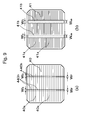
- solar cell 4 has front electrode 40 on the front surface thereof including a plurality of straight line-shaped finger electrodes 40a, 40a, ... having a narrow width which are disposed so as to cover an approximate overall area of the front surface, and two straight line-shaped bus bar electrodes 440b, 440b, consisting of sets of two and having a narrow width, which are connected to finger electrodes 40a, 40a. Furthermore, solar cell 4 has rear electrode 41 on the rear surface thereof including a plurality of straight line-shaped finger electrodes 41a, 41a, ... having a narrow width which are disposed so as to cover an approximate overall area of the rear surface, and two pieces of strip-shaped bus bar electrodes 41b having a wide width which are connected to finger electrodes 41a, 41a.
- bus bar electrode 440b of front electrode 40 is straight line-shaped, consists of sets of two, and has a narrow width, and other points are the same as the first embodiment.
- the amount of electrode materials can be suppressed and a cell fracture can be suppressed.
- a sixth embodiment of the invention is described mainly about a difference from the first embodiment.
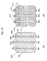
- front electrode 40 has three bus bar electrodes 40b, 40b, 40b
- rear electrode 41 has three bus bar electrodes 41b, 41b, 41b.
- the embodiment an advantageous effect similarly to that of the first embodiment can be obtained.
- the embodiment includes three bus bar electrodes on the front surface and the rear surface, respectively, an advantageous effect of increased power-collecting efficiency can be obtained.
- a seventh embodiment of the invention is described mainly about a difference from the first embodiment.
- front electrode 40 has a busbarless structure in which no bus bar electrode is included, and other points are the same.
- busbarless structure in a state where an adhesive made of a resin is soft, in a step in which front electrode 40 or/and bus bar electrode 41b of rear electrode 41 and conductive connection member 5 are pressure-pressed and connected to each other, the pressing pressure on front electrode 40 and bus bar electrodes 41b of rear electrode 41 is not applied vertically but non-uniformly, and the pressing pressure on the solar cell is concentrated in a narrow range.
- bus bar electrodes 41b of rear electrode 41 having a width equal to or more than a value of the width Ws of conductive connection member 5, preferably a value more than the value of Ws, function as reinforcing members, a cell fracture can be reduced, which leads to an improved manufacture yield.
- the embodiment also can obtain an advantageous effect similarly to that of the first embodiment.
- An eighth embodiment of the invention is described mainly about a difference from the first embodiment.
- the embodiment is different from the first embodiment in that, as shown in Fig. 12 , adjacent solar cells 4, 4 have an element configuration in which polarities thereof are reversed with each other.
- Connection members 5, 5, ... electrically connect in series between front electrodes 40 and 40 of adjacent solar cells 4, 4, and between rear electrodes 41 and 41 of solar cells 4, 4, respectively.
- the amount of electrode materials can be suppressed and a manufacture yield is good.
- a ninth embodiment of the invention is described mainly about a difference from the first embodiment.
- the embodiment is different from the first embodiment in that, as shown in Fig. 13 , adjacent two solar cells 4, 4 are disposed electrically in parallel as a pair.
- the amount of electrode materials can be suppressed and a manufacture yield is good.
- the solar cell system according to the embodiment is configured to include a plurality of solar cell modules 1 according to the first embodiment to the ninth embodiment, and a control system for controlling these solar cell modules.
- These solar cell modules are attached and fixed to roof faces, respectively, on a roof of a private house, for example, using fixing screws, and adjacent solar cell modules are engaged with each other, to install the solar cell modules in a thatched roof form (stepwise form) from the lower side (eaves side) toward the upper side (ridge side).
- the amount of electrode materials can be suppressed and a manufacture yield is good.
- the abovementioned solar cell system is a solar cell system for a private house, for example, however, the invention is not limited thereto. Furthermore, an install method of solar cell modules can be changed as appropriate.
- the solar cells according to the abovementioned respective embodiments are described by using a so-called HIT solar cell, however, can be used for various solar cells including a single crystalline solar cell, a polycrystalline solar cell, and the like, as appropriate, and can be applicable to a one-side light receiving type solar cell, in addition to a double-sided light receiving type solar cell.
- a solar cell may be used in which an n+ layer is formed from the front surface to a portion having a predetermined depth of a silicon substrate including a P-type polycrystalline or a P-type single crystalline to form a pn junction, a p+ layer is formed from the rear surface to a portion having a predetermined depth of the silicon substrate, front electrode 40 is formed on the n+ layer, and rear electrode 41 is formed on the p+ layer.
- the rear electrode is an electrode including finger electrodes and bus bar electrodes, however, can be applicable, for example, to an electrode in which a rear electrode has another structure, for example, a rear electrode including an electrode in which an entire surface thereof is covered with a metal film, and a bus bar electrode which is formed on this electrode.
- the solar cell module of the invention is not limited to the solar cell modules of the abovementioned respective embodiments, and for example, may be a configuration including no frame body.
- the solar cell module of the invention may be a double-sided type solar cell module, and for example, both a surface-side cover and a rear-side cover are made of glass plates.
- the front electrode and the rear electrode include two or three bus bar electrodes, respectively.
- the number thereof may be changed as appropriate.
Landscapes
- Photovoltaic Devices (AREA)
Abstract
Description
- The invention relates to a solar cell, a solar cell module, and a solar cell system.
- A solar cell system including solar cells is expected to be a new clean energy conversion system because of its capability of directly converting solar light into electricity, and has been increasingly utilized in a power supply for ordinary households and a power generation plant, in recent years.
- In such a situation, in order to get solar cell systems into widespread use, research and development for cost reduction and enhanced performance of solar cells, for example, are highly practiced.
- A conventional solar cell system includes, for example, one or a plurality of solar cell modules, and this solar cell module has a plurality of solar cells electrically connected to each other.
- In the conventional solar cell module, generally, a space between a front electrode of one solar cell of adjacent solar cells and a rear electrode of the other solar cell thereof is connected by a connection member having conductive properties such as a copper foil with solder interposed therebetween. In the solar cell, for example, the abovementioned front electrode includes a plurality of finger electrodes having a narrow width which are formed within a region of an approximate overall area of the front surface of the solar cell, and a bus bar electrode having a wide width which is connected to this finger electrode. Furthermore, the abovementioned rear electrode includes a plurality of finger electrodes having a narrow width which are formed within a region of an approximate overall area of the rear surface of the solar cell, and a bus bar electrode having a wide width which is connected to this finger electrode.
- Furthermore, a technique in which connection between the abovementioned conductive connection member and a front electrode or a rear electrode is achieved by a resin adhesive containing a resin is proposed recently. (For example, see Patent Literature 1).
- When connection between the conductive connection member and the abovementioned front electrode or rear electrode in the use of a resin adhesive, the connection between the connection member and the electrode can be achieved, without solder being fused as in the case of the conventional technique. Accordingly, a bus bar electrode can be formed to have a narrower width compared with the conventional bus bar electrode, thereby making it possible to reduce the amount of electrode materials and a cost.
-
- Patent Literature 1: Japanese Patent Application Publication No.
2008-147567 - However, if a bus bar electrode is formed to have a narrow width, in a step in which a connection member is pressure-pressed on and connected to a front electrode or a rear electrode, a pressing force applied on a solar cell via a bus bar electrode having a narrow width becomes larger compared with that of a bus bar electrode having a wide width. Furthermore, due to the cross section shape of the bus bar electrode having a narrow width or the pressing force mechanism, the pressing pressure on the bus bar electrode of the front electrode or the rear electrode is not applied to the front surface of the solar cell vertically but easily applies thereto non-uniformly. Accordingly, in a step in which the connection member is connected to the electrode, there is a fear that a fracture of the solar cell, a crack, or the like may be generated, and a manufacture yield may be reduced. In particular, the thinner the thickness of the substrate of the solar cell is, the more apparent this generation of a fracture or a crack in the solar cell becomes.
- The invention is made in view of the abovementioned problem, and provides a solar cell, a solar cell module, and a solar cell system good in a manufacture yield.
- A solar cell according to the invention is characterized in that the solar cell includes: a first principal-surface side electrode; and a second principal-surface side electrode, in which a connection member for solar cell connection is connected onto the first principal-surface side electrode and onto the second principal-surface side electrode. In the solar cell, the first principal-surface side electrode has a plurality of fine line-shaped electrodes and a connection electrode electrically connected to the plurality of fine line-shaped electrodes, and a width of the connection electrode on the first principal-surface side electrode is smaller than a width of the connection member, and the second principal-surface side electrode has a collector electrode and a connection electrode electrically connected to the collector electrode, and a width of the connection electrode on the second principal-surface side electrode is not less than a region width of the connection electrode on the first principal-surface side electrode.
- Note that, in the description, the region width of the connection electrode on the first principal-surface side electrode means a width or a width of the outline, of the connection electrode.
-
- [
Fig. 1] Fig. 1 is a top view of a solar cell module according to a first embodiment of the invention. - [
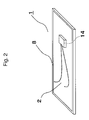
Fig. 2] Fig. 2 is a perspective view of the solar cell module according to the first embodiment of the invention. - [
Fig. 3] Fig. 3 is a partial cross-sectional view taken along the line A-A' inFig. 1 . - [
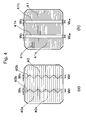
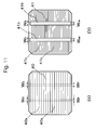
Fig. 4] Fig. 4(a) is a top view andFig. 4(b) is a rear view, of a solar cell according to the first embodiment. - [
Fig. 5] Fig. 5(a) is a top view of the solar cell for explaining connection between the solar cell and a connection member in the solar cell module according to the first embodiment of the invention, and -
Fig. 5 (b) is a partial cross-sectional view taken along the line A-A' inFig. 5(a) . - [
Fig. 6] Fig. 6(a) is a top view andFig. 6(b) is a bottom view, of a solar cell according to a second embodiment of the invention. - [
Fig. 7] Fig. 7(a) is a top view andFig. 7(b) is a bottom view, of a solar cell according to a third embodiment of the invention. - [
Fig. 8] Fig. 8(a) is a top view andFig. 8(b) is a bottom view, of a solar cell according to a fourth embodiment of the invention. - [
Fig. 9] Fig. 9(a) is a top view andFig. 9(b) is a bottom view, of a solar cell according to a fifth embodiment of the invention. - [
Fig. 10] Fig. 10 (a) is a top view andFig. 10 (b) is a bottom view, of a solar cell according to a sixth embodiment of the invention. - [
Fig. 11] Fig. 11 (a) is a top view andFig. 11 (b) is a bottom view, of a solar cell according to a seventh embodiment of the invention. - [
Fig. 12] Fig. 12 is a partial cross-sectional view of a solar cell module according to an eighth embodiment of the invention. - [
Fig. 13] Fig. 13 is a partial cross-sectional view of a solar cell module according to a ninth embodiment of the invention. - Next, embodiments of the invention are described using the drawings. In the description of the following drawings, the same or similar portions are donated with the same or similar reference numerals. However, it is noted that the drawings are schematic, and the ratio or the like of the respective dimensions is different from an actual one. Accordingly, specific dimensions and the like should be determined by considering the explanation below. Furthermore, naturally included are portions whose relations and ratios of the dimensions are different from each other between the drawings.
- A first embodiment of the invention is described with reference to
Fig. 1 to Fig. 5 . -
Solar cell module 1 comprisesfront cover 2,rear cover 3, a plurality ofsolar cells 4, andfiller 7. The plurality ofsolar cells 4 are electrically connected byconductive connection members 5. -
Front cover 2 is made of a translucent material, such as glass or translucent plastic, and allows the received solar light to pass through to the side ofsolar cells 4. Rearcover 3 is made of a material including a resin film, such as polyethylene terephthalate (PET), a resin film in which resin films are laminated such that a metal foil, such as an AI foil, is sandwiched therebetween, glass, or the like.Rear cover 3 may be translucent or non-translucent. - Filler 7 fills between
front cover 2 and the plurality ofsolar cells 4, betweenrear cover 3 and thesolar cells 4, and between adjacentsolar cells Filler 7 is made, for example, of a resin including an ethylene vinyl acetate copolymer resin (EVA) or the like. Note that, in the invention,filler 7 which is filled in the spaces betweenfront cover 2 and the plurality ofsolar cells 4, andfiller 7 which is filled in the spaces betweenrear cover 3 andsolar cells 4 are made of the same material, or made of materials different from each other. -
Connection member 5 can be configured using a copper foil with a surface thereof coated with a solder layer, for example, however, the form ofconnection member 5 in the invention is not limited thereto. - Furthermore,
solar cell module 1 is plate-shaped as a whole, and is attached withframe body 8 made of a metal such as aluminum on the outer circumference thereof if necessary. Furthermore,terminal box 14 for taking out an output fromsolar cell module 1 to the outside is attached to the surface ofrear cover 3. - The plurality of
solar cells 4 arranged in straight line shapes are electrically connected in series with each other byconnection members 5, and constitutesolar cell group 6 being line-shaped as a whole.Solar cell module 1 according to the embodiment has sixsolar cell groups 6.Solar cell groups 6 are disposed in parallel with each other. Accordingly, insolar cell module 1, the plurality ofsolar cells 4 are arranged in a matrix shape. -
Solar cell groups transition wiring First transition wiring 9 has a striped shape,second transition wiring 10 andthird transition wiring 11 each have an L-character shape.Second transition wiring 10 andthird transition wiring 11 each have a terminal portion for connecting to a bypass diode accommodated insideterminal box 14, on a tip of the L-character shaped wiring. First tothird transition wiring connection member 5, using a copper foil with a surface thereof coated with a solder layer, however, the form thereof is not limited thereto. - With the configuration as described above, all
solar cells 4 are electrically connected in series in the embodiment. Furthermore, among the plurality ofsolar cells 4 electrically connected in series, tosolar cells shaped extraction wiring Extraction wiring connection members 5, using a copper foil with a surface thereof coated with a solder layer, however, the form thereof is not limited thereto. - Note that, an insulating member including an insulating film such as polyethylene terephthalate (PET), an insulating resin such as an EVA, or the like is interposed in a portion where
second transition wiring 10 andextraction wiring 12 intersect each other, in order to prevent an undesired short circuit betweenmembers third transition wiring 11 andextraction wiring 13 intersect each other, in order to prevent an undesired short circuit betweenmembers - Furthermore, tip portions of second and
third transition wiring extraction wiring rear cover 3 to lead interminal box 14. Interminal box 14, bypass diodes are connected betweenextraction wiring 12 andsecond transition wiring 10, betweensecond transition wiring 10 andthird transition wiring 11, and betweenthird transition wiring 11 andextraction wiring 13, respectively. -
Solar cell 4 according to the embodiment is a crystalline solar cell having a crystalline semiconductor substrate such as a single crystalline silicon substrate or a polycrystalline silicon substrate. Examples ofsolar cell 4 include a hetero-junction type crystalline solar cell having an n-type single crystalline silicon substrate and a p-type amorphous semiconductor layer formed on the surface of this substrate, and a homo-junction type crystalline solar cell having a p-type polycrystalline silicon substrate and an n-type region formed on the surface of this substrate by heat diffusion. Furthermore, as a hetero-junction type crystalline solar cell, an HIT (Hetero-junction with Intrinsic Thin layer) junction type solar cell may be used, in which an i-type amorphous silicon layer having a thickness to the extent that does not substantially contribute power generation is interposed between the n-type single crystalline silicon substrate and the p-type amorphous silicon layer. - As shown in
Fig. 4 andFig. 5 ,solar cell 4 has a bifacial light receiving configuration capable of receiving light from both of the front and the rear. Note that, regions surrounded by the dashed line inFig. 4 indicate regions whereconnection members 5 are disposed. -
Front electrode 40 has a plurality offinger electrodes 40a disposed on an approximate overall area of the front surface ofsolar cell 4.Finger electrode 40a has an approximate straight-line shape, and the plurality offinger electrodes 40a are arranged in parallel with each other with a predetermined interval (for example, interval of 2 mm). The width offinger electrode 40a is within a range of 50 µm to 120 µm, and preferably a range of 50 µm to 100 µm. Furthermore, the thickness offinger electrode 40a is within a range of 20 µm to 60 µm. Among photogenerated carriers (electrons or positive holes) which are generated insolar cells 4 due to reception of light, the plurality offinger electrodes 40a collect one type of the photogenerated carriers. - Furthermore,
front electrode 40 hasbus bar electrodes 40b disposed so as to intersect allfinger electrodes 40b.Bus bar electrodes 40a collect electricity from the photogenerated carriers collected by the plurality offinger electrodes 40a.Bus bar electrode 40b has a zigzag line shape in which a plurality of straight lines are connected in a zigzag shape. The thickness ofbus bar electrode 40b is within a range of 20 µm to 80 µm.Bus bar electrode 40b may be formed through a step the same as that offinger electrode 40a. In this case, the thickness ofbus bar electrode 40b is equivalent to or slightly larger than the thickness offinger electrode 40a. Furthermore, the width ofbus bar electrode 40b is formed to be equivalent to or slightly wider than the width offinger electrode 40a. The width ofbus bar electrode 40b is within a range of 50 µm to 200 µm, and preferably within a range of 80 µm to 150 µm. Furthermore, a ratio Whf/Whb, which is a ratio of a line width Whf offinger electrode 40a to a line width Whb ofbus bar electrode 40b, is within a range of 0.3 to 2.5, and preferably a difference between the line width offinger electrode 40a and the line width ofbus bar electrode 40b is, for example, within an absolute value of 100 µm. - Furthermore, respective apexes (connection points) of zigzag-line shaped
bus bar electrode 40b are located outside from a region whereconnection member 5 is disposed (a region sandwiched by the dashed lines). Accordingly, whenconnection member 5 is connected, the respective apexes (connection points) of zigzag-line shapedbus bar electrode 40b and a vicinity thereof are exposed from theconnection member 5. In other words, the width between the apexes ofbus bar electrode 40b (the width of a region wherebus bar electrode 40b is disposed: Wr inFig. 4 ) is larger than the width of connection member 5 (Ws inFig. 4 ). The width of a region wherebus bar electrode 40b is disposed is set such that, even when a disposed position ofconnection member 5 is shifted due to a mechanical error,connection member 5 is disposed onbus bar electrode 40b reliably. For example, when the width Ws ofconnection members 5 is 1.0 mm to 1.2 mm, the width Wr of the region wherebus bar electrode 40b is disposed is set to 1.6 mm to 1.8 mm. - Note that, the number of
finger electrodes 40a and the number ofbus bar electrodes 40b can be set as appropriate in accordance with the size, physical properties, or the like, of the solar cell. For example, the number ofbus bar electrodes 40b is two inFig. 4 , however, the number ofbus bar electrodes 40b is not limited thereto and may be three or more. - Furthermore, in
front electrode 40,finger electrode 40a preferably has a width as narrow as possible in order to reduce a loss due to light blocking and ensure the sufficient incidence of light onsolar cell 4. For this purpose, whenfront electrode 40 is formed by screen printing, it is preferable to use the extend direction offinger electrode 40a as a printing direction. Furthermore, in order to prevent a print becoming faint ofbus bar electrode 40b from being generated, the line width ofbus bar electrode 40b is preferably set larger than the line width offinger electrode 40a. For example, the ratio Whf/Whb of the line width Whf offinger electrode 40a to the line width Whb ofbus bar electrode 40b is set to not less than 0.3 and less than 1. - Furthermore, in
front electrode 40 serving as a principal-surface side for receiving light, in order to achieve the low resistance and make reception of light by the solar cells be good,bus bar electrode 40b preferably has a narrow width thereof, and, in addition, the widths, that is the areas, offinger electrode 40a andbus bar electrode 40b are made small, while the thicknesses thereof are made large, compared with those ofrear electrode 41 described later. -
Rear electrode 41 has a plurality offinger electrodes 41a disposed on an approximate overall area of the rear surface ofsolar cell 4, andbus bar electrodes 41b.Finger electrodes 41a has an approximate straight-line shape, and the plurality offinger electrodes 41a are arranged in parallel with each other with a predetermined interval (for example, interval of 1 mm). Becausefinger electrode 41a at the rear side is not required to consider a light receiving loss, the width thereof is formed to be equivalent to or wider than the width offinger electrode 40a at the front side.Finger electrode 41a is formed to have a width from 50 µm to 200 µm, for example. Furthermore, the thickness offinger electrode 41a is within a range of 5 µm to 60 µm. Furthermore, the number offinger electrodes 41a at the rear side is formed greater in number than the number offinger electrodes 40a at the front side because no loss due to light blocking is required to be considered. Such a configuration makes it possible to reduce a resistance loss offinger electrodes 41a. Note that, the plurality offinger electrodes 41a collect, among photogenerated carriers (electrons or positive holes) which are generated insolar cells 4, the other type of the photogenerated carriers. -
Bus bar electrodes 41b are disposed so as to intersect allfinger electrodes 41a, and collect electricity from the photogenerated carriers collected the plurality offinger electrodes 41a.Bus bar electrode 41b at the rear side is formed in a straight line shape having a width wider than that offinger electrode 41a. Furthermore, a width Wub ofbus bar electrode 41b is larger than the width Ws ofconnection member 5. For example, when the width Ws ofconnection member 5 is from 1.0 mm to 1.2 mm, the width Wub of a region wherebus bar electrode 41b is disposed is set to from 1.6 mm to 1.8 mm. - Note that, the number of
bus bar electrodes 41b at the rear side is the same as the number ofbus bar electrodes 40b at the front side.Bus bar electrodes 41b andbus bar electrodes 40b are disposed at positions opposed to each other from the surface and rear sides ofsolar cell 4. Furthermore, the width Wr of a region wherebus bar electrode 40b at the front side is disposed is equivalent to the width Wub of a region wherebus bar electrode 41b at the rear side is disposed. - Note that, because an effect of the light-receiving amount on element characteristics is smaller in
rear electrode 41 compared with that infront electrode 40, the low resistance may be achieved by making the thickness ofrear electrode 41 be thinner than that offront electrode 40, and the widths, that is the areas, offinger electrode 41a andbus bar electrode 41b be large. - Furthermore,
solar cell 4 may have a transparent conductive film made of translucent conductive oxide such as indium oxide or zinc oxide, as a base offront electrode 40. Furthermore,solar cell 4 may have a transparent conductive film made of translucent conductive oxide such as indium oxide or zinc oxide, as a base ofrear electrode 41. -
Finger electrodes bus bar electrodes finger electrodes bus bar electrodes finger electrodes bus bar electrodes -
Wiring member 5 is connected tobus bar electrode 40b at the front side of onesolar cell 4 andbus bar electrodes 41b at the rear side of the othersolar cell 4, out of adjacentsolar cells resin adhesive 15. Specifically,wiring member 5 has an elongated shape, and one end portion side in the longitudinal direction is connected onto the surface ofbus bar electrode 40b byresin adhesive 15 and the other end portion side is connected onto the surface ofbus bar electrode 41b byresin adhesive 15. A resin component inresin adhesive 15 allowswiring member 5 to mechanically connect to the front surface or the rear surface ofsolar cells 4. Furthermore, direct contacts of the surfaces ofwiring member 5 to the surface ofbus bar electrode 40b and the surface ofbus bar electrode 41b allowwiring member 5 to be electrically connected tobus bar electrodes -
Resin adhesive 15 contains a resin. Furthermore,resin adhesive 15 has insulating properties or conductive properties. Examples of resin adhesive 15 having conductive properties include a resin adhesive with a resin having conductive particles. Examples of this resin adhesive include an anisotropic conductive adhesive. Note that, when conductive resin adhesive 15 containing conductive particles is used,wiring member 5 is also electrically connected tobus bar electrodes - In the embodiment,
connection member 5 hascoating layer 5a on the surface of a main body thereof made of a metal such as a copper foil. Coveringlayer 5a above is made of solder or a conductive material such as tin or silver. -
Fig. 5 shows an example in whichcoating layer 5a is made of a soft layer such as solder. Solder has a melting point from 230 to 260°C, for example.Resin adhesive 15 containing an epoxy-based resin and nickel particles which are conductive particles has a curing point at approximately 180°C. At the temperature at whichresin adhesive 15 is caused to cure,bus bar electrode 40b is harder thancoating layer 5a. In such a state, ifconnection member 5 is relatively pressure-pressed againstsolar cell 4, the tip ofbus bar electrode 40b is embedded intocoating layer 5a so thatbus bar electrode 40b is brought into direct contact with the surface ofconnection member 5. In this manner,connection member 5 andbus bar electrode 40b are electrically connected to each other. -
Resin adhesive 15 is present so as to spread over between, out of surfaces ofconnection member 5, the surface opposing to the front surface ofsolar cell 4, and the side surface ofbus bar electrode 40b. In this manner,connection member 5 is mechanically connected to the front surface ofsolar cell 4. In addition,resin adhesive 15 is present so as to spread out from, out of surfaces of theconnection members 5, the surface opposing to the front surface ofsolar cell 4, over the side surfacebus bar electrode 40b, across the front surface ofsolar cell 4. Such a configuration makes it possible to improve the connection strength ofconnection members 5. Note that, inFig. 5 ,resin adhesive 15 is present also on the side surfaces ofconnection member 5. Such a configuration makes it possible to further improve the connection strength ofconnection member 5. - Furthermore, at the rear surface of
solar cell 4, the surface ofcoating layer 5a on the surface of theconnection member 5 is brought into direct contact with the surface ofbus bar electrode 41b. In this manner,connection member 5 andbus bar electrode 41b are electrically connected to each other. Furthermore,resin adhesive 15 is present so as to spread over between the side surface ofconnection member 5 and the surface ofbus bar electrode 41b. In this manner,connection member 5 is mechanically connected to the rear surface ofsolar cell 4. Furthermore,resin adhesive 15 is present so as to spread out from the side surface ofconnection member 5, over the surface ofbus bar electrode 41b, across the side surface ofbus bar electrode 41b. Such a configuration makes it possible to improve the connectionstrength connection members 5. In addition,resin adhesive 15 is present so as to spread out from the side surface ofconnection member 5, over the surface ofbus bar electrode 41b and the side surface ofbus bar electrode 41b, across the rear surface ofsolar cell 4. Such a configuration makes it possible further to improve the connection strength ofconnection member 5. - Note that, an example in which a soft layer such as a solder layer is used as
coating layer 5a is shown inFig. 5 , however, the invention is not limited thereto. A metal harder than solder, such as silver, can be used ascoating layer 5a, orconnection member 5 including nocoating layer 5a can be also used. In this case, the tip of the bus bar electrode is brought into direct contact with the surface ofconnection member 5 without being embedded incoating layer 5a. Alternatively, the tip of the bus bar electrode of a deformed shape is brought into direct contact with the surface ofconnection member 5. Alternatively, the surface ofconnection member 5 is brought into direct contact with the bus bar electrode in a shape where a part thereof is embedded in the bus bar electrode. Such cases are also included in the invention. - In the embodiment, in a step in which
connection member 5 is relatively pressure-pressed on and connected tosolar cells 4, the pressing pressure onbus bar electrodes bus bar electrode 40b on the surface andbus bar electrode 41b on rear 1 function as reinforcing members, a fracture or a crack ofsolar cell 4 can be prevented from being generated, which leads to an improved manufacture yield. - In particular, the invention exhibits a prominent effect when a substrate included in
solar cell 4 has a small thickness. For example, a crystalline silicon substrate having a 200 µm or less thickness can be applied naturally, and a crystalline silicon substrate having a 150 µm or less thickness may be applied. In addition, a crystalline silicon substrate having a 100 µm or less thickness leads to a good manufacture yield. - Furthermore, the region width Wr of
bus bar electrode 40b and the region width Wub ofbus bar electrode 41b are larger than the width Ws ofconnection member 5. This enablesconnection member 5 to be reliably disposed on the surfaces ofbus bar electrodes connection member 5 is disposed is low. Accordingly, the manufacture time can be reduced and the manufacture cost can be reduced. - Furthermore,
front electrode 40 includes fine line-shapedfinger electrode 40a having a narrow width and fine line-shapedbus bar electrode 40b having a narrow width. Furthermore, becauserear electrode 41 includes fine line-shapedfinger electrodes 41a having a narrow width, the material amount of the electrodes can be reduced. In addition, making the thickness ofrear electrode 41 smaller can further reduce the material amount of the electrode. - Furthermore,
bus bar electrode 40b has a zigzag shape, that is, a non-linear shape such as a saw-edged shape which is not a straight line shape. Accordingly, a configuration in which a contact portion betweenconnection member 5 andbus bar electrode 40b is made larger is possible, compared with a case wherebus bar electrode 40b is a fine line-shaped and straight line shaped. Accordingly, a good electrical connection betweenfront electrode 40 andconnection member 5 can be obtained. Furthermore, because an undesired external force to be applied is distributed, in addition that a contact portion is made larger, a fracture or a crack ofsolar cell 4 can be prevented from being generated, thereby improving reliability of the mechanical connection. - Furthermore, because the region width Wr of
bus bar electrode 40b is larger than the width Ws ofconnection member 5, if resin adhesive 15 spreads out, an overhanging portion ofbus bar electrode 40b easily allows the spread to be captured within the portion. - A manufacturing method of a solar cell module according to the embodiment is described below.
- Firstly,
solar cell 4 including transparent electrode films on the front surface and the rear surface thereof is prepared. - Next, an epoxy-based thermosetting silver paste is printed on the transparent electrode film at the front side of
solar cell 4 by screen printing, the printed transparent electrode film is heated at 200°C for an hour and is cured, to formfront electrode 40. Then, similarly, an epoxy-based thermosetting silver paste is printed on the transparent electrode film at the rear side ofsolar cell 4 by screen printing, the printed transparent electrode film is heated at 200°C for an hour and is cured, to formrear electrode 41. - Next, a plurality of
connection members 5 are prepared.Paste resin adhesive 15 is applied to a portion on one surface of eachconnection member 5 opposing tosolar cell 4 and a portion on the other surface thereof opposing tosolar cell 4 adjacent tosolar cell 4 above such thatconnection member 5 have a thickness of approximately 30 µm, using a dispenser. Note that,resin adhesive 15 is not limited to be the paste resin adhesive, and a film-shaped resin adhesive may be used. - Next,
connection member 5 is disposed onbus bar electrode 40b offront electrode 40 of one solar cell and onbus bar electrode 41b ofrear electrode 41 of the othersolar cell solar cells resin adhesive 15 is applied are opposed to each other, is heated at 200°C for an hour while being pressure-pressed at the pressure of approximately 2 MPa to cureresin adhesive 15. In this manner,connection member 5 is connected to both of the front surface and the rear surface ofsolar cell 4. This step is repeated to produce the plurality ofsolar cell groups 6. - Next, the plurality of
solar cell groups 6 are electrically connected in series by first tothird transition wiring extraction wiring solar cells solar cells 4 are wired is produced,front cover 2, a filler sheet serving asfiller 7, the structure body, a filler sheet serving asfiller 7, andrear cover 3 are laminated in this order, and the laminated body thus obtained is heat press-bonded in a vacuum state at 150°C for 10 minutes. Then, the laminated body is heated at 150°C for one hour to cure the fillers perfectly. - Finally,
terminal box 14, andframe body 8 if necessary, are attached to the laminated body to completesolar cell module 1. - A second embodiment of the invention is described mainly about a difference from the first embodiment.
- As shown in
Fig. 6 , the second embodiment is different from the first embodiment is in that a region width Wr ofbus bar electrode 140b of front electrode 140 is equal to or narrower than the width Ws ofconnection member 5. Furthermore, the width of Wub ofbus bar electrodes 41b ofrear electrode 41 is configured so as to be equal to or larger than the width Ws ofconnection member 5, preferably larger than Ws, and equal to or larger than the region width Wr ofbus bar electrode 140b of front electrode 140, preferably larger than Wr. - For example, the region width Wr of
bus bar electrode 140b is set within a range of 0.6 mm to 1 mm, and the region width Wub ofbus bar electrode 41b is set within a range of 1 to 1.6 mm, to 1.6 mm for example. Other points are the same as the first embodiment. - In the embodiment, more accuracy in manufacturing is required compared with the first embodiment, however, a cell fracture can be suppressed and the electrode material can be reduced compared with the first embodiment.
- A third embodiment of the invention is described mainly about a difference from the first embodiment.
- As shown in
Fig. 7 ,solar cell 4 has afront electrode 40 on the front surface thereof including a plurality of straight line-shapedfinger electrodes 40a having a narrow width which are disposed so as to cover an approximate overall area of the surface, and two pieces of waveform-shapedbus bar electrodes 240b having a narrow width which are connected to fingerelectrodes 40a. Furthermore,solar cell 4 hasrear electrode 41 on the rear surface thereof including a plurality of straight line-shapedfinger electrodes 41a having a narrow width which are disposed so as to cover an approximate overall area of the rear surface, and two pieces of strip-shapedbus bar electrodes 41b having a wide width which are connected to fingerelectrodes 41a. - The embodiment is different from the first embodiment is in that bus bar electrode 240a of
front electrode 40 is waveform shaped, and other points are the same as the first embodiment. - The embodiment also can obtain an advantageous effect similarly to that of the first embodiment.
- A fourth embodiment of the invention is described mainly about a difference from the first embodiment.
- As shown in
Fig. 8 ,solar cell 4 has afront electrode 40 on the front surface thereof including a plurality of straight line-shapedfinger electrodes 40a having a narrow width which are disposed so as to cover an approximate overall area of the front surface, and two pieces of straight line-shapedbus bar electrodes 340b having a narrow width which are connected to fingerelectrodes 40a. Furthermore,solar cell 4 hasrear electrode 41 on the rear surface thereof including a plurality of straight line-shapedfinger electrodes 41a having a narrow width which are disposed so as to cover an approximate overall area of the rear surface, and two pieces of strip-shapedbus bar electrodes 41b having a wide width which are connected to fingerelectrodes 41a. - The embodiment is different from the first embodiment is in that the
bus bar electrode 340b offront electrode 40 is straight line-shaped, and a region width Wr ofbus bar electrode 340b is equal to the width Whb. - In the embodiment,
bus bar electrode 340b offront electrode 40 is fine line-shaped similarly tofinger electrode 40a, and a width Whb thereof is configured to be smaller than the width Ws ofconductive connection member 5. - Furthermore,
rear electrode 41 is configured such that the width Wub ofbus bar electrode 41b is larger than the region width Wr ofbus bar electrode 340b and equal to or larger than the width Ws ofconductive connection member 5, and preferably larger than the width Ws ofconductive connection member 5. - With the embodiment, electrode materials can be reduced and a cell fracture can be suppressed compared with the first embodiment.
- A fifth embodiment of the invention is described mainly about a difference from the first embodiment.
- As shown in
Fig. 9 ,solar cell 4 hasfront electrode 40 on the front surface thereof including a plurality of straight line-shapedfinger electrodes bus bar electrodes electrodes solar cell 4 hasrear electrode 41 on the rear surface thereof including a plurality of straight line-shapedfinger electrodes bus bar electrodes 41b having a wide width which are connected to fingerelectrodes - The embodiment is different from the first embodiment is in that
bus bar electrode 440b offront electrode 40 is straight line-shaped, consists of sets of two, and has a narrow width, and other points are the same as the first embodiment. - Also with the embodiment, the amount of electrode materials can be suppressed and a cell fracture can be suppressed.
- A sixth embodiment of the invention is described mainly about a difference from the first embodiment.
- The embodiment is different from the first embodiment in that, as shown in
Fig. 10 ,front electrode 40 has threebus bar electrodes rear electrode 41 has threebus bar electrodes - With the embodiment, an advantageous effect similarly to that of the first embodiment can be obtained. In addition, because the embodiment includes three bus bar electrodes on the front surface and the rear surface, respectively, an advantageous effect of increased power-collecting efficiency can be obtained.
- A seventh embodiment of the invention is described mainly about a difference from the first embodiment.
- The embodiment is different from the first embodiment in that, as shown in
Fig. 11 ,front electrode 40 has a busbarless structure in which no bus bar electrode is included, and other points are the same. - With such a busbarless structure, in a state where an adhesive made of a resin is soft, in a step in which
front electrode 40 or/andbus bar electrode 41b ofrear electrode 41 andconductive connection member 5 are pressure-pressed and connected to each other, the pressing pressure onfront electrode 40 andbus bar electrodes 41b ofrear electrode 41 is not applied vertically but non-uniformly, and the pressing pressure on the solar cell is concentrated in a narrow range. Even in this case, becausebus bar electrodes 41b ofrear electrode 41 having a width equal to or more than a value of the width Ws ofconductive connection member 5, preferably a value more than the value of Ws, function as reinforcing members, a cell fracture can be reduced, which leads to an improved manufacture yield. - The embodiment also can obtain an advantageous effect similarly to that of the first embodiment.
- An eighth embodiment of the invention is described mainly about a difference from the first embodiment.
- The embodiment is different from the first embodiment in that, as shown in
Fig. 12 , adjacentsolar cells Connection members front electrodes solar cells rear electrodes solar cells - Also with the embodiment, the amount of electrode materials can be suppressed and a manufacture yield is good.
- A ninth embodiment of the invention is described mainly about a difference from the first embodiment.
- The embodiment is different from the first embodiment in that, as shown in
Fig. 13 , adjacent twosolar cells - Also with the embodiment, the amount of electrode materials can be suppressed and a manufacture yield is good.
- Next, a solar cell system according to a tenth embodiment of the invention is described.
- The solar cell system according to the embodiment is configured to include a plurality of
solar cell modules 1 according to the first embodiment to the ninth embodiment, and a control system for controlling these solar cell modules. These solar cell modules are attached and fixed to roof faces, respectively, on a roof of a private house, for example, using fixing screws, and adjacent solar cell modules are engaged with each other, to install the solar cell modules in a thatched roof form (stepwise form) from the lower side (eaves side) toward the upper side (ridge side). - With the solar cell system according to the embodiment, the amount of electrode materials can be suppressed and a manufacture yield is good.
- The abovementioned solar cell system is a solar cell system for a private house, for example, however, the invention is not limited thereto. Furthermore, an install method of solar cell modules can be changed as appropriate.
- The solar cells according to the abovementioned respective embodiments are described by using a so-called HIT solar cell, however, can be used for various solar cells including a single crystalline solar cell, a polycrystalline solar cell, and the like, as appropriate, and can be applicable to a one-side light receiving type solar cell, in addition to a double-sided light receiving type solar cell.
- As for the abovementioned polycrystalline solar cell or single crystalline solar cell, for example, a solar cell may be used in which an n+ layer is formed from the front surface to a portion having a predetermined depth of a silicon substrate including a P-type polycrystalline or a P-type single crystalline to form a pn junction, a p+ layer is formed from the rear surface to a portion having a predetermined depth of the silicon substrate,
front electrode 40 is formed on the n+ layer, andrear electrode 41 is formed on the p+ layer. - In the abovementioned respective embodiments, the rear electrode is an electrode including finger electrodes and bus bar electrodes, however, can be applicable, for example, to an electrode in which a rear electrode has another structure, for example, a rear electrode including an electrode in which an entire surface thereof is covered with a metal film, and a bus bar electrode which is formed on this electrode.
- In addition, the solar cell module of the invention is not limited to the solar cell modules of the abovementioned respective embodiments, and for example, may be a configuration including no frame body.
- Furthermore, the solar cell module of the invention may be a double-sided type solar cell module, and for example, both a surface-side cover and a rear-side cover are made of glass plates.
- In addition, in the abovementioned respective embodiments, the front electrode and the rear electrode include two or three bus bar electrodes, respectively. However, the number thereof may be changed as appropriate.
- 1
- solar cell module
- 4
- solar cell
- 5
- connection member
- 40
- front electrode (principal-surface side electrode)
- 40a
- finger electrode
- 40b, 140b, 240b, 340b, 440b
- bus bar electrode (connection electrode)
- 41
- rear electrode (principal-surface side electrode)
- 41a
- finger electrode (collector electrode)
- 41b, 141b, 241b, 341b, 441b
- bus bar electrode (connection electrode)
Claims (13)
- A solar cell comprising:a first principal-surface side electrode; anda second principal-surface side electrode, in which a connection member for solar cell connection is connected onto the first principal-surface side electrode and onto the second principal-surface side electrode, whereinthe first principal-surface side electrode comprises a plurality of fine line-shaped electrodes and a connection electrode electrically connected to the plurality of fine line-shaped electrodes, a width of the connection electrode on the first principal-surface side electrode is smaller than a width of the connection member, andthe second principal-surface side electrode comprises a collector electrode and a connection electrode electrically connected to the collector electrode, a width of the connection electrode on the second principal-surface side electrode is not less than a region width of the connection electrode on the first principal-surface side electrode.
- The solar cell according to claim 1, characterized in that the connection electrode on the first principal-surface side electrode has a non-linear-shaped pattern.
- The solar cell according to claim 1, characterized in that the region width of the connection electrode on the first principal-surface side electrode is not less than the width of the connection member.
- The solar cell according to claim 1, characterized in that the connection member is connected to the first principal-surface side electrode and the second principal-surface side electrode by an adhesive containing a resin.
- A solar cell comprising:a first principal-surface side electrode; anda second principal-surface side electrode, in which a connection member for solar cell connection is connected onto the first principal-surface side electrode and onto the second principal-surface side electrode, whereinthe first principal-surface side electrode comprises a plurality of fine line-shaped electrodes;the second principal-surface side electrode comprises a collector electrode and a connection electrode electrically connected to the collector electrode; anda width of the connection electrode on the second principal-surface side electrode is not less than a width of the connection member.
- The solar cell according to claim 5, characterized in that the connection member is connected to the first principal-surface side electrode and the second principal-surface side electrode by an adhesive containing a resin.
- A solar cell module comprising:a solar cell including a first principal-surface side electrode and a second principal-surface side electrode; anda connection member for solar cell connection which is connected onto the first principal-surface side electrode and onto the second principal-surface side electrode, whereinthe first principal-surface side electrode comprises a plurality of fine line-shaped electrodes and a connection electrode electrically connected to the plurality of fine line-shaped electrodes, a width of the connection electrode on the first principal-surface side electrode is smaller than a width of the connection member, andthe second principal-surface side electrode comprises a collector electrode and a connection electrode electrically connected to the collector electrode, a width of the connection electrode on the second principal-surface side electrode is not less than a region width of the connection electrode on the first principal-surface side electrode.
- The solar cell module according to claim 7, characterized in that the connection electrode on the first principal-surface side electrode has a non-linear-shaped pattern.
- The solar cell module according to claim 7, characterized in that the region width of the connection electrode on the first principal-surface side electrode is not less than the width of the connection member.
- The solar cell module according to claim 7, characterized in that the connection member is connected to the first principal-surface side electrode and the second principal-surface side electrode by an adhesive containing a resin.
- A solar cell module comprising:a solar cell comprising a first principal-surface side electrode and a second principal-surface side electrode; anda connection member for solar cell connection which is connected onto the first principal-surface side electrode and onto the second principal-surface side electrode, whereinthe first principal-surface side electrode comprises a plurality of fine line-shaped electrodes;the second principal-surface side electrode comprises a collector electrode and a connection electrode electrically connected to the collector electrode; anda width of the connection electrode on the second principal-surface side electrode is not less than a width of the connection member.
- The solar cell module according to claim 11, characterized in that the connection member is connected to the first principal-surface side electrode and the second principal-surface side electrode by an adhesive containing a resin.
- A solar cell system, characterized in that the solar cell system comprises the solar cell module according to claim 7.
Applications Claiming Priority (2)
| Application Number | Priority Date | Filing Date | Title |
|---|---|---|---|
| JP2009189730 | 2009-08-19 | ||
| PCT/JP2010/063969 WO2011021655A1 (en) | 2009-08-19 | 2010-08-19 | Solar battery, solar battery module and solar battery system |
Publications (3)
| Publication Number | Publication Date |
|---|---|
| EP2469604A1 true EP2469604A1 (en) | 2012-06-27 |
| EP2469604A4 EP2469604A4 (en) | 2017-11-22 |
| EP2469604B1 EP2469604B1 (en) | 2019-10-09 |
Family
ID=43607106
Family Applications (1)
| Application Number | Title | Priority Date | Filing Date |
|---|---|---|---|
| EP10809996.1A Active EP2469604B1 (en) | 2009-08-19 | 2010-08-19 | Solar battery module |
Country Status (6)
| Country | Link |
|---|---|
| US (2) | US20120305047A1 (en) |
| EP (1) | EP2469604B1 (en) |
| JP (1) | JP5648638B2 (en) |
| KR (1) | KR101679452B1 (en) |
| CN (1) | CN102576750B (en) |
| WO (1) | WO2011021655A1 (en) |
Cited By (1)
| Publication number | Priority date | Publication date | Assignee | Title |
|---|---|---|---|---|
| EP2924740A4 (en) * | 2012-11-21 | 2016-07-27 | Choshu Industry Co Ltd | PHOTOVOLTAIC DEVICE |
Families Citing this family (25)
| Publication number | Priority date | Publication date | Assignee | Title |
|---|---|---|---|---|
| JP5377409B2 (en) * | 2010-05-28 | 2013-12-25 | 三洋電機株式会社 | Solar cell module and manufacturing method thereof |
| WO2012002216A1 (en) * | 2010-06-30 | 2012-01-05 | 三洋電機株式会社 | Solar cell module |
| KR101661768B1 (en) | 2010-09-03 | 2016-09-30 | 엘지전자 주식회사 | Solar cell and manufacturing method thereof |
| CN102683325B (en) | 2011-03-08 | 2018-06-15 | 日立化成株式会社 | Solar battery cell |
| US9455359B2 (en) | 2011-05-31 | 2016-09-27 | Hitachi Chemical Company, Ltd. | Solar battery cell, solar battery module and method of making solar battery module |
| KR20120140026A (en) * | 2011-06-20 | 2012-12-28 | 엘지전자 주식회사 | Solar cell |
| JP5967512B2 (en) * | 2011-06-30 | 2016-08-10 | パナソニックIpマネジメント株式会社 | Solar cell module |
| CN103022201A (en) * | 2011-09-27 | 2013-04-03 | 杜邦公司 | Crystal silicon solar battery module and manufacturing method thereof |
| CN102361038A (en) * | 2011-10-11 | 2012-02-22 | 润峰电力有限公司 | Novel main gate electrode of crystalline silicon solar battery |
| EP2787539A4 (en) * | 2011-11-30 | 2015-06-10 | Sanyo Electric Co | PHOTOVOLTAIC MODULE AND METHOD FOR MANUFACTURING THE SAME |
| JPWO2013080324A1 (en) * | 2011-11-30 | 2015-04-27 | 三洋電機株式会社 | Photovoltaic module and manufacturing method thereof |
| KR101838278B1 (en) * | 2011-12-23 | 2018-03-13 | 엘지전자 주식회사 | Solar cell |
| CN102610668A (en) * | 2012-03-15 | 2012-07-25 | 晶澳(扬州)太阳能科技有限公司 | Improved electrode structure of solar cell |
| KR101835118B1 (en) | 2012-03-16 | 2018-03-08 | 주성엔지니어링(주) | A solar cell and a manufacturing method thereof |
| JP6124166B2 (en) * | 2013-03-28 | 2017-05-10 | パナソニックIpマネジメント株式会社 | Solar cell module and method for manufacturing solar cell module |
| JP6326890B2 (en) * | 2013-04-30 | 2018-05-23 | 日立化成株式会社 | Manufacturing method of solar cell module |
| JP6410106B2 (en) * | 2013-05-28 | 2018-10-24 | パナソニックIpマネジメント株式会社 | Solar cell module |
| WO2015083148A1 (en) * | 2013-12-04 | 2015-06-11 | Utilight Ltd. | Solar cell bus bars |
| EP4210116A1 (en) * | 2014-07-07 | 2023-07-12 | Shangrao Jinko solar Technology Development Co., LTD | Solar cell module |
| US10651321B2 (en) * | 2015-01-29 | 2020-05-12 | Solaria Corporation | Solar module having a plurality of strings configured from a five strip cell |
| CN107980179B (en) * | 2015-08-13 | 2020-10-16 | 3M创新有限公司 | Photovoltaic cell with front bus tape on narrow front bus |
| WO2018159117A1 (en) * | 2017-03-03 | 2018-09-07 | 株式会社カネカ | Solar battery module |
| GB202020731D0 (en) * | 2020-12-30 | 2021-02-10 | Rec Solar Pte Ltd | A solar cell assembly |
| EP4064368A1 (en) | 2021-03-24 | 2022-09-28 | Sunpower Corporation | Cross-tied photovoltaic array |
| US11923473B1 (en) * | 2022-12-06 | 2024-03-05 | Maxeon Solar Pte. Ltd. | Shingled solar module with ribbon interconnect |
Family Cites Families (13)
| Publication number | Priority date | Publication date | Assignee | Title |
|---|---|---|---|---|
| JP3743743B2 (en) * | 1999-03-09 | 2006-02-08 | 三菱電機株式会社 | Solar cell |
| JP3566901B2 (en) * | 2000-03-28 | 2004-09-15 | シャープ株式会社 | Solar cell manufacturing method |
| JP4153785B2 (en) * | 2002-12-19 | 2008-09-24 | 京セラ株式会社 | Solar cell module |
| JP4502845B2 (en) * | 2005-02-25 | 2010-07-14 | 三洋電機株式会社 | Photovoltaic element |
| US20070235077A1 (en) * | 2006-03-27 | 2007-10-11 | Kyocera Corporation | Solar Cell Module and Manufacturing Process Thereof |
| JP4294048B2 (en) * | 2006-11-29 | 2009-07-08 | 三洋電機株式会社 | Solar cell module |
| JP5063099B2 (en) * | 2006-12-13 | 2012-10-31 | 三洋電機株式会社 | Solar cell module and method for manufacturing solar cell module |
| JP4974722B2 (en) * | 2007-03-16 | 2012-07-11 | 三洋電機株式会社 | Solar cell module manufacturing method and solar cell module |
| EP2020688B1 (en) * | 2007-08-02 | 2013-11-27 | Sanyo Electric Co., Ltd. | Solar cell interconnection using thermo-compression bonding and correspondingly fabricated module |
| JP4463297B2 (en) * | 2007-08-07 | 2010-05-19 | 三洋電機株式会社 | Solar cell module |
| KR100953618B1 (en) | 2008-01-11 | 2010-04-20 | 삼성에스디아이 주식회사 | Solar cell |
| JP5147672B2 (en) * | 2008-01-31 | 2013-02-20 | 三洋電機株式会社 | Solar cell module and method for manufacturing solar cell module |
| JPWO2010116914A1 (en) * | 2009-04-09 | 2012-10-18 | 三洋電機株式会社 | Solar cell and solar cell module |
-
2010
- 2010-08-19 WO PCT/JP2010/063969 patent/WO2011021655A1/en not_active Ceased
- 2010-08-19 EP EP10809996.1A patent/EP2469604B1/en active Active
- 2010-08-19 JP JP2011527695A patent/JP5648638B2/en not_active Expired - Fee Related
- 2010-08-19 KR KR1020127006864A patent/KR101679452B1/en not_active Expired - Fee Related
- 2010-08-19 CN CN201080046570.4A patent/CN102576750B/en not_active Expired - Fee Related
-
2012
- 2012-02-17 US US13/399,624 patent/US20120305047A1/en not_active Abandoned
-
2015
- 2015-03-31 US US14/673,933 patent/US20150206995A1/en not_active Abandoned
Non-Patent Citations (1)
| Title |
|---|
| See references of WO2011021655A1 * |
Cited By (1)
| Publication number | Priority date | Publication date | Assignee | Title |
|---|---|---|---|---|
| EP2924740A4 (en) * | 2012-11-21 | 2016-07-27 | Choshu Industry Co Ltd | PHOTOVOLTAIC DEVICE |
Also Published As
| Publication number | Publication date |
|---|---|
| US20120305047A1 (en) | 2012-12-06 |
| CN102576750A (en) | 2012-07-11 |
| WO2011021655A1 (en) | 2011-02-24 |
| EP2469604A4 (en) | 2017-11-22 |
| EP2469604B1 (en) | 2019-10-09 |
| CN102576750B (en) | 2015-01-07 |
| JP5648638B2 (en) | 2015-01-07 |
| US20150206995A1 (en) | 2015-07-23 |
| KR101679452B1 (en) | 2016-11-24 |
| KR20120049339A (en) | 2012-05-16 |
| JPWO2011021655A1 (en) | 2013-01-24 |
Similar Documents
| Publication | Publication Date | Title |
|---|---|---|
| EP2469604B1 (en) | Solar battery module | |
| JP5515367B2 (en) | Solar cell, solar cell module and solar cell system | |
| EP1928027B1 (en) | Solar cell module | |
| KR101535297B1 (en) | Solar cell module | |
| CN102790110B (en) | Solar cell module | |
| KR20100019389A (en) | Solar cell module | |
| JP5279334B2 (en) | Solar cell module | |
| EP2738816B1 (en) | Solar cell, solar cell module, and method for producing solar cell | |
| US20160079459A1 (en) | Solar cell module | |
| US10014426B2 (en) | Solar cell and solar cell module | |
| US20120216860A1 (en) | Interconnection sheet, solar cell with interconnection sheet, solar cell module, and interconnection sheet roll | |
| US20190123229A1 (en) | Solar cell module | |
| EP2579319A1 (en) | Solar cell module and solar cell | |
| EP3403283B1 (en) | Method for interconnecting solar cells | |
| EP2418689B1 (en) | Solar cell panel | |
| CN110707167A (en) | Back contact solar cell module production method and back contact solar cell module | |
| JP5203176B2 (en) | Wiring sheet, solar cell with wiring sheet and solar cell module | |
| US10622502B1 (en) | Solar cell edge interconnects | |
| JP2010238938A (en) | Solar cell, solar cell module and solar cell system | |
| JP7530221B2 (en) | Solar cell strings and solar cell modules | |
| EP2533295B1 (en) | Solar cell module | |
| WO2020031574A1 (en) | Solar cell module | |
| JP5381809B2 (en) | Solar cell module | |
| JP7482708B2 (en) | Solar Cells and Modules | |
| US9853170B2 (en) | Solar cell module manufacturing method |
Legal Events
| Date | Code | Title | Description |
|---|---|---|---|
| PUAI | Public reference made under article 153(3) epc to a published international application that has entered the european phase |
Free format text: ORIGINAL CODE: 0009012 |
|
| 17P | Request for examination filed |
Effective date: 20120313 |
|
| AK | Designated contracting states |
Kind code of ref document: A1 Designated state(s): AL AT BE BG CH CY CZ DE DK EE ES FI FR GB GR HR HU IE IS IT LI LT LU LV MC MK MT NL NO PL PT RO SE SI SK SM TR |
|
| DAX | Request for extension of the european patent (deleted) | ||
| RAP1 | Party data changed (applicant data changed or rights of an application transferred) |
Owner name: PANASONIC INTELLECTUAL PROPERTY MANAGEMENT CO., LT |
|
| RA4 | Supplementary search report drawn up and despatched (corrected) |
Effective date: 20171019 |
|
| RIC1 | Information provided on ipc code assigned before grant |
Ipc: H01L 31/05 20140101ALI20171013BHEP Ipc: H01L 31/04 20140101AFI20171013BHEP Ipc: H01L 31/0224 20060101ALI20171013BHEP |
|
| RIC1 | Information provided on ipc code assigned before grant |
Ipc: H01L 31/05 20140101ALI20190109BHEP Ipc: H01L 31/04 20140101AFI20190109BHEP Ipc: H01L 31/0224 20060101ALI20190109BHEP |
|
| GRAP | Despatch of communication of intention to grant a patent |
Free format text: ORIGINAL CODE: EPIDOSNIGR1 |
|
| STAA | Information on the status of an ep patent application or granted ep patent |
Free format text: STATUS: GRANT OF PATENT IS INTENDED |
|
| INTG | Intention to grant announced |
Effective date: 20190325 |
|
| RIN1 | Information on inventor provided before grant (corrected) |
Inventor name: KANNOU, HIROYUKI Inventor name: TAIRA, SHIGEHARU |
|
| GRAS | Grant fee paid |
Free format text: ORIGINAL CODE: EPIDOSNIGR3 |
|
| GRAA | (expected) grant |
Free format text: ORIGINAL CODE: 0009210 |
|
| STAA | Information on the status of an ep patent application or granted ep patent |
Free format text: STATUS: THE PATENT HAS BEEN GRANTED |
|
| AK | Designated contracting states |
Kind code of ref document: B1 Designated state(s): AL AT BE BG CH CY CZ DE DK EE ES FI FR GB GR HR HU IE IS IT LI LT LU LV MC MK MT NL NO PL PT RO SE SI SK SM TR |
|
| REG | Reference to a national code |
Ref country code: GB Ref legal event code: FG4D |
|
| REG | Reference to a national code |
Ref country code: CH Ref legal event code: EP |
|
| REG | Reference to a national code |
Ref country code: DE Ref legal event code: R096 Ref document number: 602010061454 Country of ref document: DE |
|
| REG | Reference to a national code |
Ref country code: IE Ref legal event code: FG4D |
|
| REG | Reference to a national code |
Ref country code: AT Ref legal event code: REF Ref document number: 1189821 Country of ref document: AT Kind code of ref document: T Effective date: 20191115 |
|
| REG | Reference to a national code |
Ref country code: NL Ref legal event code: MP Effective date: 20191009 |
|
| REG | Reference to a national code |
Ref country code: LT Ref legal event code: MG4D |
|
| REG | Reference to a national code |
Ref country code: AT Ref legal event code: MK05 Ref document number: 1189821 Country of ref document: AT Kind code of ref document: T Effective date: 20191009 |
|
| PG25 | Lapsed in a contracting state [announced via postgrant information from national office to epo] |
Ref country code: GR Free format text: LAPSE BECAUSE OF FAILURE TO SUBMIT A TRANSLATION OF THE DESCRIPTION OR TO PAY THE FEE WITHIN THE PRESCRIBED TIME-LIMIT Effective date: 20200110 Ref country code: ES Free format text: LAPSE BECAUSE OF FAILURE TO SUBMIT A TRANSLATION OF THE DESCRIPTION OR TO PAY THE FEE WITHIN THE PRESCRIBED TIME-LIMIT Effective date: 20191009 Ref country code: PT Free format text: LAPSE BECAUSE OF FAILURE TO SUBMIT A TRANSLATION OF THE DESCRIPTION OR TO PAY THE FEE WITHIN THE PRESCRIBED TIME-LIMIT Effective date: 20200210 Ref country code: LV Free format text: LAPSE BECAUSE OF FAILURE TO SUBMIT A TRANSLATION OF THE DESCRIPTION OR TO PAY THE FEE WITHIN THE PRESCRIBED TIME-LIMIT Effective date: 20191009 Ref country code: SE Free format text: LAPSE BECAUSE OF FAILURE TO SUBMIT A TRANSLATION OF THE DESCRIPTION OR TO PAY THE FEE WITHIN THE PRESCRIBED TIME-LIMIT Effective date: 20191009 Ref country code: PL Free format text: LAPSE BECAUSE OF FAILURE TO SUBMIT A TRANSLATION OF THE DESCRIPTION OR TO PAY THE FEE WITHIN THE PRESCRIBED TIME-LIMIT Effective date: 20191009 Ref country code: NO Free format text: LAPSE BECAUSE OF FAILURE TO SUBMIT A TRANSLATION OF THE DESCRIPTION OR TO PAY THE FEE WITHIN THE PRESCRIBED TIME-LIMIT Effective date: 20200109 Ref country code: LT Free format text: LAPSE BECAUSE OF FAILURE TO SUBMIT A TRANSLATION OF THE DESCRIPTION OR TO PAY THE FEE WITHIN THE PRESCRIBED TIME-LIMIT Effective date: 20191009 Ref country code: FI Free format text: LAPSE BECAUSE OF FAILURE TO SUBMIT A TRANSLATION OF THE DESCRIPTION OR TO PAY THE FEE WITHIN THE PRESCRIBED TIME-LIMIT Effective date: 20191009 Ref country code: BG Free format text: LAPSE BECAUSE OF FAILURE TO SUBMIT A TRANSLATION OF THE DESCRIPTION OR TO PAY THE FEE WITHIN THE PRESCRIBED TIME-LIMIT Effective date: 20200109 Ref country code: NL Free format text: LAPSE BECAUSE OF FAILURE TO SUBMIT A TRANSLATION OF THE DESCRIPTION OR TO PAY THE FEE WITHIN THE PRESCRIBED TIME-LIMIT Effective date: 20191009 Ref country code: AT Free format text: LAPSE BECAUSE OF FAILURE TO SUBMIT A TRANSLATION OF THE DESCRIPTION OR TO PAY THE FEE WITHIN THE PRESCRIBED TIME-LIMIT Effective date: 20191009 |
|
| PG25 | Lapsed in a contracting state [announced via postgrant information from national office to epo] |
Ref country code: IS Free format text: LAPSE BECAUSE OF FAILURE TO SUBMIT A TRANSLATION OF THE DESCRIPTION OR TO PAY THE FEE WITHIN THE PRESCRIBED TIME-LIMIT Effective date: 20200224 Ref country code: HR Free format text: LAPSE BECAUSE OF FAILURE TO SUBMIT A TRANSLATION OF THE DESCRIPTION OR TO PAY THE FEE WITHIN THE PRESCRIBED TIME-LIMIT Effective date: 20191009 |
|
| PG25 | Lapsed in a contracting state [announced via postgrant information from national office to epo] |
Ref country code: AL Free format text: LAPSE BECAUSE OF FAILURE TO SUBMIT A TRANSLATION OF THE DESCRIPTION OR TO PAY THE FEE WITHIN THE PRESCRIBED TIME-LIMIT Effective date: 20191009 |
|
| REG | Reference to a national code |
Ref country code: DE Ref legal event code: R097 Ref document number: 602010061454 Country of ref document: DE |
|
| PG2D | Information on lapse in contracting state deleted |
Ref country code: IS |
|
| PG25 | Lapsed in a contracting state [announced via postgrant information from national office to epo] |
Ref country code: EE Free format text: LAPSE BECAUSE OF FAILURE TO SUBMIT A TRANSLATION OF THE DESCRIPTION OR TO PAY THE FEE WITHIN THE PRESCRIBED TIME-LIMIT Effective date: 20191009 Ref country code: DK Free format text: LAPSE BECAUSE OF FAILURE TO SUBMIT A TRANSLATION OF THE DESCRIPTION OR TO PAY THE FEE WITHIN THE PRESCRIBED TIME-LIMIT Effective date: 20191009 Ref country code: RO Free format text: LAPSE BECAUSE OF FAILURE TO SUBMIT A TRANSLATION OF THE DESCRIPTION OR TO PAY THE FEE WITHIN THE PRESCRIBED TIME-LIMIT Effective date: 20191009 Ref country code: CZ Free format text: LAPSE BECAUSE OF FAILURE TO SUBMIT A TRANSLATION OF THE DESCRIPTION OR TO PAY THE FEE WITHIN THE PRESCRIBED TIME-LIMIT Effective date: 20191009 Ref country code: IS Free format text: LAPSE BECAUSE OF FAILURE TO SUBMIT A TRANSLATION OF THE DESCRIPTION OR TO PAY THE FEE WITHIN THE PRESCRIBED TIME-LIMIT Effective date: 20200209 |
|
| PLBE | No opposition filed within time limit |
Free format text: ORIGINAL CODE: 0009261 |
|
| STAA | Information on the status of an ep patent application or granted ep patent |
Free format text: STATUS: NO OPPOSITION FILED WITHIN TIME LIMIT |
|
| PG25 | Lapsed in a contracting state [announced via postgrant information from national office to epo] |
Ref country code: SM Free format text: LAPSE BECAUSE OF FAILURE TO SUBMIT A TRANSLATION OF THE DESCRIPTION OR TO PAY THE FEE WITHIN THE PRESCRIBED TIME-LIMIT Effective date: 20191009 Ref country code: SK Free format text: LAPSE BECAUSE OF FAILURE TO SUBMIT A TRANSLATION OF THE DESCRIPTION OR TO PAY THE FEE WITHIN THE PRESCRIBED TIME-LIMIT Effective date: 20191009 Ref country code: IT Free format text: LAPSE BECAUSE OF FAILURE TO SUBMIT A TRANSLATION OF THE DESCRIPTION OR TO PAY THE FEE WITHIN THE PRESCRIBED TIME-LIMIT Effective date: 20191009 |
|
| 26N | No opposition filed |
Effective date: 20200710 |
|
| PG25 | Lapsed in a contracting state [announced via postgrant information from national office to epo] |
Ref country code: SI Free format text: LAPSE BECAUSE OF FAILURE TO SUBMIT A TRANSLATION OF THE DESCRIPTION OR TO PAY THE FEE WITHIN THE PRESCRIBED TIME-LIMIT Effective date: 20191009 |
|
| PG25 | Lapsed in a contracting state [announced via postgrant information from national office to epo] |
Ref country code: MC Free format text: LAPSE BECAUSE OF FAILURE TO SUBMIT A TRANSLATION OF THE DESCRIPTION OR TO PAY THE FEE WITHIN THE PRESCRIBED TIME-LIMIT Effective date: 20191009 |
|
| REG | Reference to a national code |
Ref country code: CH Ref legal event code: PL |
|
| GBPC | Gb: european patent ceased through non-payment of renewal fee |
Effective date: 20200819 |
|
| PG25 | Lapsed in a contracting state [announced via postgrant information from national office to epo] |
Ref country code: LU Free format text: LAPSE BECAUSE OF NON-PAYMENT OF DUE FEES Effective date: 20200819 Ref country code: LI Free format text: LAPSE BECAUSE OF NON-PAYMENT OF DUE FEES Effective date: 20200831 Ref country code: CH Free format text: LAPSE BECAUSE OF NON-PAYMENT OF DUE FEES Effective date: 20200831 |
|
| REG | Reference to a national code |
Ref country code: BE Ref legal event code: MM Effective date: 20200831 |
|
| PG25 | Lapsed in a contracting state [announced via postgrant information from national office to epo] |
Ref country code: FR Free format text: LAPSE BECAUSE OF NON-PAYMENT OF DUE FEES Effective date: 20200831 |
|
| PG25 | Lapsed in a contracting state [announced via postgrant information from national office to epo] |
Ref country code: BE Free format text: LAPSE BECAUSE OF NON-PAYMENT OF DUE FEES Effective date: 20200831 Ref country code: IE Free format text: LAPSE BECAUSE OF NON-PAYMENT OF DUE FEES Effective date: 20200819 Ref country code: GB Free format text: LAPSE BECAUSE OF NON-PAYMENT OF DUE FEES Effective date: 20200819 |
|
| PG25 | Lapsed in a contracting state [announced via postgrant information from national office to epo] |
Ref country code: TR Free format text: LAPSE BECAUSE OF FAILURE TO SUBMIT A TRANSLATION OF THE DESCRIPTION OR TO PAY THE FEE WITHIN THE PRESCRIBED TIME-LIMIT Effective date: 20191009 Ref country code: MT Free format text: LAPSE BECAUSE OF FAILURE TO SUBMIT A TRANSLATION OF THE DESCRIPTION OR TO PAY THE FEE WITHIN THE PRESCRIBED TIME-LIMIT Effective date: 20191009 Ref country code: CY Free format text: LAPSE BECAUSE OF FAILURE TO SUBMIT A TRANSLATION OF THE DESCRIPTION OR TO PAY THE FEE WITHIN THE PRESCRIBED TIME-LIMIT Effective date: 20191009 |
|
| PG25 | Lapsed in a contracting state [announced via postgrant information from national office to epo] |
Ref country code: MK Free format text: LAPSE BECAUSE OF FAILURE TO SUBMIT A TRANSLATION OF THE DESCRIPTION OR TO PAY THE FEE WITHIN THE PRESCRIBED TIME-LIMIT Effective date: 20191009 |
|
| PGFP | Annual fee paid to national office [announced via postgrant information from national office to epo] |
Ref country code: DE Payment date: 20220819 Year of fee payment: 13 |
|
| REG | Reference to a national code |
Ref country code: DE Ref legal event code: R119 Ref document number: 602010061454 Country of ref document: DE |
|
| PG25 | Lapsed in a contracting state [announced via postgrant information from national office to epo] |
Ref country code: DE Free format text: LAPSE BECAUSE OF NON-PAYMENT OF DUE FEES Effective date: 20240301 |