EP2469331A1 - Liquid crystal display device and method for manufacturing liquid crystal display device - Google Patents
Liquid crystal display device and method for manufacturing liquid crystal display device Download PDFInfo
- Publication number
- EP2469331A1 EP2469331A1 EP10809785A EP10809785A EP2469331A1 EP 2469331 A1 EP2469331 A1 EP 2469331A1 EP 10809785 A EP10809785 A EP 10809785A EP 10809785 A EP10809785 A EP 10809785A EP 2469331 A1 EP2469331 A1 EP 2469331A1
- Authority
- EP
- European Patent Office
- Prior art keywords
- aluminum alloy
- alloy material
- film
- electrode
- material film
- Prior art date
- Legal status (The legal status is an assumption and is not a legal conclusion. Google has not performed a legal analysis and makes no representation as to the accuracy of the status listed.)
- Withdrawn
Links
- 239000004973 liquid crystal related substance Substances 0.000 title claims description 108
- 238000004519 manufacturing process Methods 0.000 title claims description 96
- 238000000034 method Methods 0.000 title claims description 23
- 239000000956 alloy Substances 0.000 claims abstract description 256
- 229910000838 Al alloy Inorganic materials 0.000 claims abstract description 191
- PXHVJJICTQNCMI-UHFFFAOYSA-N Nickel Chemical compound [Ni] PXHVJJICTQNCMI-UHFFFAOYSA-N 0.000 claims abstract description 111
- KDLHZDBZIXYQEI-UHFFFAOYSA-N Palladium Chemical compound [Pd] KDLHZDBZIXYQEI-UHFFFAOYSA-N 0.000 claims abstract description 71
- 229910045601 alloy Inorganic materials 0.000 claims abstract description 63
- XAGFODPZIPBFFR-UHFFFAOYSA-N aluminium Chemical compound [Al] XAGFODPZIPBFFR-UHFFFAOYSA-N 0.000 claims abstract description 54
- 229910052782 aluminium Inorganic materials 0.000 claims abstract description 53
- 229910052759 nickel Inorganic materials 0.000 claims abstract description 46
- 239000010948 rhodium Substances 0.000 claims abstract description 44
- 229910052732 germanium Inorganic materials 0.000 claims abstract description 37
- 229910052799 carbon Inorganic materials 0.000 claims abstract description 35
- 229910052763 palladium Inorganic materials 0.000 claims abstract description 35
- 229910052703 rhodium Inorganic materials 0.000 claims abstract description 35
- 229910052710 silicon Inorganic materials 0.000 claims abstract description 35
- 229910052718 tin Inorganic materials 0.000 claims abstract description 35
- 239000000463 material Substances 0.000 claims abstract description 31
- GNPVGFCGXDBREM-UHFFFAOYSA-N germanium atom Chemical compound [Ge] GNPVGFCGXDBREM-UHFFFAOYSA-N 0.000 claims abstract description 29
- 229910017052 cobalt Inorganic materials 0.000 claims abstract description 28
- 239000010941 cobalt Substances 0.000 claims abstract description 28
- GUTLYIVDDKVIGB-UHFFFAOYSA-N cobalt atom Chemical compound [Co] GUTLYIVDDKVIGB-UHFFFAOYSA-N 0.000 claims abstract description 28
- OKTJSMMVPCPJKN-UHFFFAOYSA-N Carbon Chemical compound [C] OKTJSMMVPCPJKN-UHFFFAOYSA-N 0.000 claims abstract description 27
- XUIMIQQOPSSXEZ-UHFFFAOYSA-N Silicon Chemical compound [Si] XUIMIQQOPSSXEZ-UHFFFAOYSA-N 0.000 claims abstract description 27
- ATJFFYVFTNAWJD-UHFFFAOYSA-N Tin Chemical compound [Sn] ATJFFYVFTNAWJD-UHFFFAOYSA-N 0.000 claims abstract description 27
- MHOVAHRLVXNVSD-UHFFFAOYSA-N rhodium atom Chemical compound [Rh] MHOVAHRLVXNVSD-UHFFFAOYSA-N 0.000 claims abstract description 27
- 239000010703 silicon Substances 0.000 claims abstract description 27
- 239000000758 substrate Substances 0.000 claims description 67
- 229910052751 metal Inorganic materials 0.000 claims description 57
- 239000002184 metal Substances 0.000 claims description 57
- 239000002244 precipitate Substances 0.000 claims description 53
- 239000004065 semiconductor Substances 0.000 claims description 39
- 230000002093 peripheral effect Effects 0.000 claims description 31
- 239000010949 copper Substances 0.000 claims description 22
- BASFCYQUMIYNBI-UHFFFAOYSA-N platinum Chemical compound [Pt] BASFCYQUMIYNBI-UHFFFAOYSA-N 0.000 claims description 18
- ZOKXTWBITQBERF-UHFFFAOYSA-N Molybdenum Chemical compound [Mo] ZOKXTWBITQBERF-UHFFFAOYSA-N 0.000 claims description 17
- 229910052750 molybdenum Inorganic materials 0.000 claims description 17
- 239000011733 molybdenum Substances 0.000 claims description 17
- 238000000059 patterning Methods 0.000 claims description 14
- 229910052802 copper Inorganic materials 0.000 claims description 12
- 239000010931 gold Substances 0.000 claims description 12
- 229910052746 lanthanum Inorganic materials 0.000 claims description 12
- 239000010955 niobium Substances 0.000 claims description 12
- RYGMFSIKBFXOCR-UHFFFAOYSA-N Copper Chemical compound [Cu] RYGMFSIKBFXOCR-UHFFFAOYSA-N 0.000 claims description 11
- FZLIPJUXYLNCLC-UHFFFAOYSA-N lanthanum atom Chemical compound [La] FZLIPJUXYLNCLC-UHFFFAOYSA-N 0.000 claims description 11
- 229910052779 Neodymium Inorganic materials 0.000 claims description 9
- QEFYFXOXNSNQGX-UHFFFAOYSA-N neodymium atom Chemical compound [Nd] QEFYFXOXNSNQGX-UHFFFAOYSA-N 0.000 claims description 9
- 238000001039 wet etching Methods 0.000 claims description 9
- ZOXJGFHDIHLPTG-UHFFFAOYSA-N Boron Chemical compound [B] ZOXJGFHDIHLPTG-UHFFFAOYSA-N 0.000 claims description 8
- 229910052796 boron Inorganic materials 0.000 claims description 8
- BQCADISMDOOEFD-UHFFFAOYSA-N Silver Chemical compound [Ag] BQCADISMDOOEFD-UHFFFAOYSA-N 0.000 claims description 6
- PCHJSUWPFVWCPO-UHFFFAOYSA-N gold Chemical compound [Au] PCHJSUWPFVWCPO-UHFFFAOYSA-N 0.000 claims description 6
- 229910052737 gold Inorganic materials 0.000 claims description 6
- 229910052758 niobium Inorganic materials 0.000 claims description 6
- GUCVJGMIXFAOAE-UHFFFAOYSA-N niobium atom Chemical compound [Nb] GUCVJGMIXFAOAE-UHFFFAOYSA-N 0.000 claims description 6
- 229910052697 platinum Inorganic materials 0.000 claims description 6
- VSZWPYCFIRKVQL-UHFFFAOYSA-N selanylidenegallium;selenium Chemical compound [Se].[Se]=[Ga].[Se]=[Ga] VSZWPYCFIRKVQL-UHFFFAOYSA-N 0.000 claims description 6
- 229910052709 silver Inorganic materials 0.000 claims description 6
- 239000004332 silver Substances 0.000 claims description 6
- WFKWXMTUELFFGS-UHFFFAOYSA-N tungsten Chemical compound [W] WFKWXMTUELFFGS-UHFFFAOYSA-N 0.000 claims description 6
- 229910052721 tungsten Inorganic materials 0.000 claims description 6
- 239000010937 tungsten Substances 0.000 claims description 6
- 229910052727 yttrium Inorganic materials 0.000 claims description 6
- VWQVUPCCIRVNHF-UHFFFAOYSA-N yttrium atom Chemical compound [Y] VWQVUPCCIRVNHF-UHFFFAOYSA-N 0.000 claims description 6
- 238000009826 distribution Methods 0.000 claims description 4
- 238000010438 heat treatment Methods 0.000 claims description 2
- 239000010408 film Substances 0.000 description 411
- 239000010410 layer Substances 0.000 description 69
- 229910021417 amorphous silicon Inorganic materials 0.000 description 41
- 238000002161 passivation Methods 0.000 description 29
- 239000011159 matrix material Substances 0.000 description 25
- 239000010936 titanium Substances 0.000 description 20
- 239000010409 thin film Substances 0.000 description 16
- 230000008569 process Effects 0.000 description 13
- RTAQQCXQSZGOHL-UHFFFAOYSA-N Titanium Chemical compound [Ti] RTAQQCXQSZGOHL-UHFFFAOYSA-N 0.000 description 12
- 230000010287 polarization Effects 0.000 description 12
- 229910052719 titanium Inorganic materials 0.000 description 12
- 239000000243 solution Substances 0.000 description 11
- 238000005260 corrosion Methods 0.000 description 8
- 230000007797 corrosion Effects 0.000 description 8
- 238000009792 diffusion process Methods 0.000 description 7
- 229910052581 Si3N4 Inorganic materials 0.000 description 5
- HQVNEWCFYHHQES-UHFFFAOYSA-N silicon nitride Chemical compound N12[Si]34N5[Si]62N3[Si]51N64 HQVNEWCFYHHQES-UHFFFAOYSA-N 0.000 description 5
- 229910000583 Nd alloy Inorganic materials 0.000 description 4
- 238000005229 chemical vapour deposition Methods 0.000 description 4
- 238000011156 evaluation Methods 0.000 description 4
- 230000006872 improvement Effects 0.000 description 4
- 239000011229 interlayer Substances 0.000 description 4
- 239000000428 dust Substances 0.000 description 3
- 238000001556 precipitation Methods 0.000 description 3
- 239000000126 substance Substances 0.000 description 3
- 238000004381 surface treatment Methods 0.000 description 3
- 229910000967 As alloy Inorganic materials 0.000 description 2
- 229910000858 La alloy Inorganic materials 0.000 description 2
- NIXOWILDQLNWCW-UHFFFAOYSA-N acrylic acid group Chemical group C(C=C)(=O)O NIXOWILDQLNWCW-UHFFFAOYSA-N 0.000 description 2
- 239000012670 alkaline solution Substances 0.000 description 2
- 238000004891 communication Methods 0.000 description 2
- 238000010586 diagram Methods 0.000 description 2
- 238000001312 dry etching Methods 0.000 description 2
- 239000011368 organic material Substances 0.000 description 2
- 229910021420 polycrystalline silicon Inorganic materials 0.000 description 2
- 229920005591 polysilicon Polymers 0.000 description 2
- 238000005011 time of flight secondary ion mass spectroscopy Methods 0.000 description 2
- 238000002042 time-of-flight secondary ion mass spectrometry Methods 0.000 description 2
- 229910000521 B alloy Inorganic materials 0.000 description 1
- 238000004458 analytical method Methods 0.000 description 1
- 230000015572 biosynthetic process Effects 0.000 description 1
- 230000000694 effects Effects 0.000 description 1
- 239000007769 metal material Substances 0.000 description 1
- 238000012986 modification Methods 0.000 description 1
- 230000004048 modification Effects 0.000 description 1
- 230000009467 reduction Effects 0.000 description 1
- 238000001004 secondary ion mass spectrometry Methods 0.000 description 1
- 238000004544 sputter deposition Methods 0.000 description 1
- 229920003002 synthetic resin Polymers 0.000 description 1
- 239000000057 synthetic resin Substances 0.000 description 1
- 238000007740 vapor deposition Methods 0.000 description 1
Images
















Classifications
-
- C—CHEMISTRY; METALLURGY
- C22—METALLURGY; FERROUS OR NON-FERROUS ALLOYS; TREATMENT OF ALLOYS OR NON-FERROUS METALS
- C22C—ALLOYS
- C22C21/00—Alloys based on aluminium
-
- G—PHYSICS
- G02—OPTICS
- G02F—OPTICAL DEVICES OR ARRANGEMENTS FOR THE CONTROL OF LIGHT BY MODIFICATION OF THE OPTICAL PROPERTIES OF THE MEDIA OF THE ELEMENTS INVOLVED THEREIN; NON-LINEAR OPTICS; FREQUENCY-CHANGING OF LIGHT; OPTICAL LOGIC ELEMENTS; OPTICAL ANALOGUE/DIGITAL CONVERTERS
- G02F1/00—Devices or arrangements for the control of the intensity, colour, phase, polarisation or direction of light arriving from an independent light source, e.g. switching, gating or modulating; Non-linear optics
- G02F1/01—Devices or arrangements for the control of the intensity, colour, phase, polarisation or direction of light arriving from an independent light source, e.g. switching, gating or modulating; Non-linear optics for the control of the intensity, phase, polarisation or colour
- G02F1/13—Devices or arrangements for the control of the intensity, colour, phase, polarisation or direction of light arriving from an independent light source, e.g. switching, gating or modulating; Non-linear optics for the control of the intensity, phase, polarisation or colour based on liquid crystals, e.g. single liquid crystal display cells
- G02F1/133—Constructional arrangements; Operation of liquid crystal cells; Circuit arrangements
- G02F1/1333—Constructional arrangements; Manufacturing methods
- G02F1/1345—Conductors connecting electrodes to cell terminals
-
- G—PHYSICS
- G02—OPTICS
- G02F—OPTICAL DEVICES OR ARRANGEMENTS FOR THE CONTROL OF LIGHT BY MODIFICATION OF THE OPTICAL PROPERTIES OF THE MEDIA OF THE ELEMENTS INVOLVED THEREIN; NON-LINEAR OPTICS; FREQUENCY-CHANGING OF LIGHT; OPTICAL LOGIC ELEMENTS; OPTICAL ANALOGUE/DIGITAL CONVERTERS
- G02F1/00—Devices or arrangements for the control of the intensity, colour, phase, polarisation or direction of light arriving from an independent light source, e.g. switching, gating or modulating; Non-linear optics
- G02F1/01—Devices or arrangements for the control of the intensity, colour, phase, polarisation or direction of light arriving from an independent light source, e.g. switching, gating or modulating; Non-linear optics for the control of the intensity, phase, polarisation or colour
- G02F1/13—Devices or arrangements for the control of the intensity, colour, phase, polarisation or direction of light arriving from an independent light source, e.g. switching, gating or modulating; Non-linear optics for the control of the intensity, phase, polarisation or colour based on liquid crystals, e.g. single liquid crystal display cells
- G02F1/133—Constructional arrangements; Operation of liquid crystal cells; Circuit arrangements
- G02F1/1333—Constructional arrangements; Manufacturing methods
- G02F1/1345—Conductors connecting electrodes to cell terminals
- G02F1/13458—Terminal pads
-
- G—PHYSICS
- G02—OPTICS
- G02F—OPTICAL DEVICES OR ARRANGEMENTS FOR THE CONTROL OF LIGHT BY MODIFICATION OF THE OPTICAL PROPERTIES OF THE MEDIA OF THE ELEMENTS INVOLVED THEREIN; NON-LINEAR OPTICS; FREQUENCY-CHANGING OF LIGHT; OPTICAL LOGIC ELEMENTS; OPTICAL ANALOGUE/DIGITAL CONVERTERS
- G02F1/00—Devices or arrangements for the control of the intensity, colour, phase, polarisation or direction of light arriving from an independent light source, e.g. switching, gating or modulating; Non-linear optics
- G02F1/01—Devices or arrangements for the control of the intensity, colour, phase, polarisation or direction of light arriving from an independent light source, e.g. switching, gating or modulating; Non-linear optics for the control of the intensity, phase, polarisation or colour
- G02F1/13—Devices or arrangements for the control of the intensity, colour, phase, polarisation or direction of light arriving from an independent light source, e.g. switching, gating or modulating; Non-linear optics for the control of the intensity, phase, polarisation or colour based on liquid crystals, e.g. single liquid crystal display cells
- G02F1/133—Constructional arrangements; Operation of liquid crystal cells; Circuit arrangements
- G02F1/136—Liquid crystal cells structurally associated with a semi-conducting layer or substrate, e.g. cells forming part of an integrated circuit
- G02F1/1362—Active matrix addressed cells
- G02F1/136286—Wiring, e.g. gate line, drain line
-
- H—ELECTRICITY
- H10—SEMICONDUCTOR DEVICES; ELECTRIC SOLID-STATE DEVICES NOT OTHERWISE PROVIDED FOR
- H10D—INORGANIC ELECTRIC SEMICONDUCTOR DEVICES
- H10D86/00—Integrated devices formed in or on insulating or conducting substrates, e.g. formed in silicon-on-insulator [SOI] substrates or on stainless steel or glass substrates
- H10D86/40—Integrated devices formed in or on insulating or conducting substrates, e.g. formed in silicon-on-insulator [SOI] substrates or on stainless steel or glass substrates characterised by multiple TFTs
- H10D86/441—Interconnections, e.g. scanning lines
-
- H—ELECTRICITY
- H10—SEMICONDUCTOR DEVICES; ELECTRIC SOLID-STATE DEVICES NOT OTHERWISE PROVIDED FOR
- H10D—INORGANIC ELECTRIC SEMICONDUCTOR DEVICES
- H10D86/00—Integrated devices formed in or on insulating or conducting substrates, e.g. formed in silicon-on-insulator [SOI] substrates or on stainless steel or glass substrates
- H10D86/40—Integrated devices formed in or on insulating or conducting substrates, e.g. formed in silicon-on-insulator [SOI] substrates or on stainless steel or glass substrates characterised by multiple TFTs
- H10D86/60—Integrated devices formed in or on insulating or conducting substrates, e.g. formed in silicon-on-insulator [SOI] substrates or on stainless steel or glass substrates characterised by multiple TFTs wherein the TFTs are in active matrices
-
- G—PHYSICS
- G02—OPTICS
- G02F—OPTICAL DEVICES OR ARRANGEMENTS FOR THE CONTROL OF LIGHT BY MODIFICATION OF THE OPTICAL PROPERTIES OF THE MEDIA OF THE ELEMENTS INVOLVED THEREIN; NON-LINEAR OPTICS; FREQUENCY-CHANGING OF LIGHT; OPTICAL LOGIC ELEMENTS; OPTICAL ANALOGUE/DIGITAL CONVERTERS
- G02F1/00—Devices or arrangements for the control of the intensity, colour, phase, polarisation or direction of light arriving from an independent light source, e.g. switching, gating or modulating; Non-linear optics
- G02F1/01—Devices or arrangements for the control of the intensity, colour, phase, polarisation or direction of light arriving from an independent light source, e.g. switching, gating or modulating; Non-linear optics for the control of the intensity, phase, polarisation or colour
- G02F1/13—Devices or arrangements for the control of the intensity, colour, phase, polarisation or direction of light arriving from an independent light source, e.g. switching, gating or modulating; Non-linear optics for the control of the intensity, phase, polarisation or colour based on liquid crystals, e.g. single liquid crystal display cells
- G02F1/133—Constructional arrangements; Operation of liquid crystal cells; Circuit arrangements
- G02F1/136—Liquid crystal cells structurally associated with a semi-conducting layer or substrate, e.g. cells forming part of an integrated circuit
- G02F1/1362—Active matrix addressed cells
- G02F1/136286—Wiring, e.g. gate line, drain line
- G02F1/136295—Materials; Compositions; Manufacture processes
-
- G—PHYSICS
- G02—OPTICS
- G02F—OPTICAL DEVICES OR ARRANGEMENTS FOR THE CONTROL OF LIGHT BY MODIFICATION OF THE OPTICAL PROPERTIES OF THE MEDIA OF THE ELEMENTS INVOLVED THEREIN; NON-LINEAR OPTICS; FREQUENCY-CHANGING OF LIGHT; OPTICAL LOGIC ELEMENTS; OPTICAL ANALOGUE/DIGITAL CONVERTERS
- G02F1/00—Devices or arrangements for the control of the intensity, colour, phase, polarisation or direction of light arriving from an independent light source, e.g. switching, gating or modulating; Non-linear optics
- G02F1/01—Devices or arrangements for the control of the intensity, colour, phase, polarisation or direction of light arriving from an independent light source, e.g. switching, gating or modulating; Non-linear optics for the control of the intensity, phase, polarisation or colour
- G02F1/13—Devices or arrangements for the control of the intensity, colour, phase, polarisation or direction of light arriving from an independent light source, e.g. switching, gating or modulating; Non-linear optics for the control of the intensity, phase, polarisation or colour based on liquid crystals, e.g. single liquid crystal display cells
- G02F1/133—Constructional arrangements; Operation of liquid crystal cells; Circuit arrangements
- G02F1/136—Liquid crystal cells structurally associated with a semi-conducting layer or substrate, e.g. cells forming part of an integrated circuit
- G02F1/1362—Active matrix addressed cells
- G02F1/1368—Active matrix addressed cells in which the switching element is a three-electrode device
-
- H—ELECTRICITY
- H10—SEMICONDUCTOR DEVICES; ELECTRIC SOLID-STATE DEVICES NOT OTHERWISE PROVIDED FOR
- H10D—INORGANIC ELECTRIC SEMICONDUCTOR DEVICES
- H10D30/00—Field-effect transistors [FET]
- H10D30/60—Insulated-gate field-effect transistors [IGFET]
- H10D30/67—Thin-film transistors [TFT]
- H10D30/6729—Thin-film transistors [TFT] characterised by the electrodes
- H10D30/6737—Thin-film transistors [TFT] characterised by the electrodes characterised by the electrode materials
-
- H—ELECTRICITY
- H10—SEMICONDUCTOR DEVICES; ELECTRIC SOLID-STATE DEVICES NOT OTHERWISE PROVIDED FOR
- H10D—INORGANIC ELECTRIC SEMICONDUCTOR DEVICES
- H10D30/00—Field-effect transistors [FET]
- H10D30/60—Insulated-gate field-effect transistors [IGFET]
- H10D30/67—Thin-film transistors [TFT]
- H10D30/674—Thin-film transistors [TFT] characterised by the active materials
- H10D30/6741—Group IV materials, e.g. germanium or silicon carbide
- H10D30/6743—Silicon
Definitions
- the present invention relates a liquid crystal display device and a method of manufacturing the liquid crystal display device.
- the liquid crystal display device disclosed in Japanese Patent Laying-Open No. 09-197433 includes a transparent substrate, a gate electrode and a gate pad formed on this substrate, a source electrode, and a drain electrode.
- the gate pad includes a metal film formed of aluminum (Al) and the like, and a metal film formed on this metal film and formed of titanium (Ti) and the like.
- the source electrode and the drain electrode each are also formed of titanium and the like.
- Japanese Patent Laying-Open No. 2004-214606 also discloses a display device using an aluminum alloy film.
- titanium (Ti) When patterning titanium (Ti), plasma dry etching is employed. When titanium (Ti) is patterned by dry etching, fine titanium dust is produced within the chamber.
- An object of the present invention is to provide a liquid crystal display device and a method of manufacturing the liquid crystal display device that allow improvement in the yield.
- a liquid crystal display device includes a substrate including a pixel array region and a peripheral region located outside of the pixel array region; a switching element formed in the pixel array region; an electrode provided in the switching element; a lead line connected to the switching element; and a pad portion connected to the lead line. At least one of the electrode, the lead line and the pad portion includes an aluminum alloy material film.
- the aluminum alloy material film includes aluminum as a base material, an alloy component containing at least one type of element selected from the group consisting of cobalt, rhodium, nickel, palladium, carbon, silicon, germanium, and tin, and another component containing an element different from aluminum and each element listed above, in which a total number of types of the elements of the alloy component and another component is three or more.
- the aluminum alloy material film contains 0.5 wt% or more of the alloy component.
- the alloy component contained in the aluminum alloy material film is 4.5 wt% or less.
- the aluminum alloy material film contains a conductive precipitate.
- the electrode of the switching element includes a drain electrode and further includes a pixel electrode connected to the drain electrode.
- the drain electrode includes the aluminum alloy material film.
- the pixel electrode is connected to the aluminum alloy material film of the drain electrode. The precipitate is exposed in at least a portion of a surface of the aluminum alloy material film that is in contact with the pixel electrode.
- the switching element further includes a semiconductor layer.
- the electrode of the switching element includes a source electrode and a drain electrode formed on the semiconductor layer.
- the drain electrode and the source electrode each include the aluminum alloy material film and a metal film disposed between the aluminum alloy material film and the semiconductor layer.
- the metal film is formed of an element greater in density than the element of the alloy component and the element of another component.
- the drain electrode and the source electrode each further include an intermediate film formed of aluminum and formed between the aluminum alloy material film and the metal film.
- the metal film is formed of molybdenum.
- the pad portion is formed of the aluminum alloy material film.
- a transparent conductive film formed on the pad portion is further included.
- the pad portion is formed of the aluminum alloy material film.
- the aluminum alloy material film includes a conductive precipitate. The conductive precipitate is exposed in a portion of a surface of the pad portion that is in contact with the transparent conductive film.
- the electrode of the switching element includes a source electrode and a drain electrode.
- the pad portion is formed of a first aluminum alloy material film.
- the source electrode and the drain electrode each are formed of a second aluminum alloy material film.
- the first aluminum alloy material film includes aluminum as a base material, a first alloy component containing at least one type of element selected from the group consisting of cobalt, rhodium, nickel, palladium, carbon, silicon, germanium, and tin, and a first another component containing an element different from aluminum and each element listed above, in which a total number of types of the elements of the first alloy component and the first another component is three or more.
- the second aluminum alloy material film includes aluminum as a base material, a second alloy component containing at least one type of element selected from the group consisting of cobalt, rhodium, nickel, palladium, carbon, silicon, germanium, and tin, and a second another component containing an element different from aluminum and each element listed above, in which a total number of types of the elements of the second alloy component and the second another component is three or more.
- the first aluminum alloy material film includes a conductive first precipitate
- the second aluminum alloy material film includes a conductive second precipitate. The first precipitate is greater in distribution density than the second precipitate.
- the electrode of the switching element includes a source electrode and a gate electrode.
- the lead line includes a source line connected to the source electrode and a gate line connected to the gate electrode.
- the pad portion includes a source pad connected to the source line and a gate pad connected to the gate line.
- the source pad and the gate pad each are formed of the first aluminum alloy material film.
- the switching element includes a gate electrode formed on a main surface of the substrate, a semiconductor layer formed on the gate electrode, a source electrode formed on the semiconductor layer, and a drain electrode formed on the semiconductor layer and spaced apart from the source electrode.
- the lead line includes a gate line connected to the gate electrode, and a source line connected to the source electrode.
- the pad portion includes a gate pad connected to the gate line, and a source pad connected to the source line.
- the gate electrode, the gate line and the gate pad each are formed of the aluminum alloy material film.
- the source electrode, the drain electrode and the source pad each include the aluminum alloy material film.
- a liquid crystal display device includes a substrate including a pixel array region and a peripheral region located outside of the pixel array region; a switching element formed in the pixel array region; an electrode provided in the switching element; a lead line connected to the switching element; a pad portion connected to the lead line; and a transparent conductive film formed on the pad portion.
- At least one of the electrode, the lead line and the pad portion includes an aluminum alloy material film.
- a potential difference between the aluminum alloy material film and the transparent conductive film is smaller than a potential difference between an aluminum film and the transparent conductive film.
- a liquid crystal display device includes a substrate including a pixel array region and a peripheral region located outside of the pixel array region; a switching element formed in the pixel array region; an electrode provided in the switching element; a lead line connected to the switching element; and a pad portion connected to the lead line. At least one of the electrode, the lead line and the pad portion includes an aluminum alloy material film.
- the aluminum alloy material film includes aluminum as a base material, an alloy component containing at least one type of element selected from the group consisting of cobalt (Co), rhodium (Rh), nickel (Ni), palladium (Pd), carbon (C), silicon (Si), germanium (Ge), and tin (Sn), and another component containing at least one type of element selected from the group consisting of copper (Cu), a lanthanum (La), boron (B), neodymium (Nd), silver (Ag), gold (Au), platinum (Pt), yttrium (Y), niobium (Nb), tungsten (W), and zirconium (Zr).
- a method of manufacturing a liquid crystal display device provides a method of manufacturing a liquid crystal display device including a substrate including a pixel array region and a peripheral region located outside of the pixel array region; a switching element formed in the pixel array region; an electrode provided in the switching element; a lead line connected to the switching element; a pad portion connected to the lead line.
- the method includes the steps of: preparing a substrate having a main surface; forming an aluminum alloy material film including aluminum as a base material, an alloy component containing at least one type of element selected from the group consisting of cobalt, rhodium, nickel, palladium, carbon, silicon, germanium, and tin, and another component containing an element different from aluminum and each element listed above, in which a total number of types of the elements of the alloy component and another component is three or more; and patterning the aluminum alloy material film to form at least one of the electrode, the lead line and the pad portion.
- the aluminum alloy material film contains 0.5 wt% or more of the alloy component.
- the alloy component contained in the aluminum alloy material film is 4.5 wt% or less.
- the electrode is formed by patterning the aluminum alloy material film by wet etching. The method preferably further includes the steps of: heating the aluminum alloy material film to form a precipitate within the aluminum alloy material film; exposing the precipitate on a surface of the aluminum alloy material film; and forming a transparent conductive film in a portion of the surface of the aluminum alloy material film in which the precipitate is exposed.
- the step of forming the electrode includes the steps of: forming the aluminum alloy material film on the main surface of the substrate; and patterning the aluminum alloy material film to form a gate electrode, in which case the electrode is the gate electrode.
- the method further includes the step of forming a gate insulating film so as to cover the gate electrode.
- a conductive precipitate is formed within the aluminum alloy material film by heat for forming the gate insulating film.
- the method further includes the steps of: forming a gate electrode on the main surface of the substrate; forming a gate insulating film so as to cover the gate electrode; forming a semiconductor layer on the gate insulating film and above the gate electrode; and forming, on the semiconductor layer, a metal film formed of an element greater in density than the element of the alloy component and the element of another component.
- the step of forming the electrode includes the steps of: forming the aluminum alloy material film on the metal film; and patterning the aluminum alloy material film to form a source electrode and a drain electrode each as the electrode.
- the metal film is formed of molybdenum.
- the method further includes the step of forming an insulating film so as to cover the source electrode and the drain electrode, in which a precipitate is formed within the source electrode and the drain electrode by heat for forming the insulating film.
- a method of manufacturing a liquid crystal display device provides a method of manufacturing a liquid crystal display device including a substrate including a pixel array region and a peripheral region located outside of the pixel array region, a switching element formed in the pixel array region, an electrode provided in the switching element, a lead line connected to the switching element, and a pad portion connected to the lead line.
- the method includes the steps of: preparing a substrate having a main surface; forming an aluminum alloy material film including aluminum as a base material, an alloy component containing at least one type of element selected from the group consisting of cobalt (Co), rhodium (Rh), nickel (Ni), palladium (Pd), carbon (C), silicon (Si), germanium (Ge), and tin (Sn), and another component containing at least one type of element selected from the group consisting of copper (Cu), lanthanum (La), boron (B), neodymium (Nd), silver (Ag), gold (Au), platinum (Pt), yttrium (Y), niobium (Nb), tungsten (W), and zirconium (Zr); and patterning the aluminum alloy material film to form at least one of the electrode, the lead line and the pad portion.
- an alloy component containing at least one type of element selected from the group consisting of cobalt (Co), rhodium (Rh), nickel
- the liquid crystal display device and the method of manufacturing the liquid crystal display device according to the present invention allow improvement in the yield.
- a liquid crystal display device and a method of manufacturing a liquid crystal display device according to the embodiments of the present invention will be hereinafter described with reference to Figs. 1 to 44 .
- Fig. 1 is an exploded perspective view showing the configuration of a television receiver 500 according to the first embodiment of the present invention.
- television receiver 500 includes a casing 181 disposed on the front side, a casing 182 disposed on the back side, a liquid crystal display device 300 disposed between casing 181 and casing 182, an operation circuit 184, and a supporting member 185.
- Liquid crystal display device 300 is surrounded by casings 181 and 182, and sandwiched between casings 181 and 182.
- Casing 181 is provided with an opening 183, through which the image displayed on liquid crystal display device 300 can be transmitted to the outside.
- Casing 182 is provided with operation circuit 184 for operating liquid crystal display device 300.
- Casing 182 is supported by supporting member 185.
- Fig. 2 is a perspective view schematically showing liquid crystal display device 300.
- liquid crystal display device 300 includes a liquid crystal display element 200 having a liquid crystal display panel 101, a polarization plate 156 attached onto one of the main surfaces of liquid crystal display panel 101, a polarization plate attached onto the other of the main surfaces of liquid crystal display panel 101, and a back light unit 186 applying light to liquid crystal display panel 101.
- Fig. 3 is a plan view schematically showing liquid crystal display element 200.
- liquid crystal display element 200 includes liquid crystal display panel 101, a gate driver 152 connected to a gate terminal portion 150 of liquid crystal display panel 101, a source driver 153 connected to a source terminal portion 151 of liquid crystal display panel 101, a printed circuit board wiring 154 to which gate driver 152 and source driver 153 are connected, and a display control circuit 155 to which printed circuit board wiring 154 is connected.
- Fig. 4 is an exploded perspective view showing the state where liquid crystal display panel 101 and polarization plate 156 are arranged. As shown in this Fig. 4 , liquid crystal display panel 101 has main surfaces, one of which has a polarization plate 156a attached thereto, and the other of which has another polarization plate 156b attached thereto.
- Polarization plate 156a is orthogonal to the polarization axis direction of polarization plate 156b.
- Polarization plate 156a is irradiated with light from back light unit 186 shown in Fig. 2 .
- Liquid crystal display panel 101 includes an active matrix substrate, an opposing substrate disposed to face this active matrix substrate and spaced apart from this active matrix substrate, and a liquid crystal layer enclosed between the active matrix substrate and the opposing substrate.
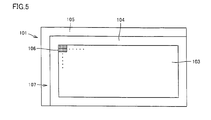
- Fig. 5 is a plan view of liquid crystal display panel 101.
- liquid crystal display panel 101 includes a pixel array region 107 including a display region 103 and a non-display region 104, and a peripheral region 105 located outside of this pixel array region 107.
- Display region 103 serves as a region displaying an image and is formed of a plurality of pixels.
- Non-display region 104 does not display an image and is disposed around display region 103.
- Fig. 6 is a circuit diagram showing a thin film transistor array formed in an active matrix substrate 130.
- Active matrix substrate 130 is provided with a transparent substrate 123 including pixel array region 107 and peripheral region 105 located outside of pixel array region 107.
- a plurality of thin film transistors (switching elements) 115 are arranged in a portion of the main surface of transparent substrate 123 in which display region 103 of pixel array region 107 is located.
- a plurality of gate lines 111 each connected to the gate electrode of thin film transistor 115 and a plurality of source lines 113 each connected to the source electrode of thin film transistor 115 are formed in active matrix substrate 130.
- a pixel electrode 116 is connected to the drain electrode of thin film transistor 115.
- Active matrix substrate 130 is generally formed in a rectangular shape.
- Gate lines 111 extend in the direction of a longer dimension of active matrix substrate 130, and are disposed spaced apart from each other in the direction of a shorter dimension of active matrix substrate 130.
- Source lines 113 extend in the direction of the shorter dimension of active matrix substrate 130 and are disposed spaced apart from each other in the direction of the longer dimension of active matrix substrate 130.
- One pixel electrode 116 is disposed within the region surrounded by gate line 111 and source line 113.
- Gate line 111 extends from thin film transistor 115 through pixel array region 107 to peripheral region 105. Also, a gate pad 112 is formed in a portion of gate line 111 located on peripheral region 105.
- Source line 113 extends from thin film transistor 115 through pixel array region 107 to peripheral region 105. Also, a source pad 114 is formed in a portion of source line 113 located on peripheral region 105.
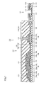
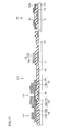
- Fig. 7 is a cross sectional view of active matrix substrate 130.
- Fig. 7 shows a cross sectional view in display region 103 on the left side of the figure and also shows a cross sectional view of gate pad 112 formed in peripheral region 105 on the right side of the figure.
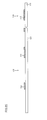
- Fig. 8 is a cross sectional view of source pad 114 formed in peripheral region 105.
- Fig. 9 is a schematic plan view partially showing the inside of pixel array region 107.
- active matrix substrate 130 includes transparent substrate 123 on which thin film transistor 115 is formed.
- Active matrix substrate 130 includes a gate electrode 132 located within pixel array region 107 and formed on transparent substrate 123, gate line 111 formed on transparent substrate 123 and connected to gate electrode 132, gate pad 112 located in peripheral region 105 and formed on transparent substrate 123, and gate insulating film 133 formed so as to cover gate electrode 132, gate line 111 and gate pad 112.
- Gate electrode 132, gate line 111 and gate pad 112 are integrally formed as shown in Fig. 9 .
- Gate line 111 connects gate electrode 132 and gate pad 112 while gate pad 112 is formed at the end of gate line 111.
- active matrix substrate 130 includes a semiconductor layer 134 formed on the upper surface of gate insulating film 133 and located above gate electrode 132. a drain electrode (first electrode) 136 formed on this semiconductor layer 134, and a source electrode 135 5 formed on semiconductor layer 134 and spaced apart from drain electrode 136.
- Thin film transistor 115 includes gate electrode 132, semiconductor layer 134, and source electrode 135 and drain electrode 136.
- Semiconductor layer 134 includes an amorphous silicon film (a-Si film: i layer) 134a formed on gate insulating film 133, and an amorphous silicon film (n+ layer) 134b formed on this amorphous silicon film (i layer) 134a.
- Amorphous silicon film (i layer) 134a functions as a channel portion of thin film transistor 115.
- drain electrode 136 has a drain line 117 connected thereto, and this drain line 117 is connected to a drain pad portion 118.
- Pixel electrode 116 is connected to this drain pad portion 118.
- Drain electrode 136, drain line 117 and drain pad portion 118 are integrally formed, in which drain electrode 136 and pixel electrode 116 are electrically connected to each other.
- Pixel electrode 116 is formed of an ITO film.
- Source line 113 is connected to source electrode 135.
- Source line 113 also has an end to which source pad 114 is connected via a contact 125.
- Source electrode 135 and source line 113 are formed on gate insulating film 133 while source pad 114 is formed on the main surface of transparent substrate 123.
- Contact 125 shown in Fig. 9 is formed so as to pass through gate insulating film 133, and connects the end of source pad 114 and the end of source line 113.
- Gate electrode 132, gate line 111, gate pad 112, and source pad 114 each are formed on the main surface of transparent substrate 123, and made of the same first aluminum alloy material film.
- Drain electrode 136, drain line 117, drain pad portion 118, source electrode 135, and source line 113 include their respective second aluminum alloy material films 136b, 135b, and their respective metal films 136a, 135a formed below these aluminum alloy material films 136a, 135b.
- the first aluminum alloy material film includes aluminum as a base material, an alloy component (first alloy component) containing at least one type of element selected from the group consisting of cobalt (Co), rhodium (Rh), nickel (Ni), palladium (Pd), carbon (C), silicon (Si), germanium (Ge), and tin (Sn), and another component (first another component) containing an element different from aluminum and each element listed above, in which the total number of types of the elements of the alloy component and another component is three or more.
- first alloy component containing at least one type of element selected from the group consisting of cobalt (Co), rhodium (Rh), nickel (Ni), palladium (Pd), carbon (C), silicon (Si), germanium (Ge), and tin (Sn)
- another component first another component containing an element different from aluminum and each element listed above, in which the total number of types of the elements of the alloy component and another component is three or more.
- Second aluminum alloy material films 135b and 136b each also include aluminum as a base material, an alloy component (second alloy component) containing at least one type of element selected from the group consisting of cobalt (Co), rhodium (Rh), nickel (Ni), palladium (Pd), carbon (C), silicon (Si), germanium (Ge), and tin (Sn), and another component (second another component) containing an element different from aluminum and each element listed above, in which the total number of types of the elements of the alloy component and another component is three or more.
- an alloy component containing at least one type of element selected from the group consisting of cobalt (Co), rhodium (Rh), nickel (Ni), palladium (Pd), carbon (C), silicon (Si), germanium (Ge), and tin (Sn)
- another component second another component containing an element different from aluminum and each element listed above, in which the total number of types of the elements of the alloy component and another component is three or more.
- the first aluminum alloy material film and second aluminum alloy material films 135b, 136b each can be patterned by wet etching and also can suppress generation of dust when forming each line, pad and electrode, so that excellent patterning can be carried out. This allows improvement in the yield of active matrix substrate 130, liquid crystal display device 300, and the like.
- the first aluminum alloy material film and second aluminum alloy material films 135b, 136b each include an alloy component containing at least one type of element selected from the group consisting of cobalt (Co), rhodium (Rh), nickel (Ni), palladium (Pd), carbon (C), silicon (Si), germanium (Ge), and tin (Sn), thereby allowing improvement in contact resistance with the transparent conductive film such as an ITO film.
- the sheet resistance can be reduced and the resistance to chemical solution can be enhanced.
- Examples of another component may include copper (Cu), lanthanum (La), boron (B), neodymium (Nd), silver (Ag), gold (Au), platinum (Pt), yttrium (Y), niobium (Nb), tungsten (W), and zirconium (Zr).
- pixel electrode 116 is connected to aluminum alloy material film 136b of drain pad portion 118.
- the potential difference between the above-described aluminum alloy material film and the ITO film is approximately 1.0V while the potential difference between aluminum and the ITO film is approximately 1.6V. Accordingly, when comparing the case where the aluminum alloy material film and the ITO film are in contact with each other with the case where aluminum and the ITO film are in contact with each other, the aluminum alloy material film is less likely to corrode. Therefore, pixel electrode 116 and the aluminum alloy material film can be directly connected, as shown also in Fig. 7 . Similarly, gate pad 112 formed of an aluminum alloy material film and an ITO film (transparent conductive film) 141 can also be brought into direct contact with each other.
- Fig. 10 is a cross sectional view schematically showing a portion in which aluminum alloy material film 136b and pixel electrode 116 are in contact with each other.
- aluminum alloy material film 136b includes a base material 119b and a plurality of precipitates 119a.
- Precipitates 119a are conductive granular precipitates. Precipitates 119a are distributed from the inside of base material 119b over the surface thereof. Also, precipitates 119a are exposed from the surface of base material 119b in a portion of the surface of second aluminum alloy material film 136b that is in contact with pixel electrode 116.
- a precipitate is represented as Al x R y (X and Y each are a positive integer: R is one of elements including cobalt, rhodium, nickel, palladium, carbon, silicon, germanium, and tin).
- precipitate 119a is Al 3 Ni.
- the alloy component containing at least one type selected from the group consisting of cobalt, rhodium, nickel, palladium, carbon, silicon, germanium, and tin that are included in second aluminum alloy material films 135b and 136b is 0.5 wt% or more.
- the alloy component it becomes possible to ensure the resistance to developing solution at the time when second aluminum alloy material films 135b and 136b and the ITO film are stacked, and also possible to suppress occurrence of corrosion in second aluminum alloy material films 135b and 136b.
- the contact resistance between second aluminum alloy material films 135b, 136b and the ITO film can also be suppressed.
- the alloy component containing at least one type of element selected from the group consisting of cobalt, rhodium, nickel, palladium, carbon, silicon, germanium, and tin is 4.5 wt% or less.
- An example of the aluminum alloy material film may be an Al-Ni-Cu-La alloy material film containing aluminum (Al) as a base material, nickel (Ni) as an alloy component, and copper (Cu) and lanthanum (La) as another components.
- Another example may be an Al-Ni-Ge-Nd alloy material film containing aluminum (Al) as a base material, nickel (Ni) and germanium (Ge) as alloy materials, and neodymium (Nd) as another component.
- Al aluminum
- Ni nickel
- Ge germanium
- Nd neodymium
- Another example may be an Al-Co-Ge-Nd alloy material film containing aluminum (Al) as a base material, cobalt (Co) and germanium (Ge) as alloy components, and neodymium (Nd) as another component.
- Al aluminum
- Co cobalt
- Ge germanium
- Nd neodymium
- the aluminum alloy material film may be an Al-Ni-B alloy material film containing aluminum (Al) as a base material, nickel (Ni) as an alloy component, and boron (B) as another component.
- the above-described aluminum alloy material film includes aluminum as a base material, an alloy component containing at least one type of element selected from the group consisting of cobalt (Co), rhodium (Rh), nickel (Ni), palladium (Pd), carbon (C), silicon (Si), germanium (Ge), and tin (Sn), and another component containing an element different from aluminum and each element listed above.
- an "element different from aluminum and each element listed above” is copper (Cu), lanthanum (La), boron (B), neodymium (Nd), silver (Ag), gold (Au), platinum (Pt), yttrium (Y), niobium (Nb), tungsten (W), and zirconium (Zr).
- Cu copper
- La lanthanum
- B boron
- Nd neodymium
- silver Ag
- gold Au
- Y yttrium
- Nb niobium
- W tungsten
- Cu copper
- La lanthanum
- B boron
- Nd neodymium
- the Al-Ni-Cu-La alloy material film, the Al-Ni-Ge-Nd alloy material film and the Al-Co-Ge-Nd alloy material film among the above-described aluminum alloy material films each include aluminum as a base material, an alloy component containing at least one type of element selected from the group consisting of cobalt, rhodium, nickel, palladium, carbon, silicon, germanium, and tin, and another component containing an element different from aluminum and each element listed above, in which the total number of types of the elements of the alloy component and another component is three or more.
- nickel (Ni) is selected, for example, from the group consisting of cobalt, rhodium, nickel, palladium, carbon, silicon, germanium, and tin.
- the aluminum alloy material film made of 1.0 wt% of nickel, 0.5 wt% of copper (Cu), 0.3 wt% of lanthanum (La), and aluminum (Al) can be employed as second aluminum alloy material films 135b and 136b.
- nickel is preferable to employ nickel as an alloy component.
- Metal films 135a and 136a are formed on the lower surfaces of second aluminum alloy material films 135b and 136b, respectively, and formed between their respective second aluminum alloy material films 135b and 136b and semiconductor layer 134.
- Metal films 135a and 136a each are formed of elements greater in density than the element of each synthetic metal of second aluminum alloy material films 135b and 136b and than the element of another component different from aluminum and cobalt, rhodium, nickel, palladium, carbon, silicon, germanium, and tin.
- Metal films 135a and 136a are formed of molybdenum (Mo), for example. These metal films 135a and 136a suppress the alloy components contained in second aluminum alloy material films 135b and 136b from reaching semiconductor layer 134 and being distributed into semiconductor layer 134, and also suppress variation in the Vth value and the like of thin film transistor 115.
- Mo molybdenum
- active matrix substrate 130 includes ITO film 141 formed on the upper surface of gate pad 112, in which gate pad 112 is in direct contact with ITO film 141.
- Fig. 11 is a cross sectional view showing the details of a portion in which ITO film 141 and gate pad 112 are in contact with each other.
- gate pad 112 includes a base material 129b and a plurality of precipitates 129a.
- Precipitates 129a are conductive granular precipitates. Precipitates 129a are distributed from the inside of base material 129b over the surface of base material 129b.
- precipitates 129a are exposed in a portion of the surface of gate pad 112 that is in contact with ITO film 141. Precipitates 129a and ITO film 141 are in contact with each other, thereby allowing reduction in the contact resistance between ITO film 141 and gate pad 112.
- the alloy component containing at least one type selected from the group consisting of cobalt, rhodium, nickel, palladium, carbon, silicon, germanium, and tin contained in gate pad 112 is 0.5 wt% or more.
- the alloy component containing at least one type of element selected from the group consisting of cobalt, rhodium, nickel, palladium, carbon, silicon, germanium, and tin is 0.5 wt% or more and 4.5 wt% or less.
- nickel is selected, for example, from the group consisting of cobalt, rhodium, nickel, palladium, carbon, silicon, germanium, and tin.
- the aluminum alloy formed of 1.0 wt% of nickel (Ni), 0.5 wt% of copper (Cu), 0.3 wt% of lanthanum (La), and aluminum (Al) can be employed as gate pad 112.
- nickel is employed as an alloy component of the aluminum alloy material while copper and lanthanum are employed as another component.
- the distribution density of precipitates 129a formed within the first aluminum alloy material film forming gate pad 112 and source pad 114 is higher than the distribution density of precipitates 119a formed within second aluminum alloy material film 136b.
- the area of precipitates 129a exposed from base material 129b per unit area in the interface between ITO film 141 and gate pad 112 is greater than the area of precipitates 119a exposed from base material 119b per unit area in the interface between pixel electrode 116 and second aluminum alloy material film 136b.
- active matrix substrate 130 includes an interlayer insulating film 140 formed so as to cover source electrode 135, drain electrode 136 and drain pad portion 118.
- Interlayer insulating film 140 includes a passivation film 137 formed on gate insulating film 133 so as to cover source electrode 135, drain electrode 136 and drain pad portion 118, and a planarizing film 138 formed on this passivation film 137.
- Passivation film 137 is formed of a silicon nitride film and, for example, formed at about 250 degrees by the CVD method.
- passivation film 137 and gate insulating film 133 each are formed of a silicon nitride film, in which case the tissue of gate insulating film 133 is more finely structured than that of passivation film 137.
- Planarizing film 138 is formed of organic material such as an acrylic-based synthetic resin.
- Interlayer insulating film 140 is provided with a contact hole 175 formed so as to reach drain pad portion 118.
- Pixel electrode 116 is formed so as to extend from above the upper surface of planarizing film 138 along the inner peripheral surface of contact hole 175 to reach the upper surface of aluminum alloy material film 136b.
- Active matrix substrate 130 includes gate pad 112 formed in peripheral region 105 and ITO film 141 formed on the upper surface of this gate pad 112.
- Gate insulating film 133 and an amorphous silicon film (i layer) 134a formed on this gate insulating film 133 are formed in the surrounding area of gate pad 112.
- Gate insulating film 133 and amorphous silicon film (i layer) 134a each are provided with a contact hole 170 that reaches the upper surface of gate pad 112.
- ITO film 141 is formed so as to extend from the upper surface of amorphous silicon film (i layer) 134a along the inner peripheral surface of contact hole 170 to reach the upper surface of gate pad 112.
- gate insulating film 133 and amorphous silicon film (i layer) 134a formed on this gate insulating film 133 are formed in the surrounding area of source pad 114.
- Gate insulating film 133 and amorphous silicon film (i layer) 134a each are provided with a contact hole 176 that reaches the upper surface of source pad 114.
- ITO film 141 is formed so as to extend from the upper surface of amorphous silicon film (i layer) 134a along the inner peripheral surface of contact hole 176 to reach the upper surface of source pad 114.
- Fig. 12 is a cross sectional view showing the first manufacturing process of the processes of manufacturing liquid crystal display device 300.
- Fig. 13 is a cross sectional view of the region having source pad 114 formed therein, in the first manufacturing process of the processes of manufacturing liquid crystal display device 300 shown in Fig. 12 .
- an aluminum alloy material film is formed on the main surface of transparent substrate 123, for example, using the sputtering vapor deposition method.
- the formed aluminum alloy material film is patterned to form gate electrode 132, gate line 111, gate pad 112, and source pad 114 on the main surface of transparent substrate 123.
- the aluminum alloy material film can be patterned by wet etching, so that gate line 111, gate pad 112, gate electrode 132, and source pad 114 can be excellently formed.
- gate line 111, gate pad 112, gate electrode 132, and source pad 114 each have a thickness of about 2000 ⁇ , for example.
- Fig. 14 is a cross sectional view showing the manufacturing process after the process of manufacturing liquid crystal display device 300 shown in Figs. 12 and 13 described above.
- Fig. 15 is a cross sectional view of source pad 114 in the manufacturing process shown in Fig. 14 .
- gate insulating film 133 is formed on the main surface of transparent substrate 123 so as to cover gate electrode 132, gate line 111, gate pad 112, and source pad 114.
- Gate insulating film 133 is, for example, formed by the CVD method, in which case the film forming temperature is approximately 350 °C, for example.
- gate insulating film 133 When forming gate insulating film 133, the temperature within the chamber is increased, thereby increasing the temperature of each of gate electrode 132, gate line 111, gate pad 112, and source pad 114 which are already formed therein. Then, gate electrode 132, gate line 111, gate pad 112, and source pad 114 are cooled, thereby causing conductive precipitates to settle within gate electrode 132, gate line 111, gate pad 112, and source pad 114.
- the precipitate is represented as Al x R y (X and Y each are a positive integer: R is one of Co, Rh, Ni, Pd, C, Si, Ge and Sn).
- gate insulating film 133 is formed of a silicon nitride film and has a film thickness of approximately 4100 ⁇ , for example.
- gate insulating film 133 After forming gate insulating film 133, an amorphous silicon film (i layer) and an amorphous silicon film (n+ layer) are sequentially formed on the upper surface of gate insulating film 133 by the CVD method. Then, the amorphous silicon film (i layer) and the amorphous silicon film (n+ layer) are patterned. Consequently, semiconductor layer 134 including amorphous silicon film (i layer) 134a and an amorphous silicon film (n+ layer) 134b is formed.
- Amorphous silicon film (i layer) 134a has a film thickness of ; for example, about 1750 ⁇ while amorphous silicon film (n+ layer) 134b has a film thickness of, for example, about 550 ⁇ .
- Amorphous silicon film (i layer) 134a remains in each portion of the upper surface of gate insulating film 133 that is located above gate electrode 132 and located above gate pad 112.
- Amorphous silicon film (i layer) 134a formed above gate electrode 132 is patterned so as to cover gate electrode 132. On the upper surface of this amorphous silicon film (i layer) 134a, amorphous silicon film (n+ layer) 134b is formed spaced apart therefrom.
- Amorphous silicon film (i layer) 134a formed above gate pad 112 is provided with a hole 134f.
- Amorphous silicon film (n+ layer) 134b is formed on the upper surface of amorphous silicon film (i layer) 134a formed above this gate pad 112. This amorphous silicon film (n+ layer) 134b is also provided with a hole 134e in communication with hole 134f.
- gate insulating film 133 located above gate pad 112 is exposed through hole 134e and hole 134f to the outside.
- Amorphous silicon film (i layer) 134a formed above source pad 114 is provided with a hole 134h.
- Amorphous silicon film (n+ layer) 134b is formed on the upper surface of amorphous silicon film (i layer) 134a formed above this source pad 114.
- This amorphous silicon film (n+ layer) 134b is also provided with a hole 134g in communication with hole 134h.
- gate insulating film 133 located above source pad 114 is exposed through hole 134h and hole 134g to the outside.
- Fig. 16 is a plan view during the manufacturing process shown in Figs. 14 and 15 described above.
- a plurality of gate lines 111 extending in one direction are formed spaced apart from each other on the main surface of transparent substrate 123.
- gate pad 112 is formed at the end of each gate line 111.
- a plurality of source pads 114 are formed on the main surface of transparent substrate 123 that are spaced apart from each other in the direction in which gate lines 111 extend.
- Fig. 17 is a cross sectional view showing the manufacturing process after the process of manufacturing liquid crystal display device 300 shown in Figs. 14 to 16 described above.
- Fig. 18 is a cross sectional view of source pad 114 during the manufacturing process shown in Fig. 17 .
- metal film 136a formed of molybdenum (Mo) and second aluminum alloy material film 136b are sequentially formed.
- metal film 135a and second aluminum alloy material film 136b are patterned using a mask.
- metal film 135a and second aluminum alloy material film 136b can be patterned by wet etching while source electrode 135 and drain electrode 136 can be excellently patterned.
- amorphous silicon film (n+ layer) 134b located on gate electrode 132 and source pad 114 are also removed.
- Fig. 19 is a plan view during the manufacturing process shown in Figs. 17 and 18 . As shown in this Fig. 19 , metal film 135a and second aluminum alloy material film 136b are patterned to thereby form source line 113, drain pad portion 118, drain line 117, drain electrode 136, and source electrode 135.
- a contact hole 125a is formed at the end of source line 113 located above the end of first aluminum alloy material film forming source pad 114.
- This contact hole 125a passes through gate insulating film 133 located between source line 113 and source pad 114. Consequently, the upper surface of the first aluminum alloy material film forming source pad 114 is exposed from the bottom of contact hole 125a.
- Fig. 20 is a cross sectional view showing the manufacturing process after the manufacturing process shown in Figs. 17 to 19 described above.
- Fig. 21 is a cross sectional view of source pad 114 during the manufacturing process shown in Fig. 20 .
- passivation film 137 serving as a silicon nitride film is first formed using the CVD method.
- the film forming temperature in this case is approximately 250 degrees, for example.
- Passivation film 137 is formed so as to cover second aluminum alloy material films 135b, 136b and gate insulating film 133.
- Second aluminum alloy material film 135b is also heated by the heat at the time when passivation film 137 is formed. This leads to formation of precipitates within second aluminum alloy material film 135b.
- the film forming temperature of passivation film 137 is lower than the film forming temperature of gate insulating film 133. Accordingly, the precipitation density of the precipitates settling within second aluminum alloy material films 135b, 136b is lower than the precipitation density of the precipitates settling within the first aluminum alloy material film forming gate line 111 and the like. In addition, the precipitation density indicates a volume of the precipitates settling in a unit volume.
- planarizing film 138 is formed.
- Planarizing film 138 is formed of an acrylic-based organic material, for example. This planarizing film 138 is patterned to remove the portion located on peripheral region 105. Consequently, planarizing film 138 located on source pad 114 and gate pad 112 is removed. Furthermore, during this patterning, planarizing film 138 is patterned to provide a contact hole.
- This patterned planarizing film 138 is used as a mask to pattern passivation film 137 and the like.
- passivation film 137 located on drain pad portion 118 is patterned to expose a part of the upper surface of drain pad portion 118, as shown in Fig. 20 .
- gate insulating film 133 is patterned using amorphous silicon film (i layer) 134a as a mask, to form contact hole 170.
- gate insulating film 133 formed on source pad 114 is patterned using amorphous silicon film (i layer) 134a as a mask. Consequently, contact hole 176 is formed to expose a part of the upper surface of source pad 114.
- gate insulating film 133 and passivation film 137 each are formed of a silicon nitride film.
- This surface treatment causes the precipitates to be exposed from the upper surface of each of second aluminum alloy material film 135b, source pad 114 and gate pad 112.
- Fig. 22 is a plan view during the manufacturing process shown in Figs. 20 and 21 described above. As shown in this Fig. 22 , the end of source pad 114 on the display region 103 side is covered by planarizing film 138 and passivation film 137.
- planarizing film 138 and passivation film 137 are provided with contact hole 125a that reaches the end of source pad 114.
- an ITO film is formed on planarizing film 138 and amorphous silicon film (i layer) 134a. Then, this ITO film is patterned to form pixel electrode 116, ITO film 141 and an ITO film (transparent conductive film) 142.
- liquid crystal display device 300 of the liquid crystal display device according to the present embodiment can be manufactured.
- Liquid crystal display device 300 according to the second embodiment of the present invention will be hereinafter described with reference to Figs. 23 to 32 .
- Any of the configurations shown in Figs. 23 to 32 that are identical or correspond to those shown in Figs. 1 to 22 are designated by the same reference characters and description thereof not be repeated.
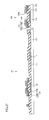
- Fig. 23 is a cross sectional view of active matrix substrate 130 of the liquid crystal display device according to the present second embodiment.
- Fig. 24 is a cross sectional view of source pad 114.
- source electrode 135 is formed on semiconductor layer 134 and gate insulating film 133, and includes a metal film 135a formed of molybdenum (Mo), a metal film (intermediate film) 135e formed on metal film 135a and formed of aluminum (Al), and second aluminum alloy material film 135b formed on this metal film 135e.
- Mo molybdenum
- Al aluminum
- drain electrode 136 includes metal film 136a formed on semiconductor layer 134 and gate insulating film 133, a metal film 136e formed on the upper surface of this metal film 136a, and second aluminum alloy material film 136b formed on the upper surface of this metal film 136e.
- source electrode 135, drain electrode 136, drain pad portion 118 and the like each include a metal film that is formed of Al and disposed between the aluminum alloy material film and the metal film functioning as a diffusion preventing film.
- the electrical resistance can be reduced while the manufacturing cost can be lowered.
- Fig. 25 is a cross sectional view showing the first manufacturing process of the processes of manufacturing liquid crystal display device 300 according to the third embodiment of the present invention.
- Fig. 26 is a cross sectional view in the region having source pad 114 formed therein.
- the first aluminum metal material film is formed and patterned by wet etching, thereby forming gate electrode 132, gate line 111, gate pad 112, and source pad 114.
- Fig. 27 is a cross sectional view showing the manufacturing process after the manufacturing process shown in Figs. 25 and 26 described above.
- Fig. 28 is a cross sectional view in the region having source pad 114 formed therein.
- semiconductor layer 134 is formed on each of gate electrode 132, gate pad 112 and source pad 114.
- Fig. 29 is a cross sectional view showing the manufacturing process after the manufacturing process shown in Figs. 27 and 28 described above.
- Fig. 30 is a cross sectional view in the region having source pad 114 formed therein during the manufacturing process shown in Fig. 29 .
- the metal film formed of molybdenum (Mo), the metal film formed of aluminum (Al), and the above-described second aluminum alloy material film are sequentially formed. Then, these stacked metal films are patterned by wet etching, to form source electrode 135, drain electrode 136 and drain pad portion 118.
- Fig. 31 is a cross sectional view showing the manufacturing process after the manufacturing process shown in Figs. 29 and 30 .
- Fig. 32 is a cross sectional view in the region having source pad 114.formed therein during the manufacturing process shown in Fig. 31 .
- planarizing film 138 and passivation film 137 are formed.
- an ITO film is formed on planarizing film 138 and then patterned to form pixel electrode 116 and the like.
- Liquid crystal display device 300 according to the third embodiment of the present invention will be hereinafter described with reference to Figs 33 to 44 .
- any of the configurations shown in Figs. 33 to 44 that are identical or correspond to those shown in Figs. 1 to 32 described above will be designated by the same reference characters, and description thereof will not be repeated.
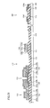
- Fig. 33 is a cross sectional view showing the liquid crystal display device according to the third embodiment of the present invention.
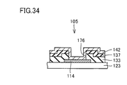
- Fig. 34 is a cross sectional view of source pad 114.
- pixel electrode 116 is formed on the upper surface of passivation film 137. Furthermore, gate insulating film 133 is formed in the peripheral edge of gate pad 112, and passivation film 137 is formed on this gate insulating film 133. Also, gate insulating film 133 and passivation film 137 are provided with contact hole 170 through which a part of the upper surface of gate pad 112 is exposed.
- ITO film (transparent conductive film) 141 is formed to extend from the upper surface of passivation film 137 along the inner peripheral surface of contact hole 170 to reach the upper surface of gate pad 112.
- gate insulating film 133 is formed in the peripheral edge of source pad 114, and passivation film 137 is formed on the upper surface of this gate insulating film 133. Furthermore, gate insulating film 133 and passivation film 137 are provided with contact hole 176 passing through gate insulating film 133 and passivation film 137 and reaching the upper surface of source pad 114. Furthermore, ITO film 142 is formed to extend from the upper surface of passivation film 137 along the inner peripheral surface of contact hole 176 to reach the upper surface of source pad 114.
- planarizing film 138 is not formed, but pixel electrode 116 and ITO films 141, 142 are formed on passivation film 137.
- gate line 111, gate pad 112 and source pad 114 are formed of the first aluminum alloy material film as in the above-described first and second embodiments.
- second aluminum alloy material films 136b and 135b each are also formed of the aluminum alloy material similar to that in the above-described first and second embodiments.
- liquid crystal display device 300 configured as set forth above will be hereinafter described with reference to Figs. 35 to 44 .
- Fig. 35 is a cross sectional view showing the first manufacturing process of the processes of manufacturing liquid crystal display device 300 according to the present third embodiment.
- Fig. 36 is a cross sectional view of the region having a source pad formed therein during the manufacturing process shown in Fig. 35 described above.
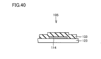
- an aluminum alloy material film is formed on the main surface of transparent substrate 123, and then patterned by wet etching. Consequently, gate line 111, gate pad 112, source pad 114, and gate electrode 132 are formed on the main surface of transparent substrate 123.
- gate insulating film 133 is formed on the main surface of transparent substrate 123 so as to cover gate line 111, gate pad 112, source pad 114, and gate electrode 132. Then, amorphous silicon film (i layer) 134a and amorphous silicon film (n+ layer) 134b are stacked, which are then subjected to patterning.
- amorphous silicon film (i layer) 134a and amorphous silicon film (n+ layer) 134b located above gate pad 112 and source pad 114 are removed.
- the metal film formed of molybdenum (Mo), the metal film formed of aluminum (Al), and the above-described second aluminum alloy material film are sequentially formed. Then, these stacked metal films are patterned by wet etching. Consequently, each of the metal films located above gate pad 112 and source pad 114 is removed.
- drain pad 118, drain electrode 136 and source electrode 135 are formed.
- passivation film 137 is formed.
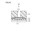
- a resist film 157 is formed on this passivation film 137.
- Resist film 157 is then patterned to form holes 157a, 157b and 157c.
- Hole 157a is located above drain pad 118 while hole 157b is located above gate pad 112.
- hole 157c is located above source pad 114.
- passivation film 137 and gate insulating film 133 are patterned by using, as a mask, resist film 157 having each hole formed therein.
- surface treatment is applied using an alkaline solution to the upper surface of second aluminum alloy material film 136b, the upper surface of gate pad 112 and the upper surface of source pad 114.
- liquid crystal display device 300 according to the present third embodiment can be manufactured.
- liquid crystal display device 300 having thin film transistor 115 including an amorphous silicon (a-Si) film the present invention is not limited thereto.
- the present invention is also applicable to liquid crystal display device 300 employing a low-temperature polysilicon TFT using low temperature polysilicon (p-Si).
- an oxide semiconductor may be employed in place of thin film transistor 115.
- Table I described below shows the results of evaluation about the resistance to the developing solution for a stack of the ITO film and the aluminum alloy material film (the aluminum alloy material film on the ITO film) that has varied wt% of alloy component containing at least one type selected from the group consisting of Co, Rh, Ni, Pd, C, Si, Ge, and Sn.
- alloy component containing at least one type selected from the group consisting of Co, Rh, Ni, Pd, C, Si, Ge, and Sn.
- “B” means that corrosion occurred
- A means that corrosion did not occur.
- Table 2 described below shows a graph about the evaluation of the contact resistance for a stack of the aluminum alloy material film and the ITO film.
- “A” means that the contact resistance is 100 ⁇ or less. It is to be noted that the contact resistance between pure aluminum and the ITO film is 100 ⁇ .
- the resistance to developing solution can be ensured in the case where the alloy component containing at least one type selected from the group consisting of Co, Rh, Ni, Pd, C, Si, Ge, and Sn is 0.5 wt% or more. Furthermore, it is also recognized that the resistance to developing solution can be ensured by employing the aluminum alloy material film including 0.5 wt% or more and 4.5 wt% or less of the alloy component containing at least one type selected from the group consisting of Co, Rh, Ni, Pd, C, Si, Ge, and Sn.
- the contact resistance can be suppressed as compared with the case where pure aluminum is employed.
- the contact resistance can be suppressed as compared with the case where pure aluminum is employed.
- the resistance to developing solution can be ensured while the contact resistance can be reduced by employing the aluminum alloy material film including 0.5 wt% or more and 4.5 wt% or less of the alloy component containing at least one type selected from the group consisting of Co, Rh, Ni, Pd, C, Si, Ge, and Sn.
- Table 3 described below shows the components of second aluminum alloy material film 135b.
- Table 4 described below also shows the results of determination as to whether Ni of second aluminum alloy material film 135b is diffused into semiconductor layer 134 located below metal film 135a in the case where metal film 135a is formed on the lower surface of second aluminum alloy material film 135b shown in Table 3.
- Table 4 shows the results of determination as to whether Ni of second aluminum alloy material film 135b is diffused into semiconductor layer 134 in the case where metal film 135a is formed of titanium (Ti) and the case where metal film 135a is formed of molybdenum (Mo).
- metal film 135a is formed of titanium while diffusion of "Ni” could not be confirmed in the case where metal film 135a was formed of molybdenum.
- metal film 135a is formed of molybdenum, thereby allowing diffusion of "Ni” to be suppressed and also allowing the performance of the thin film transistor to be ensured.
- the density of titanium (Ti) is 4.54 which is smaller than the density of each of elements Ni, Cu and La constituting a part of second aluminum alloy material film 135b.
- molybdenum (Mo) is greater in density than any of the elements constituting second aluminum alloy material film 135b.
- the inventors compared the case where an aluminum alloy material film was formed on the titanium (Ti) film with the case where the above-described aluminum alloy material film was formed on the Mo film. As a result of earnest effort of study by the inventors, it was found that Ni was diffused into the titanium (Ti) film at a content ratio of 40% in the aluminum alloy material film. In contrast, the example in which the above-described aluminum alloy material film was formed on the molybdenum (Mo) film showed that Ni was diffused into the molybdenum film at a content ratio of 1.0% or less in the aluminum alloy material film.
- SIMS Secondary Ion Mass Spectrometry
- the present invention can be applied to a liquid crystal display device and a method of manufacturing the liquid crystal display device.
Landscapes
- Physics & Mathematics (AREA)
- Nonlinear Science (AREA)
- Chemical & Material Sciences (AREA)
- Optics & Photonics (AREA)
- Crystallography & Structural Chemistry (AREA)
- Mathematical Physics (AREA)
- General Physics & Mathematics (AREA)
- Engineering & Computer Science (AREA)
- Mechanical Engineering (AREA)
- Materials Engineering (AREA)
- Microelectronics & Electronic Packaging (AREA)
- Metallurgy (AREA)
- Organic Chemistry (AREA)
- Liquid Crystal (AREA)
- Thin Film Transistor (AREA)
- Electrodes Of Semiconductors (AREA)
- Internal Circuitry In Semiconductor Integrated Circuit Devices (AREA)
- Devices For Indicating Variable Information By Combining Individual Elements (AREA)
Abstract
At least one of a drain electrode (136), a source electrode (135) and a gate electrode (132) includes an aluminum alloy material film. The aluminum alloy material film includes aluminum as a base material, an alloy component containing at least one type of element selected from the group consisting of cobalt, rhodium, nickel, palladium, carbon, silicon, germanium, and tin, and another component containing an element different from aluminum and each element listed above, in which the total number of types of the elements of the alloy component and another component is three or more.
Description
- The present invention relates a liquid crystal display device and a method of manufacturing the liquid crystal display device.
- Various types of liquid crystal display devices have been conventionally proposed. For example, the liquid crystal display device disclosed in Japanese Patent Laying-Open No.
09-197433 - The gate pad includes a metal film formed of aluminum (Al) and the like, and a metal film formed on this metal film and formed of titanium (Ti) and the like. The source electrode and the drain electrode each are also formed of titanium and the like.
- Furthermore, Japanese Patent Laying-Open No.
2004-214606 -
- PTL 1: Japanese Patent Laying-Open No.
09-197433 - PTL 2: Japanese Patent Laying-Open No.
2004-214606 - In the process of manufacturing the above-described conventional liquid crystal display device, it becomes necessary to pattern titanium (Ti) when a gate electrode, a source electrode and a drain electrode are formed.
- When patterning titanium (Ti), plasma dry etching is employed. When titanium (Ti) is patterned by dry etching, fine titanium dust is produced within the chamber.
- When the titanium dust falls onto the substrate, the gate electrode and the like cannot be accurately patterned, leading to a significant decrease in the yield.
- The present invention has been made in light of the above-described problems. An object of the present invention is to provide a liquid crystal display device and a method of manufacturing the liquid crystal display device that allow improvement in the yield.
- A liquid crystal display device according to the present invention includes a substrate including a pixel array region and a peripheral region located outside of the pixel array region; a switching element formed in the pixel array region; an electrode provided in the switching element; a lead line connected to the switching element; and a pad portion connected to the lead line. At least one of the electrode, the lead line and the pad portion includes an aluminum alloy material film. The aluminum alloy material film includes aluminum as a base material, an alloy component containing at least one type of element selected from the group consisting of cobalt, rhodium, nickel, palladium, carbon, silicon, germanium, and tin, and another component containing an element different from aluminum and each element listed above, in which a total number of types of the elements of the alloy component and another component is three or more.
- Preferably, the aluminum alloy material film contains 0.5 wt% or more of the alloy component.
- Preferably, the alloy component contained in the aluminum alloy material film is 4.5 wt% or less. Preferably, the aluminum alloy material film contains a conductive precipitate.
- Preferably, the electrode of the switching element includes a drain electrode and further includes a pixel electrode connected to the drain electrode. The drain electrode includes the aluminum alloy material film. The pixel electrode is connected to the aluminum alloy material film of the drain electrode. The precipitate is exposed in at least a portion of a surface of the aluminum alloy material film that is in contact with the pixel electrode.
- Preferably, the switching element further includes a semiconductor layer. The electrode of the switching element includes a source electrode and a drain electrode formed on the semiconductor layer. The drain electrode and the source electrode each include the aluminum alloy material film and a metal film disposed between the aluminum alloy material film and the semiconductor layer. The metal film is formed of an element greater in density than the element of the alloy component and the element of another component.
- Preferably, the drain electrode and the source electrode each further include an intermediate film formed of aluminum and formed between the aluminum alloy material film and the metal film. Preferably, the metal film is formed of molybdenum.
- Preferably, the pad portion is formed of the aluminum alloy material film. Preferably, a transparent conductive film formed on the pad portion is further included. The pad portion is formed of the aluminum alloy material film. The aluminum alloy material film includes a conductive precipitate. The conductive precipitate is exposed in a portion of a surface of the pad portion that is in contact with the transparent conductive film.
- Preferably, the electrode of the switching element includes a source electrode and a drain electrode. The pad portion is formed of a first aluminum alloy material film. The source electrode and the drain electrode each are formed of a second aluminum alloy material film. The first aluminum alloy material film includes aluminum as a base material, a first alloy component containing at least one type of element selected from the group consisting of cobalt, rhodium, nickel, palladium, carbon, silicon, germanium, and tin, and a first another component containing an element different from aluminum and each element listed above, in which a total number of types of the elements of the first alloy component and the first another component is three or more. The second aluminum alloy material film includes aluminum as a base material, a second alloy component containing at least one type of element selected from the group consisting of cobalt, rhodium, nickel, palladium, carbon, silicon, germanium, and tin, and a second another component containing an element different from aluminum and each element listed above, in which a total number of types of the elements of the second alloy component and the second another component is three or more. The first aluminum alloy material film includes a conductive first precipitate, and the second aluminum alloy material film includes a conductive second precipitate. The first precipitate is greater in distribution density than the second precipitate.
- Preferably, the electrode of the switching element includes a source electrode and a gate electrode. The lead line includes a source line connected to the source electrode and a gate line connected to the gate electrode. The pad portion includes a source pad connected to the source line and a gate pad connected to the gate line. The source pad and the gate pad each are formed of the first aluminum alloy material film.
- Preferably, the switching element includes a gate electrode formed on a main surface of the substrate, a semiconductor layer formed on the gate electrode, a source electrode formed on the semiconductor layer, and a drain electrode formed on the semiconductor layer and spaced apart from the source electrode. The lead line includes a gate line connected to the gate electrode, and a source line connected to the source electrode. The pad portion includes a gate pad connected to the gate line, and a source pad connected to the source line. The gate electrode, the gate line and the gate pad each are formed of the aluminum alloy material film.
- Preferably, the source electrode, the drain electrode and the source pad each include the aluminum alloy material film.
- A liquid crystal display device according to the present invention includes a substrate including a pixel array region and a peripheral region located outside of the pixel array region; a switching element formed in the pixel array region; an electrode provided in the switching element; a lead line connected to the switching element; a pad portion connected to the lead line; and a transparent conductive film formed on the pad portion. At least one of the electrode, the lead line and the pad portion includes an aluminum alloy material film. A potential difference between the aluminum alloy material film and the transparent conductive film is smaller than a potential difference between an aluminum film and the transparent conductive film.
- A liquid crystal display device according to the present invention includes a substrate including a pixel array region and a peripheral region located outside of the pixel array region; a switching element formed in the pixel array region; an electrode provided in the switching element; a lead line connected to the switching element; and a pad portion connected to the lead line. At least one of the electrode, the lead line and the pad portion includes an aluminum alloy material film. The aluminum alloy material film includes aluminum as a base material, an alloy component containing at least one type of element selected from the group consisting of cobalt (Co), rhodium (Rh), nickel (Ni), palladium (Pd), carbon (C), silicon (Si), germanium (Ge), and tin (Sn), and another component containing at least one type of element selected from the group consisting of copper (Cu), a lanthanum (La), boron (B), neodymium (Nd), silver (Ag), gold (Au), platinum (Pt), yttrium (Y), niobium (Nb), tungsten (W), and zirconium (Zr).
- A method of manufacturing a liquid crystal display device according to the present invention provides a method of manufacturing a liquid crystal display device including a substrate including a pixel array region and a peripheral region located outside of the pixel array region; a switching element formed in the pixel array region; an electrode provided in the switching element; a lead line connected to the switching element; a pad portion connected to the lead line. The method includes the steps of: preparing a substrate having a main surface; forming an aluminum alloy material film including aluminum as a base material, an alloy component containing at least one type of element selected from the group consisting of cobalt, rhodium, nickel, palladium, carbon, silicon, germanium, and tin, and another component containing an element different from aluminum and each element listed above, in which a total number of types of the elements of the alloy component and another component is three or more; and patterning the aluminum alloy material film to form at least one of the electrode, the lead line and the pad portion.
- Preferably, the aluminum alloy material film contains 0.5 wt% or more of the alloy component.
- Preferably, the alloy component contained in the aluminum alloy material film is 4.5 wt% or less. Preferably, the electrode is formed by patterning the aluminum alloy material film by wet etching. The method preferably further includes the steps of: heating the aluminum alloy material film to form a precipitate within the aluminum alloy material film; exposing the precipitate on a surface of the aluminum alloy material film; and forming a transparent conductive film in a portion of the surface of the aluminum alloy material film in which the precipitate is exposed.
- Preferably, the step of forming the electrode includes the steps of: forming the aluminum alloy material film on the main surface of the substrate; and patterning the aluminum alloy material film to form a gate electrode, in which case the electrode is the gate electrode.
- Preferably, the method further includes the step of forming a gate insulating film so as to cover the gate electrode. A conductive precipitate is formed within the aluminum alloy material film by heat for forming the gate insulating film.
- Preferably, the method further includes the steps of: forming a gate electrode on the main surface of the substrate; forming a gate insulating film so as to cover the gate electrode; forming a semiconductor layer on the gate insulating film and above the gate electrode; and forming, on the semiconductor layer, a metal film formed of an element greater in density than the element of the alloy component and the element of another component. The step of forming the electrode includes the steps of: forming the aluminum alloy material film on the metal film; and patterning the aluminum alloy material film to form a source electrode and a drain electrode each as the electrode.
- Preferably, the metal film is formed of molybdenum. Preferably, the method further includes the step of forming an insulating film so as to cover the source electrode and the drain electrode, in which a precipitate is formed within the source electrode and the drain electrode by heat for forming the insulating film.
- A method of manufacturing a liquid crystal display device according to the present invention provides a method of manufacturing a liquid crystal display device including a substrate including a pixel array region and a peripheral region located outside of the pixel array region, a switching element formed in the pixel array region, an electrode provided in the switching element, a lead line connected to the switching element, and a pad portion connected to the lead line. The method includes the steps of: preparing a substrate having a main surface; forming an aluminum alloy material film including aluminum as a base material, an alloy component containing at least one type of element selected from the group consisting of cobalt (Co), rhodium (Rh), nickel (Ni), palladium (Pd), carbon (C), silicon (Si), germanium (Ge), and tin (Sn), and another component containing at least one type of element selected from the group consisting of copper (Cu), lanthanum (La), boron (B), neodymium (Nd), silver (Ag), gold (Au), platinum (Pt), yttrium (Y), niobium (Nb), tungsten (W), and zirconium (Zr); and patterning the aluminum alloy material film to form at least one of the electrode, the lead line and the pad portion.
- The liquid crystal display device and the method of manufacturing the liquid crystal display device according to the present invention allow improvement in the yield.
-
-
Fig. 1 is an exploded perspective view showing the configuration of atelevision receiver 500 according to the first embodiment of the present invention. -
Fig. 2 is a perspective view schematically showing a liquidcrystal display device 300. -
Fig. 3 is a plan view schematically showing a liquidcrystal display element 200. -
Fig. 4 is an exploded perspective view showing the state where a liquidcrystal display panel 101 and apolarization plate 156 are arranged. -
Fig. 5 is a plan view of liquidcrystal display panel 101. -
Fig. 6 is a circuit diagram showing a thin film transistor array formed in anactive matrix substrate 130. -
Fig. 7 is a cross sectional view ofactive matrix substrate 130. -
Fig. 8 is a cross sectional view of asource pad 114 formed in aperipheral region 105. -
Fig. 9 is a schematic plan view partially showing the inside of apixel array region 107. -
Fig. 10 is a cross sectional view schematically showing a portion in which an aluminumalloy material film 136b and apixel electrode 116 are in contact with each other. -
Fig. 11 is a cross sectional view showing the details of a portion in which anITO film 141 and agate pad 112 are in contact with each other. -
Fig. 12 is a cross sectional view showing the first manufacturing process of the processes of manufacturing liquidcrystal display device 300. -
Fig. 13 is a cross sectional view of the region having source pad 114 formed therein, in the first manufacturing process of the processes of manufacturing liquidcrystal display device 300 shown inFig. 12 . -
Fig. 14 is a cross sectional view showing the manufacturing process after the processes of manufacturing liquidcrystal display device 300 shown inFigs. 12 and13 . -
Fig. 15 is a cross sectional view ofsource pad 114 in the manufacturing process shown inFig. 14 . -
Fig. 16 is a plan view during the manufacturing process shown inFigs. 14 and15 . -
Fig. 17 is a cross sectional view showing the manufacturing process after the processes of manufacturing liquidcrystal display device 300 shown inFigs. 14 to 16 . -
Fig. 18 is a cross sectional view ofsource pad 114 during the manufacturing process shown inFig. 17 . -
Fig. 19 is a plan view during the manufacturing process shown inFigs. 17 and18 . -
Fig. 20 is a cross sectional view showing the manufacturing process after the manufacturing processes shown inFigs. 17 to 19 . -
Fig. 21 is a cross sectional view ofsource pad 114 during the manufacturing process shown inFig. 20 . -
Fig. 22 is a plan view during the manufacturing process shown inFigs. 20 and21 . -
Fig. 23 is a cross sectional view ofactive matrix substrate 130 of the liquid crystal display device according to the present second embodiment. -
Fig. 24 is a cross sectional view ofsource pad 114. -
Fig. 25 is a cross sectional view showing the first manufacturing process of the processes of manufacturing liquidcrystal display device 300 according to the third embodiment of the present invention. -
Fig. 26 is a cross sectional view in the region having source pad 114 formed therein. -
Fig. 27 is a cross sectional view showing the manufacturing process after the manufacturing process shown inFigs. 25 and26 . -
Fig. 28 is a cross sectional view in the region having source pad 114 formed therein. -
Fig. 29 is a cross sectional view showing the manufacturing process after the manufacturing process shown inFigs. 27 and28 . -
Fig. 30 is a cross sectional view in the region having source pad 114 formed therein during the manufacturing process shown inFig. 29 . -
Fig. 31 is a cross sectional view showing the manufacturing process after the manufacturing process shown inFigs. 29 and30 . -
Fig. 32 is a cross sectional view in the region having source pad 114 formed therein during the manufacturing process shown inFig. 31 . -
Fig. 33 is a cross sectional view of a liquid crystal display device according to the third embodiment of the present invention. -
Fig. 34 is a cross sectional view ofsource pad 114. -
Fig. 35 is a cross sectional view showing the first manufacturing process of the processes of manufacturing liquidcrystal display device 300 according to the present third embodiment. -
Fig. 36 is a cross sectional view of the region having a source pad formed therein during the manufacturing process shown inFig. 35 . -
Fig. 37 is a cross sectional view showing the manufacturing process after the manufacturing process shown inFigs. 35 and36 . -
Fig. 38 is a cross sectional view of the region having a source pad formed therein during the manufacturing process shown inFig. 37 . -
Fig. 39 is a cross sectional view showing the manufacturing process after the manufacturing process shown inFigs. 37 and38 . -
Fig. 40 is a cross sectional view of the region having a source pad formed therein during the manufacturing process shown inFig. 39 . -
Fig. 41 is a cross sectional view showing the manufacturing process after the manufacturing process shown inFigs. 39 and40 . -
Fig. 42 is a cross sectional view of the region having a source pad formed therein during the manufacturing process shown inFig. 41 . -
Fig. 43 is a cross sectional view showing the manufacturing process after the manufacturing process shown inFigs. 41 and42 . -
Fig. 44 is a cross sectional view of the region having a source pad formed therein during the manufacturing process shown inFig. 43 . - A liquid crystal display device and a method of manufacturing a liquid crystal display device according to the embodiments of the present invention will be hereinafter described with reference to
Figs. 1 to 44 . - In the embodiments described below, when the number, the quantity and the like are mentioned, the scope of the present invention is not necessarily limited thereto unless otherwise specified. In the following embodiments, each component is not necessarily essential for the present invention unless otherwise specified. Furthermore, when a plurality of embodiments are provided in the following description, it is originally intended to combine characteristic portions in each embodiment as appropriate, unless otherwise specified.
-
Fig. 1 is an exploded perspective view showing the configuration of atelevision receiver 500 according to the first embodiment of the present invention. As shown in thisFig. 1 ,television receiver 500 includes acasing 181 disposed on the front side, acasing 182 disposed on the back side, a liquidcrystal display device 300 disposed betweencasing 181 andcasing 182, anoperation circuit 184, and a supportingmember 185. - Liquid
crystal display device 300 is surrounded bycasings casings - Casing 181 is provided with an
opening 183, through which the image displayed on liquidcrystal display device 300 can be transmitted to the outside. Casing 182 is provided withoperation circuit 184 for operating liquidcrystal display device 300. Casing 182 is supported by supportingmember 185. -
Fig. 2 is a perspective view schematically showing liquidcrystal display device 300. As shown in thisFig. 2 , liquidcrystal display device 300 includes a liquidcrystal display element 200 having a liquidcrystal display panel 101, apolarization plate 156 attached onto one of the main surfaces of liquidcrystal display panel 101, a polarization plate attached onto the other of the main surfaces of liquidcrystal display panel 101, and a backlight unit 186 applying light to liquidcrystal display panel 101. -
Fig. 3 is a plan view schematically showing liquidcrystal display element 200. As shown in thisFig. 3 , liquidcrystal display element 200 includes liquidcrystal display panel 101, agate driver 152 connected to agate terminal portion 150 of liquidcrystal display panel 101, asource driver 153 connected to a sourceterminal portion 151 of liquidcrystal display panel 101, a printedcircuit board wiring 154 to whichgate driver 152 andsource driver 153 are connected, and adisplay control circuit 155 to which printedcircuit board wiring 154 is connected. -
Fig. 4 is an exploded perspective view showing the state where liquidcrystal display panel 101 andpolarization plate 156 are arranged. As shown in thisFig. 4 , liquidcrystal display panel 101 has main surfaces, one of which has apolarization plate 156a attached thereto, and the other of which has anotherpolarization plate 156b attached thereto. - In addition, the polarization axis direction of
polarization plate 156a is orthogonal to the polarization axis direction ofpolarization plate 156b.Polarization plate 156a is irradiated with light from backlight unit 186 shown inFig. 2 . - Liquid
crystal display panel 101 includes an active matrix substrate, an opposing substrate disposed to face this active matrix substrate and spaced apart from this active matrix substrate, and a liquid crystal layer enclosed between the active matrix substrate and the opposing substrate. -
Fig. 5 is a plan view of liquidcrystal display panel 101. As shown in thisFig. 5 , liquidcrystal display panel 101 includes apixel array region 107 including adisplay region 103 and anon-display region 104, and aperipheral region 105 located outside of thispixel array region 107. -
Display region 103 serves as a region displaying an image and is formed of a plurality of pixels.Non-display region 104 does not display an image and is disposed arounddisplay region 103.Fig. 6 is a circuit diagram showing a thin film transistor array formed in anactive matrix substrate 130. -
Active matrix substrate 130 is provided with atransparent substrate 123 includingpixel array region 107 andperipheral region 105 located outside ofpixel array region 107. - A plurality of thin film transistors (switching elements) 115 are arranged in a portion of the main surface of
transparent substrate 123 in which displayregion 103 ofpixel array region 107 is located. A plurality ofgate lines 111 each connected to the gate electrode ofthin film transistor 115 and a plurality ofsource lines 113 each connected to the source electrode ofthin film transistor 115 are formed inactive matrix substrate 130. Apixel electrode 116 is connected to the drain electrode ofthin film transistor 115. -
Active matrix substrate 130 is generally formed in a rectangular shape.Gate lines 111 extend in the direction of a longer dimension ofactive matrix substrate 130, and are disposed spaced apart from each other in the direction of a shorter dimension ofactive matrix substrate 130.Source lines 113 extend in the direction of the shorter dimension ofactive matrix substrate 130 and are disposed spaced apart from each other in the direction of the longer dimension ofactive matrix substrate 130. - One
pixel electrode 116 is disposed within the region surrounded bygate line 111 andsource line 113. -
Gate line 111 extends fromthin film transistor 115 throughpixel array region 107 toperipheral region 105. Also, agate pad 112 is formed in a portion ofgate line 111 located onperipheral region 105. -
Source line 113 extends fromthin film transistor 115 throughpixel array region 107 toperipheral region 105. Also, asource pad 114 is formed in a portion ofsource line 113 located onperipheral region 105. -
Fig. 7 is a cross sectional view ofactive matrix substrate 130. In addition,Fig. 7 shows a cross sectional view indisplay region 103 on the left side of the figure and also shows a cross sectional view ofgate pad 112 formed inperipheral region 105 on the right side of the figure.Fig. 8 is a cross sectional view ofsource pad 114 formed inperipheral region 105.Fig. 9 is a schematic plan view partially showing the inside ofpixel array region 107. - As shown in
Fig. 7 ,active matrix substrate 130 includestransparent substrate 123 on whichthin film transistor 115 is formed.Active matrix substrate 130 includes agate electrode 132 located withinpixel array region 107 and formed ontransparent substrate 123,gate line 111 formed ontransparent substrate 123 and connected togate electrode 132,gate pad 112 located inperipheral region 105 and formed ontransparent substrate 123, andgate insulating film 133 formed so as to covergate electrode 132,gate line 111 andgate pad 112. -
Gate electrode 132,gate line 111 andgate pad 112 are integrally formed as shown inFig. 9 .Gate line 111 connectsgate electrode 132 andgate pad 112 whilegate pad 112 is formed at the end ofgate line 111. - In
Fig. 7 ,active matrix substrate 130 includes asemiconductor layer 134 formed on the upper surface ofgate insulating film 133 and located abovegate electrode 132. a drain electrode (first electrode) 136 formed on thissemiconductor layer 134, and asource electrode 135 5 formed onsemiconductor layer 134 and spaced apart fromdrain electrode 136. -
Thin film transistor 115 includesgate electrode 132,semiconductor layer 134, andsource electrode 135 anddrain electrode 136. -
Semiconductor layer 134 includes an amorphous silicon film (a-Si film: i layer) 134a formed ongate insulating film 133, and an amorphous silicon film (n+ layer) 134b formed on this amorphous silicon film (i layer) 134a. Amorphous silicon film (i layer) 134a functions as a channel portion ofthin film transistor 115. - As shown in
Fig. 9 ,drain electrode 136 has adrain line 117 connected thereto, and thisdrain line 117 is connected to adrain pad portion 118.Pixel electrode 116 is connected to thisdrain pad portion 118.Drain electrode 136,drain line 117 anddrain pad portion 118 are integrally formed, in which drainelectrode 136 andpixel electrode 116 are electrically connected to each other.Pixel electrode 116 is formed of an ITO film. -
Source line 113 is connected to sourceelectrode 135.Source line 113 also has an end to whichsource pad 114 is connected via acontact 125. -
Source electrode 135 andsource line 113 are formed ongate insulating film 133 whilesource pad 114 is formed on the main surface oftransparent substrate 123. - Contact 125 shown in
Fig. 9 is formed so as to pass throughgate insulating film 133, and connects the end ofsource pad 114 and the end ofsource line 113. -
Gate electrode 132,gate line 111,gate pad 112, andsource pad 114 each are formed on the main surface oftransparent substrate 123, and made of the same first aluminum alloy material film. -
Drain electrode 136,drain line 117,drain pad portion 118,source electrode 135, andsource line 113 include their respective second aluminumalloy material films respective metal films alloy material films - The first aluminum alloy material film includes aluminum as a base material, an alloy component (first alloy component) containing at least one type of element selected from the group consisting of cobalt (Co), rhodium (Rh), nickel (Ni), palladium (Pd), carbon (C), silicon (Si), germanium (Ge), and tin (Sn), and another component (first another component) containing an element different from aluminum and each element listed above, in which the total number of types of the elements of the alloy component and another component is three or more.
- Second aluminum
alloy material films - The first aluminum alloy material film and second aluminum
alloy material films active matrix substrate 130, liquidcrystal display device 300, and the like. - The first aluminum alloy material film and second aluminum
alloy material films - Furthermore, by including another component (the first another component, the second another component) containing an element other than aluminum, cobalt (Co), rhodium (Rh), nickel (Ni), palladium (Pd), carbon (C), silicon (Si), germanium (Ge), and tin (Sn), the sheet resistance can be reduced and the resistance to chemical solution can be enhanced.
- Examples of another component may include copper (Cu), lanthanum (La), boron (B), neodymium (Nd), silver (Ag), gold (Au), platinum (Pt), yttrium (Y), niobium (Nb), tungsten (W), and zirconium (Zr).
- As shown in
Fig. 7 ,pixel electrode 116 is connected to aluminumalloy material film 136b ofdrain pad portion 118. - The potential difference between the above-described aluminum alloy material film and the ITO film is approximately 1.0V while the potential difference between aluminum and the ITO film is approximately 1.6V. Accordingly, when comparing the case where the aluminum alloy material film and the ITO film are in contact with each other with the case where aluminum and the ITO film are in contact with each other, the aluminum alloy material film is less likely to corrode. Therefore,
pixel electrode 116 and the aluminum alloy material film can be directly connected, as shown also inFig. 7 . Similarly,gate pad 112 formed of an aluminum alloy material film and an ITO film (transparent conductive film) 141 can also be brought into direct contact with each other. -
Fig. 10 is a cross sectional view schematically showing a portion in which aluminumalloy material film 136b andpixel electrode 116 are in contact with each other. - As shown in this
Fig. 10 , aluminumalloy material film 136b includes abase material 119b and a plurality ofprecipitates 119a. -
Precipitates 119a are conductive granular precipitates.Precipitates 119a are distributed from the inside ofbase material 119b over the surface thereof. Also, precipitates 119a are exposed from the surface ofbase material 119b in a portion of the surface of second aluminumalloy material film 136b that is in contact withpixel electrode 116. - Then, as these exposed
precipitates 119a come into contact withpixel electrode 116, the contact resistance betweenpixel electrode 116 and second aluminumalloy material film 136b can be suppressed low. - In this case, a precipitate is represented as AlxRy (X and Y each are a positive integer: R is one of elements including cobalt, rhodium, nickel, palladium, carbon, silicon, germanium, and tin).
- For example, when at least Ni (nickel) is contained as an alloy component of aluminum
alloy material film 136b, precipitate 119a is Al3Ni. - Preferably, the alloy component containing at least one type selected from the group consisting of cobalt, rhodium, nickel, palladium, carbon, silicon, germanium, and tin that are included in second aluminum
alloy material films alloy material films alloy material films alloy material films - Further preferably, the alloy component containing at least one type of element selected from the group consisting of cobalt, rhodium, nickel, palladium, carbon, silicon, germanium, and tin is 4.5 wt% or less. By using such an aluminum alloy material film, it becomes possible to suppress occurrence of corrosion in second aluminum
alloy material films alloy material films - An example of the aluminum alloy material film may be an Al-Ni-Cu-La alloy material film containing aluminum (Al) as a base material, nickel (Ni) as an alloy component, and copper (Cu) and lanthanum (La) as another components.
- Another example may be an Al-Ni-Ge-Nd alloy material film containing aluminum (Al) as a base material, nickel (Ni) and germanium (Ge) as alloy materials, and neodymium (Nd) as another component.
- Another example may be an Al-Co-Ge-Nd alloy material film containing aluminum (Al) as a base material, cobalt (Co) and germanium (Ge) as alloy components, and neodymium (Nd) as another component.
- Another example of the aluminum alloy material film may be an Al-Ni-B alloy material film containing aluminum (Al) as a base material, nickel (Ni) as an alloy component, and boron (B) as another component.
- The above-described aluminum alloy material film includes aluminum as a base material, an alloy component containing at least one type of element selected from the group consisting of cobalt (Co), rhodium (Rh), nickel (Ni), palladium (Pd), carbon (C), silicon (Si), germanium (Ge), and tin (Sn), and another component containing an element different from aluminum and each element listed above. In this case, an "element different from aluminum and each element listed above" is copper (Cu), lanthanum (La), boron (B), neodymium (Nd), silver (Ag), gold (Au), platinum (Pt), yttrium (Y), niobium (Nb), tungsten (W), and zirconium (Zr). According to this aluminum alloy material film, not only the contact resistance with the ITO film and the sheet resistance can be reduced, but also the resistance to chemical solution can be ensured.
- Furthermore, copper (Cu), lanthanum (La), boron (B), and neodymium (Nd) are preferably used as an "element different from aluminum and each element listed above".
- Furthermore, the Al-Ni-Cu-La alloy material film, the Al-Ni-Ge-Nd alloy material film and the Al-Co-Ge-Nd alloy material film among the above-described aluminum alloy material films each include aluminum as a base material, an alloy component containing at least one type of element selected from the group consisting of cobalt, rhodium, nickel, palladium, carbon, silicon, germanium, and tin, and another component containing an element different from aluminum and each element listed above, in which the total number of types of the elements of the alloy component and another component is three or more.
- According to this aluminum alloy material film, not only the contact resistance with the ITO film and the sheet resistance can be reduced, but also the resistance to chemical solution can be ensured.
- Furthermore, as a specific example, nickel (Ni) is selected, for example, from the group consisting of cobalt, rhodium, nickel, palladium, carbon, silicon, germanium, and tin. Then, the aluminum alloy material film made of 1.0 wt% of nickel, 0.5 wt% of copper (Cu), 0.3 wt% of lanthanum (La), and aluminum (Al) can be employed as second aluminum
alloy material films -
Metal films alloy material films alloy material films semiconductor layer 134. -
Metal films alloy material films -
Metal films metal films alloy material films semiconductor layer 134 and being distributed intosemiconductor layer 134, and also suppress variation in the Vth value and the like ofthin film transistor 115. - Also in
Fig. 7 ,active matrix substrate 130 includesITO film 141 formed on the upper surface ofgate pad 112, in whichgate pad 112 is in direct contact withITO film 141. -
Fig. 11 is a cross sectional view showing the details of a portion in whichITO film 141 andgate pad 112 are in contact with each other. As shown also in thisFig. 11 ,gate pad 112 includes abase material 129b and a plurality ofprecipitates 129a. -
Precipitates 129a are conductive granular precipitates.Precipitates 129a are distributed from the inside ofbase material 129b over the surface ofbase material 129b. - Also, precipitates 129a are exposed in a portion of the surface of
gate pad 112 that is in contact withITO film 141.Precipitates 129a andITO film 141 are in contact with each other, thereby allowing reduction in the contact resistance betweenITO film 141 andgate pad 112. - Preferably, the alloy component containing at least one type selected from the group consisting of cobalt, rhodium, nickel, palladium, carbon, silicon, germanium, and tin contained in
gate pad 112 is 0.5 wt% or more. By employing such an alloy component, it becomes possible to ensure the resistance to the developing solution at the time whengate pad 112 and the ITO film are stacked, so that corrosion occurring ingate pad 112 can be suppressed while the contact resistance betweengate pad 112 and the ITO film can also be lowered. - Further preferably, the alloy component containing at least one type of element selected from the group consisting of cobalt, rhodium, nickel, palladium, carbon, silicon, germanium, and tin is 0.5 wt% or more and 4.5 wt% or less. By employing such an aluminum alloy material film, it becomes possible to suppress occurrence of corrosion in
gate pad 112 and also lower the contact resistance betweengate pad 112 and the ITO film. - As a specific example, nickel is selected, for example, from the group consisting of cobalt, rhodium, nickel, palladium, carbon, silicon, germanium, and tin. Then, the aluminum alloy formed of 1.0 wt% of nickel (Ni), 0.5 wt% of copper (Cu), 0.3 wt% of lanthanum (La), and aluminum (Al) can be employed as
gate pad 112. In this example, nickel is employed as an alloy component of the aluminum alloy material while copper and lanthanum are employed as another component. - In this case, the distribution density of
precipitates 129a formed within the first aluminum alloy material film forminggate pad 112 andsource pad 114 is higher than the distribution density ofprecipitates 119a formed within second aluminumalloy material film 136b. - Accordingly, the area of
precipitates 129a exposed frombase material 129b per unit area in the interface betweenITO film 141 andgate pad 112 is greater than the area ofprecipitates 119a exposed frombase material 119b per unit area in the interface betweenpixel electrode 116 and second aluminumalloy material film 136b. - In
Fig. 7 , withinpixel array region 107,active matrix substrate 130 includes aninterlayer insulating film 140 formed so as to coversource electrode 135,drain electrode 136 anddrain pad portion 118. -
Interlayer insulating film 140 includes apassivation film 137 formed ongate insulating film 133 so as to coversource electrode 135,drain electrode 136 anddrain pad portion 118, and aplanarizing film 138 formed on thispassivation film 137. -
Passivation film 137 is formed of a silicon nitride film and, for example, formed at about 250 degrees by the CVD method. In addition,passivation film 137 andgate insulating film 133 each are formed of a silicon nitride film, in which case the tissue ofgate insulating film 133 is more finely structured than that ofpassivation film 137.Planarizing film 138 is formed of organic material such as an acrylic-based synthetic resin. -
Interlayer insulating film 140 is provided with acontact hole 175 formed so as to reachdrain pad portion 118.Pixel electrode 116 is formed so as to extend from above the upper surface ofplanarizing film 138 along the inner peripheral surface ofcontact hole 175 to reach the upper surface of aluminumalloy material film 136b. -
Active matrix substrate 130 includesgate pad 112 formed inperipheral region 105 andITO film 141 formed on the upper surface of thisgate pad 112. -
Gate insulating film 133 and an amorphous silicon film (i layer) 134a formed on thisgate insulating film 133 are formed in the surrounding area ofgate pad 112.Gate insulating film 133 and amorphous silicon film (i layer) 134a each are provided with acontact hole 170 that reaches the upper surface ofgate pad 112.ITO film 141 is formed so as to extend from the upper surface of amorphous silicon film (i layer) 134a along the inner peripheral surface ofcontact hole 170 to reach the upper surface ofgate pad 112. - In
Fig. 8 ,gate insulating film 133 and amorphous silicon film (i layer) 134a formed on thisgate insulating film 133 are formed in the surrounding area ofsource pad 114.Gate insulating film 133 and amorphous silicon film (i layer) 134a each are provided with acontact hole 176 that reaches the upper surface ofsource pad 114.ITO film 141 is formed so as to extend from the upper surface of amorphous silicon film (i layer) 134a along the inner peripheral surface ofcontact hole 176 to reach the upper surface ofsource pad 114. - The method of manufacturing liquid
crystal display device 300 according to the first embodiment of the present invention will be hereinafter described with reference toFigs. 12 to 22 . -
Fig. 12 is a cross sectional view showing the first manufacturing process of the processes of manufacturing liquidcrystal display device 300.Fig. 13 is a cross sectional view of the region having source pad 114 formed therein, in the first manufacturing process of the processes of manufacturing liquidcrystal display device 300 shown inFig. 12 . - As shown in
Figs. 12 and13 , an aluminum alloy material film is formed on the main surface oftransparent substrate 123, for example, using the sputtering vapor deposition method. - Then, the formed aluminum alloy material film is patterned to form
gate electrode 132,gate line 111,gate pad 112, andsource pad 114 on the main surface oftransparent substrate 123. As described above, the aluminum alloy material film can be patterned by wet etching, so thatgate line 111,gate pad 112,gate electrode 132, andsource pad 114 can be excellently formed. - It is to be noted that
gate line 111,gate pad 112,gate electrode 132, andsource pad 114 each have a thickness of about 2000Å, for example. -
Fig. 14 is a cross sectional view showing the manufacturing process after the process of manufacturing liquidcrystal display device 300 shown inFigs. 12 and13 described above.Fig. 15 is a cross sectional view ofsource pad 114 in the manufacturing process shown inFig. 14 . - As shown in these
Figs. 14 and15 ,gate insulating film 133 is formed on the main surface oftransparent substrate 123 so as to covergate electrode 132,gate line 111,gate pad 112, andsource pad 114. -
Gate insulating film 133 is, for example, formed by the CVD method, in which case the film forming temperature is approximately 350 °C, for example. - When forming
gate insulating film 133, the temperature within the chamber is increased, thereby increasing the temperature of each ofgate electrode 132,gate line 111,gate pad 112, andsource pad 114 which are already formed therein. Then,gate electrode 132,gate line 111,gate pad 112, andsource pad 114 are cooled, thereby causing conductive precipitates to settle withingate electrode 132,gate line 111,gate pad 112, andsource pad 114. The precipitate is represented as AlxRy (X and Y each are a positive integer: R is one of Co, Rh, Ni, Pd, C, Si, Ge and Sn). - It is to be noted that
gate insulating film 133 is formed of a silicon nitride film and has a film thickness of approximately 4100Å, for example. - After forming
gate insulating film 133, an amorphous silicon film (i layer) and an amorphous silicon film (n+ layer) are sequentially formed on the upper surface ofgate insulating film 133 by the CVD method. Then, the amorphous silicon film (i layer) and the amorphous silicon film (n+ layer) are patterned. Consequently,semiconductor layer 134 including amorphous silicon film (i layer) 134a and an amorphous silicon film (n+ layer) 134b is formed. - Amorphous silicon film (i layer) 134a has a film thickness of; for example, about 1750Å while amorphous silicon film (n+ layer) 134b has a film thickness of, for example, about 550Å.
- Amorphous silicon film (i layer) 134a remains in each portion of the upper surface of
gate insulating film 133 that is located abovegate electrode 132 and located abovegate pad 112. - Amorphous silicon film (i layer) 134a formed above
gate electrode 132 is patterned so as to covergate electrode 132. On the upper surface of this amorphous silicon film (i layer) 134a, amorphous silicon film (n+ layer) 134b is formed spaced apart therefrom. - Amorphous silicon film (i layer) 134a formed above
gate pad 112 is provided with ahole 134f. Amorphous silicon film (n+ layer) 134b is formed on the upper surface of amorphous silicon film (i layer) 134a formed above thisgate pad 112. This amorphous silicon film (n+ layer) 134b is also provided with ahole 134e in communication withhole 134f. - Then, the upper surface of
gate insulating film 133 located abovegate pad 112 is exposed throughhole 134e andhole 134f to the outside. - Amorphous silicon film (i layer) 134a formed above
source pad 114 is provided with ahole 134h. Amorphous silicon film (n+ layer) 134b is formed on the upper surface of amorphous silicon film (i layer) 134a formed above thissource pad 114. This amorphous silicon film (n+ layer) 134b is also provided with ahole 134g in communication withhole 134h. - Then, the upper surface of
gate insulating film 133 located abovesource pad 114 is exposed throughhole 134h andhole 134g to the outside. -
Fig. 16 is a plan view during the manufacturing process shown inFigs. 14 and15 described above. As shown in thisFig. 16 , a plurality ofgate lines 111 extending in one direction are formed spaced apart from each other on the main surface oftransparent substrate 123. Also,gate pad 112 is formed at the end of eachgate line 111. Furthermore, a plurality ofsource pads 114 are formed on the main surface oftransparent substrate 123 that are spaced apart from each other in the direction in whichgate lines 111 extend. -
Fig. 17 is a cross sectional view showing the manufacturing process after the process of manufacturing liquidcrystal display device 300 shown inFigs. 14 to 16 described above.Fig. 18 is a cross sectional view ofsource pad 114 during the manufacturing process shown inFig. 17 . - In
Figs. 17 and18 , for example,metal film 136a formed of molybdenum (Mo) and second aluminumalloy material film 136b are sequentially formed. - Then, these stacked
metal film 135a and second aluminumalloy material film 136b are patterned using a mask. In this case,metal film 135a and second aluminumalloy material film 136b can be patterned by wet etching whilesource electrode 135 anddrain electrode 136 can be excellently patterned. - Thus, after forming
source electrode 135 anddrain electrode 136, amorphous silicon film (n+ layer) 134b located ongate electrode 132 andsource pad 114 are also removed. -
Fig. 19 is a plan view during the manufacturing process shown inFigs. 17 and18 . As shown in thisFig. 19 ,metal film 135a and second aluminumalloy material film 136b are patterned to thereby formsource line 113,drain pad portion 118,drain line 117,drain electrode 136, andsource electrode 135. - Furthermore, a
contact hole 125a is formed at the end ofsource line 113 located above the end of first aluminum alloy material film formingsource pad 114. - This
contact hole 125a passes throughgate insulating film 133 located betweensource line 113 andsource pad 114. Consequently, the upper surface of the first aluminum alloy material film formingsource pad 114 is exposed from the bottom ofcontact hole 125a. -
Fig. 20 is a cross sectional view showing the manufacturing process after the manufacturing process shown inFigs. 17 to 19 described above.Fig. 21 is a cross sectional view ofsource pad 114 during the manufacturing process shown inFig. 20 . - In these
Figs. 20 and21 ,passivation film 137 serving as a silicon nitride film is first formed using the CVD method. The film forming temperature in this case is approximately 250 degrees, for example. -
Passivation film 137 is formed so as to cover second aluminumalloy material films gate insulating film 133. - Second aluminum
alloy material film 135b is also heated by the heat at the time whenpassivation film 137 is formed. This leads to formation of precipitates within second aluminumalloy material film 135b. - It is to be noted that the film forming temperature of
passivation film 137 is lower than the film forming temperature ofgate insulating film 133. Accordingly, the precipitation density of the precipitates settling within second aluminumalloy material films gate line 111 and the like. In addition, the precipitation density indicates a volume of the precipitates settling in a unit volume. - After forming
passivation film 137,planarizing film 138 is formed.Planarizing film 138 is formed of an acrylic-based organic material, for example. Thisplanarizing film 138 is patterned to remove the portion located onperipheral region 105. Consequently,planarizing film 138 located onsource pad 114 andgate pad 112 is removed. Furthermore, during this patterning,planarizing film 138 is patterned to provide a contact hole. - This
patterned planarizing film 138 is used as a mask topattern passivation film 137 and the like. - Accordingly, in
display region 103,passivation film 137 located ondrain pad portion 118 is patterned to expose a part of the upper surface ofdrain pad portion 118, as shown inFig. 20 . - Also as shown in
Fig. 20 , inperipheral region 105,gate insulating film 133 is patterned using amorphous silicon film (i layer) 134a as a mask, to formcontact hole 170. As shown inFig. 21 ,gate insulating film 133 formed onsource pad 114 is patterned using amorphous silicon film (i layer) 134a as a mask. Consequently,contact hole 176 is formed to expose a part of the upper surface ofsource pad 114. In addition,gate insulating film 133 andpassivation film 137 each are formed of a silicon nitride film. - Then, the upper surface of second aluminum
alloy material film 135b exposed throughcontact hole 175, the upper surface ofgate pad 112 and the upper surface ofsource pad 114 are subjected to surface treatment with alkaline solution. - This surface treatment causes the precipitates to be exposed from the upper surface of each of second aluminum
alloy material film 135b,source pad 114 andgate pad 112. -
Fig. 22 is a plan view during the manufacturing process shown inFigs. 20 and21 described above. As shown in thisFig. 22 , the end ofsource pad 114 on thedisplay region 103 side is covered byplanarizing film 138 andpassivation film 137. - Then,
planarizing film 138 andpassivation film 137 are provided withcontact hole 125a that reaches the end ofsource pad 114. - As shown in
Figs. 7 and8 , an ITO film is formed onplanarizing film 138 and amorphous silicon film (i layer) 134a. Then, this ITO film is patterned to formpixel electrode 116,ITO film 141 and an ITO film (transparent conductive film) 142. - In addition, as shown in
Fig. 9 , the ITO film formed withincontact hole 125a leads to electrical connection betweensource pad 114 andsource line 113. Thus, liquidcrystal display device 300 of the liquid crystal display device according to the present embodiment can be manufactured. - Liquid
crystal display device 300 according to the second embodiment of the present invention will be hereinafter described with reference toFigs. 23 to 32 . Any of the configurations shown inFigs. 23 to 32 that are identical or correspond to those shown inFigs. 1 to 22 are designated by the same reference characters and description thereof not be repeated. -
Fig. 23 is a cross sectional view ofactive matrix substrate 130 of the liquid crystal display device according to the present second embodiment.Fig. 24 is a cross sectional view ofsource pad 114. - As shown in this
Fig. 23 ,source electrode 135 is formed onsemiconductor layer 134 andgate insulating film 133, and includes ametal film 135a formed of molybdenum (Mo), a metal film (intermediate film) 135e formed onmetal film 135a and formed of aluminum (Al), and second aluminumalloy material film 135b formed on thismetal film 135e. - Similarly,
drain electrode 136 includesmetal film 136a formed onsemiconductor layer 134 andgate insulating film 133, ametal film 136e formed on the upper surface of thismetal film 136a, and second aluminumalloy material film 136b formed on the upper surface of thismetal film 136e. - In this way,
source electrode 135,drain electrode 136,drain pad portion 118 and the like each include a metal film that is formed of Al and disposed between the aluminum alloy material film and the metal film functioning as a diffusion preventing film. - Thus, by including the metal film formed of Al, the electrical resistance can be reduced while the manufacturing cost can be lowered.
- The method of manufacturing liquid
crystal display device 300 according to the second embodiment of the present invention will be hereinafter described with reference toFigs. 25 to 32 . -
Fig. 25 is a cross sectional view showing the first manufacturing process of the processes of manufacturing liquidcrystal display device 300 according to the third embodiment of the present invention.Fig. 26 is a cross sectional view in the region having source pad 114 formed therein. - As shown in
Figs. 25 and26 and as described in the above first embodiment, the first aluminum metal material film is formed and patterned by wet etching, thereby forminggate electrode 132,gate line 111,gate pad 112, andsource pad 114. -
Fig. 27 is a cross sectional view showing the manufacturing process after the manufacturing process shown inFigs. 25 and26 described above.Fig. 28 is a cross sectional view in the region having source pad 114 formed therein. - As shown in these
Figs. 27 and28 ,semiconductor layer 134 is formed on each ofgate electrode 132,gate pad 112 andsource pad 114. -
Fig. 29 is a cross sectional view showing the manufacturing process after the manufacturing process shown inFigs. 27 and28 described above.Fig. 30 is a cross sectional view in the region having source pad 114 formed therein during the manufacturing process shown inFig. 29 . - As shown in these
Figs. 29 and30 , the metal film formed of molybdenum (Mo), the metal film formed of aluminum (Al), and the above-described second aluminum alloy material film are sequentially formed. Then, these stacked metal films are patterned by wet etching, to formsource electrode 135,drain electrode 136 anddrain pad portion 118. -
Fig. 31 is a cross sectional view showing the manufacturing process after the manufacturing process shown inFigs. 29 and30 .Fig. 32 is a cross sectional view in the region having source pad 114.formed therein during the manufacturing process shown inFig. 31 . - As shown in these
Figs. 31 and32 ,planarizing film 138 andpassivation film 137 are formed. - Then, an ITO film is formed on
planarizing film 138 and then patterned to formpixel electrode 116 and the like. - Liquid
crystal display device 300 according to the third embodiment of the present invention will be hereinafter described with reference toFigs 33 to 44 . In addition, any of the configurations shown inFigs. 33 to 44 that are identical or correspond to those shown inFigs. 1 to 32 described above will be designated by the same reference characters, and description thereof will not be repeated. -
Fig. 33 is a cross sectional view showing the liquid crystal display device according to the third embodiment of the present invention.Fig. 34 is a cross sectional view ofsource pad 114. - As shown in these
Figs. 33 and34 ,pixel electrode 116 is formed on the upper surface ofpassivation film 137. Furthermore,gate insulating film 133 is formed in the peripheral edge ofgate pad 112, andpassivation film 137 is formed on thisgate insulating film 133. Also,gate insulating film 133 andpassivation film 137 are provided withcontact hole 170 through which a part of the upper surface ofgate pad 112 is exposed. - Furthermore, ITO film (transparent conductive film) 141 is formed to extend from the upper surface of
passivation film 137 along the inner peripheral surface ofcontact hole 170 to reach the upper surface ofgate pad 112. - In
Fig. 34 ,gate insulating film 133 is formed in the peripheral edge ofsource pad 114, andpassivation film 137 is formed on the upper surface of thisgate insulating film 133. Furthermore,gate insulating film 133 andpassivation film 137 are provided withcontact hole 176 passing throughgate insulating film 133 andpassivation film 137 and reaching the upper surface ofsource pad 114. Furthermore,ITO film 142 is formed to extend from the upper surface ofpassivation film 137 along the inner peripheral surface ofcontact hole 176 to reach the upper surface ofsource pad 114. - In this way, in liquid
crystal display device 300 according to the present third embodiment,planarizing film 138 is not formed, butpixel electrode 116 andITO films passivation film 137. - Also in liquid
crystal display device 300 according to the present third embodiment,gate line 111,gate pad 112 andsource pad 114 are formed of the first aluminum alloy material film as in the above-described first and second embodiments. Furthermore, second aluminumalloy material films - The method of manufacturing liquid
crystal display device 300 configured as set forth above will be hereinafter described with reference toFigs. 35 to 44 . -
Fig. 35 is a cross sectional view showing the first manufacturing process of the processes of manufacturing liquidcrystal display device 300 according to the present third embodiment.Fig. 36 is a cross sectional view of the region having a source pad formed therein during the manufacturing process shown inFig. 35 described above. - As shown in these
Figs. 35 and36 , an aluminum alloy material film is formed on the main surface oftransparent substrate 123, and then patterned by wet etching. Consequently,gate line 111,gate pad 112,source pad 114, andgate electrode 132 are formed on the main surface oftransparent substrate 123. - Then, as shown in
Figs. 37 and38 ,gate insulating film 133 is formed on the main surface oftransparent substrate 123 so as to covergate line 111,gate pad 112,source pad 114, andgate electrode 132. Then, amorphous silicon film (i layer) 134a and amorphous silicon film (n+ layer) 134b are stacked, which are then subjected to patterning. - Consequently, amorphous silicon film (i layer) 134a and amorphous silicon film (n+ layer) 134b located above
gate pad 112 andsource pad 114 are removed. - Then, as shown in
Figs. 39 and40 , the metal film formed of molybdenum (Mo), the metal film formed of aluminum (Al), and the above-described second aluminum alloy material film are sequentially formed. Then, these stacked metal films are patterned by wet etching. Consequently, each of the metal films located abovegate pad 112 andsource pad 114 is removed. - Thus,
drain pad 118,drain electrode 136 andsource electrode 135 are formed. - Then, as shown in
Figs. 41 and42 ,passivation film 137 is formed. A resistfilm 157 is formed on thispassivation film 137. Resistfilm 157 is then patterned to formholes Hole 157a is located abovedrain pad 118 whilehole 157b is located abovegate pad 112. Furthermore,hole 157c is located abovesource pad 114. - Then, as shown in
Figs. 43 and44 ,passivation film 137 andgate insulating film 133 are patterned by using, as a mask, resistfilm 157 having each hole formed therein. - Consequently, a part of the upper surface of
drain pad 118 is exposed while a part of the upper surface ofgate pad 112 is exposed. Furthermore, a part of the upper surface ofsource pad 114 is exposed. Resistfilm 157 is then removed. - Then, surface treatment is applied using an alkaline solution to the upper surface of second aluminum
alloy material film 136b, the upper surface ofgate pad 112 and the upper surface ofsource pad 114. - Subsequently, an
ITO film 139 is formed and then patterned to formpixel electrode 116,ITO film 141 andITO film 142. Thus, liquidcrystal display device 300 according to the present third embodiment can be manufactured. - Although an explanation has been made in the above-described first to third embodiments with regard to liquid
crystal display device 300 havingthin film transistor 115 including an amorphous silicon (a-Si) film, the present invention is not limited thereto. For example, the present invention is also applicable to liquidcrystal display device 300 employing a low-temperature polysilicon TFT using low temperature polysilicon (p-Si). Furthermore, an oxide semiconductor may be employed in place ofthin film transistor 115. - Table I described below shows the results of evaluation about the resistance to the developing solution for a stack of the ITO film and the aluminum alloy material film (the aluminum alloy material film on the ITO film) that has varied wt% of alloy component containing at least one type selected from the group consisting of Co, Rh, Ni, Pd, C, Si, Ge, and Sn. In Table 1 described below, "B" means that corrosion occurred, and "A" means that corrosion did not occur.
- Also, Table 2 described below shows a graph about the evaluation of the contact resistance for a stack of the aluminum alloy material film and the ITO film. In Table 2 described below, "A" means that the contact resistance is 100Ω or less. It is to be noted that the contact resistance between pure aluminum and the ITO film is 100Ω.
[Table 1] <Al Alloy/ITO Structure> Evaluation for Resistance to Developing Solution Wt% of Alloy Component 0.2 wt% 0.5 wt% 0.7 wt% 1.0 wt% 3.2 wt% 4.5 wt% Determination B A A A A A B: Corrosion occurred, A: Corrosion did not occur [Table 2] <ITO/Al Alloy Structure> Evaluation for Contact Resistance Total Component of the Group Described Above (Co, Rh, Ni, Pd, C, Si, Ge, and Sn) 0.2 wt% 0.5 wt% 0.7 wt% 1.0 wt% 3.2 wt% 4.5 wt% Determination A A A A A A B: 100Ω or more (pure Al), A: 100Ω or less - As shown in Table 1 described above, it is recognized that the resistance to developing solution can be ensured in the case where the alloy component containing at least one type selected from the group consisting of Co, Rh, Ni, Pd, C, Si, Ge, and Sn is 0.5 wt% or more. Furthermore, it is also recognized that the resistance to developing solution can be ensured by employing the aluminum alloy material film including 0.5 wt% or more and 4.5 wt% or less of the alloy component containing at least one type selected from the group consisting of Co, Rh, Ni, Pd, C, Si, Ge, and Sn.
- Furthermore, as shown in Table 2 described above, it is recognized that, by employing the aluminum alloy film including 0.2 wt% or more of the alloy component containing at least one type selected from the group consisting of Co, Rh, Ni, Pd, C, Si, Ge, and Sn, the contact resistance can be suppressed as compared with the case where pure aluminum is employed.
- Also, by employing the aluminum alloy material film including 0.5 wt% or more and 4.5 wt% or less of the alloy component containing at least one type selected from the group consisting of Co, Rh, Ni, Pd, C, Si, Ge, and Sn, the contact resistance can be suppressed as compared with the case where pure aluminum is employed.
- Thus, as shown in Tables 1 and 2 described above, it is recognized that the resistance to developing solution can be ensured while the contact resistance can be reduced by employing the aluminum alloy material film including 0.5 wt% or more and 4.5 wt% or less of the alloy component containing at least one type selected from the group consisting of Co, Rh, Ni, Pd, C, Si, Ge, and Sn.
- Table 3 described below shows the components of second aluminum
alloy material film 135b. Furthermore, Table 4 described below also shows the results of determination as to whether Ni of second aluminumalloy material film 135b is diffused intosemiconductor layer 134 located belowmetal film 135a in the case wheremetal film 135a is formed on the lower surface of second aluminumalloy material film 135b shown in Table 3. Specifically, Table 4 shows the results of determination as to whether Ni of second aluminumalloy material film 135b is diffused intosemiconductor layer 134 in the case wheremetal film 135a is formed of titanium (Ti) and the case wheremetal film 135a is formed of molybdenum (Mo).[Table 3] Components Contained in Al Alloy (Second Aluminum Alloy Material Film 135b)Metal Al Ni Cu La Density 2.7 8.9 8.89 6.15 Determination - - - - [Table 4] Underlying Layer ( Metal Film 135a)Metal Ti Mo Density 4.54 10.2 Determination B A B: Diffusion occurred in semiconductor layer
A: Diffusion not occurred in semiconductor layer - In Table 4 described above, "B" shows that it could be confirmed that "Ni" within second aluminum
alloy material film 135b was diffused intosemiconductor layer 134. Also in Table 4 described above, "A" shows that it could not be confirmed that "Ni" within second aluminumalloy material film 135b was diffused intosemiconductor layer 134. - The analysis was made by ToF-SIMS (Time-of-flight secondary ion mass spectrometry) as to whether "Ni" was diffused into
semiconductor layer 134 or not. - As a result, diffusion of "Ni" could be confirmed in the case where
metal film 135a was formed of titanium while diffusion of "Ni" could not be confirmed in the case wheremetal film 135a was formed of molybdenum. In other words, it is recognized thatmetal film 135a is formed of molybdenum, thereby allowing diffusion of "Ni" to be suppressed and also allowing the performance of the thin film transistor to be ensured. - Furthermore, as shown in Tables 3 and 4 described above, the density of titanium (Ti) is 4.54 which is smaller than the density of each of elements Ni, Cu and La constituting a part of second aluminum
alloy material film 135b. On the other hand, molybdenum (Mo) is greater in density than any of the elements constituting second aluminumalloy material film 135b. - In this way, as a result of earnest effort of study, the inventors have found that the elements greater in density than the elements constituting second aluminum
alloy material film 135b are employed, so that the elements within second aluminumalloy material film 135b can be suppressed from being diffused intosemiconductor layer 134. - Using the Secondary Ion Mass Spectrometry (SIMS), the inventors compared the case where an aluminum alloy material film was formed on the titanium (Ti) film with the case where the above-described aluminum alloy material film was formed on the Mo film. As a result of earnest effort of study by the inventors, it was found that Ni was diffused into the titanium (Ti) film at a content ratio of 40% in the aluminum alloy material film. In contrast, the example in which the above-described aluminum alloy material film was formed on the molybdenum (Mo) film showed that Ni was diffused into the molybdenum film at a content ratio of 1.0% or less in the aluminum alloy material film.
- Thus, as a result of earnest effort of study by the inventors, it was found that Ni in the above-described aluminum alloy material film was hardly diffused when molybdenum was used. Thus, it is recognized that diffusion of Ni can be suppressed by disposing the metal film formed of molybdenum (Mo) between the aluminum alloy material film and the semiconductor film.
- Although the embodiments and examples of the present invention have been described as above, it should be understood that the embodiments and examples disclosed herein are illustrative and non-restrictive in every respect. The scope of the present invention is defined by the terms of the claims, and is intended to include any modifications within the scope and meaning equivalent to the terms of the claims. Furthermore, the above-described numerical values are merely by way of example and not limited to the above-described numerical values and the ranges.
- The present invention can be applied to a liquid crystal display device and a method of manufacturing the liquid crystal display device.
- 101 liquid crystal display panel, 103 display region, 104 non-display region, 105 peripheral region, 107 pixel array region, 111 gate line, 112 gate pad, 113 source line, 114 source pad, 115 thin film transistor, 116 pixel electrode, 117 drain line, 118 drain pad portion, 119a precipitate, 119b base material, 123 transparent substrate, 125 contact, 125a contact hole, 129a precipitate, 129b base material, 130 active matrix substrate, 132 gate electrode, 133 gate insulating film, 134 semiconductor layer, 135b, 136b aluminum alloy material film, 135 source electrode, 136 drain electrode, 136a, 135a metal film, 137 passivation film, 138 planarizing film, 140 interlayer insulating film, 141 ITO film (transparent conductive film), 150 gate terminal portion, 151 source terminal portion, 152 gate driver, 153 source driver, 154 printed circuit board wiring, 155 display control circuit, 156 polarization plate, 170 contact hole, 175 contact hole, 176 contact hole, 183 opening, 184 operation circuit, 185 supporting member, 186 back light unit, 200 liquid crystal display element, 300 liquid crystal display device, 500 television receiver.
Claims (27)
- A liquid crystal display device comprising:a substrate (123) including a pixel array region and a peripheral region located outside of said pixel array region;a switching element (115) formed in said pixel array region;an electrode (132, 135) provided in said switching element;a lead line (111, 113) connected to said switching element; anda pad portion (112, 114) connected to said lead line,at least one of said electrode, said lead line and said pad portion including an aluminum alloy material film,said aluminum alloy material film including aluminum as a base material, an alloy component containing at least one type of element selected from the group consisting of cobalt, rhodium, nickel, palladium, carbon, silicon, germanium, and tin, and another component containing an element different from aluminum and each said element listed above, anda total number of types of the elements of said alloy component and said another component being three or more.
- The liquid crystal display device according to claim 1, wherein said aluminum alloy material film contains 0.5 wt% or more of said alloy component.
- The liquid crystal display device according to claim 1 or 2, wherein said alloy component contained in said aluminum alloy material film is 4.5 wt% or less.
- The liquid crystal display device according to any one of claims 1 to 3, wherein said aluminum alloy material film contains a conductive precipitate (119a, 129a).
- The liquid crystal display device according to claim 4, wherein
the electrode of said switching element includes a drain electrode (136),
said liquid crystal display device further comprises a pixel electrode (116) connected to said drain electrode,
said drain electrode includes said aluminum alloy material film (136b),
said pixel electrode is connected to the aluminum alloy material film of said drain electrode, and
said precipitate is exposed in at least a portion of a surface of said aluminum alloy material film that is in contact with said pixel electrode. - The liquid crystal display device according to any one of claims 1 to 5, wherein
said switching element further includes a semiconductor layer (134),
said electrode of said switching element includes a source electrode (135) and a drain electrode (136) formed on said semiconductor layer,
said drain electrode and said source electrode each include said aluminum alloy material film (135b, 136b) and a metal film (135a, 136a) disposed between said aluminum alloy material film and said semiconductor layer, and
said metal film is formed of an element greater in density than the element of said alloy component and the element of said another component. - The liquid crystal display device according to claim 6, wherein said drain electrode and said source electrode each further include an intermediate film (135e, 136e) formed of aluminum and formed between said aluminum alloy material film and said metal film.
- The liquid crystal display device according to claim 6 or 7, wherein said metal film is formed of molybdenum.
- The liquid crystal display device according to any one of claims 1 to 8, wherein said pad portion is formed of said aluminum alloy material film.
- The liquid crystal display device according to claim 9, further comprising a transparent conductive film (141, 142) formed on said pad portion, wherein
said pad portion is formed of said aluminum alloy material film,
said aluminum alloy material film includes a conductive precipitate, and
the conductive precipitate is exposed in a portion of a surface of said pad portion that is in contact with said transparent conductive film. - The liquid crystal display device according to claim 1, wherein
said electrode of said switching element includes a source electrode and a drain electrode,
said pad portion is formed of a first aluminum alloy material film,
said source electrode and said drain electrode each include a second aluminum alloy material film,
said first aluminum alloy material film includes aluminum as a base material, a first alloy component containing at least one type of element selected from the group consisting of cobalt, rhodium, nickel, palladium, carbon, silicon, germanium, and tin, and a first another component containing an element different from aluminum and each said element listed above, a total number of types of the elements of said first alloy component and said first another component being three or more,
said second aluminum alloy material film includes aluminum as a base material, a second alloy component containing at least one type of element selected from the group consisting of cobalt, rhodium, nickel, palladium, carbon, silicon, germanium, and tin, and a second another component containing an element different from aluminum and each said element listed above, a total number of types of the elements of said second alloy component and said second another component being three or more,
said first aluminum alloy material film includes a conductive first precipitate (129a),
said second aluminum alloy material film includes a conductive second precipitate (119a), and
said first precipitate is greater in distribution density than said second precipitate. - The liquid crystal display device according to claim 11, wherein said electrode of said switching element includes a source electrode (135) and a gate electrode (132),
said lead line includes a source line (113) connected to said source electrode and a gate line connected to said gate electrode,
said pad portion includes a source pad (114) connected to said source line and a gate pad (112) connected to said gate line, and
said source pad and said gate pad each are formed of said first aluminum alloy material film. - The liquid crystal display device according to claim 1, wherein
said switching element includes
a gate electrode (132) formed on a main surface of said substrate,
a semiconductor layer (134) formed on said gate electrode,
a source electrode (135) formed on said semiconductor layer, and
a drain electrode (136) formed on said semiconductor layer and spaced apart from said source electrode,
said lead line includes a gate line (111) connected to said gate electrode, and a source line (113) connected to said source electrode,
said pad portion includes a gate pad connected to said gate line, and a source pad connected to said source line, and
said gate electrode, said gate line and said gate pad each are formed of said aluminum alloy material film. - The liquid crystal display device according to claim 13, wherein said source electrode and said drain electrode each include said aluminum alloy material film.
- A liquid crystal display device comprising:a substrate (123) including a pixel array region and a peripheral region located outside of said pixel array region;a switching element (115) formed in said pixel array region;an electrode (132, 135) provided in said switching element;a lead line (111, 113) connected to said switching element;a pad portion (112, 114) connected to said lead line; anda transparent conductive film (141, 142) formed on said pad portion,at least one of said electrode, said lead line and said pad portion including an aluminum alloy material film, anda potential difference between said aluminum alloy material film and said transparent conductive film being smaller than a potential difference between an aluminum film and said transparent conductive film.
- A liquid crystal display device comprising:a substrate including a pixel array region and a peripheral region located outside of said pixel array region;a switching element formed in said pixel array region;an electrode provided in said switching element;a lead line connected to said switching element; anda pad portion connected to said lead line,at least one of said electrode, said lead line and said pad portion including an aluminum alloy material film, andsaid aluminum alloy material film including aluminum as a base material, an alloy component containing at least one type of element selected from the group consisting of cobalt (Co), rhodium (Rh), nickel (Ni), palladium (Pd), carbon (C), silicon (Si), germanium (Ge), and tin (Sn), and another component containing at least one type of element selected from the group consisting of copper (Cu), a lanthanum (La), boron (B), neodymium (Nd), silver (Ag), gold (Au), platinum (Pt), yttrium (Y), niobium (Nb), tungsten (W), and zirconium (Zr).
- A method of manufacturing a liquid crystal display device including a substrate including a pixel array region and a peripheral region located outside of said pixel array region, a switching element formed in said pixel array region, an electrode provided in said switching element, a lead line connected to said switching element, and a pad portion connected to said lead line, said method comprising the steps of:preparing a substrate having a main surface;forming an aluminum alloy material film including aluminum as a base material, an alloy component containing at least one type of element selected from the group consisting of cobalt, rhodium, nickel, palladium, carbon, silicon, germanium, and tin, and another component containing an element different from aluminum and each said element listed above, a total number of types of the elements of said alloy component and said another component being three or more; andpatterning said aluminum alloy material film to form at least one of said electrode, said lead line and said pad portion.
- The method of manufacturing a liquid crystal display device according to claim 17, wherein said aluminum alloy material film contains 0.5 wt% or more of said alloy component.
- The method of manufacturing a liquid crystal display device according to claim 17 or 18, wherein said alloy component contained in said aluminum alloy material film is 4.5 wt% or less.
- The method of manufacturing a liquid crystal display device according to any one of claims 17 to 19, wherein said electrode is formed by patterning said aluminum alloy material film by wet etching.
- The method of manufacturing a liquid crystal display device according to any one of claims 17 to 20, further comprising the steps of:heating said aluminum alloy material film to form a precipitate within said aluminum alloy material film;exposing said precipitate on a surface of said aluminum alloy material film; andforming a transparent conductive film in a portion of the surface of said aluminum alloy material film in which said precipitate is exposed.
- The method of manufacturing a liquid crystal display device according to any one of claims 17 to 21, wherein
said step of forming said electrode includes the steps of: forming said aluminum alloy material film on the main surface of said substrate; and patterning said aluminum alloy material film to form a gate electrode, and
said electrode is the gate electrode. - The method of manufacturing a liquid crystal display device according to claim 22, further comprising the step of forming a gate insulating film so as to cover said gate electrode, wherein
a conductive precipitate is formed within said aluminum alloy material film by heat for forming said gate insulating film. - The method of manufacturing a liquid crystal display device according to any one of claims 17 to 23, further comprising the steps of:forming a gate electrode on the main surface of said substrate;forming a gate insulating film so as to cover said gate electrode;forming a semiconductor layer on said gate insulating film and above said gate electrode; andforming, on said semiconductor layer, a metal film formed of an element greater in density than the element of said alloy component and the element of said another component, whereinsaid step of forming the electrode includes the steps of: forming said aluminum alloy material film on said metal film; and patterning said aluminum alloy material film to form a source electrode and a drain electrode each as said electrode.
- The method of manufacturing a liquid crystal display device according to claim 24, wherein said metal film is formed of molybdenum.
- The method of manufacturing a liquid crystal display device according to claim 24 or 25, further comprising the step of forming an insulating film so as to cover said source electrode and said drain electrode, wherein
a precipitate is formed within said source electrode and said drain electrode by heat for forming said insulating film. - A method of manufacturing a liquid crystal display device including a substrate including a pixel array region and a peripheral region located outside of said pixel array region, a switching element formed in said pixel array region, an electrode provided in said switching element, a lead line connected to said switching element, and a pad portion connected to said lead line, said method comprising the steps of:preparing a substrate having a main surface;forming an aluminum alloy material film including aluminum as a base material, an alloy component containing at least one type of element selected from the group consisting of cobalt (Co), rhodium (Rh), nickel (Ni), palladium (Pd), carbon (C), silicon (Si), germanium (Ge), and tin (Sn), and another component containing at least one type of element selected from the group consisting of copper (Cu), lanthanum (La), boron (B), neodymium (Nd), silver (Ag), gold (Au), platinum (Pt), yttrium (Y), niobium (Nb), tungsten (W), and zirconium (Zr); andpatterning said aluminum alloy material film to form at least one of said electrode, said lead line and said pad portion.
Applications Claiming Priority (2)
| Application Number | Priority Date | Filing Date | Title |
|---|---|---|---|
| JP2009192357 | 2009-08-21 | ||
| PCT/JP2010/060881 WO2011021439A1 (en) | 2009-08-21 | 2010-06-25 | Liquid crystal display device and method for manufacturing liquid crystal display device |
Publications (1)
| Publication Number | Publication Date |
|---|---|
| EP2469331A1 true EP2469331A1 (en) | 2012-06-27 |
Family
ID=43606897
Family Applications (1)
| Application Number | Title | Priority Date | Filing Date |
|---|---|---|---|
| EP10809785A Withdrawn EP2469331A1 (en) | 2009-08-21 | 2010-06-25 | Liquid crystal display device and method for manufacturing liquid crystal display device |
Country Status (5)
| Country | Link |
|---|---|
| US (1) | US20120138943A1 (en) |
| EP (1) | EP2469331A1 (en) |
| JP (1) | JPWO2011021439A1 (en) |
| CN (1) | CN102483549A (en) |
| WO (1) | WO2011021439A1 (en) |
Families Citing this family (8)
| Publication number | Priority date | Publication date | Assignee | Title |
|---|---|---|---|---|
| CN102473732B (en) * | 2009-07-27 | 2015-09-16 | 株式会社神户制钢所 | Wiring structure and display device with wiring structure |
| TWI438539B (en) * | 2010-12-16 | 2014-05-21 | 群創光電股份有限公司 | Method for forming array substrate |
| US10048551B2 (en) * | 2012-01-11 | 2018-08-14 | Sharp Kabushiki Kaisha | Semiconductor device, display device, and semiconductor device manufacturing method |
| JP2017033963A (en) * | 2015-07-28 | 2017-02-09 | 株式会社神戸製鋼所 | Thin film transistor |
| JP6967371B2 (en) * | 2017-05-26 | 2021-11-17 | 株式会社ジャパンディスプレイ | Active matrix substrate |
| JP2020079830A (en) | 2018-11-12 | 2020-05-28 | 凸版印刷株式会社 | Thin film transistor array and manufacturing method thereof |
| DE102019125447A1 (en) * | 2019-09-20 | 2021-03-25 | Infineon Technologies Ag | Semiconductor substrate with a Bondpat material based on aluminum |
| CN110911290A (en) * | 2019-11-29 | 2020-03-24 | 广东美的制冷设备有限公司 | Preparation method of power packaging module, power packaging module and storage medium |
Family Cites Families (10)
| Publication number | Priority date | Publication date | Assignee | Title |
|---|---|---|---|---|
| TW340192B (en) * | 1993-12-07 | 1998-09-11 | Sharp Kk | A display board having wiring with three-layered structure and a display device including the display board |
| JP2636815B2 (en) * | 1995-09-06 | 1997-07-30 | 松下電器産業株式会社 | Transmissive liquid crystal display |
| JP3625598B2 (en) * | 1995-12-30 | 2005-03-02 | 三星電子株式会社 | Manufacturing method of liquid crystal display device |
| JP4166486B2 (en) * | 2002-03-01 | 2008-10-15 | シャープ株式会社 | Thin film transistor substrate |
| JP3940385B2 (en) * | 2002-12-19 | 2007-07-04 | 株式会社神戸製鋼所 | Display device and manufacturing method thereof |
| JP4316896B2 (en) * | 2003-01-09 | 2009-08-19 | 株式会社 日立ディスプレイズ | Display device and manufacturing method thereof |
| US7579220B2 (en) * | 2005-05-20 | 2009-08-25 | Semiconductor Energy Laboratory Co., Ltd. | Semiconductor device manufacturing method |
| TW200710471A (en) * | 2005-07-20 | 2007-03-16 | Samsung Electronics Co Ltd | Array substrate for display device |
| KR101229280B1 (en) * | 2005-12-28 | 2013-02-04 | 삼성디스플레이 주식회사 | Display substrate, method of manufacturing the same and display panel having the same |
| JP4728170B2 (en) * | 2006-05-26 | 2011-07-20 | 三菱電機株式会社 | Semiconductor device and active matrix display device |
-
2010
- 2010-06-25 CN CN2010800370653A patent/CN102483549A/en active Pending
- 2010-06-25 WO PCT/JP2010/060881 patent/WO2011021439A1/en not_active Ceased
- 2010-06-25 EP EP10809785A patent/EP2469331A1/en not_active Withdrawn
- 2010-06-25 US US13/390,609 patent/US20120138943A1/en not_active Abandoned
- 2010-06-25 JP JP2011527610A patent/JPWO2011021439A1/en active Pending
Non-Patent Citations (1)
| Title |
|---|
| See references of WO2011021439A1 * |
Also Published As
| Publication number | Publication date |
|---|---|
| WO2011021439A1 (en) | 2011-02-24 |
| US20120138943A1 (en) | 2012-06-07 |
| CN102483549A (en) | 2012-05-30 |
| JPWO2011021439A1 (en) | 2013-01-17 |
Similar Documents
| Publication | Publication Date | Title |
|---|---|---|
| EP2469331A1 (en) | Liquid crystal display device and method for manufacturing liquid crystal display device | |
| KR100983196B1 (en) | Thin Film Transistor Substrates and Display Devices | |
| JP4117001B2 (en) | Thin film transistor substrate, display device, and sputtering target for display device | |
| TWI356498B (en) | ||
| KR101002521B1 (en) | Low contact electric resistance type electrode using Al alloy film, its manufacturing method and display device | |
| JP3940385B2 (en) | Display device and manufacturing method thereof | |
| CN102822734B (en) | Method for manufacturing electronic substrate, method for manufacturing liquid crystal display device, electronic substrate, and liquid crystal display device | |
| KR20080114573A (en) | Display device and manufacturing method of display device | |
| US7808108B2 (en) | Thin film conductor and method of fabrication | |
| JP2008124499A (en) | Thin-film transistor substrate, display device, and sputtering target for display device | |
| JP2007081385A (en) | Source drain electrode, transistor substrate and method for manufacturing the same, and display device | |
| WO2011021438A1 (en) | Liquid crystal display device and method for manufacturing liquid crystal display device | |
| JP2011209756A (en) | Display device, method for manufacturing the same, and sputtering target | |
| US20090121229A1 (en) | Display device | |
| KR20010047795A (en) | a thin film transistor array panel for a liquid crystal display and a manufacturing method thereof | |
| KR20100060003A (en) | Display device and cu alloy film for use in the display device | |
| US20120229749A1 (en) | Liquid crystal display device and method for manufacturing liquid crystal display device | |
| JP4886285B2 (en) | Display device | |
| JP5368717B2 (en) | Display device and Cu alloy film used therefor | |
| US20250377568A1 (en) | Active matrix substrate, liquid crystal display device, and method for manufacturing active matrix substrate | |
| JPH09139505A (en) | Thin film semiconductor device | |
| JP2006339666A (en) | Sputtering target for forming aluminum-alloy film |
Legal Events
| Date | Code | Title | Description |
|---|---|---|---|
| PUAI | Public reference made under article 153(3) epc to a published international application that has entered the european phase |
Free format text: ORIGINAL CODE: 0009012 |
|
| 17P | Request for examination filed |
Effective date: 20120314 |
|
| AK | Designated contracting states |
Kind code of ref document: A1 Designated state(s): AL AT BE BG CH CY CZ DE DK EE ES FI FR GB GR HR HU IE IS IT LI LT LU LV MC MK MT NL NO PL PT RO SE SI SK SM TR |
|
| DAX | Request for extension of the european patent (deleted) | ||
| STAA | Information on the status of an ep patent application or granted ep patent |
Free format text: STATUS: THE APPLICATION HAS BEEN WITHDRAWN |
|
| 18W | Application withdrawn |
Effective date: 20140331 |