EP2467775B1 - Low power and low noise switched capacitor integrator with flexible input common mode range - Google Patents
Low power and low noise switched capacitor integrator with flexible input common mode range Download PDFInfo
- Publication number
- EP2467775B1 EP2467775B1 EP10810385.4A EP10810385A EP2467775B1 EP 2467775 B1 EP2467775 B1 EP 2467775B1 EP 10810385 A EP10810385 A EP 10810385A EP 2467775 B1 EP2467775 B1 EP 2467775B1
- Authority
- EP
- European Patent Office
- Prior art keywords
- input
- voltage
- amplifier
- amplifier stage
- integrator
- Prior art date
- Legal status (The legal status is an assumption and is not a legal conclusion. Google has not performed a legal analysis and makes no representation as to the accuracy of the status listed.)
- Active
Links
Images


Classifications
-
- G—PHYSICS
- G06—COMPUTING OR CALCULATING; COUNTING
- G06G—ANALOGUE COMPUTERS
- G06G7/00—Devices in which the computing operation is performed by varying electric or magnetic quantities
- G06G7/12—Arrangements for performing computing operations, e.g. operational amplifiers specially adapted therefor
- G06G7/18—Arrangements for performing computing operations, e.g. operational amplifiers specially adapted therefor for integration or differentiation; for forming integrals
- G06G7/184—Arrangements for performing computing operations, e.g. operational amplifiers specially adapted therefor for integration or differentiation; for forming integrals using capacitive elements
- G06G7/186—Arrangements for performing computing operations, e.g. operational amplifiers specially adapted therefor for integration or differentiation; for forming integrals using capacitive elements using an operational amplifier comprising a capacitor or a resistor in the feedback loop
Definitions
- a feedback capacitor may need to be larger to accept higher input currents with such a low supply voltage.
- the larger feedback capacitor makes the integrator gain lower and, when the input current signal is lower, the output signal may not be large enough to be detected by a following stage.
- Output noise may also be generated, for example, due to the thermal characteristics of the electrical components (e.g., transistors) of the amplifiers used in the electronic devices, such as integrators.
- the noise may be propagated upstream thereby causing unacceptable output noises.
- the reset switch SW RESET When integrating, the reset switch SW RESET is OPEN, and the input signal I IN is applied to the integrator input briefly causing voltage V IN to fluctuate from voltage V REF .
- the amplifier A1 responds to this fluctuation by outputting a signal to V OUT , so V IN will return to the value V REF .
- the output voltage V OUT may be approximately equal to V REF - (I IN * T/C FB ), where T is the time while integrating the current signal I IN .
- the amplifier A1 outputs an amplified voltage V OUT proportional to the difference between V REF and V IN .
- the amplified voltage output by the amplifier A 1 is limited by power supply voltage V DD to the amplifier A 1 .
- Amplifier A 1 cannot output a voltage higher than V DD or lower than ground as shown in FIG. 1 . In other words, V OUT will not be greater than V DD .
- circuit designers aim to design circuits having low power and low noise, e.g., thermal noise.
- the circuit designs require a tradeoff between low power and higher noise, because larger supply current is needed for reducing thermal noise associated with transistors within the amplifiers.
- an external sensor which may be the input current source I IN , may require higher voltage potentials for proper bias conditions.
- the input current is integrated over time and a representative output voltage is provided. Noise introduced by the amplifiers into the output voltage will be propagated to further devices. Therefore, it is desirable to reduce the amount of noise introduced by the amplifiers of the integrator.
- Noise from amplifiers may result from higher temperatures.
- the higher temperature (for example, approximately 85 degrees C) can increase thermal noise.
- One method of reducing thermal noise is to raise the supply current provided by the voltage source of V DD .
- the lower power consumption of the amplifier by using a lower supply voltage also results in lower noise due to a reduced temperature of the amplifier.
- the integrator of FIG. 2 includes a low noise amplifier (LNA) A1, a second amplifier A2, and a feedback capacitor C FB .
- the LNA A1 that is coupled to a reference voltage V REF on a first input and a current source I IN on a second input. The voltage at the second input is labeled V IN .
- the LNA A1 is powered by a voltage source V DDL .
- the second amplifier A2 (not necessarily a low noise amplifier) has inputs coupled to the outputs of LNA A1, and is powered by a second voltage source V DDH .
- the feedback capacitor C FB is connected to an output of the second amplifier A2 and the V IN node.
- amplifier A2 may be a transconductance amplifier. However, the noise contribution of amplifier A2 is divided by the gain of amplifier A1. Therefore, the noise is generated by amplifier A2 is not as problematic. Noise generated by amplifier A1 may be propagated through to V OUT .
- the gain of amplifier A1 may be between 5 and 20.
- the power supply voltage V DDL may be less than 5 volts.
- amplifier A2 may be allowed to be a higher noise source by having a lower supply current and a higher supply voltage V DDH , which may be equal to or greater than 5 volts.
- V DDH supply voltage
- the configuration shown in FIG. 2 realizes lower power, and lower noise with a wider dynamic range than the conventional integrator of FIG. 1 .
- the input common mode range, represented by V IN is limited to a lower input potential because the amplifier A1 is supplied with a lower supply voltage V DDL .
- the reference voltage V REF Since the supply voltage V DDL of amplifier A1 is low, the reference voltage V REF must be either equal to or less than V DDL .
- the input common mode range V IN is dependent upon the value of V REF , which is limited by Supply voltage V DDL . Due to this limitation, the above configuration may not be suitable for use when the input voltage V IN and the reference voltage V REF need to be higher. For example, when input current source I IN is an external sensor that requires higher potential for its proper bias condition, the integrator confirmation of FIG. 2 that supplies the input current signal may not be appropriate.
- the input device I IN may be a customer device, such as a photodiode.
- a photodiode typically supplies between 0-5 volts. If 5 volts is applied to amplifier A1, V DDL would have to supply at least that amount of voltage, which would result in higher power consumption of the circuit.
- the noise associated with amplifier A1 may be dominated by thermal noise. The thermal noise of amplifier A1 may be reduced if more supply current is consumed. Therefore, in order for amplifier A1 to achieve both low power consumption and low noise, less voltage and more supply current, respectively, is needed to be supplied from V DDL .
- US 2007/0170981 discloses a chopper stabilized amplifier circuit having an input chopper and an output chopper for chopping an output signal of a first operational transconductance amplifier.
- the device further comprises a switched capacitor notch filter for filtering out the ripple voltages which are produced by the output chopper.
- Embodiments of the present invention provide an integrator configuration that may include a level-shifting capacitor, a feedback capacitor, a switch module, a pre-amplifier stage and a multi-path amplifier module.
- the integrator may have inputs for connecting an input signal source to the level-shifting capacitor.
- the level-shifting capacitor may be connected to an input of a pre-amplifier stage of an integration signal path and to an input of the integrator circuit.
- the level-shifting capacitor may level shift the voltage at the input of the integrator circuit to a lower voltage at the input of the pre-amplifier stage. Thereby, the supply voltage to the pre-amplifier stage may be reduced as well as limiting power consumption, limiting temperature rise, and reducing noise attributed to any thermal effects on the amplifier.
- FIG. 3 illustrates an exemplary circuit diagram according to an embodiment of the invention.
- the integrator 300 may include a pre-amplifier stage 310, a level-shifting capacitor C LS 307, a feedback capacitor C FB 303, a multi-path amplifier module 320, and a reset switches 323A and 323B. Reset switches 323A and 323B may be implemented using transistors.
- the pre-amplifier stage 310 may include an amplifier 313.
- the amplifier 313 may be a low noise amplifier, which may be characterized by a high supply current. In addition, the amplifier 313 can have a low thermal noise voltage density of about 2nV/sqrt(Hz).
- the amplifier 313 may have a first input, a second input, a power supply input terminal, and a pair of outputs (a first output and a second output).
- the first input may be connected to a terminal of level shift capacitor C LS 307 and a first terminal of reset switch 323A.
- the second input may be connected to a pre-amplifier stage reference voltage source V REF-LO and to a second terminal of reset switch 323A.
- the power supply input terminal may be connected to voltage source V DDL , which may be in the pre-amplifier stage 310 or may be an external voltage source.
- V DDL voltage source
- the pair of outputs may be connected to inputs of the amplifier module 320.
- the pair of outputs may be differential outputs.
- Multi-path amplifier module 320 may include a first amplifier A INT and second amplifier A RESET .
- Amplifier A INT may have inputs connected to A1 the outputs of pre-amplifier stage 413, a power supply input connected to voltage source V DDH , and an output connected to V OUT , the second terminal of feedback capacitor CFB 303 and second terminal of reset switch 323B.
- the supply voltage V DDL to the pre-amplifier stage 310 may be lower than the supply voltage V DDH to the multi-path amplifier module 320.
- a higher input voltage up to the value of supply voltage V DDH may be applied to the integrator 300, while still utilizing the lower supply voltage V DDL for the pre-amplifier 310.
- Being able to use the lower supply voltage V DDL may be facilitated by the inclusion of the level-shifting capacitor C LS 307 that reduces the input voltage to the pre-amplifier 310.
- the supply voltage V DDH may be 5 volts, while the supply voltage V DDL may be 1.8 volts.
- the supply voltage V DDL may be lower than the input voltage V IN .
- the input voltage V IN may be 4-5 volts. Generally, this allows supply voltage V DDL to be set independent of V IN .
- the level shifting capacitor C LS 307 may be connected to a first terminal of feedback capacitor C FB 303, to reset switch 323B and an input in the reset circuit path to amplifier A RESET of the amplifier module 320.
- the capacitor C LS 307 may also be connected to a signal input of the pre-amplifier stage 310 and reset switch 323A.
- the feedback capacitor C FB 303 may be connected to a first terminal of reset switch 323B, the first terminal of level-shifting capacitor C LS 307, and an input in the reset circuit path to amplifier A RESET of the amplifier module 320.
- Capacitor CFB 303 may also be connected to both the output V OUT of amplifier module 320 and to a second terminal of the reset switch 323B. As shown in FIG. 3 , the reset switch 323B is connected in parallel to the feedback capacitor C FB 303.
- the inputs INP1/INN1 of amplifier A INT may receive respective differential signals output from amplifier 313 of the pre-amplifier stage 310.
- Amplifier A INT may be a transconductance amplifier, and may have different circuit parameter than amplifier A RESET because A INT may have, for example, different electrical requirements.
- Amplifier A RESET may have its inputs connected to V REF - HI and V IN , respectively; a power supply input connected to voltage source V DDH ; and an output connected to V OUT .
- the inputs INP2/INN2 of amplifier A RESET may receive respective signals V REF-HI and V IN .
- Amplifier A RESET may also be a transconductance amplifier.
- the outputs of the amplifier A INT and the amplifier A RESET may be connected together at V OUT .
- the combined gain of the pre-amplifier 310 and amplifier A INT may be greater than the gain of amplifier A RESET .
- Amplifier power supply voltages V DDL and V DDH may be provided from external sources to facilitate the programmability of the integrator 300.
- voltage sources V DDL and V DDH may either be included in integrator 300 or externally, and have predetermined settings or programmable settings. In either case, V DDL may be set independent of the input signal source I IN 350 and its related V IN .
- the foregoing embodiments permit the amplifier power supply voltages V DDL and V DDH to be set at different levels.
- the power supply voltage V DDL may be set lower than V DDH .
- the configuration of the forgoing embodiments may provide a designer with the capability to set the integrator's input bias voltage independent of the power supply voltage V DDL for the pre-amplifier stage thereby effectively balancing the need for a sufficiently high output voltage with the need for reduced power consumption and reduced noise characteristics.
- the reference voltage V REF-LO may have a value of approximately 1.0 volt and reference voltage V REF-HI can have a value as high as approximately 5 volts.
- the multipath amplifier 320 may have inputs INN1 and INP1 connected to outputs of the pre-amplifier 310, and inputs INN2 and INP2 connected, respectively, to the input 390 of the integrator 300 and a reference voltage V REF-HI .
- the integrator 300 may operate in either a reset mode or an integration mode.
- the switches 323A and 323B may be CLOSED, and the circuit 300 resets the input voltage V IN to reference voltage V REF-HI , and the voltage at the input of the pre-amplifier stage 310 may be reset to reference voltage V REF-LO .
- the capacitor C FB 303 may be discharged because of the short circuit created by the closed switch 323B.
- the inputs to the pre-amplifier stage 310 are shorted, so amplifier 313 does not have an appreciable output, and the voltage at the inverting input of amplifier 313 may be reset to V REF-LO .
- the capacitor C LS 307 is charged to a value of V CLS , which may be equal to V REF-HI minus V REF-LO .
- the switches 323A and 323B are OPEN, and the integrator 300 functions as an integrator.
- a signal from an input current source I IN 350 may be applied to the integrator 300 at input 390.
- the input current signal may be integrated over capacitor C FB 303 as previously explained.
- the voltage V IN may fluctuate from V REF-HI , in which case the pre-amplifier 310 and the multipath amplifier 320 respond to return, via the feedback path through feedback capacitor C FB 303, the voltage V IN to V REF-HI .
- the level shift capacitor C LS 307 which may act as a floating voltage source, and has been charged to a voltage V CLS at reset, may reduce the voltage V IN to a voltage approximately equal to V IN - V CLS that may be maintained at the inverting input of amplifier 313.
- the voltages V IN -V CLS and V REF-LO may be less than the power supply voltage of V DDL of amplifier 313.
- the amplifier 313 may output differential voltages to the inputs INN1/INP1 of the multipath amplifier 320 representative of the difference between the values of V IN -V CLS and V REF-LO .
- the differential voltages received on inputs INN1/INP1 may be input into a transconductance amplifier A INT , which may output a gained current that may be proportional to the difference of the differential voltages received on inputs INN1/INP1.
- Multipath amplifier 320 may also have inputs INN2/INP2 that may receive the voltages V IN and V REF-HI , respectively.
- the voltages on inputs INN2/INP2 may be input into the transconductance amplifier A RESET , which may output a gained current proportional to the difference of the voltages V IN and V REF-HI .
- the current outputs of the amplifiers A INT and A RESET may be connected together, so the outputs of each are combined, and output to V OUT .
- the voltage V IN is returned to V REF-HI .
- the integrator 300 enters a reset mode, and is reset to a reference voltage as previously explained above.
- V IN may be approximately 4-5 volts
- the power supply voltage V DDL to amplifier 313 may be approximately 1.8 volts. Consequently, the input voltage at the inverting input of amplifier 313 may be expected to be lower than or approximately equal to the voltage V DDL due to the level-shifting of capacitor C LS 307.
- the input to the inverting input of amplifier 313 may be maintained at a voltage of approximately V IN - V CLS , which may be approximately equal to V REF-LO .
- the voltage V CLS may be expected to have minimal change from its voltage at reset.
- the level-shift capacitor may reduces the voltage level of an input by the voltage V CLS to a voltage level that is less than or equal to the supply voltage V DDL .
- the noise and the power consumption of the circuit 300 may be reduced in comparison to prior art systems because the lower supply voltage VDDL with a higher supply current may be used.
- FIG. 4 illustrates one of a plurality of exemplary configurations for a pre-amplifier stage according to an embodiment of the present invention.
- the exemplary pre-amplifier stage may have multiple stages.
- a first stage may have a P-channel input pair with Mp1 and Mp2, and may have load resistors of Rn1 and Rn2, to form a wide band amplifier with fixed gain.
- the gain may be given by gmp1*Rn1 where gmp1 represents a transconductance of the Mp1 and the Mp2.
- a second stage may have another P-channel input pair with Mp5 and Mp6 and may have current sources of Mn1 and Mn2, to form a transconductance amplifier.
- the transconductance of this stage may be gmp5, which is the transconductance of the Mp5 and the Mp6.
- the exemplary first and second stage may operate in a reset mode and an integration mode.
- switches Sw3 and Sw4 driven by PIRST_B, may be open so that the pre-amplifier stage may be disconnected from the multipath amplifier.
- Sw1 and Sw2 may be closed to perform an auto-zero function, so that a null voltage is stored at auto-zero capacitors C1 and C2.
- the switches Sw1 and the Sw2 may be open, and the null voltage at the capacitors C1 and C2 may be maintained to null out any offset current at the output terminal (OUTP/OUTN).
- the switches Sw3 and the Sw4 may be closed to connect to representative ones of the differential outputs OUTN and OUTP, which are connected to respective input terminals of the amplifier A2 (INP1/INN1).
- Fig. 5 illustrates an embodiment of an exemplary multipath amplifier with multi-differential inputs according to an embodiment of the present invention.
- the exemplary multipath amplifier may receive differential input voltages on INN1 and INP1.
- the multipath amplifier may have both an N-channel input pair with Mn11/Mn12 and a P-channel input pair with Mp11/Mp12, to accommodate either higher or lower input common mode voltage at the INP2/INN2 terminal.
- the multipath amplifier may employ a folded cascode stage to enhance the DC gain.
- a folded cascode stage may contain a PMOS current mirror (Mp15, Mp16, M17, and Mp18), and a NMOS current sources (Mn15, Mn16, Mn17, and Mn18).
- the multipath amplifier may have another differential input (INP1/INN1) at the source of the Mn17 and the Mn18, to receive the current signal from the A1.
- the embodiment of FIG. 5 may also operate in two modes: a reset mode and an integration mode.
- the INP1/INN1 may be isolated from amplifier A1 and the inputs INP2/INN2 may be the only active inputs.
- the voltage at the INN2 and the OUT output voltage are forced to the voltage V REF-HI .
- the INP1/INN1 is connected to the output of the pre-amplifier stage of FIG. 4 to receive its output current.
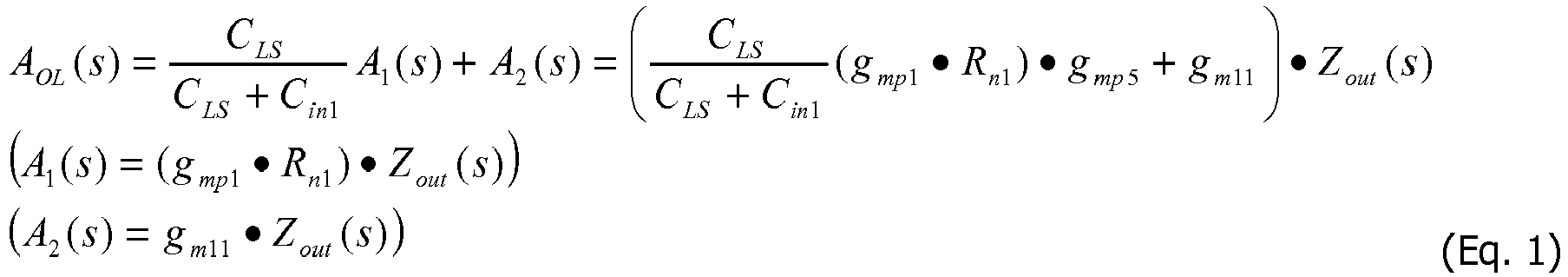
- Equation 1 The open loop gain (AOL) equation of the multi-path amplifier is shown below in Equation 1 (Eq. 1), while amplifier A1 may be associated with the path through INP1/INN1 and the amplifier A2 may be associated with the path through INP2/INN2.
- a 1 s g mp 1 • R n 1 • Z out s
- a 2 s g m 11 • Z out s
- FIG. 5 is one of a plurality of exemplary configurations of the multipath amplifier stage, which, for example, may be used with the pre-amplifier stage shown in the FIG. 4 .
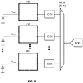
- FIG. 6 illustrates an exemplary implementation according to an embodiment of the present invention.
- the disclosed integration circuit may be used, for example, as a digital X-ray analog front end (AFE).
- AFE can act as a multi-channel data acquisition system, where one channel contains an embodiment of the disclosed integrator (INT) and a correlated double sampling stage (CDS).
- the INT may integrate the charge signal from the photodiode sensor. Any reset noise of the INT may be removed by the CDS stage.
- the acquired signals may be multiplexed and digitized by the MUX and the ADC.
Landscapes
- Engineering & Computer Science (AREA)
- Physics & Mathematics (AREA)
- Mathematical Physics (AREA)
- Theoretical Computer Science (AREA)
- Power Engineering (AREA)
- Software Systems (AREA)
- Computer Hardware Design (AREA)
- General Physics & Mathematics (AREA)
- Amplifiers (AREA)
Description
- Demand for low power electronic devices continues to grow. Circuit designers are increasingly lowering the power provided to electronic devices. However, lower power may have an adverse effect on the dynamic range of components of an electronic device. For example, if an amplifier or comparator device is powered by a lower supply voltage (e.g., 1.8 volts), or lower current supply it limits the range of input signals that can be applied to the device. In order to compensate for the lower power supply in an integrator circuit, for example, a feedback capacitor may need to be larger to accept higher input currents with such a low supply voltage. However, the larger feedback capacitor makes the integrator gain lower and, when the input current signal is lower, the output signal may not be large enough to be detected by a following stage.
- Output noise may also be generated, for example, due to the thermal characteristics of the electrical components (e.g., transistors) of the amplifiers used in the electronic devices, such as integrators. The noise may be propagated upstream thereby causing unacceptable output noises.
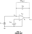
- Circuits that perform integration functions are known in the art as integrators. In a conventional integrator as shown in
FIG. 1 , the input current IIN is integrated across the capacitor CFB. In other words, as IIN changes over time, the voltage VOUT changes inversely to the input current signal. - In more detail, when reset switch SWRESET is CLOSED, the feedback capacitor CFB is discharged, the voltage VIN at the integrator input and output voltage VOUT are reset to equal VREF by the response of the amplifier A1 (after reset VIN = VREF = VOUT).
- When integrating, the reset switch SWRESET is OPEN, and the input signal IIN is applied to the integrator input briefly causing voltage VIN to fluctuate from voltage VREF. The amplifier A1 responds to this fluctuation by outputting a signal to VOUT, so VIN will return to the value VREF. At any time T during integration, the output voltage VOUT may be approximately equal to VREF - (IIN * T/CFB), where T is the time while integrating the current signal IIN.
- Generally, the amplifier A1 outputs an amplified voltage VOUT proportional to the difference between VREF and VIN. However, the amplified voltage output by the amplifier A1 is limited by power supply voltage VDD to the amplifier A1. Amplifier A1 cannot output a voltage higher than VDD or lower than ground as shown in
FIG. 1 . In other words, VOUT will not be greater than VDD. - As mentioned above, circuit designers aim to design circuits having low power and low noise, e.g., thermal noise. The circuit designs require a tradeoff between low power and higher noise, because larger supply current is needed for reducing thermal noise associated with transistors within the amplifiers. Additionally, an external sensor, which may be the input current source IIN, may require higher voltage potentials for proper bias conditions. In the conventional integrator, such as those used in imaging applications, the input current is integrated over time and a representative output voltage is provided. Noise introduced by the amplifiers into the output voltage will be propagated to further devices. Therefore, it is desirable to reduce the amount of noise introduced by the amplifiers of the integrator.
- Noise from amplifiers may result from higher temperatures. The higher temperature (for example, approximately 85 degrees C) can increase thermal noise. One method of reducing thermal noise is to raise the supply current provided by the voltage source of VDD. The lower power consumption of the amplifier by using a lower supply voltage also results in lower noise due to a reduced temperature of the amplifier.
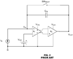
- One known attempt to address this problem has been to put amplifiers in series as shown in
FIG. 2 . The integrator ofFIG. 2 includes a low noise amplifier (LNA) A1, a second amplifier A2, and a feedback capacitor CFB. The LNA A1 that is coupled to a reference voltage VREF on a first input and a current source IIN on a second input. The voltage at the second input is labeled VIN. The LNA A1 is powered by a voltage source VDDL. The second amplifier A2 (not necessarily a low noise amplifier) has inputs coupled to the outputs of LNA A1, and is powered by a second voltage source VDDH. The feedback capacitor CFB is connected to an output of the second amplifier A2 and the VIN node. - While amplifier A2 may be a transconductance amplifier. However, the noise contribution of amplifier A2 is divided by the gain of amplifier A1. Therefore, the noise is generated by amplifier A2 is not as problematic. Noise generated by amplifier A1 may be propagated through to VOUT. The gain of amplifier A1 may be between 5 and 20. The power supply voltage VDDL may be less than 5 volts.
- In contrast to amplifier A1, amplifier A2 may be allowed to be a higher noise source by having a lower supply current and a higher supply voltage VDDH, which may be equal to or greater than 5 volts. The configuration shown in
FIG. 2 realizes lower power, and lower noise with a wider dynamic range than the conventional integrator ofFIG. 1 . However, the input common mode range, represented by VIN, is limited to a lower input potential because the amplifier A1 is supplied with a lower supply voltage VDDL. - Since the supply voltage VDDL of amplifier A1 is low, the reference voltage VREF must be either equal to or less than VDDL. In the integrator shown in
FIG. 2 , the input common mode range VIN is dependent upon the value of VREF, which is limited by Supply voltage VDDL. Due to this limitation, the above configuration may not be suitable for use when the input voltage VIN and the reference voltage VREF need to be higher. For example, when input current source IIN is an external sensor that requires higher potential for its proper bias condition, the integrator confirmation ofFIG. 2 that supplies the input current signal may not be appropriate. - The input device IIN may be a customer device, such as a photodiode. A photodiode typically supplies between 0-5 volts. If 5 volts is applied to amplifier A1, VDDL would have to supply at least that amount of voltage, which would result in higher power consumption of the circuit. In addition, the noise associated with amplifier A1 may be dominated by thermal noise. The thermal noise of amplifier A1 may be reduced if more supply current is consumed. Therefore, in order for amplifier A1 to achieve both low power consumption and low noise, less voltage and more supply current, respectively, is needed to be supplied from VDDL.
-
US 2007/0170981 discloses a chopper stabilized amplifier circuit having an input chopper and an output chopper for chopping an output signal of a first operational transconductance amplifier. The device further comprises a switched capacitor notch filter for filtering out the ripple voltages which are produced by the output chopper. - Accordingly, another more flexible solution is needed. There is a need for a low power, low noise integrating device that provides acceptable bias conditions.
-
-
FIG. 1 illustrates a conventional integrator circuit. -
FIG. 2 illustrates a conventional multi-stage integrator circuit. -
FIG. 3 illustrates an exemplary circuit diagram according to an embodiment of the invention. -
FIG. 4 illustrates an exemplary implementation of a pre-amplifier stage of an embodiment of the present invention. -
FIG. 5 illustrates an exemplary implementation of a multipath amplifier stage of an embodiment of the present invention. -
FIG. 6 illustrates an exemplary application according to an embodiment of the present invention. - Embodiments of the present invention provide an integrator configuration that may include a level-shifting capacitor, a feedback capacitor, a switch module, a pre-amplifier stage and a multi-path amplifier module. The integrator may have inputs for connecting an input signal source to the level-shifting capacitor. The level-shifting capacitor may be connected to an input of a pre-amplifier stage of an integration signal path and to an input of the integrator circuit. The level-shifting capacitor may level shift the voltage at the input of the integrator circuit to a lower voltage at the input of the pre-amplifier stage. Thereby, the supply voltage to the pre-amplifier stage may be reduced as well as limiting power consumption, limiting temperature rise, and reducing noise attributed to any thermal effects on the amplifier.
-
FIG. 3 illustrates an exemplary circuit diagram according to an embodiment of the invention. Theintegrator 300 may include apre-amplifier stage 310, a level-shiftingcapacitor C LS 307, afeedback capacitor C FB 303, amulti-path amplifier module 320, and a reset switches 323A and 323B. Reset switches 323A and 323B may be implemented using transistors. - The
pre-amplifier stage 310 may include anamplifier 313. Theamplifier 313 may be a low noise amplifier, which may be characterized by a high supply current. In addition, theamplifier 313 can have a low thermal noise voltage density of about 2nV/sqrt(Hz). Theamplifier 313 may have a first input, a second input, a power supply input terminal, and a pair of outputs (a first output and a second output). The first input may be connected to a terminal of levelshift capacitor C LS 307 and a first terminal ofreset switch 323A. The second input may be connected to a pre-amplifier stage reference voltage source VREF-LO and to a second terminal ofreset switch 323A. The power supply input terminal may be connected to voltage source VDDL, which may be in thepre-amplifier stage 310 or may be an external voltage source. The pair of outputs may be connected to inputs of theamplifier module 320. The pair of outputs may be differential outputs. -
Multi-path amplifier module 320 may include a first amplifier AINT and second amplifier ARESET. Amplifier AINT may have inputs connected to A1 the outputs of pre-amplifier stage 413, a power supply input connected to voltage source VDDH, and an output connected to VOUT, the second terminal offeedback capacitor CFB 303 and second terminal ofreset switch 323B. - The supply voltage VDDL to the
pre-amplifier stage 310 may be lower than the supply voltage VDDH to themulti-path amplifier module 320. A higher input voltage up to the value of supply voltage VDDH may be applied to theintegrator 300, while still utilizing the lower supply voltage VDDL for thepre-amplifier 310. Being able to use the lower supply voltage VDDL may be facilitated by the inclusion of the level-shiftingcapacitor C LS 307 that reduces the input voltage to thepre-amplifier 310. For example, the supply voltage VDDH may be 5 volts, while the supply voltage VDDL may be 1.8 volts. The supply voltage VDDL may be lower than the input voltage VIN. The input voltage VIN may be 4-5 volts. Generally, this allows supply voltage VDDL to be set independent of VIN. - The level shifting
capacitor C LS 307 may be connected to a first terminal offeedback capacitor C FB 303, to resetswitch 323B and an input in the reset circuit path to amplifier ARESET of theamplifier module 320. Thecapacitor C LS 307 may also be connected to a signal input of thepre-amplifier stage 310 and resetswitch 323A. - The
feedback capacitor C FB 303 may be connected to a first terminal ofreset switch 323B, the first terminal of level-shiftingcapacitor C LS 307, and an input in the reset circuit path to amplifier ARESET of theamplifier module 320.Capacitor CFB 303 may also be connected to both the output VOUT ofamplifier module 320 and to a second terminal of thereset switch 323B. As shown inFIG. 3 , thereset switch 323B is connected in parallel to thefeedback capacitor C FB 303. - Referring back to the
multi-path amplifier module 320, the inputs INP1/INN1 of amplifier AINT may receive respective differential signals output fromamplifier 313 of thepre-amplifier stage 310. - Amplifier AINT may be a transconductance amplifier, and may have different circuit parameter than amplifier ARESET because AINT may have, for example, different electrical requirements.
- Amplifier ARESET may have its inputs connected to VREF-HI and VIN, respectively; a power supply input connected to voltage source VDDH; and an output connected to VOUT. The inputs INP2/INN2 of amplifier ARESET may receive respective signals VREF-HI and VIN. Amplifier ARESET may also be a transconductance amplifier.
- The outputs of the amplifier AINT and the amplifier ARESET may be connected together at VOUT. The combined gain of the
pre-amplifier 310 and amplifier AINT may be greater than the gain of amplifier ARESET. - Amplifier power supply voltages VDDL and VDDH may be provided from external sources to facilitate the programmability of the
integrator 300. Optionally, voltage sources VDDL and VDDH may either be included inintegrator 300 or externally, and have predetermined settings or programmable settings. In either case, VDDL may be set independent of the input signal source IIN 350 and its related VIN. - The foregoing embodiments permit the amplifier power supply voltages VDDL and VDDH to be set at different levels. The power supply voltage VDDL may be set lower than VDDH. The configuration of the forgoing embodiments may provide a designer with the capability to set the integrator's input bias voltage independent of the power supply voltage VDDL for the pre-amplifier stage thereby effectively balancing the need for a sufficiently high output voltage with the need for reduced power consumption and reduced noise characteristics.
- In an embodiment, the reference voltage VREF-LO may have a value of approximately 1.0 volt and reference voltage VREF-HI can have a value as high as approximately 5 volts. The
multipath amplifier 320 may have inputs INN1 and INP1 connected to outputs of thepre-amplifier 310, and inputs INN2 and INP2 connected, respectively, to theinput 390 of theintegrator 300 and a reference voltage VREF-HI. - The
integrator 300 may operate in either a reset mode or an integration mode. When in reset mode, theswitches circuit 300 resets the input voltage VIN to reference voltage VREF-HI, and the voltage at the input of thepre-amplifier stage 310 may be reset to reference voltage VREF-LO. Thecapacitor C FB 303 may be discharged because of the short circuit created by theclosed switch 323B. The inputs to thepre-amplifier stage 310 are shorted, soamplifier 313 does not have an appreciable output, and the voltage at the inverting input ofamplifier 313 may be reset to VREF-LO. Also at reset, thecapacitor C LS 307 is charged to a value of VCLS, which may be equal to VREF-HI minus VREF-LO. After completion of the above operations, theintegrator 300 is now reset to integrate the next input signal. - In integration mode, the
switches integrator 300 functions as an integrator. A signal from an input current source IIN 350 may be applied to theintegrator 300 atinput 390. The input current signal may be integrated overcapacitor C FB 303 as previously explained. - The voltage VIN may fluctuate from VREF-HI, in which case the
pre-amplifier 310 and themultipath amplifier 320 respond to return, via the feedback path throughfeedback capacitor C FB 303, the voltage VIN to VREF-HI. The levelshift capacitor C LS 307, which may act as a floating voltage source, and has been charged to a voltage VCLS at reset, may reduce the voltage VIN to a voltage approximately equal to VIN - VCLS that may be maintained at the inverting input ofamplifier 313. - The voltages VIN-VCLS and VREF-LO may be less than the power supply voltage of VDDL of
amplifier 313. Theamplifier 313 may output differential voltages to the inputs INN1/INP1 of themultipath amplifier 320 representative of the difference between the values of VIN-VCLS and VREF-LO. The differential voltages received on inputs INN1/INP1 may be input into a transconductance amplifier AINT, which may output a gained current that may be proportional to the difference of the differential voltages received on inputs INN1/INP1. -
Multipath amplifier 320 may also have inputs INN2/INP2 that may receive the voltages VIN and VREF-HI, respectively. The voltages on inputs INN2/INP2 may be input into the transconductance amplifier ARESET, which may output a gained current proportional to the difference of the voltages VIN and VREF-HI. The current outputs of the amplifiers AINT and ARESET may be connected together, so the outputs of each are combined, and output to VOUT. Via the feedback path throughfeedback capacitor C FB 303, the voltage VIN is returned to VREF-HI. After the input current signal from current source IIN 350 is integrated for a predetermined time period, theintegrator 300 enters a reset mode, and is reset to a reference voltage as previously explained above. - Generally, VIN may be approximately 4-5 volts, while the power supply voltage VDDL to
amplifier 313 may be approximately 1.8 volts. Consequently, the input voltage at the inverting input ofamplifier 313 may be expected to be lower than or approximately equal to the voltage VDDL due to the level-shifting ofcapacitor C LS 307. The input to the inverting input ofamplifier 313 may be maintained at a voltage of approximately VIN - VCLS, which may be approximately equal to VREF-LO. The voltage VCLS may be expected to have minimal change from its voltage at reset. Thereby, the level-shift capacitor may reduces the voltage level of an input by the voltage VCLS to a voltage level that is less than or equal to the supply voltage VDDL. Overall, the noise and the power consumption of thecircuit 300 may be reduced in comparison to prior art systems because the lower supply voltage VDDL with a higher supply current may be used. - An exemplary circuit diagram of the pre-amplifier and the multipath amplifier are shown respectively in
FIGS. 4 and5 .FIG. 4 illustrates one of a plurality of exemplary configurations for a pre-amplifier stage according to an embodiment of the present invention. - The exemplary pre-amplifier stage may have multiple stages. For example, a first stage may have a P-channel input pair with Mp1 and Mp2, and may have load resistors of Rn1 and Rn2, to form a wide band amplifier with fixed gain. The gain may be given by gmp1*Rn1 where gmp1 represents a transconductance of the Mp1 and the Mp2. For example, a second stage may have another P-channel input pair with Mp5 and Mp6 and may have current sources of Mn1 and Mn2, to form a transconductance amplifier. The transconductance of this stage may be gmp5, which is the transconductance of the Mp5 and the Mp6.
- The exemplary first and second stage may operate in a reset mode and an integration mode. During the reset mode, switches Sw3 and Sw4, driven by PIRST_B, may be open so that the pre-amplifier stage may be disconnected from the multipath amplifier. In the meantime, Sw1 and Sw2 may be closed to perform an auto-zero function, so that a null voltage is stored at auto-zero capacitors C1 and C2.
- During the integration mode, the switches Sw1 and the Sw2 may be open, and the null voltage at the capacitors C1 and C2 may be maintained to null out any offset current at the output terminal (OUTP/OUTN). The switches Sw3 and the Sw4 may be closed to connect to representative ones of the differential outputs OUTN and OUTP, which are connected to respective input terminals of the amplifier A2 (INP1/INN1).
-
Fig. 5 illustrates an embodiment of an exemplary multipath amplifier with multi-differential inputs according to an embodiment of the present invention. The exemplary multipath amplifier may receive differential input voltages on INN1 and INP1. InFig. 5 , the multipath amplifier may have both an N-channel input pair with Mn11/Mn12 and a P-channel input pair with Mp11/Mp12, to accommodate either higher or lower input common mode voltage at the INP2/INN2 terminal. The multipath amplifier may employ a folded cascode stage to enhance the DC gain. A folded cascode stage may contain a PMOS current mirror (Mp15, Mp16, M17, and Mp18), and a NMOS current sources (Mn15, Mn16, Mn17, and Mn18). The multipath amplifier may have another differential input (INP1/INN1) at the source of the Mn17 and the Mn18, to receive the current signal from the A1. - In operation, the embodiment of
FIG. 5 may also operate in two modes: a reset mode and an integration mode. During the reset mode, the INP1/INN1 may be isolated from amplifier A1 and the inputs INP2/INN2 may be the only active inputs. By the feedback operation, the voltage at the INN2 and the OUT output voltage are forced to the voltage VREF-HI. During the integration mode, the INP1/INN1 is connected to the output of the pre-amplifier stage ofFIG. 4 to receive its output current. - The open loop gain (AOL) equation of the multi-path amplifier is shown below in Equation 1 (Eq. 1), while amplifier A1 may be associated with the path through INP1/INN1 and the amplifier A2 may be associated with the path through INP2/INN2.
-
FIG. 5 is one of a plurality of exemplary configurations of the multipath amplifier stage, which, for example, may be used with the pre-amplifier stage shown in theFIG. 4 . - The disclosed integration circuit may be employed in a plurality of applications. One such application is illustrated in
FIG. 6. FIG. 6 illustrates an exemplary implementation according to an embodiment of the present invention. - The disclosed integration circuit may be used, for example, as a digital X-ray analog front end (AFE). The AFE can act as a multi-channel data acquisition system, where one channel contains an embodiment of the disclosed integrator (INT) and a correlated double sampling stage (CDS). The INT may integrate the charge signal from the photodiode sensor. Any reset noise of the INT may be removed by the CDS stage. The acquired signals may be multiplexed and digitized by the MUX and the ADC.
- Several features and aspects of the present invention have been illustrated and described in detail with reference to particular embodiments by way of example only, and not by way of limitation. Those of skill in the art will appreciate that alternative implementations and various modifications to the disclosed embodiments are within the scope of the present disclosure.
Claims (8)
- An integrator circuit (300), comprising:a pre-amplifier stage (310) having a first input, a second input for a reference voltage, and an input for a first power supply voltage (VDDL);a multi-path amplifier module (320) having a first amplification path connected between an input and an output of the integrator circuit (300), the first amplification path comprising a first amplifier stage (AReset), a second amplification path connected between the pre-amplifier stage (310) and the output of the integrator circuit (300), the second amplification path comprising a second amplifier stage (AInt), and the first and second amplifier stages each having an input for a second power supply voltage (VDDH), wherein the second power supply voltage (VDDH) is greater than the first supply power voltage (VDDL), and each having an output connected to an output of the integrator circuit (300);a level-shifting capacitor (CLS) connected to the input of the integrator circuit, and to the first input of the pre-amplifier stage (310), wherein the level-shifting capacitor (CLS) provides a reduced voltage input to the pre-amplifier stage (310); anda feedback capacitor (CFB) connected between the input and the output of the integrator circuit.
- The integrator circuit (300) of claim 1, comprising:a plurality of switches (323A, 323B), wherein when a first of the plurality of switches (323A) is closed, a circuit path across the first and second inputs of the pre-amplifier circuit (313) is created, and when a second of the plurality of switches (323B) is closed, a circuit path that short circuits the feedback capacitor (CFB) is created.
- The integrator circuit (300) of claim 1, wherein the first supply voltage (VDDL) is provided either from within the pre-amplifier stage (310) or by an external voltage source.
- The integrator circuit (300) of claim 1, the preamplifier stage (310) further comprising:a pair of differential outputs that output a difference between the reduced input voltage and a preamplifier stage (310) reference voltage.
- The integrator circuit (300) of claim 1, wherein the level-shift capacitor (CLS) reduces the voltage level of an input (Vin) to a voltage level that is less than or equal to the first supply voltage (VDDL).
- The integrator circuit (300) of claim 1, wherein the multi-path amplifier module (320) comprises:a first transconductance amplifier stage (ARESET) in the first amplification path, wherein an input to the first amplifier stage is a multi-path amplifier reference voltage and the input voltage of the integrator, and a second transconductance amplifier stage (AINT) in the second amplification path, wherein the second amplifier stage has inputs for receiving differential voltages from the pre-amplifier stage (310).
- The integrator circuit (300) of claim 2, wherein when the switches (323A, 323B) are in a closed position, the voltage at the input of the pre-amplifier stage (310) is set to a first reference voltage, and the voltage at the input and the output of the integrator circuit (300) is set to a second reference voltage.
- A method for integrating an input current signal in a reduced power integrator circuit (300) according to any one of claims 1 to 7, comprising:providing a first power supply voltage (VDDL) to a first amplifier stage;providing a second power supply voltage (VDDH) to a second amplifier stage, wherein the second power supply voltage (VDDH) is greater than the first power supply voltage (VDDL);receiving an input at the input of the integrator,applying the input to a level-shifting capacitor (CLS) and at an input to the second amplifier stage;applying a reduced voltage from the level-shifting capacitor (CLS) to the first amplifier stage, wherein the reduced voltage is less than or equal to the first power supply voltage (VDDL);outputting a differential amplified voltage from the first amplifier stage based on the reduced input voltage compared to a low reference voltage to a third amplifier stage;in the third amplifier stage, amplifying the difference of the differential amplified voltage and outputting a first amplified output signal;outputting a second amplified signal from the second amplifier stage based on the input voltage compared to a high reference voltage;combining the first amplified signal and the second amplified signal at the output of the integrator circuit (300); andintegrating the input current signal over a feedback capacitor (CFB) connected in parallel to the first, second and third amplifier stages and connecting the input of the integrator to the output of the integrator.
Applications Claiming Priority (3)
| Application Number | Priority Date | Filing Date | Title |
|---|---|---|---|
| US23522609P | 2009-08-19 | 2009-08-19 | |
| US12/726,455 US8125262B2 (en) | 2009-08-19 | 2010-03-18 | Low power and low noise switched capacitor integrator with flexible input common mode range |
| PCT/US2010/044864 WO2011022232A1 (en) | 2009-08-19 | 2010-08-09 | Low power and low noise switched capacitor integrator with flexible input common mode range |
Publications (3)
| Publication Number | Publication Date |
|---|---|
| EP2467775A1 EP2467775A1 (en) | 2012-06-27 |
| EP2467775A4 EP2467775A4 (en) | 2015-05-06 |
| EP2467775B1 true EP2467775B1 (en) | 2017-08-02 |
Family
ID=43604853
Family Applications (1)
| Application Number | Title | Priority Date | Filing Date |
|---|---|---|---|
| EP10810385.4A Active EP2467775B1 (en) | 2009-08-19 | 2010-08-09 | Low power and low noise switched capacitor integrator with flexible input common mode range |
Country Status (3)
| Country | Link |
|---|---|
| US (1) | US8125262B2 (en) |
| EP (1) | EP2467775B1 (en) |
| WO (1) | WO2011022232A1 (en) |
Families Citing this family (16)
| Publication number | Priority date | Publication date | Assignee | Title |
|---|---|---|---|---|
| US8502522B2 (en) | 2010-04-28 | 2013-08-06 | Teradyne, Inc. | Multi-level triggering circuit |
| US8531176B2 (en) * | 2010-04-28 | 2013-09-10 | Teradyne, Inc. | Driving an electronic instrument |
| US8542005B2 (en) | 2010-04-28 | 2013-09-24 | Teradyne, Inc. | Connecting digital storage oscilloscopes |
| US9048805B2 (en) | 2011-10-04 | 2015-06-02 | Rf Micro Devices, Inc. | Tunable duplexer architecture |
| US9190979B2 (en) | 2012-02-07 | 2015-11-17 | Rf Micro Devices, Inc. | Hybrid coupler |
| US9071430B2 (en) * | 2012-02-07 | 2015-06-30 | Rf Micro Devices, Inc. | RF transceiver with distributed filtering topology |
| US8952751B2 (en) | 2012-12-31 | 2015-02-10 | Silicon Laboratories Inc. | Amplifier circuits and methods of amplifying an input signal |
| US8803569B1 (en) | 2013-06-27 | 2014-08-12 | International Business Machines Corporation | Ramp generator using operational amplifier based integration and switched capacitor techniques |
| US9787291B1 (en) | 2016-12-20 | 2017-10-10 | Infineon Technologies Ag | System and method for a switched capacitor circuit |
| US10673389B2 (en) | 2017-11-20 | 2020-06-02 | Linear Technology Holding Llc | Chopper amplifiers with high pass filter for suppressing chopping ripple |
| US10735045B2 (en) | 2018-04-23 | 2020-08-04 | Qorvo Us, Inc. | Diplexer circuit |
| US11025214B2 (en) * | 2019-01-28 | 2021-06-01 | Intel Corporation | Low voltage class AB operational trans-conductance amplifier |
| US10897261B1 (en) * | 2020-03-05 | 2021-01-19 | Infineon Technologies Ag | Analog-to-digital converter with a supplementary digital-to-analog converter for offset and gain error measurements |
| CN112929017B (en) * | 2021-02-02 | 2023-08-18 | 同源微(北京)半导体技术有限公司 | Integrator circuit for improving reset speed |
| FR3120741B1 (en) * | 2021-03-09 | 2023-12-08 | St Microelectronics Alps Sas | Photosensitive device comprising an integrator circuit per group of at least two photosensitive elements. |
| JP2022148472A (en) * | 2021-03-24 | 2022-10-06 | 株式会社ミツトヨ | Front end circuit and encoder |
Family Cites Families (7)
| Publication number | Priority date | Publication date | Assignee | Title |
|---|---|---|---|---|
| US6002299A (en) * | 1997-06-10 | 1999-12-14 | Cirrus Logic, Inc. | High-order multipath operational amplifier with dynamic offset reduction, controlled saturation current limiting, and current feedback for enhanced conditional stability |
| US6703894B1 (en) * | 2003-01-13 | 2004-03-09 | Standard Microsystems Corporation | Baseband filter for receivers |
| US7044571B2 (en) * | 2003-10-28 | 2006-05-16 | Hewlett-Packard Development Company, L.P. | Power supply adjustment |
| US7292095B2 (en) * | 2006-01-26 | 2007-11-06 | Texas Instruments Incorporated | Notch filter for ripple reduction in chopper stabilized amplifiers |
| US7345530B1 (en) * | 2006-06-01 | 2008-03-18 | National Semiconductor Corporation | Regulated switch driving scheme in switched-capacitor amplifiers with opamp-sharing |
| US7595678B2 (en) * | 2006-09-11 | 2009-09-29 | The Board Of Regents, University Of Texas System | Switched-capacitor circuit |
| US7973596B2 (en) * | 2009-05-12 | 2011-07-05 | Number 14 B.V. | Low-noise, low-power, low drift offset correction in operational and instrumentation amplifiers |
-
2010
- 2010-03-18 US US12/726,455 patent/US8125262B2/en active Active
- 2010-08-09 EP EP10810385.4A patent/EP2467775B1/en active Active
- 2010-08-09 WO PCT/US2010/044864 patent/WO2011022232A1/en not_active Ceased
Non-Patent Citations (1)
| Title |
|---|
| None * |
Also Published As
| Publication number | Publication date |
|---|---|
| EP2467775A1 (en) | 2012-06-27 |
| US20110043270A1 (en) | 2011-02-24 |
| EP2467775A4 (en) | 2015-05-06 |
| US8125262B2 (en) | 2012-02-28 |
| WO2011022232A1 (en) | 2011-02-24 |
Similar Documents
| Publication | Publication Date | Title |
|---|---|---|
| EP2467775B1 (en) | Low power and low noise switched capacitor integrator with flexible input common mode range | |
| US7586373B2 (en) | Fully differential class AB amplifier and amplifying method using single-ended, two-stage amplifier | |
| US6462612B1 (en) | Chopper stabilized bandgap reference circuit to cancel offset variation | |
| EP0295221B1 (en) | Cmos power operational amplifier | |
| EP2781017B1 (en) | Low noise auto-zero circuits for amplifiers | |
| KR101916224B1 (en) | Amplifier for output buffer and signal processing apparatus using thereof | |
| EP2611028A1 (en) | Multi-stage fully differential amplifier with controlled common mode voltage | |
| EP2466745A1 (en) | Amplifier common-mode control methods | |
| US5789981A (en) | High-gain operational transconductance amplifier offering improved bandwidth | |
| US6538503B2 (en) | Instrumentation amplifier and method for obtaining high common mode rejection | |
| JP2000517146A (en) | Gm-C cell with two-stage common mode control and current boost means | |
| US5361040A (en) | Self limiting and self biasing operational transconductance amplifier | |
| JP4515241B2 (en) | Output amplifier circuit and sensor device using the same | |
| US6888407B2 (en) | Multistage differential amplifier with CMFB circuit | |
| US11811373B2 (en) | Class AB amplifier and operational amplifier | |
| US6160446A (en) | Balanced differential amplifier without common-mode feedback circuit | |
| US6833760B1 (en) | Low power differential amplifier powered by multiple unequal power supply voltages | |
| US20080284634A1 (en) | Differential amplifying circuit | |
| EP1835624A2 (en) | Power management in a data acquisition system | |
| US7554405B2 (en) | Adaptive biasing input stage and amplifiers including the same | |
| US7202746B1 (en) | Multiple-stage operational amplifier and methods and systems utilizing the same | |
| KR101122581B1 (en) | Constant voltage potentiostat circuit using differencial difference amplifier | |
| WO2004017514A1 (en) | Operational amplifier | |
| EP3918710B1 (en) | Amplifier circuit | |
| US7199655B2 (en) | Multistage amplifier circuit without interstage coupling capacitor |
Legal Events
| Date | Code | Title | Description |
|---|---|---|---|
| PUAI | Public reference made under article 153(3) epc to a published international application that has entered the european phase |
Free format text: ORIGINAL CODE: 0009012 |
|
| 17P | Request for examination filed |
Effective date: 20120210 |
|
| AK | Designated contracting states |
Kind code of ref document: A1 Designated state(s): AL AT BE BG CH CY CZ DE DK EE ES FI FR GB GR HR HU IE IS IT LI LT LU LV MC MK MT NL NO PL PT RO SE SI SK SM TR |
|
| DAX | Request for extension of the european patent (deleted) | ||
| REG | Reference to a national code |
Ref country code: DE Ref legal event code: R079 Ref document number: 602010044136 Country of ref document: DE Free format text: PREVIOUS MAIN CLASS: G06F0007640000 Ipc: G06G0007186000 |
|
| RA4 | Supplementary search report drawn up and despatched (corrected) |
Effective date: 20150409 |
|
| RIC1 | Information provided on ipc code assigned before grant |
Ipc: G06G 7/186 20060101AFI20150401BHEP |
|
| 17Q | First examination report despatched |
Effective date: 20151208 |
|
| GRAP | Despatch of communication of intention to grant a patent |
Free format text: ORIGINAL CODE: EPIDOSNIGR1 |
|
| STAA | Information on the status of an ep patent application or granted ep patent |
Free format text: STATUS: GRANT OF PATENT IS INTENDED |
|
| INTG | Intention to grant announced |
Effective date: 20170302 |
|
| GRAS | Grant fee paid |
Free format text: ORIGINAL CODE: EPIDOSNIGR3 |
|
| GRAA | (expected) grant |
Free format text: ORIGINAL CODE: 0009210 |
|
| STAA | Information on the status of an ep patent application or granted ep patent |
Free format text: STATUS: THE PATENT HAS BEEN GRANTED |
|
| AK | Designated contracting states |
Kind code of ref document: B1 Designated state(s): AL AT BE BG CH CY CZ DE DK EE ES FI FR GB GR HR HU IE IS IT LI LT LU LV MC MK MT NL NO PL PT RO SE SI SK SM TR |
|
| REG | Reference to a national code |
Ref country code: GB Ref legal event code: FG4D |
|
| REG | Reference to a national code |
Ref country code: CH Ref legal event code: EP Ref country code: AT Ref legal event code: REF Ref document number: 915227 Country of ref document: AT Kind code of ref document: T Effective date: 20170815 |
|
| REG | Reference to a national code |
Ref country code: IE Ref legal event code: FG4D |
|
| REG | Reference to a national code |
Ref country code: DE Ref legal event code: R096 Ref document number: 602010044136 Country of ref document: DE |
|
| REG | Reference to a national code |
Ref country code: NL Ref legal event code: MP Effective date: 20170802 |
|
| REG | Reference to a national code |
Ref country code: AT Ref legal event code: MK05 Ref document number: 915227 Country of ref document: AT Kind code of ref document: T Effective date: 20170802 |
|
| REG | Reference to a national code |
Ref country code: LT Ref legal event code: MG4D |
|
| PG25 | Lapsed in a contracting state [announced via postgrant information from national office to epo] |
Ref country code: NL Free format text: LAPSE BECAUSE OF FAILURE TO SUBMIT A TRANSLATION OF THE DESCRIPTION OR TO PAY THE FEE WITHIN THE PRESCRIBED TIME-LIMIT Effective date: 20170802 Ref country code: LT Free format text: LAPSE BECAUSE OF FAILURE TO SUBMIT A TRANSLATION OF THE DESCRIPTION OR TO PAY THE FEE WITHIN THE PRESCRIBED TIME-LIMIT Effective date: 20170802 Ref country code: HR Free format text: LAPSE BECAUSE OF FAILURE TO SUBMIT A TRANSLATION OF THE DESCRIPTION OR TO PAY THE FEE WITHIN THE PRESCRIBED TIME-LIMIT Effective date: 20170802 Ref country code: AT Free format text: LAPSE BECAUSE OF FAILURE TO SUBMIT A TRANSLATION OF THE DESCRIPTION OR TO PAY THE FEE WITHIN THE PRESCRIBED TIME-LIMIT Effective date: 20170802 Ref country code: FI Free format text: LAPSE BECAUSE OF FAILURE TO SUBMIT A TRANSLATION OF THE DESCRIPTION OR TO PAY THE FEE WITHIN THE PRESCRIBED TIME-LIMIT Effective date: 20170802 Ref country code: NO Free format text: LAPSE BECAUSE OF FAILURE TO SUBMIT A TRANSLATION OF THE DESCRIPTION OR TO PAY THE FEE WITHIN THE PRESCRIBED TIME-LIMIT Effective date: 20171102 Ref country code: SE Free format text: LAPSE BECAUSE OF FAILURE TO SUBMIT A TRANSLATION OF THE DESCRIPTION OR TO PAY THE FEE WITHIN THE PRESCRIBED TIME-LIMIT Effective date: 20170802 |
|
| PG25 | Lapsed in a contracting state [announced via postgrant information from national office to epo] |
Ref country code: GR Free format text: LAPSE BECAUSE OF FAILURE TO SUBMIT A TRANSLATION OF THE DESCRIPTION OR TO PAY THE FEE WITHIN THE PRESCRIBED TIME-LIMIT Effective date: 20171103 Ref country code: ES Free format text: LAPSE BECAUSE OF FAILURE TO SUBMIT A TRANSLATION OF THE DESCRIPTION OR TO PAY THE FEE WITHIN THE PRESCRIBED TIME-LIMIT Effective date: 20170802 Ref country code: BG Free format text: LAPSE BECAUSE OF FAILURE TO SUBMIT A TRANSLATION OF THE DESCRIPTION OR TO PAY THE FEE WITHIN THE PRESCRIBED TIME-LIMIT Effective date: 20171102 Ref country code: LV Free format text: LAPSE BECAUSE OF FAILURE TO SUBMIT A TRANSLATION OF THE DESCRIPTION OR TO PAY THE FEE WITHIN THE PRESCRIBED TIME-LIMIT Effective date: 20170802 Ref country code: IS Free format text: LAPSE BECAUSE OF FAILURE TO SUBMIT A TRANSLATION OF THE DESCRIPTION OR TO PAY THE FEE WITHIN THE PRESCRIBED TIME-LIMIT Effective date: 20171202 Ref country code: PL Free format text: LAPSE BECAUSE OF FAILURE TO SUBMIT A TRANSLATION OF THE DESCRIPTION OR TO PAY THE FEE WITHIN THE PRESCRIBED TIME-LIMIT Effective date: 20170802 |
|
| REG | Reference to a national code |
Ref country code: CH Ref legal event code: PL |
|
| PG25 | Lapsed in a contracting state [announced via postgrant information from national office to epo] |
Ref country code: CH Free format text: LAPSE BECAUSE OF NON-PAYMENT OF DUE FEES Effective date: 20170831 Ref country code: CZ Free format text: LAPSE BECAUSE OF FAILURE TO SUBMIT A TRANSLATION OF THE DESCRIPTION OR TO PAY THE FEE WITHIN THE PRESCRIBED TIME-LIMIT Effective date: 20170802 Ref country code: DK Free format text: LAPSE BECAUSE OF FAILURE TO SUBMIT A TRANSLATION OF THE DESCRIPTION OR TO PAY THE FEE WITHIN THE PRESCRIBED TIME-LIMIT Effective date: 20170802 Ref country code: RO Free format text: LAPSE BECAUSE OF FAILURE TO SUBMIT A TRANSLATION OF THE DESCRIPTION OR TO PAY THE FEE WITHIN THE PRESCRIBED TIME-LIMIT Effective date: 20170802 Ref country code: LI Free format text: LAPSE BECAUSE OF NON-PAYMENT OF DUE FEES Effective date: 20170831 |
|
| REG | Reference to a national code |
Ref country code: DE Ref legal event code: R097 Ref document number: 602010044136 Country of ref document: DE Ref country code: BE Ref legal event code: MM Effective date: 20170831 |
|
| REG | Reference to a national code |
Ref country code: IE Ref legal event code: MM4A |
|
| PG25 | Lapsed in a contracting state [announced via postgrant information from national office to epo] |
Ref country code: SK Free format text: LAPSE BECAUSE OF FAILURE TO SUBMIT A TRANSLATION OF THE DESCRIPTION OR TO PAY THE FEE WITHIN THE PRESCRIBED TIME-LIMIT Effective date: 20170802 Ref country code: MC Free format text: LAPSE BECAUSE OF FAILURE TO SUBMIT A TRANSLATION OF THE DESCRIPTION OR TO PAY THE FEE WITHIN THE PRESCRIBED TIME-LIMIT Effective date: 20170802 Ref country code: EE Free format text: LAPSE BECAUSE OF FAILURE TO SUBMIT A TRANSLATION OF THE DESCRIPTION OR TO PAY THE FEE WITHIN THE PRESCRIBED TIME-LIMIT Effective date: 20170802 Ref country code: SM Free format text: LAPSE BECAUSE OF FAILURE TO SUBMIT A TRANSLATION OF THE DESCRIPTION OR TO PAY THE FEE WITHIN THE PRESCRIBED TIME-LIMIT Effective date: 20170802 Ref country code: IT Free format text: LAPSE BECAUSE OF FAILURE TO SUBMIT A TRANSLATION OF THE DESCRIPTION OR TO PAY THE FEE WITHIN THE PRESCRIBED TIME-LIMIT Effective date: 20170802 |
|
| PLBE | No opposition filed within time limit |
Free format text: ORIGINAL CODE: 0009261 |
|
| STAA | Information on the status of an ep patent application or granted ep patent |
Free format text: STATUS: NO OPPOSITION FILED WITHIN TIME LIMIT |
|
| PG25 | Lapsed in a contracting state [announced via postgrant information from national office to epo] |
Ref country code: LU Free format text: LAPSE BECAUSE OF NON-PAYMENT OF DUE FEES Effective date: 20170809 |
|
| REG | Reference to a national code |
Ref country code: FR Ref legal event code: ST Effective date: 20180607 |
|
| 26N | No opposition filed |
Effective date: 20180503 |
|
| PG25 | Lapsed in a contracting state [announced via postgrant information from national office to epo] |
Ref country code: IE Free format text: LAPSE BECAUSE OF NON-PAYMENT OF DUE FEES Effective date: 20170809 |
|
| PG25 | Lapsed in a contracting state [announced via postgrant information from national office to epo] |
Ref country code: BE Free format text: LAPSE BECAUSE OF NON-PAYMENT OF DUE FEES Effective date: 20170831 Ref country code: FR Free format text: LAPSE BECAUSE OF NON-PAYMENT OF DUE FEES Effective date: 20171002 Ref country code: SI Free format text: LAPSE BECAUSE OF FAILURE TO SUBMIT A TRANSLATION OF THE DESCRIPTION OR TO PAY THE FEE WITHIN THE PRESCRIBED TIME-LIMIT Effective date: 20170802 |
|
| PG25 | Lapsed in a contracting state [announced via postgrant information from national office to epo] |
Ref country code: MT Free format text: LAPSE BECAUSE OF NON-PAYMENT OF DUE FEES Effective date: 20170809 |
|
| PG25 | Lapsed in a contracting state [announced via postgrant information from national office to epo] |
Ref country code: HU Free format text: LAPSE BECAUSE OF FAILURE TO SUBMIT A TRANSLATION OF THE DESCRIPTION OR TO PAY THE FEE WITHIN THE PRESCRIBED TIME-LIMIT; INVALID AB INITIO Effective date: 20100809 |
|
| PG25 | Lapsed in a contracting state [announced via postgrant information from national office to epo] |
Ref country code: CY Free format text: LAPSE BECAUSE OF NON-PAYMENT OF DUE FEES Effective date: 20170802 |
|
| PG25 | Lapsed in a contracting state [announced via postgrant information from national office to epo] |
Ref country code: MK Free format text: LAPSE BECAUSE OF FAILURE TO SUBMIT A TRANSLATION OF THE DESCRIPTION OR TO PAY THE FEE WITHIN THE PRESCRIBED TIME-LIMIT Effective date: 20170802 |
|
| PG25 | Lapsed in a contracting state [announced via postgrant information from national office to epo] |
Ref country code: TR Free format text: LAPSE BECAUSE OF FAILURE TO SUBMIT A TRANSLATION OF THE DESCRIPTION OR TO PAY THE FEE WITHIN THE PRESCRIBED TIME-LIMIT Effective date: 20170802 |
|
| PG25 | Lapsed in a contracting state [announced via postgrant information from national office to epo] |
Ref country code: PT Free format text: LAPSE BECAUSE OF FAILURE TO SUBMIT A TRANSLATION OF THE DESCRIPTION OR TO PAY THE FEE WITHIN THE PRESCRIBED TIME-LIMIT Effective date: 20170802 |
|
| PG25 | Lapsed in a contracting state [announced via postgrant information from national office to epo] |
Ref country code: AL Free format text: LAPSE BECAUSE OF FAILURE TO SUBMIT A TRANSLATION OF THE DESCRIPTION OR TO PAY THE FEE WITHIN THE PRESCRIBED TIME-LIMIT Effective date: 20170802 |
|
| PGFP | Annual fee paid to national office [announced via postgrant information from national office to epo] |
Ref country code: DE Payment date: 20240723 Year of fee payment: 15 |
|
| PGFP | Annual fee paid to national office [announced via postgrant information from national office to epo] |
Ref country code: GB Payment date: 20240723 Year of fee payment: 15 |
|
| REG | Reference to a national code |
Ref country code: DE Ref legal event code: R119 Ref document number: 602010044136 Country of ref document: DE |