EP2466687A1 - Integral transceiver in millimetric waves - Google Patents
Integral transceiver in millimetric waves Download PDFInfo
- Publication number
- EP2466687A1 EP2466687A1 EP11193822A EP11193822A EP2466687A1 EP 2466687 A1 EP2466687 A1 EP 2466687A1 EP 11193822 A EP11193822 A EP 11193822A EP 11193822 A EP11193822 A EP 11193822A EP 2466687 A1 EP2466687 A1 EP 2466687A1
- Authority
- EP
- European Patent Office
- Prior art keywords
- interposer
- antenna
- upper face
- transmitter
- plate
- Prior art date
- Legal status (The legal status is an assumption and is not a legal conclusion. Google has not performed a legal analysis and makes no representation as to the accuracy of the status listed.)
- Granted
Links
Images


Classifications
-
- H—ELECTRICITY
- H01—ELECTRIC ELEMENTS
- H01Q—ANTENNAS, i.e. RADIO AERIALS
- H01Q13/00—Waveguide horns or mouths; Slot antennas; Leaky-waveguide antennas; Equivalent structures causing radiation along the transmission path of a guided wave
- H01Q13/10—Resonant slot antennas
- H01Q13/18—Resonant slot antennas the slot being backed by, or formed in boundary wall of, a resonant cavity ; Open cavity antennas
-
- H—ELECTRICITY
- H01—ELECTRIC ELEMENTS
- H01Q—ANTENNAS, i.e. RADIO AERIALS
- H01Q23/00—Antennas with active circuits or circuit elements integrated within them or attached to them
Abstract
Description
La présente invention concerne des systèmes émetteurs-récepteurs adaptés à fonctionner en ondes millimétriques et aptes à fournir et recevoir des signaux de dispositifs disposés à des distances supérieures au mètre, par exemple de l'ordre de 10 mètres.The present invention relates to transceiver systems adapted to operate in millimeter waves and capable of providing and receiving signals from devices arranged at distances greater than one meter, for example of the order of 10 meters.
Dans un système fonctionnant en ondes millimétriques, par exemple à une fréquence de l'ordre de 60 GHz, les puissances disponibles sont telles qu'il faut prévoir des réseaux d'antennes fournissant des faisceaux directifs, souvent appelés réseaux phasés. Dans de tels réseaux, chaque antenne émet un signal déphasé par rapport à celui des autres antennes, ou est apte à recevoir un signal déphasé par rapport celui des autres antennes.In a system operating on millimeter waves, for example at a frequency of the order of 60 GHz, the available powers are such that it is necessary to provide antenna networks providing directional beams, often called phased networks. In such networks, each antenna transmits a signal out of phase with that of the other antennas, or is able to receive a signal out of phase with that of the other antennas.
A 60 GHz, la longueur d'onde dans l'air est de 5 mm. La plus grande dimension des antennes est couramment de l'ordre de la demi longueur d'onde soit 2,5 mm et chaque antenne est séparée des antennes voisines d'une distance au moins du même ordre de grandeur.At 60 GHz, the wavelength in air is 5 mm. The largest dimension of the antennas is commonly of the order of the half wavelength is 2.5 mm and each antenna is separated from neighboring antennas at least a distance of the same order of magnitude.
En conséquence, il est en pratique impossible de disposer le réseau d'antennes sur la puce de circuit intégré qui contient les circuits électroniques propres à fournir, recevoir, traiter et amplifier les signaux haute fréquence des antennes. En effet, cela conduirait à des dimensions de puce prohibitives.Consequently, it is in practice impossible to have the antenna array on the integrated circuit chip which contains the proper electronic circuits to supply, receive, process and amplify the high frequency signals of the antennas. Indeed, it would lead to prohibitive chip dimensions.
Les dispositifs connus ont souvent utilisé des antennes montées sur des substrats individuels insérés dans un bloc de céramique, également destiné à recevoir le circuit intégré de traitement. Ceci amène le système à être relativement complexe d'autant plus qu'il faut rendre minimum les longueurs des pistes entre chacun des éléments pour éviter les rayonnements parasites et les interférences. Par ailleurs, certains de ces systèmes obligent le fabricant de carte à prévoir des dispositifs relativement compliqués pour retraiter les signaux émis/reçus.The known devices have often used antennas mounted on individual substrates inserted in a ceramic block, also intended to receive the integrated processing circuit. This causes the system to be relatively complex especially since it is necessary to make minimum the lengths of the tracks between each of the elements to avoid spurious radiation and interference. In addition, some of these systems require the card manufacturer to provide relatively complicated devices for processing the transmitted / received signals.
Ainsi, un objet de modes de réalisation de la présente invention est de prévoir un système formant un ensemble unique comprenant un circuit d'émission-réception et avantageusement de traitement et d'amplification des signaux haute fréquence et un réseau d'antennes d'émission/réception d'encombrement minimum.Thus, an object of embodiments of the present invention is to provide a system forming a single assembly comprising a transmission-reception circuit and advantageously of processing and amplification of the high frequency signals and an emission antenna array / reception of minimum size.
Un autre objet de modes de réalisation de la présente invention est de prévoir un tel système particulièrement adapté à être monté simplement sur une carte de circuit imprimé.Another object of embodiments of the present invention is to provide such a system particularly adapted to be mounted simply on a printed circuit board.
Selon un aspect de la présente invention il est prévu un émetteur/récepteur à ondes millimétriques comprenant : une plaque formant interposeur dont la face supérieure porte un réseau d'interconnexions et dont la face inférieure est destinée à être montée sur un dispositif électronique ; au moins une puce de circuit intégré montée sur la face supérieure de l'interposeur ; au moins une antenne comprenant au moins une piste formée sur la face supérieure de l'interposeur ; et au moins un bloc fixé sous la plaque et comprenant en regard de chaque antenne une cavité dont le fond est métallisé, la distance entre chaque antenne et le fond étant de l'ordre du quart de la longueur d'onde, en tenant compte des constantes diélectriques des matériaux interposés.According to one aspect of the present invention there is provided a millimeter wave transmitter / receiver comprising: an interposer plate whose upper face carries an interconnection network and whose lower face is intended to be mounted on an electronic device; at least one integrated circuit chip mounted on the upper face of the interposer; at least one antenna comprising at least one track formed on the upper face of the interposer; and at least one block fixed below the plate and comprising, facing each antenna, a cavity whose bottom is metallized, the distance between each antenna and the bottom being of the order of a quarter of the wavelength, taking into account the dielectric constants of the interposed materials.
Selon un mode de réalisation de la présente invention, chacune des antennes est tout ou partie entourée d'une piste conductrice périphérique sur la face supérieure de l'interposeur, ladite piste étant reliée à un réseau de vias traversants en contact ou en quasi-contact avec une métallisation du bloc.According to one embodiment of the present invention, each of the antennas is wholly or partly surrounded by a peripheral conductive track on the upper face of the interposer, said track being connected to a network of through vias in contact or in quasi-contact with metallization of the block.
Selon un mode de réalisation de la présente invention, l'interposeur est une plaque de silicium.According to one embodiment of the present invention, the interposer is a silicon wafer.
Selon un mode de réalisation de la présente invention, la face supérieure est revêtue d'une résine d'encapsulation.According to one embodiment of the present invention, the upper face is coated with an encapsulating resin.
Selon un mode de réalisation de la présente invention, le fond et les pistes conductrices périphériques sont reliés à la masse.According to one embodiment of the present invention, the bottom and the peripheral conductive tracks are connected to ground.
Selon un mode de réalisation de la présente invention, le dispositif électronique est une carte de circuit imprimé et l'interposeur est monté sur la carte par des billes.According to one embodiment of the present invention, the electronic device is a printed circuit board and the interposer is mounted on the card by balls.
Ces objets, caractéristiques et avantages, ainsi que d'autres seront exposés en détail dans la description suivante de modes de réalisation particuliers faite à titre non-limitatif en relation avec les figures jointes parmi lesquelles :
- la
figure 1 est une vue en coupe simplifiée d'une partie d'un système émetteur/récepteur intégré ; - la
figure 2 est une vue en coupe simplifiée d'une partie d'antennes du système émetteur/récepteur de lafigure 1 ; - la
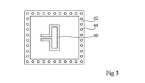
figure 3 est une vue de dessus d'un élément d'antenne ; et - la
figure 4 est une vue de dessus de l'ensemble d'un système émetteur/récepteur.
- the
figure 1 is a simplified sectional view of a portion of an integrated transceiver system; - the
figure 2 is a simplified sectional view of an antenna part of the transmitter / receiver system of thefigure 1 ; - the
figure 3 is a top view of an antenna element; and - the
figure 4 is a top view of the entire transceiver system.
Par souci de clarté, de mêmes éléments ont été désignés par de mêmes références dans les différentes figures et, de plus, comme cela est habituel dans la représentation des circuits intégrés, les diverses figures ne sont pas tracées à l'échelle.For the sake of clarity, the same elements have been designated by the same references in the various figures and, moreover, as is customary in the representation of the integrated circuits, the various figures are not drawn to scale.
La
La puce 1 est montée sur une plaque d'interposeur 3. Cette plaque est surmontée d'un réseau d'interconnexions non représenté comprenant des couches isolantes, des pistes métalliques sur un niveau ou plus, et des vias. Le montage de la puce 1 sur la plaque d'interposeur 3 est effectué par exemple par l'intermédiaire de piliers conducteurs 5, par exemple en cuivre.The
Dans l'interposeur 3, qui est par exemple une plaquette de silicium ou de verre, sont formés des vias traversants isolés 8 dont un seul est représenté, qui sont reliés par le réseau d'interconnexions à des plots de la puce 1. Du côté inférieur de la plaque d'interposeur sont formées des métallisations 20 comprenant en fait en pratique un ensemble de métallisations, auxquelles sont fixées (soudées) des billes 21.In the
Sur la face supérieure de la plaque d'interposeur 3, sont disposées des antennes 30 constituées de pistes conductrices selon toute configuration d'antenne convenable pour l'émission et/ou la réception d'ondes millimétriques. Bien qu'une seule antenne apparaisse dans la vue en coupe de la
Une antenne 30 émet, quand elle est excitée, un rayonnement haute fréquence, aussi bien vers le haut que vers le bas. Pour renforcer le rendement de l'antenne et éviter les rayonnements parasites, il convient de renvoyer vers le haut le faisceau que cette antenne envoie vers le bas. Pour cela, on prévoit de disposer sous des ensembles d'antennes un bloc 32 comprenant, en regard de chaque antenne 30, un évidement 34 revêtu d'une métallisation 36 dont le fond 38 constitue un réflecteur. Ce réflecteur doit être disposé à une distance verticale de l'ordre de λ/4 de l'antenne, λ étant la longueur d'onde du rayonnement. Bien entendu, cette distance λ/4 doit être calculée en tenant compte du fait que l'espace entre l'antenne et le réflecteur comprend l'épaisseur de la plaque d'interposeur, de constante diélectrique de l'ordre de 12 si cet interposeur est en silicium, et un espace d'air de constante diélectrique égale à 1, ainsi qu'éventuellement une faible épaisseur d'isolant entre l'antenne et l'interposeur. L'épaisseur de la plaque d'interposeur est connue avec précision et la hauteur de l'évidement dans le bloc 32 est également déterminée avec précision.An
A titre d'exemple numérique, pour un interposeur en silicium d'une épaisseur de 120 µm, la hauteur de l'évidement sera de 400 µm pour une fréquence de 60 GHz, ce qui conduit à une bande passante de fonctionnement de l'ordre de 13 GHz.As a numerical example, for a silicon interposer of a thickness of 120 microns, the height of the recess will be 400 microns for a frequency of 60 GHz, which leads to a bandwidth of operation of the order 13 GHz.
La
La
Ainsi, la puce 1, la plaque d'interposeur 3 et les billes 21 forment un ensemble prêt à être livré par un fabricant à un monteur de système qui monte l'ensemble susmentionné sur un autre dispositif électronique, par exemple une carte de circuit imprimé sur laquelle sont formées des métallisations adaptées à recevoir les billes 21. La face supérieure de cet ensemble est de préférence encapsulée dans un corps isolant, par exemple en résine, pour la protection du produit et éventuellement son marquage.Thus, the
Selon un avantage du système décrit ci-dessus, les connexions entre la puce et les antennes peuvent avoir des longueurs minimales et bien déterminées.According to an advantage of the system described above, the connections between the chip and the antennas may have minimum and well-defined lengths.
La
Cette vue de dessus montre bien que chacune des antennes est isolée des voisines et de l'environnement par le réseau de vias.This view from above shows that each of the antennas is isolated from neighbors and the environment by the network of vias.
Bien entendu, la présente invention est susceptible de diverses variantes qui apparaîtront à l'homme de l'art, notamment en ce qui concerne la forme des antennes. En outre, on n'a pas décrit en détail les divers niveaux de métallisation formés sur l'interposeur, et notamment les métallisations destinées à connecter le circuit intégré à chacune des antennes. En effet, il s'agit là de dispositions courantes. L'important est que toutes ces métallisations sont disposées sur une même face d'un interposeur et peuvent donc avoir une dimension minimale.Of course, the present invention is capable of various variants that will occur to those skilled in the art, in particular as regards the shape of the antennas. In addition, the various metallization levels formed on the interposer have not been described in detail, and in particular the metallizations intended to connect the integrated circuit to each of the antennas. Indeed, these are current provisions. The important thing is that all these metallizations are arranged on the same face of an interposer and can therefore have a minimum dimension.
Claims (6)
Applications Claiming Priority (1)
| Application Number | Priority Date | Filing Date | Title |
|---|---|---|---|
| FR1060849A FR2969397B1 (en) | 2010-12-20 | 2010-12-20 | INTEGRATED EMITTER-RECEIVER IN MILLIMETER WAVES |
Publications (2)
| Publication Number | Publication Date |
|---|---|
| EP2466687A1 true EP2466687A1 (en) | 2012-06-20 |
| EP2466687B1 EP2466687B1 (en) | 2015-11-25 |
Family
ID=44310135
Family Applications (1)
| Application Number | Title | Priority Date | Filing Date |
|---|---|---|---|
| EP11193822.1A Not-in-force EP2466687B1 (en) | 2010-12-20 | 2011-12-15 | Integral transceiver in millimetric waves |
Country Status (3)
| Country | Link |
|---|---|
| US (1) | US9070982B2 (en) |
| EP (1) | EP2466687B1 (en) |
| FR (1) | FR2969397B1 (en) |
Cited By (1)
| Publication number | Priority date | Publication date | Assignee | Title |
|---|---|---|---|---|
| CN111033890A (en) * | 2017-08-24 | 2020-04-17 | 高通股份有限公司 | Antenna arrangement on package |
Families Citing this family (6)
| Publication number | Priority date | Publication date | Assignee | Title |
|---|---|---|---|---|
| US9647329B2 (en) | 2014-04-09 | 2017-05-09 | Texas Instruments Incorporated | Encapsulated molded package with embedded antenna for high data rate communication using a dielectric waveguide |
| CN104465547B (en) * | 2014-12-10 | 2017-06-30 | 华进半导体封装先导技术研发中心有限公司 | The encapsulating structure and manufacture method of high frequency antenna signal reflex |
| US9941226B2 (en) | 2014-12-15 | 2018-04-10 | Industrial Technology Research Institute | Integrated millimeter-wave chip package |
| WO2017052656A1 (en) * | 2015-09-25 | 2017-03-30 | Intel Corporation | Microelectronic package communication using radio interfaces connected through waveguides |
| FR3071366B1 (en) * | 2017-09-18 | 2020-10-02 | Valeo Comfort & Driving Assistance | ANTENNA, ELECTRONIC MODULE AND COMMUNICATION KIT INCLUDING SUCH ANTENNA. |
| US11049824B2 (en) | 2019-10-17 | 2021-06-29 | Viasat, Inc. | Antenna apparatus with integrated antenna array and low loss multi-layer interposer |
Citations (4)
| Publication number | Priority date | Publication date | Assignee | Title |
|---|---|---|---|---|
| EP0476675A1 (en) * | 1990-09-20 | 1992-03-25 | Hughes Aircraft Company | Resonator-fed EHF distribution apparatus. |
| JP2001028413A (en) * | 1996-02-29 | 2001-01-30 | Kyocera Corp | Package for high-frequency waves |
| WO2005093902A1 (en) * | 2004-03-10 | 2005-10-06 | Raytheon Company | Cavity-backed antennas with dielectric and air cavities, and reflect-array antenna and millimeter-wave transmission system incorporating the same |
| KR100780328B1 (en) * | 2006-12-22 | 2007-11-28 | (주)텔콤코리아 | Array antenna for mobile communication |
Family Cites Families (13)
| Publication number | Priority date | Publication date | Assignee | Title |
|---|---|---|---|---|
| JP3308734B2 (en) | 1994-10-13 | 2002-07-29 | 本田技研工業株式会社 | Radar module |
| US5666128A (en) * | 1996-03-26 | 1997-09-09 | Lockheed Martin Corp. | Modular supertile array antenna |
| GB2356737A (en) | 1999-11-26 | 2001-05-30 | Nokia Mobile Phones Ltd | Ground Plane for a Semiconductor Chip |
| US7122891B2 (en) | 2003-12-23 | 2006-10-17 | Intel Corporation | Ceramic embedded wireless antenna |
| WO2005074029A1 (en) | 2004-01-28 | 2005-08-11 | Matsushita Electric Industrial Co., Ltd. | Module and mounting structure using the same |
| US7545323B2 (en) * | 2005-10-31 | 2009-06-09 | The Boeing Company | Phased array antenna systems and methods |
| US7741707B2 (en) | 2006-02-27 | 2010-06-22 | Stats Chippac Ltd. | Stackable integrated circuit package system |
| US7551136B1 (en) * | 2006-07-24 | 2009-06-23 | The Boeing Company | Multi-beam phased array antenna for limited scan applications |
| US7518229B2 (en) | 2006-08-03 | 2009-04-14 | International Business Machines Corporation | Versatile Si-based packaging with integrated passive components for mmWave applications |
| DE102006039279B4 (en) | 2006-08-22 | 2013-10-10 | Kathrein-Werke Kg | Dipole radiator arrangement |
| US8063846B2 (en) * | 2006-12-28 | 2011-11-22 | Sanyo Electric Co., Ltd. | Semiconductor module and mobile apparatus |
| US20100289713A1 (en) | 2007-05-16 | 2010-11-18 | Toru Taura | Slot antenna |
| US8013784B2 (en) | 2009-03-03 | 2011-09-06 | Toyota Motor Engineering & Manufacturing North America, Inc. | Butler matrix for 3D integrated RF front-ends |
-
2010
- 2010-12-20 FR FR1060849A patent/FR2969397B1/en not_active Expired - Fee Related
-
2011
- 2011-12-15 EP EP11193822.1A patent/EP2466687B1/en not_active Not-in-force
-
2012
- 2012-06-06 US US13/490,334 patent/US9070982B2/en active Active
Patent Citations (4)
| Publication number | Priority date | Publication date | Assignee | Title |
|---|---|---|---|---|
| EP0476675A1 (en) * | 1990-09-20 | 1992-03-25 | Hughes Aircraft Company | Resonator-fed EHF distribution apparatus. |
| JP2001028413A (en) * | 1996-02-29 | 2001-01-30 | Kyocera Corp | Package for high-frequency waves |
| WO2005093902A1 (en) * | 2004-03-10 | 2005-10-06 | Raytheon Company | Cavity-backed antennas with dielectric and air cavities, and reflect-array antenna and millimeter-wave transmission system incorporating the same |
| KR100780328B1 (en) * | 2006-12-22 | 2007-11-28 | (주)텔콤코리아 | Array antenna for mobile communication |
Cited By (2)
| Publication number | Priority date | Publication date | Assignee | Title |
|---|---|---|---|---|
| CN111033890A (en) * | 2017-08-24 | 2020-04-17 | 高通股份有限公司 | Antenna arrangement on package |
| CN111033890B (en) * | 2017-08-24 | 2023-04-28 | 高通股份有限公司 | Antenna arrangement on package |
Also Published As
| Publication number | Publication date |
|---|---|
| US20130027274A1 (en) | 2013-01-31 |
| FR2969397A1 (en) | 2012-06-22 |
| FR2969397B1 (en) | 2013-09-06 |
| EP2466687B1 (en) | 2015-11-25 |
| US9070982B2 (en) | 2015-06-30 |
Similar Documents
| Publication | Publication Date | Title |
|---|---|---|
| EP2466687B1 (en) | Integral transceiver in millimetric waves | |
| FR2969398A1 (en) | INTEGRATED EMITTER-RECEIVER IN MILLIMETER WAVES | |
| EP3057130B1 (en) | Rf transmission device with built-in electromagnetic wave reflector | |
| EP2429027B1 (en) | Coupler within a housing | |
| EP0307338B1 (en) | Microwave plate antenna, especially for a Doppler radar | |
| US9490220B2 (en) | Redistribution structures for microfeature workpieces | |
| FR2849927A1 (en) | RADAR TRANSCEIVER FOR MICROWAVE AND MILLIMETER WAVE APPLICATIONS | |
| EP0012055A1 (en) | Microstrip monopulse primary feed and antenna using same | |
| FR2952240A1 (en) | DIELECTRIC RESONATOR ANTENNA WITH DOUBLE POLARIZATION | |
| FR2865041A1 (en) | INTEGRATED CIRCUIT FOR MEASURING DISTANCE AND / OR SPEED OF OBJECTS | |
| FR2990314A1 (en) | MICROELECTRONIC DEVICE FOR WIRELESS TRANSMISSION | |
| EP1657749B1 (en) | Multilevel microelectronic package with internal shielding | |
| WO1998057391A1 (en) | Integrated transmitter or receiver device | |
| WO2012095365A1 (en) | Dielectric resonator antenna | |
| FR2629271A1 (en) | DEVICE FOR INTERCONNECTING AND PROTECTING A BULK MICROFREQUENCY COMPONENT BLEACH | |
| EP3840116B1 (en) | Reconfigurable antenna with transmitter network with monolithic integration of elementary cells | |
| FR3127642A1 (en) | Integrated waveguide microcircuit | |
| FR2847726A1 (en) | Radio frequency module for communication module, has dielectric substrate whose thickness and nature are selected by holding account of surface of conductive layer and stock points, to couple another layer to earth by capacitor | |
| FR3096837A1 (en) | Electronic device comprising an integrated electromagnetic antenna | |
| EP2323077A1 (en) | Electronic device including a semi-conductor component integrating an antenna. | |
| EP3537541B1 (en) | Electromagnetic decoupling | |
| CA2920445A1 (en) | Device for transmitting and/or receiving radiofrequency signals | |
| EP3537540B1 (en) | Electromagnetic decoupling | |
| EP4099498A1 (en) | Stack for manufacturing an integrated circuit intended for providing an electromagnetic lens function for a reconfigurable antenna with transmitter network | |
| FR3133480A1 (en) | Electronic device |
Legal Events
| Date | Code | Title | Description |
|---|---|---|---|
| PUAI | Public reference made under article 153(3) epc to a published international application that has entered the european phase |
Free format text: ORIGINAL CODE: 0009012 |
|
| AK | Designated contracting states |
Kind code of ref document: A1 Designated state(s): AL AT BE BG CH CY CZ DE DK EE ES FI FR GB GR HR HU IE IS IT LI LT LU LV MC MK MT NL NO PL PT RO RS SE SI SK SM TR |
|
| AX | Request for extension of the european patent |
Extension state: BA ME |
|
| 17P | Request for examination filed |
Effective date: 20120803 |
|
| GRAP | Despatch of communication of intention to grant a patent |
Free format text: ORIGINAL CODE: EPIDOSNIGR1 |
|
| INTG | Intention to grant announced |
Effective date: 20150703 |
|
| RIC1 | Information provided on ipc code assigned before grant |
Ipc: H01Q 13/18 20060101AFI20150619BHEP Ipc: H01Q 23/00 20060101ALI20150619BHEP Ipc: H01Q 21/06 20060101ALN20150619BHEP |
|
| GRAS | Grant fee paid |
Free format text: ORIGINAL CODE: EPIDOSNIGR3 |
|
| GRAA | (expected) grant |
Free format text: ORIGINAL CODE: 0009210 |
|
| AK | Designated contracting states |
Kind code of ref document: B1 Designated state(s): AL AT BE BG CH CY CZ DE DK EE ES FI FR GB GR HR HU IE IS IT LI LT LU LV MC MK MT NL NO PL PT RO RS SE SI SK SM TR |
|
| REG | Reference to a national code |
Ref country code: GB Ref legal event code: FG4D Free format text: NOT ENGLISH |
|
| REG | Reference to a national code |
Ref country code: CH Ref legal event code: EP |
|
| REG | Reference to a national code |
Ref country code: AT Ref legal event code: REF Ref document number: 763015 Country of ref document: AT Kind code of ref document: T Effective date: 20151215 |
|
| REG | Reference to a national code |
Ref country code: IE Ref legal event code: FG4D Free format text: LANGUAGE OF EP DOCUMENT: FRENCH |
|
| REG | Reference to a national code |
Ref country code: FR Ref legal event code: PLFP Year of fee payment: 5 |
|
| REG | Reference to a national code |
Ref country code: DE Ref legal event code: R096 Ref document number: 602011021586 Country of ref document: DE |
|
| REG | Reference to a national code |
Ref country code: LT Ref legal event code: MG4D |
|
| REG | Reference to a national code |
Ref country code: NL Ref legal event code: MP Effective date: 20160225 |
|
| REG | Reference to a national code |
Ref country code: AT Ref legal event code: MK05 Ref document number: 763015 Country of ref document: AT Kind code of ref document: T Effective date: 20151125 |
|
| PG25 | Lapsed in a contracting state [announced via postgrant information from national office to epo] |
Ref country code: ES Free format text: LAPSE BECAUSE OF FAILURE TO SUBMIT A TRANSLATION OF THE DESCRIPTION OR TO PAY THE FEE WITHIN THE PRESCRIBED TIME-LIMIT Effective date: 20151125 Ref country code: IS Free format text: LAPSE BECAUSE OF FAILURE TO SUBMIT A TRANSLATION OF THE DESCRIPTION OR TO PAY THE FEE WITHIN THE PRESCRIBED TIME-LIMIT Effective date: 20160325 Ref country code: LT Free format text: LAPSE BECAUSE OF FAILURE TO SUBMIT A TRANSLATION OF THE DESCRIPTION OR TO PAY THE FEE WITHIN THE PRESCRIBED TIME-LIMIT Effective date: 20151125 Ref country code: NL Free format text: LAPSE BECAUSE OF FAILURE TO SUBMIT A TRANSLATION OF THE DESCRIPTION OR TO PAY THE FEE WITHIN THE PRESCRIBED TIME-LIMIT Effective date: 20151125 Ref country code: NO Free format text: LAPSE BECAUSE OF FAILURE TO SUBMIT A TRANSLATION OF THE DESCRIPTION OR TO PAY THE FEE WITHIN THE PRESCRIBED TIME-LIMIT Effective date: 20160225 Ref country code: HR Free format text: LAPSE BECAUSE OF FAILURE TO SUBMIT A TRANSLATION OF THE DESCRIPTION OR TO PAY THE FEE WITHIN THE PRESCRIBED TIME-LIMIT Effective date: 20151125 |
|
| PG25 | Lapsed in a contracting state [announced via postgrant information from national office to epo] |
Ref country code: RS Free format text: LAPSE BECAUSE OF FAILURE TO SUBMIT A TRANSLATION OF THE DESCRIPTION OR TO PAY THE FEE WITHIN THE PRESCRIBED TIME-LIMIT Effective date: 20151125 Ref country code: AT Free format text: LAPSE BECAUSE OF FAILURE TO SUBMIT A TRANSLATION OF THE DESCRIPTION OR TO PAY THE FEE WITHIN THE PRESCRIBED TIME-LIMIT Effective date: 20151125 Ref country code: FI Free format text: LAPSE BECAUSE OF FAILURE TO SUBMIT A TRANSLATION OF THE DESCRIPTION OR TO PAY THE FEE WITHIN THE PRESCRIBED TIME-LIMIT Effective date: 20151125 Ref country code: LV Free format text: LAPSE BECAUSE OF FAILURE TO SUBMIT A TRANSLATION OF THE DESCRIPTION OR TO PAY THE FEE WITHIN THE PRESCRIBED TIME-LIMIT Effective date: 20151125 Ref country code: PT Free format text: LAPSE BECAUSE OF FAILURE TO SUBMIT A TRANSLATION OF THE DESCRIPTION OR TO PAY THE FEE WITHIN THE PRESCRIBED TIME-LIMIT Effective date: 20160325 Ref country code: PL Free format text: LAPSE BECAUSE OF FAILURE TO SUBMIT A TRANSLATION OF THE DESCRIPTION OR TO PAY THE FEE WITHIN THE PRESCRIBED TIME-LIMIT Effective date: 20151125 Ref country code: SE Free format text: LAPSE BECAUSE OF FAILURE TO SUBMIT A TRANSLATION OF THE DESCRIPTION OR TO PAY THE FEE WITHIN THE PRESCRIBED TIME-LIMIT Effective date: 20151125 Ref country code: GR Free format text: LAPSE BECAUSE OF FAILURE TO SUBMIT A TRANSLATION OF THE DESCRIPTION OR TO PAY THE FEE WITHIN THE PRESCRIBED TIME-LIMIT Effective date: 20160226 Ref country code: BE Free format text: LAPSE BECAUSE OF NON-PAYMENT OF DUE FEES Effective date: 20151231 |
|
| PG25 | Lapsed in a contracting state [announced via postgrant information from national office to epo] |
Ref country code: CZ Free format text: LAPSE BECAUSE OF FAILURE TO SUBMIT A TRANSLATION OF THE DESCRIPTION OR TO PAY THE FEE WITHIN THE PRESCRIBED TIME-LIMIT Effective date: 20151125 Ref country code: IT Free format text: LAPSE BECAUSE OF FAILURE TO SUBMIT A TRANSLATION OF THE DESCRIPTION OR TO PAY THE FEE WITHIN THE PRESCRIBED TIME-LIMIT Effective date: 20151125 |
|
| REG | Reference to a national code |
Ref country code: CH Ref legal event code: PL |
|
| REG | Reference to a national code |
Ref country code: DE Ref legal event code: R097 Ref document number: 602011021586 Country of ref document: DE |
|
| PG25 | Lapsed in a contracting state [announced via postgrant information from national office to epo] |
Ref country code: EE Free format text: LAPSE BECAUSE OF FAILURE TO SUBMIT A TRANSLATION OF THE DESCRIPTION OR TO PAY THE FEE WITHIN THE PRESCRIBED TIME-LIMIT Effective date: 20151125 Ref country code: SK Free format text: LAPSE BECAUSE OF FAILURE TO SUBMIT A TRANSLATION OF THE DESCRIPTION OR TO PAY THE FEE WITHIN THE PRESCRIBED TIME-LIMIT Effective date: 20151125 Ref country code: RO Free format text: LAPSE BECAUSE OF FAILURE TO SUBMIT A TRANSLATION OF THE DESCRIPTION OR TO PAY THE FEE WITHIN THE PRESCRIBED TIME-LIMIT Effective date: 20151125 Ref country code: DK Free format text: LAPSE BECAUSE OF FAILURE TO SUBMIT A TRANSLATION OF THE DESCRIPTION OR TO PAY THE FEE WITHIN THE PRESCRIBED TIME-LIMIT Effective date: 20151125 Ref country code: SM Free format text: LAPSE BECAUSE OF FAILURE TO SUBMIT A TRANSLATION OF THE DESCRIPTION OR TO PAY THE FEE WITHIN THE PRESCRIBED TIME-LIMIT Effective date: 20151125 |
|
| REG | Reference to a national code |
Ref country code: IE Ref legal event code: MM4A |
|
| PG25 | Lapsed in a contracting state [announced via postgrant information from national office to epo] |
Ref country code: MC Free format text: LAPSE BECAUSE OF FAILURE TO SUBMIT A TRANSLATION OF THE DESCRIPTION OR TO PAY THE FEE WITHIN THE PRESCRIBED TIME-LIMIT Effective date: 20151125 |
|
| PLBE | No opposition filed within time limit |
Free format text: ORIGINAL CODE: 0009261 |
|
| STAA | Information on the status of an ep patent application or granted ep patent |
Free format text: STATUS: NO OPPOSITION FILED WITHIN TIME LIMIT |
|
| PG25 | Lapsed in a contracting state [announced via postgrant information from national office to epo] |
Ref country code: LI Free format text: LAPSE BECAUSE OF NON-PAYMENT OF DUE FEES Effective date: 20151231 Ref country code: CH Free format text: LAPSE BECAUSE OF NON-PAYMENT OF DUE FEES Effective date: 20151231 Ref country code: IE Free format text: LAPSE BECAUSE OF NON-PAYMENT OF DUE FEES Effective date: 20151215 |
|
| 26N | No opposition filed |
Effective date: 20160826 |
|
| PG25 | Lapsed in a contracting state [announced via postgrant information from national office to epo] |
Ref country code: SI Free format text: LAPSE BECAUSE OF FAILURE TO SUBMIT A TRANSLATION OF THE DESCRIPTION OR TO PAY THE FEE WITHIN THE PRESCRIBED TIME-LIMIT Effective date: 20151125 |
|
| REG | Reference to a national code |
Ref country code: FR Ref legal event code: PLFP Year of fee payment: 6 |
|
| PGFP | Annual fee paid to national office [announced via postgrant information from national office to epo] |
Ref country code: GB Payment date: 20161221 Year of fee payment: 6 |
|
| PGFP | Annual fee paid to national office [announced via postgrant information from national office to epo] |
Ref country code: FR Payment date: 20161229 Year of fee payment: 6 |
|
| PGFP | Annual fee paid to national office [announced via postgrant information from national office to epo] |
Ref country code: DE Payment date: 20161221 Year of fee payment: 6 |
|
| PG25 | Lapsed in a contracting state [announced via postgrant information from national office to epo] |
Ref country code: BG Free format text: LAPSE BECAUSE OF FAILURE TO SUBMIT A TRANSLATION OF THE DESCRIPTION OR TO PAY THE FEE WITHIN THE PRESCRIBED TIME-LIMIT Effective date: 20151125 Ref country code: HU Free format text: LAPSE BECAUSE OF FAILURE TO SUBMIT A TRANSLATION OF THE DESCRIPTION OR TO PAY THE FEE WITHIN THE PRESCRIBED TIME-LIMIT; INVALID AB INITIO Effective date: 20111215 |
|
| PG25 | Lapsed in a contracting state [announced via postgrant information from national office to epo] |
Ref country code: CY Free format text: LAPSE BECAUSE OF FAILURE TO SUBMIT A TRANSLATION OF THE DESCRIPTION OR TO PAY THE FEE WITHIN THE PRESCRIBED TIME-LIMIT Effective date: 20151125 |
|
| PG25 | Lapsed in a contracting state [announced via postgrant information from national office to epo] |
Ref country code: MT Free format text: LAPSE BECAUSE OF FAILURE TO SUBMIT A TRANSLATION OF THE DESCRIPTION OR TO PAY THE FEE WITHIN THE PRESCRIBED TIME-LIMIT Effective date: 20151125 Ref country code: TR Free format text: LAPSE BECAUSE OF FAILURE TO SUBMIT A TRANSLATION OF THE DESCRIPTION OR TO PAY THE FEE WITHIN THE PRESCRIBED TIME-LIMIT Effective date: 20151125 |
|
| PG25 | Lapsed in a contracting state [announced via postgrant information from national office to epo] |
Ref country code: LU Free format text: LAPSE BECAUSE OF NON-PAYMENT OF DUE FEES Effective date: 20151215 |
|
| PG25 | Lapsed in a contracting state [announced via postgrant information from national office to epo] |
Ref country code: MK Free format text: LAPSE BECAUSE OF FAILURE TO SUBMIT A TRANSLATION OF THE DESCRIPTION OR TO PAY THE FEE WITHIN THE PRESCRIBED TIME-LIMIT Effective date: 20151125 |
|
| REG | Reference to a national code |
Ref country code: DE Ref legal event code: R119 Ref document number: 602011021586 Country of ref document: DE |
|
| GBPC | Gb: european patent ceased through non-payment of renewal fee |
Effective date: 20171215 |
|
| REG | Reference to a national code |
Ref country code: FR Ref legal event code: ST Effective date: 20180831 |
|
| PG25 | Lapsed in a contracting state [announced via postgrant information from national office to epo] |
Ref country code: DE Free format text: LAPSE BECAUSE OF NON-PAYMENT OF DUE FEES Effective date: 20180703 Ref country code: AL Free format text: LAPSE BECAUSE OF FAILURE TO SUBMIT A TRANSLATION OF THE DESCRIPTION OR TO PAY THE FEE WITHIN THE PRESCRIBED TIME-LIMIT Effective date: 20151125 Ref country code: FR Free format text: LAPSE BECAUSE OF NON-PAYMENT OF DUE FEES Effective date: 20180102 |
|
| PG25 | Lapsed in a contracting state [announced via postgrant information from national office to epo] |
Ref country code: GB Free format text: LAPSE BECAUSE OF NON-PAYMENT OF DUE FEES Effective date: 20171215 |