EP2463897B1 - Integrating n-type and p-type metal gate field effect transistors - Google Patents
Integrating n-type and p-type metal gate field effect transistors Download PDFInfo
- Publication number
- EP2463897B1 EP2463897B1 EP12158444.5A EP12158444A EP2463897B1 EP 2463897 B1 EP2463897 B1 EP 2463897B1 EP 12158444 A EP12158444 A EP 12158444A EP 2463897 B1 EP2463897 B1 EP 2463897B1
- Authority
- EP
- European Patent Office
- Prior art keywords
- type
- gate
- polysilicon
- trench
- type metal
- Prior art date
- Legal status (The legal status is an assumption and is not a legal conclusion. Google has not performed a legal analysis and makes no representation as to the accuracy of the status listed.)
- Expired - Lifetime
Links
Images


Classifications
-
- H—ELECTRICITY
- H10—SEMICONDUCTOR DEVICES; ELECTRIC SOLID-STATE DEVICES NOT OTHERWISE PROVIDED FOR
- H10D—INORGANIC ELECTRIC SEMICONDUCTOR DEVICES
- H10D64/00—Electrodes of devices having potential barriers
- H10D64/01—Manufacture or treatment
- H10D64/017—Manufacture or treatment using dummy gates in processes wherein at least parts of the final gates are self-aligned to the dummy gates, i.e. replacement gate processes
-
- H—ELECTRICITY
- H10—SEMICONDUCTOR DEVICES; ELECTRIC SOLID-STATE DEVICES NOT OTHERWISE PROVIDED FOR
- H10D—INORGANIC ELECTRIC SEMICONDUCTOR DEVICES
- H10D64/00—Electrodes of devices having potential barriers
- H10D64/60—Electrodes characterised by their materials
- H10D64/66—Electrodes having a conductor capacitively coupled to a semiconductor by an insulator, e.g. MIS electrodes
- H10D64/665—Electrodes having a conductor capacitively coupled to a semiconductor by an insulator, e.g. MIS electrodes the conductor comprising a layer of elemental metal contacting the insulator, e.g. tungsten or molybdenum
-
- H—ELECTRICITY
- H10—SEMICONDUCTOR DEVICES; ELECTRIC SOLID-STATE DEVICES NOT OTHERWISE PROVIDED FOR
- H10D—INORGANIC ELECTRIC SEMICONDUCTOR DEVICES
- H10D64/00—Electrodes of devices having potential barriers
- H10D64/60—Electrodes characterised by their materials
- H10D64/66—Electrodes having a conductor capacitively coupled to a semiconductor by an insulator, e.g. MIS electrodes
- H10D64/667—Electrodes having a conductor capacitively coupled to a semiconductor by an insulator, e.g. MIS electrodes the conductor comprising a layer of alloy material, compound material or organic material contacting the insulator, e.g. TiN workfunction layers
-
- H—ELECTRICITY
- H10—SEMICONDUCTOR DEVICES; ELECTRIC SOLID-STATE DEVICES NOT OTHERWISE PROVIDED FOR
- H10D—INORGANIC ELECTRIC SEMICONDUCTOR DEVICES
- H10D84/00—Integrated devices formed in or on semiconductor substrates that comprise only semiconducting layers, e.g. on Si wafers or on GaAs-on-Si wafers
- H10D84/01—Manufacture or treatment
- H10D84/0123—Integrating together multiple components covered by H10D12/00 or H10D30/00, e.g. integrating multiple IGBTs
- H10D84/0126—Integrating together multiple components covered by H10D12/00 or H10D30/00, e.g. integrating multiple IGBTs the components including insulated gates, e.g. IGFETs
- H10D84/0165—Integrating together multiple components covered by H10D12/00 or H10D30/00, e.g. integrating multiple IGBTs the components including insulated gates, e.g. IGFETs the components including complementary IGFETs, e.g. CMOS devices
- H10D84/0172—Manufacturing their gate conductors
- H10D84/0177—Manufacturing their gate conductors the gate conductors having different materials or different implants
-
- H—ELECTRICITY
- H10—SEMICONDUCTOR DEVICES; ELECTRIC SOLID-STATE DEVICES NOT OTHERWISE PROVIDED FOR
- H10D—INORGANIC ELECTRIC SEMICONDUCTOR DEVICES
- H10D84/00—Integrated devices formed in or on semiconductor substrates that comprise only semiconducting layers, e.g. on Si wafers or on GaAs-on-Si wafers
- H10D84/01—Manufacture or treatment
- H10D84/02—Manufacture or treatment characterised by using material-based technologies
- H10D84/03—Manufacture or treatment characterised by using material-based technologies using Group IV technology, e.g. silicon technology or silicon-carbide [SiC] technology
- H10D84/038—Manufacture or treatment characterised by using material-based technologies using Group IV technology, e.g. silicon technology or silicon-carbide [SiC] technology using silicon technology, e.g. SiGe
-
- H—ELECTRICITY
- H10—SEMICONDUCTOR DEVICES; ELECTRIC SOLID-STATE DEVICES NOT OTHERWISE PROVIDED FOR
- H10P—GENERIC PROCESSES OR APPARATUS FOR THE MANUFACTURE OR TREATMENT OF DEVICES COVERED BY CLASS H10
- H10P50/00—Etching of wafers, substrates or parts of devices
- H10P50/20—Dry etching; Plasma etching; Reactive-ion etching
- H10P50/26—Dry etching; Plasma etching; Reactive-ion etching of conductive or resistive materials
- H10P50/264—Dry etching; Plasma etching; Reactive-ion etching of conductive or resistive materials by chemical means
- H10P50/266—Dry etching; Plasma etching; Reactive-ion etching of conductive or resistive materials by chemical means by vapour etching only
- H10P50/267—Dry etching; Plasma etching; Reactive-ion etching of conductive or resistive materials by chemical means by vapour etching only using plasmas
- H10P50/268—Dry etching; Plasma etching; Reactive-ion etching of conductive or resistive materials by chemical means by vapour etching only using plasmas of silicon-containing layers
-
- H—ELECTRICITY
- H10—SEMICONDUCTOR DEVICES; ELECTRIC SOLID-STATE DEVICES NOT OTHERWISE PROVIDED FOR
- H10P—GENERIC PROCESSES OR APPARATUS FOR THE MANUFACTURE OR TREATMENT OF DEVICES COVERED BY CLASS H10
- H10P50/00—Etching of wafers, substrates or parts of devices
- H10P50/60—Wet etching
- H10P50/66—Wet etching of conductive or resistive materials
- H10P50/663—Wet etching of conductive or resistive materials by chemical means only
- H10P50/667—Wet etching of conductive or resistive materials by chemical means only by liquid etching only
-
- H—ELECTRICITY
- H10—SEMICONDUCTOR DEVICES; ELECTRIC SOLID-STATE DEVICES NOT OTHERWISE PROVIDED FOR
- H10D—INORGANIC ELECTRIC SEMICONDUCTOR DEVICES
- H10D30/00—Field-effect transistors [FET]
- H10D30/60—Insulated-gate field-effect transistors [IGFET]
- H10D30/601—Insulated-gate field-effect transistors [IGFET] having lightly-doped drain or source extensions, e.g. LDD IGFETs or DDD IGFETs
-
- Y—GENERAL TAGGING OF NEW TECHNOLOGICAL DEVELOPMENTS; GENERAL TAGGING OF CROSS-SECTIONAL TECHNOLOGIES SPANNING OVER SEVERAL SECTIONS OF THE IPC; TECHNICAL SUBJECTS COVERED BY FORMER USPC CROSS-REFERENCE ART COLLECTIONS [XRACs] AND DIGESTS
- Y10—TECHNICAL SUBJECTS COVERED BY FORMER USPC
- Y10S—TECHNICAL SUBJECTS COVERED BY FORMER USPC CROSS-REFERENCE ART COLLECTIONS [XRACs] AND DIGESTS
- Y10S438/00—Semiconductor device manufacturing: process
- Y10S438/926—Dummy metallization
Definitions
- Embodiments of the invention relate to the manufacturing of complementary metal-oxide-semiconductor (CMOS) devices. More particularly, embodiments of the invention relate to integrating n-type and p-type metal gate transistors within a single CMOS device.
- CMOS complementary metal-oxide-semiconductor
- CMOS devices manufactured with prior art semiconductor processes typically have polysilicon gate structures.
- Polysilicon can be susceptible to depletion effects, which can add to the overall gate dielectric thickness in the CMOS device. Furthermore, as the effective physical gate dielectric thickness decreases, the polysilicon depletion contributes proportionally to the total dielectric thickness. It is, therefore, desirable to eliminate polysilicon depletion in order to scale gate oxide thickness.
- Metal gates are not as susceptible to depletion as polysilicon and are in many ways preferable to polysilicon for forming gate structures.
- Typical prior art semiconductor processes do not incorporate n-type and p-type metal gates within the same device or integrated circuit. This is due, in part, to the complexity and cost of developing a semiconductor process that can reliably deposit metal gate structures of differing types into the same semiconductor device or integrated circuit.
- US 6,376,888 B1 discloses a semiconductor device and method of manufacturing the same.
- a resist layer is formed in an n-type MIS transistor region.
- Germanium ions (Ge + ) are selectively implanted into only the Tungsten silicide film in the p-type MIS transistor region using a resist layer as a mask so as to form a Tungsten silicide film containing Germanium.
- a resist layer is formed in the p-type MIS transistor region.
- Indium ions (In + ) are selectively implanted into only the Tungsten silicide film in the n-type MIS transistor region by using the resist layer as a mask so as to form a Tungsten silicide film containing Indium.
- GB 2 358 737 A discloses methods for manufacturing a complementary MOSFET device.
- dummy gate electrodes are deposited on a substrate that are used as ion implantation masks and then an insulation film is formed over the substrate and dummy gate electrodes are formed. The dummy electrodes are removed separately and the recesses left in the insulation film are individually filled with different gate electrode materials.
- gate electrodes are separately formed of different materials in recesses formed in an insulation layer and then these actual electrodes are used as implantation masks.
- CMOS complementary metal-oxide-semiconductor
- CMOS devices and integrated circuits that can avoid the effects of gate depletion
- embodiments incorporate n-type and p-type metal gates into the same CMOS device or integrated circuits.
- Figure 1 illustrates a cross-section of a CMOS device containing a p-type transistor and an n-type transistor after depositing ILD0 ("Inter-layer dielectric") according to one embodiment.
- poly-silicon gate transistors 105, 110 are fabricated using standard CMOS processing techniques in order to prevent silicide formation on the poly-silicon gate electrode.
- the nitride hard masks 115 are to protect the gate structures during silicidation and ILD0 120 is deposited on the structure.
- the ILD0 is polished back to expose the doped polysilicon gates in Figure 2 .
- the ILD0 polishing also removes residual silicide around the nitride masking layer.
- an ammonium hydroxide etch is used to selectively etch away 305 the n-type polysilicon.
- the ammonium hydroxide etch is low temperature (e.g., ⁇ 40 deg. Celsius), uses sonication, and has a concentration of approximately 2 - 29%.
- the result of the polysilicon etch is illustrated in Figure 3 .
- n-type metal 405 such as Hf, Zr, Ti, Ta, or Al
- the trench can be filled with an alloy containing an n-type component using PVD ("Physical vapor deposition"), CVD ("Chemical vapor deposition"), or ALD ("Atomic Layer deposition”).
- PVD Physical vapor deposition
- CVD Chemical vapor deposition
- ALD Atomic Layer deposition
- CVD and ALD may use an organometallic or halide precursor, and a reducing atmosphere.
- the thickness of the n-type metal or alloy can be such that the trench is only partially filled.
- the thickness of the n-type metal or alloy can vary from approximately 50 angstroms to approximately 1000 angstroms in various embodiments. If the trenches are not completely filled, they may be filled with an easily polished metal, such as W ("Tungsten") or Al ("Aluminum").
- the n-type metal gate can be doped by implanting n-type material after the metal gate have been deposited in the trench.
- the n-type metal is polished back to create the n-type metal gates 505 and to expose the p-type polysilicon gate 510 as illustrated in Figure 5 .
- Figure 6 illustrates in an alternative not forming part of the present invention the transistors after a selective dry etch is performed to remove the p-type polysilicon without removing the n-type metal gate.
- the selective dry etch can be performed using a parallel plate or ECR ("Electron cyclotron resonance") etcher and SF6 ("Sulfur hexafluoride"), HBr ("Hydrogen Bromide"), HI ("Hydrogen Iodide”), CI2 ("Chlorine”), Ar (“Argon”), and/or He (“Helium”).
- a wet etch such as approximately 20 - 30 % TMAH ("Tetramethylammonium Hydroxide") at approximately 60 - 90 degrees Celsius with or without sonication may also be used to remove the p-type polysilicon gate.
- TMAH Tetramethylammonium Hydroxide
- a p-type metal such as Ru (“Ruthenium”), Pd (“Palladium”), Pt ("Platinum”), Co (“Cobalt”), Ni (“Nickel”), TiAlN (“Titanium Aluminum Nitride”), or WCN (“Tungsten Carbon Nitride”) can be used to fill the gate trench created by etching the p-type polysilicon gate 510.
- an alloy using p-type metal can be deposited in the trench using chemical vapor deposition or atomic layer deposition with an organometallic precursor and a reducing atmosphere.
- the type metal gate can be doped by implanting the metal gate with p-type material after the metal gate has been deposited in the gate trench.
- the thickness of the p-type metal or alloy can be such that the trench is only partially filled.
- Figure 7 illustrates the transistors after the p-type metal or alloy has been deposited in the gate trench 710.
- the p-type metal or alloy is polished back, as illustrated in Figure 8 , to create the n-type and p-type gate structures 805, 810, and ILD0 is again deposited to provide room for the contact layer.
- Contacts 903 are etched and deposited, as illustrated in Figure 9 , resulting in the final transistor structure.
- the p-type polysilicon gate is converted to n-type in order to allow a gentler wet etch to remove the polysilicon rather than a dry etch.
- an n-type implant 1015 is performed to change the doping of the polysilicon in order to allow an ammonium hydroxide etch to be performed, as illustrated in Figure 10 .
- FIG. 11 The result of the implant and ash (if required) is illustrated in Figure 11 .
- An ammonium hydroxide etch removes the remaining polysilicon gate structure 1210 resulting in the structure illustrated in Figure 12 .
- a p-type metal or alloy is then deposited in the trench left by removing the p-type polysilicon gate as described above.
Landscapes
- Metal-Oxide And Bipolar Metal-Oxide Semiconductor Integrated Circuits (AREA)
- Electrodes Of Semiconductors (AREA)
Description
- Embodiments of the invention relate to the manufacturing of complementary metal-oxide-semiconductor (CMOS) devices. More particularly, embodiments of the invention relate to integrating n-type and p-type metal gate transistors within a single CMOS device.
- Prior art CMOS devices manufactured with prior art semiconductor processes typically have polysilicon gate structures. Polysilicon, however, can be susceptible to depletion effects, which can add to the overall gate dielectric thickness in the CMOS device. Furthermore, as the effective physical gate dielectric thickness decreases, the polysilicon depletion contributes proportionally to the total dielectric thickness. It is, therefore, desirable to eliminate polysilicon depletion in order to scale gate oxide thickness.
- Metal gates, on the other hand, are not as susceptible to depletion as polysilicon and are in many ways preferable to polysilicon for forming gate structures. Typical prior art semiconductor processes, however, do not incorporate n-type and p-type metal gates within the same device or integrated circuit. This is due, in part, to the complexity and cost of developing a semiconductor process that can reliably deposit metal gate structures of differing types into the same semiconductor device or integrated circuit.
-
US 6,376,888 B1 discloses a semiconductor device and method of manufacturing the same.A resist layer is formed in an n-type MIS transistor region. Then, Germanium ions (Ge+) are selectively implanted into only the Tungsten silicide film in the p-type MIS transistor region using a resist layer as a mask so as to form a Tungsten silicide film containing Germanium. Furthermore, in a next step, a resist layer is formed in the p-type MIS transistor region. Then, Indium ions (In+) are selectively implanted into only the Tungsten silicide film in the n-type MIS transistor region by using the resist layer as a mask so as to form a Tungsten silicide film containing Indium. -
GB 2 358 737 A - Embodiments of the invention are illustrated by way of example and not limitation in the figures of the accompanying drawings, in which like references indicate similar elements and in which:
-
Figure 1 illustrates the state of transistors after depositing ILD0 according to one embodiment. -
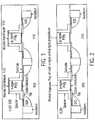
Figure 2 illustrates the state of transistors after ILD0 polish-back to expose polysilicon gate structures according to one embodiment. -
Figure 3 illustrates the state of transistors after selective n-type poly etch according to one embodiment. -
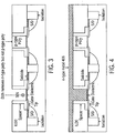
Figure 4 illustrates the state of transistors after depositing n-type metal according to one embodiment. -
Figure 5 illustrates the state of transistors after polishing the n-type metal according to one embodiment. -
Figure 6 illustrates the state of transistors after selectively etching p-type polysilicon according to one non-claimed embodiment. -
Figure 7 illustrates the state of transistors after depositing p-type metal according to one embodiment. -
Figure 8 illustrates the state of transistors after polishing the p-type metal according to one embodiment. -
Figure 9 illustrates the completed transistors according to one embodiment. -
Figure 10 illustrates the state of transistors after an implant patterning according to the present invention. -
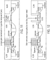
Figure 11 illustrates the state of transistors after n-type implant and ash. -
Figure 12 illustrates the state of transistors after a second selective n-type polysilicon etch. - The present invention is defined in the appended claims. More particularly, the present invention relates to the alternative embodiment disclosed with reference to
figures 10-12 , whereby the other alternative disclosed infigure 6 does not form part of the present invention. Embodiments of the invention described herein relate to semiconductor manufacturing. More particularly, embodiments of the invention described relate to integrating n-type and p-type metal gate transistors within the same complementary metal-oxide-semiconductor (CMOS) device or integrated circuit. - In order to manufacture CMOS devices and integrated circuits that can avoid the effects of gate depletion, embodiments incorporate n-type and p-type metal gates into the same CMOS device or integrated circuits.
-
Figure 1 illustrates a cross-section of a CMOS device containing a p-type transistor and an n-type transistor after depositing ILD0 ("Inter-layer dielectric") according to one embodiment. InFigure 1 , poly-silicon gate transistors hard masks 115 are to protect the gate structures during silicidation and ILD0 120 is deposited on the structure. - The ILD0 is polished back to expose the doped polysilicon gates in
Figure 2 . The ILD0 polishing also removes residual silicide around the nitride masking layer. After thepolysilicon gates Figure 3 . - Removal of the n-type polysilicon above the gate dielectric creates a damascene-like "trench" which is filled with an n-
type metal 405, such as Hf, Zr, Ti, Ta, or Al, as illustrated inFigure 4 . Alternatively, the trench can be filled with an alloy containing an n-type component using PVD ("Physical vapor deposition"), CVD ("Chemical vapor deposition"), or ALD ("Atomic Layer deposition"). CVD and ALD may use an organometallic or halide precursor, and a reducing atmosphere. Furthermore, the thickness of the n-type metal or alloy can be such that the trench is only partially filled. For example, the thickness of the n-type metal or alloy can vary from approximately 50 angstroms to approximately 1000 angstroms in various embodiments. If the trenches are not completely filled, they may be filled with an easily polished metal, such as W ("Tungsten") or Al ("Aluminum"). The n-type metal gate can be doped by implanting n-type material after the metal gate have been deposited in the trench. - The n-type metal is polished back to create the n-
type metal gates 505 and to expose the p-type polysilicon gate 510 as illustrated inFigure 5 . -
Figure 6 illustrates in an alternative not forming part of the present invention the transistors after a selective dry etch is performed to remove the p-type polysilicon without removing the n-type metal gate. The selective dry etch can be performed using a parallel plate or ECR ("Electron cyclotron resonance") etcher and SF6 ("Sulfur hexafluoride"), HBr ("Hydrogen Bromide"), HI ("Hydrogen Iodide"), CI2 ("Chlorine"), Ar ("Argon"), and/or He ("Helium"). Alternatively, a wet etch, such as approximately 20 - 30 % TMAH ("Tetramethylammonium Hydroxide") at approximately 60 - 90 degrees Celsius with or without sonication may also be used to remove the p-type polysilicon gate. - A p-type metal, such as Ru ("Ruthenium"), Pd ("Palladium"), Pt ("Platinum"), Co ("Cobalt"), Ni ("Nickel"), TiAlN ("Titanium Aluminum Nitride"), or WCN ("Tungsten Carbon Nitride") can be used to fill the gate trench created by etching the p-
type polysilicon gate 510. Alternatively, an alloy using p-type metal can be deposited in the trench using chemical vapor deposition or atomic layer deposition with an organometallic precursor and a reducing atmosphere. The type metal gate can be doped by implanting the metal gate with p-type material after the metal gate has been deposited in the gate trench. Furthermore, the thickness of the p-type metal or alloy can be such that the trench is only partially filled.Figure 7 illustrates the transistors after the p-type metal or alloy has been deposited in thegate trench 710. - The p-type metal or alloy is polished back, as illustrated in
Figure 8 , to create the n-type and p-type gate structures -
Contacts 903 are etched and deposited, as illustrated inFigure 9 , resulting in the final transistor structure. - According to the present invention, rather than using a dry etch to remove the p-type polysilicon as described above, the p-type polysilicon gate is converted to n-type in order to allow a gentler wet etch to remove the polysilicon rather than a dry etch. For example, after the p-
type polysilicon 1010 has been exposed, rather than using a selective dry etch to remove the polysilicon, an n-type implant 1015 is performed to change the doping of the polysilicon in order to allow an ammonium hydroxide etch to be performed, as illustrated inFigure 10 . - The result of the implant and ash (if required) is illustrated in
Figure 11 . An ammonium hydroxide etch removes the remainingpolysilicon gate structure 1210 resulting in the structure illustrated inFigure 12 . A p-type metal or alloy is then deposited in the trench left by removing the p-type polysilicon gate as described above.
Claims (5)
- A process of forming n-type and p-type metal gate transistors within a single CMOS device upon a semiconductor substrate, the process comprising forming the n-type and the p-type transistor comprising an n-type (205) and a p-type (210) polysilicon gate, respectively; removing an interlayer dielectric (ILD) layer from the top of the polysilicon gates to expose the polysilicon gates;
selectively etching away (305) the n-type polysilicon gate from amongst the exposed n-type and p-type polysilicon gates to form a first trench bound in part by substantially vertical lateral side-wall spacers and a gate dielectric on the bottom of the first trench;
depositing n-type metal (405) into the first trench;
removing excess n-type metal to expose the top of the n-type metal gate and the p-type polysilicon gate;
performing an n-type implant (1015) into the p-type polysilicon gate (210) in order to convert the p-type polysilicon gate into an n-type polysilicon gate;
selectively wet etching the n-type polysilicon gate from amongst the exposed n-type metal gate and the exposed n-type polysilicon gate to form a second trench bound in part by substantially vertical lateral side-wall spacers and a gate dielectric on the bottom of the second trench; depositing a p-type metal gate within the second trench;
removing excess p-type metal gate material to expose the top of the n-type metal gate and of the p-type metal gate. - The process of claim 1, wherein selectively etching away (305) the n-type polysilicon gate from amongst the exposed n-type and p-type polysilicon gates to form a first trench leaves the p-type polysilicon gate of the exposed n-type and p-type polysilicon gates substantially un-etched.
- The process of claim 1 or 2, wherein the n-type metal is selected from the group consisting of Hf, Zr, Ti, Ta, and Al; and the p-type metal is selected from the group consisting of Ru, Pd, Pt, Co, Ni, TiAlN, and WCN.
- The process of one of claims 1 to 3, wherein the n-type polysilicon gate is removed selectively from amongst the exposed n-type and p-type polysilicon gates to form a first trench using an ammonium hydroxide etch, wherein sonication is used and further wherein the ammonium hydroxide etch takes place below 40° C. and at a concentration of 2-29%.
- The process of one of claims 1 to 4, wherein the thickness of the n-type metal gate is 5 nm to 100 nm.
Priority Applications (1)
| Application Number | Priority Date | Filing Date | Title |
|---|---|---|---|
| EP17154108.9A EP3200222A1 (en) | 2002-12-20 | 2003-12-15 | Integrating n-type and p-type metal gate transistors field |
Applications Claiming Priority (3)
| Application Number | Priority Date | Filing Date | Title |
|---|---|---|---|
| US10/327,293 US6858483B2 (en) | 2002-12-20 | 2002-12-20 | Integrating n-type and p-type metal gate transistors |
| EP03814832.6A EP1573803B1 (en) | 2002-12-20 | 2003-12-15 | Integrating n-type and p-type metal gate transistors |
| PCT/US2003/039914 WO2004061915A2 (en) | 2002-12-20 | 2003-12-15 | Integrating n-type and p-type metal gate transistors |
Related Parent Applications (2)
| Application Number | Title | Priority Date | Filing Date |
|---|---|---|---|
| EP03814832.6A Division EP1573803B1 (en) | 2002-12-20 | 2003-12-15 | Integrating n-type and p-type metal gate transistors |
| EP03814832.6 Division | 2003-12-15 |
Related Child Applications (2)
| Application Number | Title | Priority Date | Filing Date |
|---|---|---|---|
| EP17154108.9A Division-Into EP3200222A1 (en) | 2002-12-20 | 2003-12-15 | Integrating n-type and p-type metal gate transistors field |
| EP17154108.9A Division EP3200222A1 (en) | 2002-12-20 | 2003-12-15 | Integrating n-type and p-type metal gate transistors field |
Publications (2)
| Publication Number | Publication Date |
|---|---|
| EP2463897A1 EP2463897A1 (en) | 2012-06-13 |
| EP2463897B1 true EP2463897B1 (en) | 2020-10-14 |
Family
ID=32594216
Family Applications (3)
| Application Number | Title | Priority Date | Filing Date |
|---|---|---|---|
| EP17154108.9A Ceased EP3200222A1 (en) | 2002-12-20 | 2003-12-15 | Integrating n-type and p-type metal gate transistors field |
| EP03814832.6A Expired - Lifetime EP1573803B1 (en) | 2002-12-20 | 2003-12-15 | Integrating n-type and p-type metal gate transistors |
| EP12158444.5A Expired - Lifetime EP2463897B1 (en) | 2002-12-20 | 2003-12-15 | Integrating n-type and p-type metal gate field effect transistors |
Family Applications Before (2)
| Application Number | Title | Priority Date | Filing Date |
|---|---|---|---|
| EP17154108.9A Ceased EP3200222A1 (en) | 2002-12-20 | 2003-12-15 | Integrating n-type and p-type metal gate transistors field |
| EP03814832.6A Expired - Lifetime EP1573803B1 (en) | 2002-12-20 | 2003-12-15 | Integrating n-type and p-type metal gate transistors |
Country Status (6)
| Country | Link |
|---|---|
| US (4) | US6858483B2 (en) |
| EP (3) | EP3200222A1 (en) |
| CN (1) | CN100594599C (en) |
| AU (1) | AU2003297140A1 (en) |
| TW (1) | TWI242262B (en) |
| WO (1) | WO2004061915A2 (en) |
Families Citing this family (78)
| Publication number | Priority date | Publication date | Assignee | Title |
|---|---|---|---|---|
| US6858483B2 (en) * | 2002-12-20 | 2005-02-22 | Intel Corporation | Integrating n-type and p-type metal gate transistors |
| US7030430B2 (en) | 2003-08-15 | 2006-04-18 | Intel Corporation | Transition metal alloys for use as a gate electrode and devices incorporating these alloys |
| US7217611B2 (en) * | 2003-12-29 | 2007-05-15 | Intel Corporation | Methods for integrating replacement metal gate structures |
| US7153734B2 (en) * | 2003-12-29 | 2006-12-26 | Intel Corporation | CMOS device with metal and silicide gate electrodes and a method for making it |
| US7247578B2 (en) | 2003-12-30 | 2007-07-24 | Intel Corporation | Method of varying etch selectivities of a film |
| JP2005217176A (en) * | 2004-01-29 | 2005-08-11 | Tokyo Electron Ltd | Semiconductor device and method for forming laminated film |
| US7226842B2 (en) * | 2004-02-17 | 2007-06-05 | Intel Corporation | Fabricating strained channel epitaxial source/drain transistors |
| US7153784B2 (en) * | 2004-04-20 | 2006-12-26 | Intel Corporation | Method for making a semiconductor device having a high-k gate dielectric layer and a metal gate electrode |
| US7060568B2 (en) | 2004-06-30 | 2006-06-13 | Intel Corporation | Using different gate dielectrics with NMOS and PMOS transistors of a complementary metal oxide semiconductor integrated circuit |
| US7279756B2 (en) * | 2004-07-21 | 2007-10-09 | Taiwan Semiconductor Manufacturing Company, Ltd. | Semiconductor device with high-k gate dielectric and quasi-metal gate, and method of forming thereof |
| US20060065627A1 (en) * | 2004-09-29 | 2006-03-30 | James Clarke | Processing electronic devices using a combination of supercritical fluid and sonic energy |
| US7902058B2 (en) * | 2004-09-29 | 2011-03-08 | Intel Corporation | Inducing strain in the channels of metal gate transistors |
| US7332407B2 (en) * | 2004-12-23 | 2008-02-19 | Taiwan Semiconductor Manufacturing Company, Ltd. | Method and apparatus for a semiconductor device with a high-k gate dielectric |
| US20060220090A1 (en) * | 2005-03-23 | 2006-10-05 | Intel Corporation | Semiconductor device with a high-k gate dielectric and a metal gate electrode |
| US7563701B2 (en) * | 2005-03-31 | 2009-07-21 | Intel Corporation | Self-aligned contacts for transistors |
| JP2006344836A (en) * | 2005-06-09 | 2006-12-21 | Matsushita Electric Ind Co Ltd | Semiconductor device and manufacturing method thereof |
| US7449756B2 (en) * | 2005-06-13 | 2008-11-11 | Intel Corporation | Semiconductor device with a high-k gate dielectric and a metal gate electrode |
| US7501336B2 (en) * | 2005-06-21 | 2009-03-10 | Intel Corporation | Metal gate device with reduced oxidation of a high-k gate dielectric |
| KR100688555B1 (en) * | 2005-06-30 | 2007-03-02 | 삼성전자주식회사 | A semiconductor device comprising a MOS transistor and a manufacturing method therefor |
| KR100666917B1 (en) * | 2005-12-02 | 2007-01-10 | 삼성전자주식회사 | A method of manufacturing a semiconductor device comprising a tungsten carbon nitride film. |
| US8455088B2 (en) * | 2005-12-23 | 2013-06-04 | Boston Scientific Scimed, Inc. | Spun nanofiber, medical devices, and methods |
| US7226831B1 (en) | 2005-12-27 | 2007-06-05 | Intel Corporation | Device with scavenging spacer layer |
| US7579282B2 (en) * | 2006-01-13 | 2009-08-25 | Freescale Semiconductor, Inc. | Method for removing metal foot during high-k dielectric/metal gate etching |
| US20070262399A1 (en) * | 2006-05-10 | 2007-11-15 | Gilbert Dewey | Sealing spacer to reduce or eliminate lateral oxidation of a high-k gate dielectric |
| US7456068B2 (en) * | 2006-06-08 | 2008-11-25 | Intel Corporation | Forming ultra-shallow junctions |
| US7544594B2 (en) * | 2006-06-28 | 2009-06-09 | Intel Corporation | Method of forming a transistor having gate protection and transistor formed according to the method |
| US7517746B2 (en) * | 2007-04-24 | 2009-04-14 | United Microelectronics Corp. | Metal oxide semiconductor transistor with Y shape metal gate and fabricating method thereof |
| US7585716B2 (en) * | 2007-06-27 | 2009-09-08 | International Business Machines Corporation | High-k/metal gate MOSFET with reduced parasitic capacitance |
| US7776680B2 (en) * | 2008-01-03 | 2010-08-17 | International Business Machines Corporation | Complementary metal oxide semiconductor device with an electroplated metal replacement gate |
| US7955909B2 (en) * | 2008-03-28 | 2011-06-07 | International Business Machines Corporation | Strained ultra-thin SOI transistor formed by replacement gate |
| US7800166B2 (en) * | 2008-05-30 | 2010-09-21 | Intel Corporation | Recessed channel array transistor (RCAT) structures and method of formation |
| US8058119B2 (en) * | 2008-08-27 | 2011-11-15 | Taiwan Semiconductor Manufacturing Company, Ltd. | Device scheme of HKMG gate-last process |
| US20100102393A1 (en) * | 2008-10-29 | 2010-04-29 | Chartered Semiconductor Manufacturing, Ltd. | Metal gate transistors |
| US7915127B2 (en) * | 2009-07-27 | 2011-03-29 | United Microelectronics Corp. | Manufacturing method of semiconductor device |
| DE102009046245B4 (en) | 2009-10-30 | 2016-08-04 | Globalfoundries Dresden Module One Limited Liability Company & Co. Kg | Production of Metallgateelektrodenstrukturen with a separate removal of Platzhaltermaterialien in transistors of different conductivity |
| CN102064175B (en) * | 2009-11-11 | 2013-05-22 | 中国科学院微电子研究所 | Semiconductor structure and manufacturing method thereof |
| US8039908B2 (en) * | 2009-11-11 | 2011-10-18 | International Business Machines Corporation | Damascene gate having protected shorting regions |
| US20110147837A1 (en) * | 2009-12-23 | 2011-06-23 | Hafez Walid M | Dual work function gate structures |
| CN102376572A (en) * | 2010-08-10 | 2012-03-14 | 中芯国际集成电路制造(上海)有限公司 | Method for producing semiconductor device |
| KR101861713B1 (en) | 2010-08-20 | 2018-05-29 | 미쯔비시 가스 케미칼 컴파니, 인코포레이티드 | Method for producing transistor |
| CN103081075A (en) | 2010-08-31 | 2013-05-01 | 三菱瓦斯化学株式会社 | Silicon etchant and method for manufacturing transistor using same |
| JPWO2012035888A1 (en) | 2010-09-17 | 2014-02-03 | 三菱瓦斯化学株式会社 | Silicon etching solution and transistor manufacturing method using the same |
| CN102468221B (en) * | 2010-11-11 | 2014-10-22 | 中国科学院微电子研究所 | Method for Preparing Contact Holes in CMOS Devices Using Gate-last Technology |
| US20120135590A1 (en) * | 2010-11-30 | 2012-05-31 | Advanced Technology Materials, Inc. | Silicon removal from surfaces and method of forming high k metal gate structures using same |
| US8574990B2 (en) | 2011-02-24 | 2013-11-05 | United Microelectronics Corp. | Method of manufacturing semiconductor device having metal gate |
| US8802524B2 (en) | 2011-03-22 | 2014-08-12 | United Microelectronics Corp. | Method of manufacturing semiconductor device having metal gates |
| US8704294B2 (en) | 2011-06-13 | 2014-04-22 | United Microelectronics Corp. | Semiconductor device having metal gate and manufacturing method thereof |
| US8486790B2 (en) | 2011-07-18 | 2013-07-16 | United Microelectronics Corp. | Manufacturing method for metal gate |
| US9070784B2 (en) * | 2011-07-22 | 2015-06-30 | Taiwan Semiconductor Manufacturing Company, Ltd. | Metal gate structure of a CMOS semiconductor device and method of forming the same |
| US8477006B2 (en) | 2011-08-30 | 2013-07-02 | United Microelectronics Corp. | Resistor and manufacturing method thereof |
| CN102983097B (en) * | 2011-09-05 | 2015-02-18 | 中芯国际集成电路制造(上海)有限公司 | Method for producing metal plug for metal gate |
| US8357978B1 (en) * | 2011-09-12 | 2013-01-22 | Globalfoundries Inc. | Methods of forming semiconductor devices with replacement gate structures |
| US8765588B2 (en) | 2011-09-28 | 2014-07-01 | United Microelectronics Corp. | Semiconductor process |
| US8709930B2 (en) | 2011-11-25 | 2014-04-29 | United Microelectronics Corp. | Semiconductor process |
| WO2013085534A1 (en) | 2011-12-09 | 2013-06-13 | Intel Corporation | Strain compensation in transistors |
| US8546212B2 (en) | 2011-12-21 | 2013-10-01 | United Microelectronics Corp. | Semiconductor device and fabricating method thereof |
| US8860181B2 (en) | 2012-03-07 | 2014-10-14 | United Microelectronics Corp. | Thin film resistor structure |
| US8951855B2 (en) | 2012-04-24 | 2015-02-10 | United Microelectronics Corp. | Manufacturing method for semiconductor device having metal gate |
| US8987080B2 (en) | 2012-04-26 | 2015-03-24 | Applied Materials, Inc. | Methods for manufacturing metal gates |
| CN103545184B (en) * | 2012-07-13 | 2017-03-01 | 中芯国际集成电路制造(上海)有限公司 | Metal gates, its forming method and CMOS transistor |
| CN103545258B (en) * | 2012-07-13 | 2017-03-01 | 中芯国际集成电路制造(上海)有限公司 | Cmos transistor and forming method thereof |
| US9054172B2 (en) | 2012-12-05 | 2015-06-09 | United Microelectrnics Corp. | Semiconductor structure having contact plug and method of making the same |
| US8735269B1 (en) | 2013-01-15 | 2014-05-27 | United Microelectronics Corp. | Method for forming semiconductor structure having TiN layer |
| US9129985B2 (en) | 2013-03-05 | 2015-09-08 | United Microelectronics Corp. | Semiconductor device having metal gate and manufacturing method thereof |
| US9337190B2 (en) | 2013-03-12 | 2016-05-10 | Taiwan Semiconductor Manufacturing Company, Ltd. | Semiconductor device including dummy isolation gate structure and method of fabricating thereof |
| US9184254B2 (en) | 2013-05-02 | 2015-11-10 | United Microelectronics Corporation | Field-effect transistor and fabricating method thereof |
| US9159798B2 (en) | 2013-05-03 | 2015-10-13 | United Microelectronics Corp. | Replacement gate process and device manufactured using the same |
| US9196542B2 (en) | 2013-05-22 | 2015-11-24 | United Microelectronics Corp. | Method for manufacturing semiconductor devices |
| US8921947B1 (en) | 2013-06-10 | 2014-12-30 | United Microelectronics Corp. | Multi-metal gate semiconductor device having triple diameter metal opening |
| US9196546B2 (en) | 2013-09-13 | 2015-11-24 | United Microelectronics Corp. | Metal gate transistor |
| CN106486373B (en) * | 2015-08-28 | 2020-06-09 | 中芯国际集成电路制造(上海)有限公司 | MOS transistor and forming method thereof |
| TWI662687B (en) * | 2017-04-06 | 2019-06-11 | 力晶科技股份有限公司 | Semiconductor device and manufacturing method thereof |
| US10672783B2 (en) | 2017-08-30 | 2020-06-02 | Taiwan Semiconductor Manufacturing Co., Ltd. | Integrated circuit and method for manufacturing the same |
| US11489064B2 (en) | 2019-12-13 | 2022-11-01 | Taiwan Semiconductor Manufacturing Co., Ltd. | Forming 3D transistors using 2D van per waals materials |
| US11244866B2 (en) * | 2020-02-26 | 2022-02-08 | Taiwan Semiconductor Manufacturing Co., Ltd. | Low dimensional material device and method |
| CN114093807B (en) * | 2020-08-25 | 2026-03-03 | 中芯国际集成电路制造(上海)有限公司 | Semiconductor device and method of forming the same |
| US11211471B1 (en) | 2020-09-10 | 2021-12-28 | United Microelectronics Corp. | Method of manufacturing a semiconductor device |
| US12355024B2 (en) * | 2021-11-17 | 2025-07-08 | Taiwan Semiconductor Manufacturing Co., Ltd. | Heterogenous integration scheme for III-V/Si and Si CMOS integrated circuits |
Family Cites Families (24)
| Publication number | Priority date | Publication date | Assignee | Title |
|---|---|---|---|---|
| US6261887B1 (en) * | 1997-08-28 | 2001-07-17 | Texas Instruments Incorporated | Transistors with independently formed gate structures and method |
| US6107126A (en) * | 1998-01-26 | 2000-08-22 | Texas Instruments-Acer Incorporated | Method to form different threshold NMOSFETS for read only memory devices |
| US6049114A (en) * | 1998-07-20 | 2000-04-11 | Motorola, Inc. | Semiconductor device having a metal containing layer overlying a gate dielectric |
| GB2358737A (en) * | 1999-03-01 | 2001-08-01 | Nec Corp | Methods for manufacturing a complimentary integrated circuit |
| US6255698B1 (en) | 1999-04-28 | 2001-07-03 | Advanced Micro Devices, Inc. | Separately optimized gate structures for n-channel and p-channel transistors in an integrated circuit |
| JP4237332B2 (en) * | 1999-04-30 | 2009-03-11 | 株式会社東芝 | Manufacturing method of semiconductor device |
| US6093661A (en) * | 1999-08-30 | 2000-07-25 | Micron Technology, Inc. | Integrated circuitry and semiconductor processing method of forming field effect transistors |
| US6825528B2 (en) * | 2000-01-07 | 2004-11-30 | Sharp Kabushiki Kaisha | Semiconductor device, method of manufacture thereof, and information processing device |
| JP2001284466A (en) * | 2000-03-29 | 2001-10-12 | Matsushita Electric Ind Co Ltd | Semiconductor device and manufacturing method thereof |
| JP2001308318A (en) * | 2000-04-19 | 2001-11-02 | Mitsubishi Electric Corp | Semiconductor device manufacturing method and semiconductor device |
| TW466606B (en) * | 2000-04-20 | 2001-12-01 | United Microelectronics Corp | Manufacturing method for dual metal gate electrode |
| US6204137B1 (en) * | 2000-04-24 | 2001-03-20 | Chartered Semiconductor Manufacturing, Ltd. | Method to form transistors and local interconnects using a silicon nitride dummy gate technique |
| US6444512B1 (en) * | 2000-06-12 | 2002-09-03 | Motorola, Inc. | Dual metal gate transistors for CMOS process |
| US20020058734A1 (en) | 2000-09-01 | 2002-05-16 | Harlan C. Wayne | Asphalt emulsion |
| JP2002198441A (en) * | 2000-11-16 | 2002-07-12 | Hynix Semiconductor Inc | Method of forming dual metal gate for semiconductor device |
| KR100387259B1 (en) * | 2000-12-29 | 2003-06-12 | 주식회사 하이닉스반도체 | Method of manufacturing a semiconductor device |
| US6410376B1 (en) * | 2001-03-02 | 2002-06-25 | Chartered Semiconductor Manufacturing Ltd. | Method to fabricate dual-metal CMOS transistors for sub-0.1 μm ULSI integration |
| US6365450B1 (en) | 2001-03-15 | 2002-04-02 | Advanced Micro Devices, Inc. | Fabrication of P-channel field effect transistor with minimized degradation of metal oxide gate |
| US6642131B2 (en) * | 2001-06-21 | 2003-11-04 | Matsushita Electric Industrial Co., Ltd. | Method of forming a silicon-containing metal-oxide gate dielectric by depositing a high dielectric constant film on a silicon substrate and diffusing silicon from the substrate into the high dielectric constant film |
| JP4499967B2 (en) * | 2001-09-18 | 2010-07-14 | セイコーインスツル株式会社 | Manufacturing method of semiconductor integrated circuit |
| US6458695B1 (en) * | 2001-10-18 | 2002-10-01 | Chartered Semiconductor Manufacturing Ltd. | Methods to form dual metal gates by incorporating metals and their conductive oxides |
| US6667246B2 (en) * | 2001-12-04 | 2003-12-23 | Matsushita Electric Industrial Co., Ltd. | Wet-etching method and method for manufacturing semiconductor device |
| US6620664B2 (en) * | 2002-02-07 | 2003-09-16 | Sharp Laboratories Of America, Inc. | Silicon-germanium MOSFET with deposited gate dielectric and metal gate electrode and method for making the same |
| US6858483B2 (en) * | 2002-12-20 | 2005-02-22 | Intel Corporation | Integrating n-type and p-type metal gate transistors |
-
2002
- 2002-12-20 US US10/327,293 patent/US6858483B2/en not_active Expired - Lifetime
-
2003
- 2003-12-15 EP EP17154108.9A patent/EP3200222A1/en not_active Ceased
- 2003-12-15 CN CN200380107027A patent/CN100594599C/en not_active Expired - Lifetime
- 2003-12-15 AU AU2003297140A patent/AU2003297140A1/en not_active Abandoned
- 2003-12-15 EP EP03814832.6A patent/EP1573803B1/en not_active Expired - Lifetime
- 2003-12-15 EP EP12158444.5A patent/EP2463897B1/en not_active Expired - Lifetime
- 2003-12-15 WO PCT/US2003/039914 patent/WO2004061915A2/en not_active Ceased
- 2003-12-18 TW TW092136017A patent/TWI242262B/en not_active IP Right Cessation
-
2004
- 2004-05-20 US US10/851,360 patent/US6953719B2/en not_active Expired - Lifetime
- 2004-09-20 US US10/946,502 patent/US6972225B2/en not_active Expired - Lifetime
-
2005
- 2005-10-11 US US11/248,737 patent/US7316949B2/en not_active Expired - Lifetime
Non-Patent Citations (1)
| Title |
|---|
| None * |
Also Published As
| Publication number | Publication date |
|---|---|
| US6972225B2 (en) | 2005-12-06 |
| TWI242262B (en) | 2005-10-21 |
| WO2004061915A2 (en) | 2004-07-22 |
| EP1573803A2 (en) | 2005-09-14 |
| US20040214385A1 (en) | 2004-10-28 |
| US7316949B2 (en) | 2008-01-08 |
| EP1573803B1 (en) | 2013-06-05 |
| EP2463897A1 (en) | 2012-06-13 |
| US20040121541A1 (en) | 2004-06-24 |
| CN100594599C (en) | 2010-03-17 |
| TW200425411A (en) | 2004-11-16 |
| US20060030104A1 (en) | 2006-02-09 |
| WO2004061915A3 (en) | 2004-10-07 |
| US20050040469A1 (en) | 2005-02-24 |
| US6953719B2 (en) | 2005-10-11 |
| CN1729565A (en) | 2006-02-01 |
| AU2003297140A1 (en) | 2004-07-29 |
| AU2003297140A8 (en) | 2004-07-29 |
| EP3200222A1 (en) | 2017-08-02 |
| US6858483B2 (en) | 2005-02-22 |
Similar Documents
| Publication | Publication Date | Title |
|---|---|---|
| EP1573803B1 (en) | Integrating n-type and p-type metal gate transistors | |
| US7183184B2 (en) | Method for making a semiconductor device that includes a metal gate electrode | |
| KR100838851B1 (en) | Semiconductor device manufacturing method | |
| US7390709B2 (en) | Method for making a semiconductor device having a high-k gate dielectric layer and a metal gate electrode | |
| US9685340B2 (en) | Stable contact on one-sided gate tie-down structure | |
| US7422936B2 (en) | Facilitating removal of sacrificial layers via implantation to form replacement metal gates | |
| KR100852387B1 (en) | Semiconductor device with high dielectric constant (HIVH-G) gate dielectric and metal gate electrode | |
| US20050272191A1 (en) | Replacement gate process for making a semiconductor device that includes a metal gate electrode | |
| JP2011146465A (en) | Semiconductor device and manufacturing method of the same | |
| US9484401B2 (en) | Capacitance reduction for advanced technology nodes | |
| TW201344914A (en) | Semiconductor component | |
| US7449782B2 (en) | Self-aligned metal to form contacts to Ge containing substrates and structure formed thereby | |
| JP5090173B2 (en) | Method of manufacturing a semiconductor device having a high dielectric constant gate dielectric layer and a silicide gate electrode | |
| US20060094180A1 (en) | Method for making a semiconductor device with a high-k gate dielectric layer and a silicide gate electrode | |
| US7425490B2 (en) | Reducing reactions between polysilicon gate electrodes and high dielectric constant gate dielectrics | |
| US12635220B2 (en) | Recovering top spacer width of nanosheet device | |
| US20230027413A1 (en) | Recovering Top Spacer Width of Nanosheet Device | |
| KR100649028B1 (en) | Semiconductor device and manufacturing method thereof | |
| JP2009152459A (en) | Manufacturing method of semiconductor device |
Legal Events
| Date | Code | Title | Description |
|---|---|---|---|
| PUAI | Public reference made under article 153(3) epc to a published international application that has entered the european phase |
Free format text: ORIGINAL CODE: 0009012 |
|
| AC | Divisional application: reference to earlier application |
Ref document number: 1573803 Country of ref document: EP Kind code of ref document: P |
|
| AK | Designated contracting states |
Kind code of ref document: A1 Designated state(s): AT BE BG CH CY CZ DE DK EE ES FI FR GB GR HU IE IT LI LU MC NL PT RO SE SI SK TR |
|
| RIN1 | Information on inventor provided before grant (corrected) |
Inventor name: KEATING, STEVEN Inventor name: MCSWINEY, MICHAEL Inventor name: DOYLE, BRIAN Inventor name: BARNAK, JOHN Inventor name: DOCZY, MARK Inventor name: BARNS, CHRIS Inventor name: KAVALIEROS, JACK Inventor name: BRASK, JUSTIN |
|
| RIN1 | Information on inventor provided before grant (corrected) |
Inventor name: BRASK, JUSTIN Inventor name: DOYLE, BRIAN Inventor name: KEATING, STEVEN Inventor name: MCSWINEY, MICHAEL Inventor name: KAVALIEROS, JACK Inventor name: BARNAK, JOHN Inventor name: DOCZY, MARK Inventor name: BARNS, CHRIS |
|
| RIN1 | Information on inventor provided before grant (corrected) |
Inventor name: KAVALIEROS, JACK Inventor name: KEATING, STEVEN Inventor name: DOCZY, MARK Inventor name: BRASK, JUSTIN Inventor name: DOYLE, BRIAN Inventor name: MCSWINEY, MICHAEL Inventor name: BARNAK, JOHN Inventor name: BARNS, CHRIS |
|
| 17P | Request for examination filed |
Effective date: 20121213 |
|
| STAA | Information on the status of an ep patent application or granted ep patent |
Free format text: STATUS: EXAMINATION IS IN PROGRESS |
|
| 17Q | First examination report despatched |
Effective date: 20170522 |
|
| GRAP | Despatch of communication of intention to grant a patent |
Free format text: ORIGINAL CODE: EPIDOSNIGR1 |
|
| STAA | Information on the status of an ep patent application or granted ep patent |
Free format text: STATUS: GRANT OF PATENT IS INTENDED |
|
| INTG | Intention to grant announced |
Effective date: 20200626 |
|
| GRAS | Grant fee paid |
Free format text: ORIGINAL CODE: EPIDOSNIGR3 |
|
| GRAA | (expected) grant |
Free format text: ORIGINAL CODE: 0009210 |
|
| STAA | Information on the status of an ep patent application or granted ep patent |
Free format text: STATUS: THE PATENT HAS BEEN GRANTED |
|
| AC | Divisional application: reference to earlier application |
Ref document number: 1573803 Country of ref document: EP Kind code of ref document: P |
|
| AK | Designated contracting states |
Kind code of ref document: B1 Designated state(s): AT BE BG CH CY CZ DE DK EE ES FI FR GB GR HU IE IT LI LU MC NL PT RO SE SI SK TR |
|
| REG | Reference to a national code |
Ref country code: GB Ref legal event code: FG4D |
|
| REG | Reference to a national code |
Ref country code: AT Ref legal event code: REF Ref document number: 1324409 Country of ref document: AT Kind code of ref document: T Effective date: 20201015 Ref country code: CH Ref legal event code: EP |
|
| REG | Reference to a national code |
Ref country code: DE Ref legal event code: R096 Ref document number: 60352580 Country of ref document: DE |
|
| REG | Reference to a national code |
Ref country code: IE Ref legal event code: FG4D |
|
| REG | Reference to a national code |
Ref country code: AT Ref legal event code: MK05 Ref document number: 1324409 Country of ref document: AT Kind code of ref document: T Effective date: 20201014 |
|
| REG | Reference to a national code |
Ref country code: NL Ref legal event code: MP Effective date: 20201014 |
|
| PG25 | Lapsed in a contracting state [announced via postgrant information from national office to epo] |
Ref country code: GR Free format text: LAPSE BECAUSE OF FAILURE TO SUBMIT A TRANSLATION OF THE DESCRIPTION OR TO PAY THE FEE WITHIN THE PRESCRIBED TIME-LIMIT Effective date: 20210115 Ref country code: FI Free format text: LAPSE BECAUSE OF FAILURE TO SUBMIT A TRANSLATION OF THE DESCRIPTION OR TO PAY THE FEE WITHIN THE PRESCRIBED TIME-LIMIT Effective date: 20201014 Ref country code: NL Free format text: LAPSE BECAUSE OF FAILURE TO SUBMIT A TRANSLATION OF THE DESCRIPTION OR TO PAY THE FEE WITHIN THE PRESCRIBED TIME-LIMIT Effective date: 20201014 Ref country code: PT Free format text: LAPSE BECAUSE OF FAILURE TO SUBMIT A TRANSLATION OF THE DESCRIPTION OR TO PAY THE FEE WITHIN THE PRESCRIBED TIME-LIMIT Effective date: 20210215 |
|
| PG25 | Lapsed in a contracting state [announced via postgrant information from national office to epo] |
Ref country code: BG Free format text: LAPSE BECAUSE OF FAILURE TO SUBMIT A TRANSLATION OF THE DESCRIPTION OR TO PAY THE FEE WITHIN THE PRESCRIBED TIME-LIMIT Effective date: 20210114 Ref country code: AT Free format text: LAPSE BECAUSE OF FAILURE TO SUBMIT A TRANSLATION OF THE DESCRIPTION OR TO PAY THE FEE WITHIN THE PRESCRIBED TIME-LIMIT Effective date: 20201014 Ref country code: ES Free format text: LAPSE BECAUSE OF FAILURE TO SUBMIT A TRANSLATION OF THE DESCRIPTION OR TO PAY THE FEE WITHIN THE PRESCRIBED TIME-LIMIT Effective date: 20201014 Ref country code: SE Free format text: LAPSE BECAUSE OF FAILURE TO SUBMIT A TRANSLATION OF THE DESCRIPTION OR TO PAY THE FEE WITHIN THE PRESCRIBED TIME-LIMIT Effective date: 20201014 |
|
| REG | Reference to a national code |
Ref country code: DE Ref legal event code: R097 Ref document number: 60352580 Country of ref document: DE |
|
| PG25 | Lapsed in a contracting state [announced via postgrant information from national office to epo] |
Ref country code: RO Free format text: LAPSE BECAUSE OF FAILURE TO SUBMIT A TRANSLATION OF THE DESCRIPTION OR TO PAY THE FEE WITHIN THE PRESCRIBED TIME-LIMIT Effective date: 20201014 Ref country code: SK Free format text: LAPSE BECAUSE OF FAILURE TO SUBMIT A TRANSLATION OF THE DESCRIPTION OR TO PAY THE FEE WITHIN THE PRESCRIBED TIME-LIMIT Effective date: 20201014 Ref country code: EE Free format text: LAPSE BECAUSE OF FAILURE TO SUBMIT A TRANSLATION OF THE DESCRIPTION OR TO PAY THE FEE WITHIN THE PRESCRIBED TIME-LIMIT Effective date: 20201014 Ref country code: CZ Free format text: LAPSE BECAUSE OF FAILURE TO SUBMIT A TRANSLATION OF THE DESCRIPTION OR TO PAY THE FEE WITHIN THE PRESCRIBED TIME-LIMIT Effective date: 20201014 |
|
| REG | Reference to a national code |
Ref country code: CH Ref legal event code: PL |
|
| PLBE | No opposition filed within time limit |
Free format text: ORIGINAL CODE: 0009261 |
|
| STAA | Information on the status of an ep patent application or granted ep patent |
Free format text: STATUS: NO OPPOSITION FILED WITHIN TIME LIMIT |
|
| PG25 | Lapsed in a contracting state [announced via postgrant information from national office to epo] |
Ref country code: MC Free format text: LAPSE BECAUSE OF FAILURE TO SUBMIT A TRANSLATION OF THE DESCRIPTION OR TO PAY THE FEE WITHIN THE PRESCRIBED TIME-LIMIT Effective date: 20201014 Ref country code: DK Free format text: LAPSE BECAUSE OF FAILURE TO SUBMIT A TRANSLATION OF THE DESCRIPTION OR TO PAY THE FEE WITHIN THE PRESCRIBED TIME-LIMIT Effective date: 20201014 |
|
| REG | Reference to a national code |
Ref country code: BE Ref legal event code: MM Effective date: 20201231 |
|
| 26N | No opposition filed |
Effective date: 20210715 |
|
| PG25 | Lapsed in a contracting state [announced via postgrant information from national office to epo] |
Ref country code: IT Free format text: LAPSE BECAUSE OF FAILURE TO SUBMIT A TRANSLATION OF THE DESCRIPTION OR TO PAY THE FEE WITHIN THE PRESCRIBED TIME-LIMIT Effective date: 20201014 Ref country code: IE Free format text: LAPSE BECAUSE OF NON-PAYMENT OF DUE FEES Effective date: 20201215 Ref country code: FR Free format text: LAPSE BECAUSE OF NON-PAYMENT OF DUE FEES Effective date: 20201231 Ref country code: LU Free format text: LAPSE BECAUSE OF NON-PAYMENT OF DUE FEES Effective date: 20201215 |
|
| PG25 | Lapsed in a contracting state [announced via postgrant information from national office to epo] |
Ref country code: CH Free format text: LAPSE BECAUSE OF NON-PAYMENT OF DUE FEES Effective date: 20201231 Ref country code: LI Free format text: LAPSE BECAUSE OF NON-PAYMENT OF DUE FEES Effective date: 20201231 Ref country code: SI Free format text: LAPSE BECAUSE OF FAILURE TO SUBMIT A TRANSLATION OF THE DESCRIPTION OR TO PAY THE FEE WITHIN THE PRESCRIBED TIME-LIMIT Effective date: 20201014 |
|
| PG25 | Lapsed in a contracting state [announced via postgrant information from national office to epo] |
Ref country code: TR Free format text: LAPSE BECAUSE OF FAILURE TO SUBMIT A TRANSLATION OF THE DESCRIPTION OR TO PAY THE FEE WITHIN THE PRESCRIBED TIME-LIMIT Effective date: 20201014 Ref country code: CY Free format text: LAPSE BECAUSE OF FAILURE TO SUBMIT A TRANSLATION OF THE DESCRIPTION OR TO PAY THE FEE WITHIN THE PRESCRIBED TIME-LIMIT Effective date: 20201014 |
|
| PG25 | Lapsed in a contracting state [announced via postgrant information from national office to epo] |
Ref country code: BE Free format text: LAPSE BECAUSE OF NON-PAYMENT OF DUE FEES Effective date: 20201231 |
|
| REG | Reference to a national code |
Ref country code: DE Ref legal event code: R081 Ref document number: 60352580 Country of ref document: DE Owner name: TAHOE RESEARCH, LTD., IE Free format text: FORMER OWNER: INTEL CORPORATION, SANTA CLARA, CALIF., US |
|
| PGFP | Annual fee paid to national office [announced via postgrant information from national office to epo] |
Ref country code: GB Payment date: 20221223 Year of fee payment: 20 Ref country code: DE Payment date: 20221213 Year of fee payment: 20 |
|
| REG | Reference to a national code |
Ref country code: DE Ref legal event code: R071 Ref document number: 60352580 Country of ref document: DE |
|
| REG | Reference to a national code |
Ref country code: GB Ref legal event code: PE20 Expiry date: 20231214 |
|
| PG25 | Lapsed in a contracting state [announced via postgrant information from national office to epo] |
Ref country code: GB Free format text: LAPSE BECAUSE OF EXPIRATION OF PROTECTION Effective date: 20231214 |
|
| PG25 | Lapsed in a contracting state [announced via postgrant information from national office to epo] |
Ref country code: GB Free format text: LAPSE BECAUSE OF EXPIRATION OF PROTECTION Effective date: 20231214 |